applications of operational amplifiers.docx
TRANSCRIPT
7/30/2019 Applications of Operational Amplifiers.docx
http://slidepdf.com/reader/full/applications-of-operational-amplifiersdocx 1/11
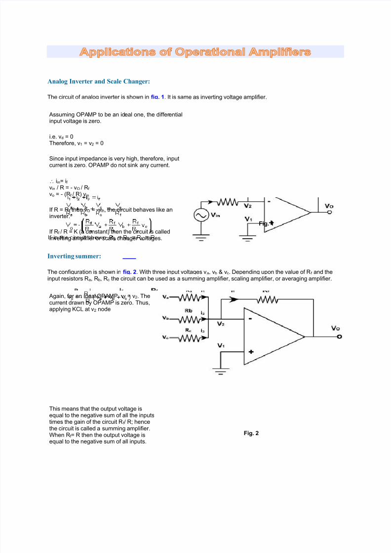
Analog Inverter and Scale Changer:
The circuit of analog inverter is shown in fig. 1. It is same as inverting voltage amplifier.
Assuming OPAMP to be an ideal one, the differentialinput voltage is zero.
i.e. vd = 0Therefore, v1 = v2 = 0
Since input impedance is very high, therefore, inputcurrent is zero. OPAMP do not sink any current.
iin= if vin / R = - vO / Rf
vo = - (Rf / R) vin
If R = Rf then vO = -vin, the circuit behaves like aninverter.
If Rf / R = K (a constant) then the circuit is calledinverting amplifier or scale changer voltages.
Fig. 1
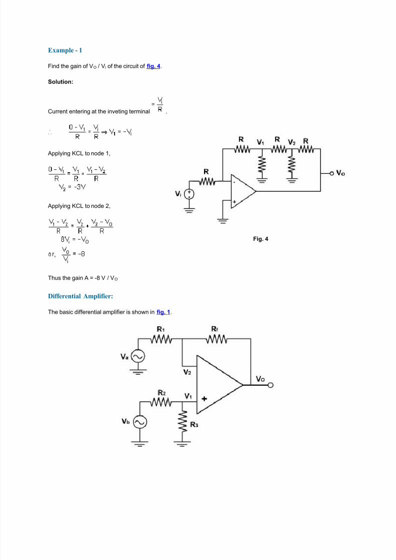
Inverting summer:
The configuration is shown in fig. 2. With three input voltages va, vb & vc. Depending upon the value of R f and theinput resistors Ra, Rb, Rc the circuit can be used as a summing amplifier, scaling amplifier, or averaging amplifier.
Again, for an ideal OPAMP, v1 = v2. Thecurrent drawn by OPAMP is zero. Thus,applying KCL at v2 node
This means that the output voltage isequal to the negative sum of all the inputstimes the gain of the circuit Rf / R; hencethe circuit is called a summing amplifier.When Rf = R then the output voltage isequal to the negative sum of all inputs.
Fig. 2

7/30/2019 Applications of Operational Amplifiers.docx
http://slidepdf.com/reader/full/applications-of-operational-amplifiersdocx 2/11
vo= -(va+ v b+ vc)
If each input voltage is amplified by a different factor in other words weighted differently at the output, the circuit iscalled then scaling amplifier.
The circuit can be used as an averaging circuit, in which the output voltage is equal to the average of all the inputvoltages.
In this case, Ra= Rb= Rc = R and Rf / R = 1 / n where n is the number of inputs. Here R f / R = 1 / 3.
vo = -(va+ vb + vc) / 3
In all these applications input could be either ac or dc.
Noninverting configuration:
If the input voltages are connected to noninverting input through resistors, then the circuit can be used as a summingor averaging amplifier through proper selection of R1, R2, R3 and Rf . as shown in fig. 3.
To find the output voltage expression, v1 is required. Applying superposition theorem, the voltage v1 at thenoninverting terminal is given by
Hence the output voltage is
This shows that the output is equal to the average of all input voltages times the gain of the circuit (1+ R f / R1), hencethe name averaging amplifier.
If (1+Rf / R1) is made equal to 3 then the output voltage becomes sum of all three input voltages.
vo = v a + vb+ vc
Hence, the circuit is called summing amplifier.
7/30/2019 Applications of Operational Amplifiers.docx
http://slidepdf.com/reader/full/applications-of-operational-amplifiersdocx 3/11
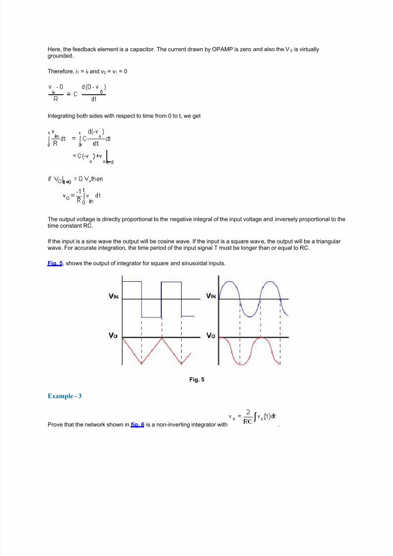
Example - 1
Find the gain of VO / Vi of the circuit of fig. 4.
Solution:
Current entering at the inveting terminal .
Applying KCL to node 1,
Applying KCL to node 2,
Thus the gain A = -8 V / VO
Fig. 4
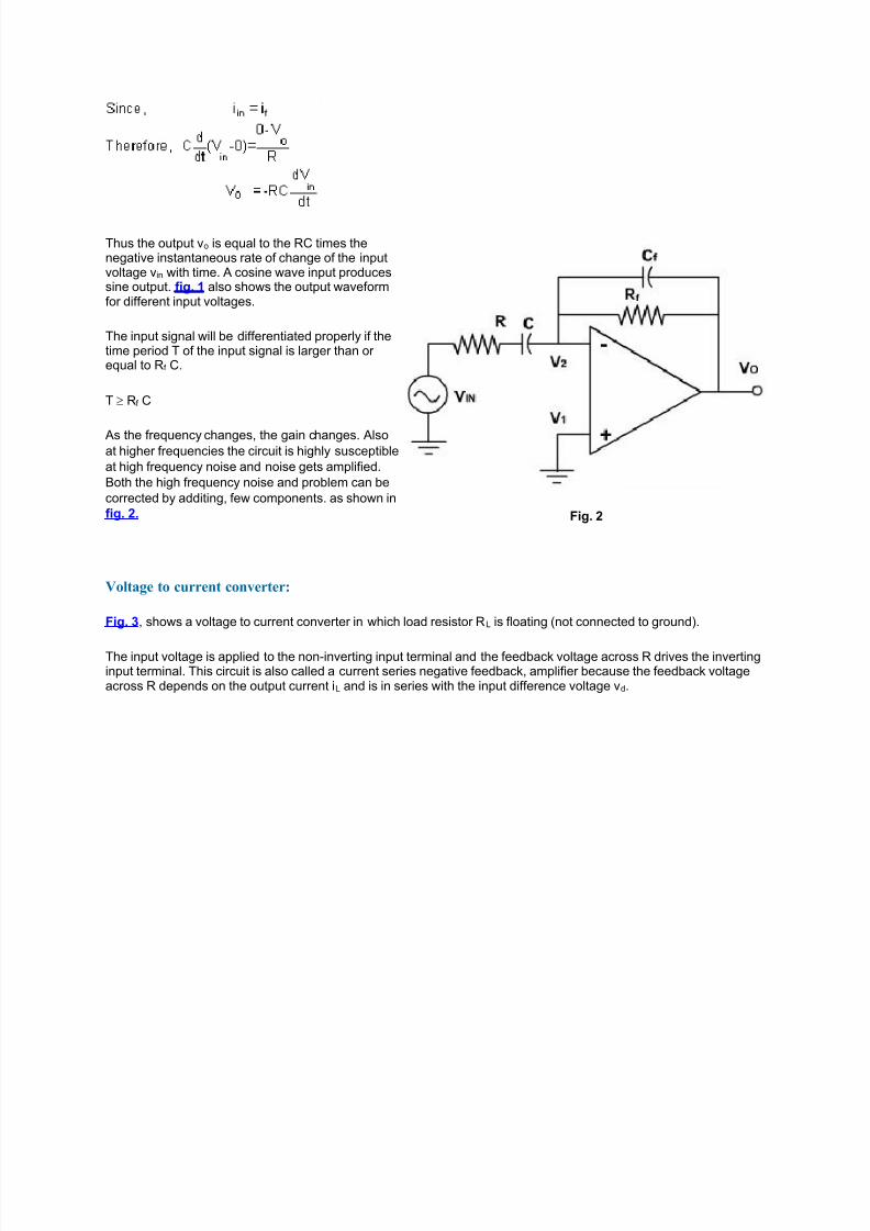
Differential Amplifier:
The basic differential amplifier is shown in fig. 1.

7/30/2019 Applications of Operational Amplifiers.docx
http://slidepdf.com/reader/full/applications-of-operational-amplifiersdocx 4/11
Fig. 1
Since there are two inputs superposition theorem can be used to find the output voltage. When Vb= 0, then the circuitbecomes inverting amplifier, hence the output due to Va only is
Vo(a) = -(Rf / R1) Va
Similarly when, Va = 0, the configuration is a inverting amplifier having a voltage divided network at the noninvertinginput
Integrator:
A circuit in which the output voltage waveform is the integral of the input voltage waveform is called integrator. Fig. 4, shows an integrator circuit using OPAMP.
Fig. 4
7/30/2019 Applications of Operational Amplifiers.docx
http://slidepdf.com/reader/full/applications-of-operational-amplifiersdocx 5/11
Here, the feedback element is a capacitor. The current drawn by OPAMP is zero and also the V2 is virtuallygrounded.
Therefore, i1 = if and v2 = v1 = 0
Integrating both sides with respect to time from 0 to t, we get
The output voltage is directly proportional to the negative integral of the input voltage and inversely proportional to thetime constant RC.
If the input is a sine wave the output will be cosine wave. If the input is a square wave, the output will be a triangular wave. For accurate integration, the time period of the input signal T must be longer than or equal to RC.
Fig. 5, shows the output of integrator for square and sinusoidal inputs.
Fig. 5
Example - 3
Prove that the network shown in fig. 6 is a non-inverting integrator with .

7/30/2019 Applications of Operational Amplifiers.docx
http://slidepdf.com/reader/full/applications-of-operational-amplifiersdocx 6/11
Solution:
The voltage at point A is vO / 2 and it is also the voltage atpoint B because different input voltage is negligible.
vB = VO / 2
Therefore, applying Node current equation at point B,
Differentator:
A circuit in which the output voltage waveform is the differentiation of input voltage is called differentiator.as shown in fig. 1.
Fig. 1
The expression for the output voltage can be obtained from the Kirchoff's current equation written at node v2.
7/30/2019 Applications of Operational Amplifiers.docx
http://slidepdf.com/reader/full/applications-of-operational-amplifiersdocx 7/11
Thus the output vo is equal to the RC times thenegative instantaneous rate of change of the inputvoltage vin with time. A cosine wave input producessine output. fig. 1 also shows the output waveformfor different input voltages.
The input signal will be differentiated properly if thetime period T of the input signal is larger than or equal to Rf C.
T Rf C
As the frequency changes, the gain changes. Alsoat higher frequencies the circuit is highly susceptible
at high frequency noise and noise gets amplified.
Both the high frequency noise and problem can be
corrected by additing, few components. as shown in
fig. 2. Fig. 2
Voltage to current converter:
Fig. 3, shows a voltage to current converter in which load resistor RL is floating (not connected to ground).
The input voltage is applied to the non-inverting input terminal and the feedback voltage across R drives the invertinginput terminal. This circuit is also called a current series negative feedback, amplifier because the feedback voltageacross R depends on the output current iL and is in series with the input difference voltage vd.

7/30/2019 Applications of Operational Amplifiers.docx
http://slidepdf.com/reader/full/applications-of-operational-amplifiersdocx 8/11
Writing the voltage equation for the input loop.
vin = vd + vf
But vd » since A is very large,therefore,
vin = vf vin = R iiniin = v in / R.
and since input current is zero.
iL = iin = vin ./ R
The value of load resistance does not appear inthis equation. Therefore, the output current isindependent of the value of load resistance. Thusthe input voltage is converted into current, thesource must be capable of supplying this loadcurrent. Fig. 3
Grounded Load:
If the load has to be grounded, then the above circuit cannot be used. The modified circuit is shown in fig. 4.
Since the collector and emitter currents are equal to a closeapproximation and the input impedance of OPAMP is veryhigh,the load current also flows through the feedback resistor R.On account of this, there is still current feedback, which meansthat the load current is stabilized.
Since vd= 0 v2 = v1 = vin
iout = (vCC – vin ) / R
Thus the load current becomes nearly equal to iout. There is alimit to the output current that the circuit can supply. The base
current in the transistor equals iout /dc. Since the op-amp has
to supply this base current iout /dc must be less than Iout (max) of the op-amp, typically 10 to 15mA.
There is also a limit on the output voltage, as the load resistanceincreases, the load voltage increases and then the transistor goes into saturation. Since the emitter is at Vin w. r. t. ground, themaximum load voltage is slightly less than V in.
Fig. 4
In this circuit, because of negative feedback VBEis automatically adjusted. For instance, if the load resistance
decreases the load current tries to increase. This means that more voltage is feedback to the inverting input, which
decreases VBE just enough to almost completely nullify the attempted increase in load current. From the output
current expression it is clear that as Vin increases the load current decreases.
Another circuit in which load current increases as Vin increases is shown in fig. 5.

7/30/2019 Applications of Operational Amplifiers.docx
http://slidepdf.com/reader/full/applications-of-operational-amplifiersdocx 9/11
The current through the first transistor is
i = vin / R
This current produces a collector voltage of vC = vCC – i R = vCC – vin
Since this voltage drives the non-invertinginput of the second op-amp. The invertingvoltage is vCC- vin to a close approximation.This implies that the voltage across the finalR is
vCC - (vCC - vin ) = vin
and the output current .
iout = vin / R
As before, this output current must satisfythe condition,that Iout/ dc must be lessthan the Iout(max) of the OPAMP.Furthermore, the load voltage cannot exceedvCC- vin because of transistor saturation,therefore Iout R must be less than vCC-vin.This current source producesunidirectional load current. fig. 6, shows aHowland current source, that can produce abi-directional load current.
Fig. 5
The maximum load current is VCC/ R. In this circuit v in may
Fig. 6

7/30/2019 Applications of Operational Amplifiers.docx
http://slidepdf.com/reader/full/applications-of-operational-amplifiersdocx 10/11
be positive or negative.
Current to voltage converter:
The circuit shown in fig. 1, is a current to voltage converter.
Fig. 1
Due to virtual ground the current through R is zero and the input current flows through Rf . Therefore,
vout =-Rf * iin
The lower limit on current measure with this circuit is set by the bias current of the inverting input.
Example –1:
For the current to current converter shown in fig. 2, prove that
Fig. 2
Solution:
The current through R1 can be obtained from the current divider circuit.

7/30/2019 Applications of Operational Amplifiers.docx
http://slidepdf.com/reader/full/applications-of-operational-amplifiersdocx 11/11
Since, the input impedance of OPAMP is very large, the input current of OPAMP is negligible.
Thus,