applications of xrd mapping to the control of compound semi-conductor processes
TRANSCRIPT

Applications of XRD Mapp,ng t o t h e Control
of ..Compound Sem, conductor
Processes Chris Moore and John Hennessy
The demand for increasing volumes of devices at lower unit costs requires that successful producers of compound semiconductor devices move to full wafer processing and larger wafer sizes. Although processing of full
wafers should, in theory, yield lower unit costs, this is only true if the device yield remains independent of the area processed.
U nfortunately this is seldom the case, and so to obtain equivalent yields a signifi-
cant improvement in material unifor- mity is needed. Without such an increase in material uniformity, using larger substrates leads to a larger amount of scrapped material. Obtain-
ing such an increase in uniformity requires the routine use of a new generation of non-destructive mea- surement tools with the capability to monitor the spatial uniformity of epitaxial layers and substrates.
X-ray topographic and diffracto- metric techniques have been used for
many years to study the quality ot substrates, to measure lattice mis- match and epitaxial layer quality and to monitor epitaxial layer com- position. High speed, high resolution mapping double crystal diffract- ometers extend the use of these techniques to the routine mapping of
+
Incoming X-rays Diffracted X-rays
crystal lattice
Page 14
Fi~dure I.
i / l I I I l I I I , I m C H A R A C T E R I Z A T | O N F E A T U R ~ I
F i r s t C r y s t a l H o l d e r
I , ] ,~X-Ray Detector
Figure 2.
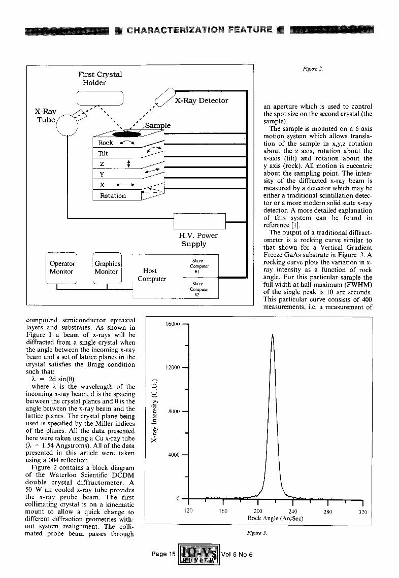
an aperture which is used to control X-Ray ~ - " T u b e ( ~
\ j
Operator Monitor
Rock ~
Tilt • /
z ¢
X ~" ;
Rotation I[_..I- ~
UOrap ics Host
Computer
compound semiconductor epitaxial layers and substrates. As shown in Figure 1 a beam of x-rays will be diffracted from a single crystal when the angle between the incoming x-ray beam and a set of lattice planes in the crystal satisfies the Bragg condition such that:
X = 2d sin(0) where X is the wavelength of the
incoming x-ray beam, d is the spacing between the crystal planes and 0 is the angle between the x-ray beam and the lattice planes. The crystal plane being used is specified by the Miller indices of the planes. All the data presented here were taken using a Cu x-ray tube (X = 1.54 Angstroms). All of the data presented in this article were taken using a 004 reflection.
Figure 2 contains a block diagram of the Waterloo Scientific DCDM double crystal d i f f rac tometer . A 50 W air cooled x-ray tube provides the x-ray probe beam. The first collimating crystal is on a kinematic mount to allow a quick change to different diffraction geometries with- out system realignment. The colli- mated probe beam passes through
~5
e-
l X
16000
12000
8000 m
4000 - -
H.V. P o w e r S u p p l y
Slave Computer
#1
Slave Computer
#2
0 ' I 120 160
the spot size on the second crystal (the sample).
The sample is mounted on a 6 axis motion system which allows transla- tion of the sample in x,y,z rotation about the z axis, rotation about the x-axis (tilt) and rotation about the y axis (rock). All motion is eucentric about the sampling point. The inten- sity of the diffracted x-ray beam is measured by a detector which may be either a traditional scintillation detec- tor or a more modern solid state x-ray detector. A more detailed explanation of this system can be found in reference [1].
The output of a traditional diffract- ometer is a rocking curve similar to that shown for a Vertical Gradient Freeze GaAs substrate in Figure 3. A rocking curve plots the variation in x- ray intensity as a function of rock angle. For this particular sample the full width at half maximum (FWHM) of the single peak is 10 arc seconds. This particular curve consists of 400 measurements, i.e. a measurement of
_5 ' I ' I ;- " - I" ' ' I
200 240 280 320
Rock Angle (ArcSec)
Figure 3.
Page 15 I !ii~! iii~ii i~ill !ii~iii!~:i:~i!'@i'(iii I Vol 6 No 6
. . . . . . . " ; ' ~ " ; . ;> . , ; . . . . . . . . . . . . >. , . . . . . , . . . :i~::;..:.:....., ~ . ; . . . . . . . . ~ . . . . . . . . : . . + . . . . . . . . , . . . , : . . . . . . : , . . . . , . . ; . . : ~ i ~:
8 . 0 ) '
°
21.0"
I I
I I |
I I
[ I 5 m m
F(,cure 4.
x-ray intensity at every 0.25 arc seconds. In the past, diffractometer systems took a few minutes to measure a curve of this type at this resolution, however, newer generation i n s t r u m e n t s (such as the WSI DCDM) can measure a curve of this type in less than one second.
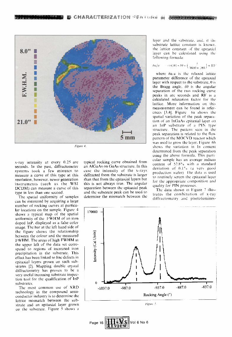
The spatial uniformity of samples can be measured by acquiring a large number of rocking curves at particu- lar locations on the sample. Figure 4 shows a typical map of the spatial unitbrmity of the FWHM of an iron doped InP, displayed as a false color image. The bar at the left hand side of the figure shows the relationship between the colour and the measured FWHM. The areas of high FWHM at the upper left of the data set corre- spond to regions of increased iron precipitation in the substrate. This effect has been linked to line defects in epitaxial layers grown on such sub- strates [2]. Mapping double crystal diffractometry has proven to be a very useful incoming substrate inspec- tion tool for the qualification of InP substrates.
typical rocking curve obtained from an A1GaAs on GaAs structure. In this case the intensity of the x-rays diffracted from the substrate is larger than that from the epitaxial layers but this is not always true. The angular separation between the epitaxial peak and the substrate peak can be used to determine the mismatch between the
170000 -
L"
o
layer and the substrale, and. if tilt substrate lattice constant is known the lattice constant of the cpitaxia] layer can be calct, lated using the t\)llowing l\~rmula:
2~
. , . ( o > • . *
where 6a/a is the relaxed lattice parameter difference of the epitaxial layer with respect to the substrate, 0 is the Bragg angle, 60 is the angular separation of the two rocking curve peaks in arc seconds and RF is a calculated relaxation factor for the lattice. More intk~rmation on this measurement can he found in refer- ences [3,4]. Figure 6a shows the spatial variation of the peak separa- tion of an InGaAs epitaxial layer on an lnP substrate of a PIN type structure. The pattern seen in the peak separation is related to the flow pattern of the MOCVD reactor which was used to grow the layer. Figure 6b shows the variation m In content determined from the peak separation using the above formula. This parti- cular sample has an average indium content of 52.8% ~ith a standard deviation of 0.1".i, {a very good production wafer). l h e data is used to routinely screen the epitaxial layer for the appropriate composition and quality fl)r PIN processes.
The data shown in Figure 7 illus- trates the combina t ion of x-ray diffractometry and photolumines-
The most common use of XRD technology in the compound semi- conductor industry is to determine the lattice mismatch between the sub- stratc and an epitaxial layer grown on the substrate. Figure 5 shows a
0 m ~ . 1
!
-1037.0 -987.0 -937.0
I I
-887.0 -837.0
Rocking Angle C)
Fl~liYC f
Vol 6 N o 6

I I CHARACTERIZATION FEATURE i
5 5 "
.o
ca £a. O
! 55"
[ ]
J I II
m l i 5mm
52.25% •
m
0 tO = !
• - |
II | I! II II I!
53.25% I
Figure 6.
cence mapping. The map in the upper left shows the spatial variation of the wavelength of an InGaAsP epitaxial layer determined by room tempera- ture photoluminescence. The map on the fight shows the variation in lattice mismatch for the same sample as measured by XRD. These two data sets can be combined [5] to produce maps of the compositional variation of the epitaxial layer. The lower map in Figure 7 shows the variation in As
content of this sample. This combina- tion of measurements can be used to routinely monitor quaternary compo- sition, a particularly difficult process control problem.
Material uniformity and consis- tency is a determining factor in obtaining high yield, low unit cost, compound semiconductor devices using full wafer processing of large wafers. Device producers have in- creased yield dramatically as the
1282
! 1340
| I I
|
O
< ,, | I I
II 70 ,
-3~,
8: |
-lfX)'
result of the improved screening of incoming substrates, and better mon- itoring and control of the growth process. Thus, the measurement of the spatial uniformity provided by new generation measurement tools such as double crystal diffractometer mappers is a vital input to the process of improving real wafer yield.
References I. Waterloo Scientific DCDM Ap-
plication Note #1, "An Introduc- tion to Spatially Resolved Double Crystal Diffractometer Measure- ments".
2. Miner, C.J. et al., Proceedings of DRIP V,(1993) I.O.P., in press.
3. Halliwell, M.A.G. et al., J. Cryst. Growth (1983), pp672-678.
4. Waterloo Scientific DCDM Ap- plication Note #2, "Spatially Re- solved Ternary Compos i t ion Mapping Using the Waterloo Scientific DCDM High Speed Mapping Double Crystal Diffract- ometer".
5. Macrander, A.T and Lau, S., J. Electrochem. Soc. Vol 138, No. 4 (1991) pp1147-1153.
Contact: Waterloo Scientific Inc., 419 Phillip Street, Unit 9, Waterloo,
Ontario, Canada N2L 3X2. Tel: [1] (519) 746-6260.
Fax: [1] (519) 746-8270.
Figure 7.
Page 17 I ~ l V 0 1 6 No 6