applied surface science -...
TRANSCRIPT

Nnf
Xa
Xb
c
d
a
ARRAA
KNCAGDN
1
dcsmoihcnwnsbb
t
0h
Applied Surface Science 273 (2013) 816– 823
Contents lists available at SciVerse ScienceDirect
Applied Surface Science
jou rn al h om epa g e: www.elsev ier .com/ locate /apsusc
anoindentation behaviors of amorphous carbon films containinganocrystalline graphite and diamond clusters prepared by radio
requency sputtering
ue Fana,b, Kenji Nosec, Dongfeng Diaoa,d,∗, Toyonobu Yoshidab
Key Laboratory of Education Ministry for Modern Design and Rotor-Bearing System, School of Mechanical Engineering, Xi’an Jiaotong University,i’an 710049, ChinaDepartment of Materials Engineering, Graduate School of Engineering, The University of Tokyo, Tokyo 113-8656, JapanInstitute of Industrial Science, The University of Tokyo, Tokyo 153-8505, JapanNanosurface Science and Engineering Research Institute, Shenzhen University, Shenzhen 518060, China
r t i c l e i n f o
rticle history:eceived 9 September 2012eceived in revised form 29 January 2013ccepted 4 March 2013vailable online 14 March 2013
eywords:
a b s t r a c t
Amorphous carbon (a-C) films were prepared by a radio-frequency sputtering method. Nano structuresin the films were controlled by changing the ion irradiation energy and deposition temperature. It wasfound that nanocrystalline graphite and diamond clusters were embedded in the pure amorphous struc-ture with sizes of approximately 5 nm. a-C films contained nanocrystalline graphite clusters (a-C:NCG)were obtained with the ion energy ranging from 50 to 120 eV and temperature in 300–370 K. a-C filmcontained nanocrystalline diamond clusters (a-C:NCD) was obtained with 120 eV at 570 K. Nanoinden-
anocrystallinearbon filmmorphousraphiteiamondanoindentation
tation behaviors of these carbon films were compared with pure amorphous structured carbon film. Thepercentage of elastic recoveries of a-C:NCD, a-C, and a-C:NCG films were obtained to be 81.9%, 84.3%,and 87.5%, respectively. Pop-in steps with about 3 nm displacement appeared in loading curves for a-C:NCG film, and 10 nm for a-C:NCD film. These results showed that the nanoindentation behaviors ofamorphous carbon film containing cross-linked nanocrystalline graphite clusters is better than that ofdiamond clusters.
. Introduction
Nanocrystalline carbon structures include for example graphite,iamond, fullerene, nanotube, and graphene, and these structuresontribute to their unique characteristics [1]. When nanocrystallinetructured clusters are embedded in the amorphous carbon (a-C)atrix, the excellent characteristics of these clusters enhance the
verall properties of the films. Therefore, the study of a-C filmsncluding nanocrystalline clusters has attracted much attention. Itas been reported that a-C films containing graphite and fullerenelusters exhibited good mechanical properties with higher hard-ess and elastic recovery [2,3] and unique electrical properties [4,5]ithout compromising the tribological properties [6]. When carbonanotubes were embedded into a-C, the field emission current was
ignificantly increased [7]. Lately, graphene sheet embedded car-on films with the �-electronic structure of bilayer graphene haveeen prepared by low-energy electron irradiation, and the films can∗ Corresponding author at: Nanosurface Science and Engineering Research Insti-ute, Shenzhen University, Shenzhen 518060, China. Tel.: +86 755 26902415.
E-mail address: [email protected] (D. Diao).
169-4332/$ – see front matter © 2013 Elsevier B.V. All rights reserved.ttp://dx.doi.org/10.1016/j.apsusc.2013.03.012
© 2013 Elsevier B.V. All rights reserved.
be expected to be applicable in many areas in electronics [8]. Theformation of nanocrystalline structure mainly depends on the filmpreparation technology.
Different methods have been tried to make nanocrystallinestructures in a-C films, for example the filtered cathodic arcdeposition [9], energetic particle bombardment [10], pulsed laserdeposition [11,12], and radio-frequency (RF) sputtering [13,14]. InRF sputtering, ion energy from plasma varies in a wide range, andis easy to control to promote and modify the growth of nanocrys-talline structures in BN films [15]. Schwan et al. observed carbonfilms deposited by RF sputtering and found that small graphiteregions appeared although the film had a high sp3 content [13].Wan and Komvopoulos used a magnetron sputtering system toprepare a-C films and observed clusters of nanocrystalline diamondin these films. They suggested that through the irradiation of argonions, the sp2 bonds in the a-C films were broken and rebound toform diamond clusters [16,17]. Lau et al. studied the ion energy andsubstrate temperature effects on the nanostructure of carbon films
prepared by filtered cathodic arc deposition, and showed that rel-atively high temperature (713 K) and moderate ion energy (95 eV)were proper conditions to form sp2-bonded nanocrystalline clus-ters [18]. However, in the RF sputtering system, less is known about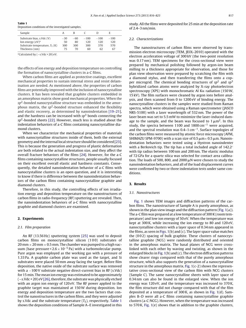
X. Fan et al. / Applied Surface Sci
Table 1Deposition conditions of the investigated samples.
Sample A B C D E
Substrate bias, s.Vdc (V) −30 −60 −100 −100 −100Ion energy (eV)a 50 80 120 120 120Substrate temperature, TS (K) 300 300 300 370 570Thickness (nm) 75 70 60 62 67
a
tt
mificaspaasim
wgTaofioqntid
tctg
2
2
c2uP1sdwf(wgetbs
deposited at a temperature of 300 K, as shown in Fig. 1(d). Sam-
Calculated by (−s.Vdc + 20) eV.
he effects of ion energy and deposition temperature on controllinghe formation of nanocrystalline clusters in a-C films.
When carbon films are applied as protective coatings, excellentechanical properties to sustain internal stress and resist delam-
nation are needed. As mentioned above, the properties of carbonlms are potentially improved with the inclusion of nanocrystallinelusters. It has been revealed that graphite clusters embedded inn amorphous matrix show good mechanical properties. When thep2-bonded nanocrystalline structure was embedded in the amor-hous matrix, the sp2-bonded structure enhanced the flexibilitynd elastic recovery, as determined by nanoindentation [19–21],nd the hardness can be increased with sp3 bonds connecting thep2-bonded sheets [22]. However, much less is studied about thendentation behaviors of a-C films containing nanocrystalline dia-
ond clusters.When we characterize the mechanical properties of materials
ith nanocrystalline structures inside of them, both the externaleometry and the internal local structure should be considered [23].his is because the generation and progress of plastic deformationre both related to the actual indentation size, and they affect theverall fracture behaviors of the films [24]. However, for the a-Clms containing nanocrystalline structures, people usually focusedn their excellent overall elastic and hardness constants. Conse-uently, the detailed nanoindentation behavior of a-C films withanocrystalline clusters is an open question, and it is interestingo know if there is difference between the nanoindentation behav-ors of the carbon films containing nanocrystalline graphite andiamond clusters.
Therefore, in this study, the controlling effects of ion irradia-ion energy and deposition temperature on the nanostructures ofarbon films in radio-frequency (RF) sputtering are revealed. Then,he nanoindentation behaviors of a-C films with nanocrystallineraphite and diamond clusters are examined.
. Experiments
.1. Film preparation
An RF (13.56 Hz) sputtering system [25] was used to depositarbon films on monocrystalline silicon (1 0 0) substrates of0 mm × 20 mm × 0.5 mm. The chamber was pumped to a high vac-um (base pressure < 2.6 × 10⁻⁵ Pa) with a turbomolecular pump.ure argon was employed as the working gas with a pressure of.33 Pa. A graphite carbon plate was used as the target, and Siubstrates were placed 50 mm away facing the target. Before filmeposition, the native oxide of the substrate surface was removedith a −100 V substrate negative direct-current bias in RF (s.Vdc)
or 15 min. The mean ion energy was estimated to be approximately−s.Vdc + 20) eV [26], therefore, the substrate was physically etchedith an argon ion energy of 120 eV. The RF power applied to the
raphite target was maintained at 150 W during deposition. Ionnergy and deposition temperature are the two factors that con-
rol the nanostructures in the carbon films, and they were adjustedy s.Vdc and the substrate temperature (TS), respectively. Table 1hows the deposition conditions of Sample A–E investigated in thisence 273 (2013) 816– 823 817
study. All the films were deposited for 25 min at the deposition rateof 2.4–3 nm/min.
2.2. Characterizations
The nanostructures of carbon films were observed by trans-mission electron microscopy (TEM, JEOL-2010) operated with theelectron acceleration voltage of 300 kV (the two-point resolutionwas 0.17 nm). TEM specimens for the cross-sectional view wereprepared by mechanical polishing followed by argon-ion beammilling to a thickness appropriate for observation, and those forplan view observation were prepared by scratching the film witha diamond stylus, and then transferring the films onto a cop-per microgrid. The chemical bonding structures of sp2 and sp3
hybridized carbon atoms were analyzed by X-ray photoelectronspectroscopy (XPS) with monochromatic Al K� radiation (150 W,15 kV). The film surfaces were cleaned by argon ions before anal-ysis, and then scanned from 0 to 1200 eV of binding energy. Thenanocrystalline clusters in the samples were studied from Ramanspectra, which were obtained using a Raman spectrometer (JASCONRS-5100) with a laser wavelength of 532 nm. The power of thelaser beam was set to 5.5 mW to minimize the laser-induced dam-age to the sample, and the beam was focused to 1 �m2. In thisstudy, the spectra between 1100 and 1800 cm−1 were acquired,and the spectral resolution was 0.4–1 cm−1. Surface topologies ofthe carbon films were measured by atomic force microscopy (AFM,SHIMAZU SPM-9700) with a scan size of 0.5 �m× 0.5 �m. Nanoin-dentation behaviors were tested using a Hystron nanoindenterwith a Berkovich tip. The tip has a total included angle of 142.2◦
with tip radius between 100 nm and 200 nm. The elastic modulusof 72 GPa for a quartz silica was selected for contact area calibra-tion. The loads of 500, 800, and 2000 �N were chosen to study thenanoindentation behaviors, and all of the load displacement curveswere confirmed by two or three indentation tests under same con-ditions.
3. Results
3.1. Nanostructures
Fig. 1 shows TEM images and diffraction patterns of the car-bon films. The nanostructure of Sample A is purely amorphous, asshown in the plan view image and the diffraction pattern (Fig. 1(a)).The a-C film was prepared at a low temperature of 300 K (room tem-perature) and low ion energy of 50 eV. When the temperature waskept at 300 K, while increasing the ion energy to 80 and 120 eV,nanocrystalline clusters with a layer space of 0.34 nm appeared inthe films, as seen in Figs. 1(b) and (c). The layer space value matchesthe (0 0 2) spacing of bulk graphite. These clusters of nanocrys-talline graphite (NCG) were randomly distributed and orientedin the amorphous matrix. The basal planes of NCG were cross-linked with each other by waving and twisting, as shown in theenlarged blocks in Fig. 1(b) and (c). The electron diffraction patternsshow clearer rings compared with that of the purely amorphousstructure, which also supports the generation of a nanocrystallinestructure in the amorphous matrix. Fig. 1(c-2) shows the represen-tative cross-sectional view of the carbon film with NCG clusters(Sample C). The same nanocrystalline sheets with layer space of0.34 nm can also be found in the enlarged view. When the ionenergy was 120 eV, and the temperature was increased to 370 K,the film structure did not change compared with that of the film
ples B–D were all a-C films containing nanocrystalline graphiteclusters (a-C:NCG). However, when the temperature was increasedto 570 K, Fig. 1(e) shows that in addition to the graphite clusters,

818 X. Fan et al. / Applied Surface Science 273 (2013) 816– 823
carbon films observed by TEM.
ss(tastTtc
atsCcoriw
Fig. 1. Nanostructures of
traight planes with a constant distance of about 0.2 nm were pre-ented. This structure is inferred to be nanocrystalline diamondNCD) [4,27]. The cluster size of NCDs was about 5 nm, and the dis-ribution and orientation were random in the amorphous matrixs in the case of NCG. Therefore, from the TEM observations, thetructure of the prepared carbon films was modified from pure a-Co a-C:NCG when the ion energy was increased from 50 to 120 eV.hen, when the ion energy was held at 120 eV and the depositionemperature was increased to 570 K, the structure changed to a-Containing both NCG and NCD clusters (a-C:NCD for short).
Chemical bonds in the films, i.e., sp2 and sp3 hybridized carbontoms, were characterized by XPS. Fig. 2 shows the typical spec-rum of C 1s of the carbon film. In order to quantitatively obtain thep2 and sp3 contents in the investigated carbon films, the original
1s spectrum was deconvoluted into three Gaussian distributionurves. The two curves with peak positions at binding energies
f 284.4 and 285.2 eV represented the sp2 and sp3 hybridizations,espectively. Another weak curve with a peak position at 288.8 eVndicated C O bonds, which meant that a small amount of oxygenas included in the film. The ratio of sp3 to sp2 contents is shown in Fig. 2. C 1s core level spectrum and fitting curves of carbon film (Sample C).

X. Fan et al. / Applied Surface Science 273 (2013) 816– 823 819
Table 2G peak position shift and peak intensity ratio of D peak to G peak.
Carbon films a-C a-C:NCG a-C:NCD
Sample A Sample B Sample C Sample D Sample E
3 2
Thiht1ueSi
tibssrtrs
swwribeut[itset
sp /sp 1.72 1.49
G peak position (cm−1) 1571.6 1569.6
ID/IG 0.368 0.269
able 2. The content of sp3 hybridization was higher than that of sp2
ybridization in all of the investigated samples because the incidenton energy during the deposition provides pressure to form the sp3
ybridization. Sample A with the purely amorphous structure hadhe highest sp3 content. Then, with the increase in ion energy to20 eV and temperature to 370 K, the sp3 content decreased grad-ally. It was also verified from the TEM images which showed thexistence of NCG clusters in Samples B–D. On the other hand, inample E, since the NCD clusters was embedded, the sp3 contentncreased again.
The clustering process of NCG is associated with a change inhe Raman spectrum [28]. Fig. 3 shows the Raman spectra of thenvestigated carbon films. Sample A (a-C) shows a relatively wideand, Samples B,–D (a-C:NCG) exhibit a clearer G peak in the Ramanpectra, and for Sample E (a-C:NCD), the D peak and G peak wereeparated. Since the G peak involves the in-plane bond (chains orings) of sp2 carbon atoms, and the D peak indicates the organiza-ion of sp2 carbon atoms into nanoclusters of sp2-bonded sixfoldings, the change in the Raman spectra was in accordance with thetructural transformations of sp2 clusters in the films [29].
To examine the structural transformation in detail, the Ramanpectra in Fig. 3 were deconvoluted to D and G peaks. The G peakas fitted with a Breit–Wigner–Fano (BWF) function and the D peakith a Lorentzian one [29]. The G peak position and the intensity
atio of the D peak to the G peak (ID/IG) are listed in Table 2. Increas-ng the ion energy from 50 to 120 eV at 300 K, the G peak positionarely changed with the variation of ion irradiation energy, how-ver, it goes to higher values when increasing the temperature. Anpward shift in the G peak position signifies sp2 carbon aggrega-ion into larger clusters with shorter nearest-neighbor distances30]. Sample E also showed an increasing G peak position, whichndicated that sp2 bonds can condense into larger clusters at higheremperature even with increased sp3 content. This is because the
p2 bond is able to diffuse in the a-C matrix and the activationnergy of the diffusion is lower than the conversion energy of sp3o sp2 [31]. The peak density ratio of ID/IG was used to monitor the
Fig. 3. Raman spectra of carbon films.
1.47 1.24 1.611570.8 1578.8 1591.4
0.299 0.477 0.677
evolution of graphitization in the films since ID/IG is normally pro-portional to the clustering of rings. The results of ID/IG showed thesame trend for the G peak position as mentioned above. The higherthe ID/IG, the more clusters of NCG with sp2 bonds are embeddedin the amorphous matrix.
3.2. Surface topographies
Surface topographies of the investigated carbon films and Sisubstrate are shown in Fig. 4. The mean surface roughnesses (Ra)of Samples A (0.052 nm), B (0.050 nm), and C (0.065 nm) were allsmaller than that of Si substrate (0.081 nm). The sputtered ionenergy barely changed the surface roughness at room tempera-ture even if the nanostructure of the films was modified from a-C(Sample A) to a-C:NCG (Samples B and C). When increasing thetemperature from 300 to 370 K, Ra of Sample D (0.62 nm) increasedabout tenfold compared with that of Sample C, as shown in Fig. 4(d),and there were small domes on the surface. Then, upon increasingthe substrate temperature to 570 K, Ra reached 2.74 nm for SampleE and large domes appeared on the film surface dispersedly.
3.3. Nanoindentation behaviors
Nanoindentation behaviors of the carbon films were ana-lyzed from load-displacement curves. Fig. 5 shows the typicalload–displacement curves of three different nanostructured car-bon films and the Si substrate with the maximum indentation loadof 500 �N. All the curves showed consecutive loading and unload-ing processes. On the basis of the load–displacement curves, thehardness (H) and elastic modulus (E) are usually evaluated by theapproach proposed by Oliver and Pharr [32]. The maximum inden-tation depth (hmax), the residual indentation depth (hres), and theelastic recovery (R) are also calculated in relation to H and E. Themaximum indentation depth (hmax) indicates the stiffness of thefilm. Elastic recovery (R) is a factor that affects the ability to pre-vent plastic deformation, and the percentage of R (%R) is calculatedusing hres and hmax, as expressed in the following [33]:
%R = (hmax − hres)hmax
(1)
The values of hmax and %R for Samples A–E with indentationload of 500 �N are listed in Table 3. For comparison, the values ofhardness and elastic modulus calculated by the Power Law Relationwith calibrated contact area function were given in the table. Com-pared with the Si substrate, the a-C film showed a much smallerhmax under the same indentation load. Upon increasing ion energyand deposition temperature, the maximum indentation depths ofa-C:NCG films slightly increased compared with the a-C film, indi-cating that the a-C:NCG films became slightly softer, but were stillharder than the substrate, which can be reflected from the hardnessvalue. When clusters of NCD were embedded in the amorphousmatrix (Sample E), the values of hmax and calculated hardness werenear that of the substrate. That is, the hardness decreased consid-
erably for the a-C:NCD film. As mentioned above, %R is related tothe elastic properties of the material. The Si substrate had the %Rvalue of only 71.4%, and for the carbon film with purely amorphousstructure, %R was approximately 84.3%. When clusters of NCG were
820 X. Fan et al. / Applied Surface Science 273 (2013) 816– 823
(e) fo
e8tr
lp
TM
Fig. 4. Surface topographies of carbon films from (a) to
mbedded, %R was increased to 87.5%. However, %R decreased to1.9% when NCD clusters were embedded. Although the sp3 con-ent increased comparing with a-C:NCG, the hardness and elastic
ecovery of a-C:NCD film were both decreased.Depending on the types of clusters embedded into a-C, theoad–displacement curves showed different characteristics morerominently when the maximum indentation load was increased
able 3aximum indentation depth, hardness, elastic recovery, and elastic modulus for the inve
Sample Si Substrate a-C
Sample A
Maximum indentation depth, hmax (nm) 42.0 35.0
Hardness, H (GPa) 11.01 19.12
% Elastic recovery, %R 71.4% 84.3%
Elastic modulus, E (GPa) 151.08 170.74
r Samples A–E respectively, and that of Si substrate (f).
(i.e., the indentation area was enlarged). The load–displacementcurves of the Si substrate and a-C film exhibited continuous loadingand unloading curves under indentation load of 800 �N, as shown
in Fig. 6. However, for a-C:NCG and a-C:NCD, the loading curvesshowed small but clear discontinuous pop-in steps of about 3 nmdisplacement, as indicated in Fig. 6(a) and the enlarged view inFig. 6(b). Continuously increasing maximum indentation load tostigated samples obtained with nanoindentation load of 500 �N.
a-C:NCG a-C:NCD
Sample B Sample C Sample D Sample E
35.9 36.6 37.1 41.418.04 16.01 15.28 12.2787.5% 86.3% 85.2% 81.9%
170.47 172.12 154.80 148.56

X. Fan et al. / Applied Surface Sci
Fig. 5. Load–displacement curves with maximum indentation load of 500 �N.
F
2lslo
F
ig. 6. Load–displacement curves with maximum indentation load of 800 �N.
000 �N, the load–displacement curves were shown in Fig. 7. Theoading and unloading curves showed continuity for the Si sub-
trate and a-C film. Small discontinuous pop-in steps existed in theoading curve of a-C:NCG film. However, when the indentation loadn a-C:NCD film reached the maximum, a large step of about 10 nmig. 7. Load–displacement curves with maximum indentation load of 2000 �N.
ence 273 (2013) 816– 823 821
starting from the displacement of 90 nm can be observed. Compar-ing the load–displacement curves of a-C, a-C:NCG, and a-C:NCDfilms in Figs. 5–7, the differences of nanoindentation behaviorsamong the three kinds of films get greater and greater upon increas-ing nanoindentation load.
4. Discussion
In the present study, NCG clusters were embedded in the amor-phous matrix, and the basal planes of NCG were cross-linked witheach other by waving and twisting, as shown in Fig. 1(b)–(e). Thebond between the graphitic basal planes is weak van der waals’force. However, in the NCG cluster, the sp2 bond between theneighbor atoms in a basal plane can be broken by ion irradia-tion, producing the unstable and swaying dangling bonds. If twodangling bonds encountered or the dangling bond links with theneighbor atom, a new sp2 or sp3 bond is generated to cross linkthe basal planes. Comparing with the a-C film, the percentage ofelastic recovery increased for the a-C:NCG film, this is presum-ably because the cross links formed between the graphitic basalplanes strengthened the resistance of basal planes to the tensileand compress strains, resulting in a more elastic structure [34].While for the a-C:NCD film, the sp3 content increased forming thenanocrystalline diamond clusters, both the elasticity and the hard-ness decreased. The reason for lower elastic recovery is consideredto be the lower flexibility of sp3 bond in NCD clusters. Althoughthe hardness increases with the increasing of sp3 bond content inamorphous carbon film, we measured a contrary result that thehardness of a-C:NCD film is lower than those of a-C and a-C:NCGfilms, which is supposed that when the grain size of NCD clustersis small, and the grain boundary sliding becomes more active inmicro-deformation process, referred to as the “reverse Hall–Petcheffect” [35]. Hence, the embedded NCD clusters weakened the over-all mechanical property analyzed in the nanoindentation.
When the indentation load increased, the loading curves ofa-C:NCG and a-C:NCD films show pop-in steps, as shown inFigs. 6 and 7. It should be mentioned that although the films showeda much rougher surface than a-C film, the domes were distributeddispersedly, height scan was performed to move the asperitiesaway from the indentation center before the test, and a flat areawas chosen to avoid the effects of surface roughness on the appear-ance of pop-ins during indentation. Moreover, no pop-out appearedneither in the unloading curves of carbon films nor in that of Si sub-strate, which means that no press induced phase transformationhappened in the substrate [36]. Thereafter, pop-in steps occurredin the film independent of the surface roughness and the steps arenot induced by the silicon substrate.
Then, the effect of carbon films on the appearance of pop-insteps is considered. It has been revealed that these steps are alsorelated to the dislocations in the film structure [24] or brittle frac-ture through the film thickness [37]. For the pop-ins with about3 nm displacements, the steps are much smaller than the film thick-ness and the steps only existed in the films with nanocrystallineclusters, it is inferred that the pop-in steps are caused by the dis-locations in the structure of films containing NCG or NCD clusters.For the a-C:NCG and a-C:NCD films, nanocrystalline clusters embedin the amorphous matrix forming the local discontinuities in thestructure, and dislocations exist in the film. During indentation, thefirst appearance of pop-in indicates the onset of dislocation plas-ticity when the maximum shear stress under the indenter is highenough [38], and the critical shear stress for heterogeneous is much
smaller than that of homogeneous [39]. Therefore, upon increas-ing the indentation load, pop-ins appeared in the a-C:NCG anda-C:NCD films other than in the a-C film. Meanwhile, the motionof preexisting dislocations, the size, the density and the strength of
8 ce Sci
d[ptfipttbostCdotfin
5
iaeNtabaCpapnncta
A
KetbNC
R
[
[
[
[
[
[
[
[
[
[
[
[
[
[
[
[
[
[
[
[
[
[
[
[
[
22 X. Fan et al. / Applied Surfa
efects (NCG and NCD clusters) also affect the appearance of pop-in24], these complicated factors result in the stochastic behavior ofop-ins with different indentation loads. As the maximum inden-ation load became greater, a large step appeared for the a-C:NCDlm at the maximum indentation load, the sudden increase in dis-lacement happened at an indentation depth deeper than the filmhickness, which means that after the indenter has penetrated tohe substrate, a through thickness crack can be generated for therittle diamond clusters embedded film, resulting in a separationf partial film under or around the indenter from the film. Then, thetresses which partly support the indenter are suddenly removedo form a large discontinuity. The nanoindentation behaviors of a-:NCG and a-C:NCD films were obtained with small load, and it isifficult to find the small impressions by the small observation areaf AFM or SEM. In order to clarify the mechanism of nanoindenta-ion behavior, the deformation processes of a-C:NCG and a-C:NCDlms during nanoindentation will be observed by in situ TEM in theear future.
. Conclusions
Nanostructures in a-C films were controlled by RF sputter-ng. NCG clusters occurred in the purely amorphous structurend the size and content increased with the increasing of ionnergy to 120 eV and deposition temperature to 370 K. BothCG and NCD clusters formed in the amorphous matrix when
he film was deposited with ion energy of 120 eV and temper-ture of 570 K. The a-C:NCG films with cross-linked graphiticasal planes showed higher elastic recovery than that of pure-C film, while, a-C:NCD films showed a lower elastic recovery.omparing with the continuous loading curve of pure a-C film,op-in steps occurred both in the loading curves of a-C:NCGnd a-C:NCD films, and the a-C:NCD film showed a much largerop-in step than the a-C:NCG film. The results showed that theanoindentation behaviors of amorphous carbon films containinganocrystalline graphite clusters are better than that of diamondlusters. This study indicates that the dependence of nanoinden-ation behavior on cluster characteristics should be considered inpplication.
cknowledgements
The main author is very grateful to Associate Professor Makotoambara of the University of Tokyo for his help in arrangingxperimental equipment. This work is partially supported byhe National Nature Science Foundation of China (Grant Num-er: 90923027), the China Postdoctoral Science Foundation (Grantumber: 2012M521755), and the PhD Mobility Program of thehina Scholarship Council.
eferences
[1] P.K. Chu, L.H. Li, Characterization of amorphous and nanocrys-talline carbon films, Materials Chemistry and Physics 96 (2006)253–277.
[2] R.G. Lacerda, P. Hammer, C.M. Lepienski, F. Alvarez, F.C. Marques, Hardgraphitic-like amorphous carbon films with high stress and local micro-scopic density, Journal of Vacuum Science and Technology A 19 (2001)971–975.
[3] Q. Wang, C.B. Wang, Z. Wang, J.Y. Zhang, D.Y. He, Fullerene nanostructure-induced excellent mechanical properties in hydrogenated amorphous carbon,Applied Physics Letters 91 (2007) 141902.
[4] V.L. Kuznetsov, Y.V. Butenko, A.L. Chuvilin, A.I. Romanenko, A.V. Okotrub, Elec-trical resistivity of graphitized ultra-disperse diamond and onion-like carbon,Chemical Physics Letters 336 (2001) 397–404.
[5] S. Hirono, S. Umemura, M. Tomita, R. Kaneko, Super-hard conduc-tive carbon nano-crystallite films, Applied Physics Letters 80 (2002)425–427.
[6] Y.J. Wang, H.X. Li, L. Ji, F. Zhao, Q.H. Kong, Y.X. Wang, X.H. Liu, W.L.Quan, H.D. Zhou, J.M. Chen, Microstructure, mechanical and tribological
[
ence 273 (2013) 816– 823
properties of graphite-like amorphous carbon films prepared by unbal-anced magnetron sputtering, Surface and Coatings Technology 205 (2011)3058–3065.
[7] P. Hojati-Talemi, G.P. Simon, Enhancement of field emission of carbon nano-tubes using a simple microwave plasma method, Carbon 49 (2011) 484–486.
[8] C. Wang, D.F. Diao, X. Fan, C. Chen, Graphene sheets embedded carbon filmprepared by electron irradiation in ECR plasma, Applied Physics Letters 100(2012) 231909.
[9] D.W.M. Lau, D.G. McCulloch, M.B. Taylor, J.G. Partridge, D.R. McKenzie, N.A.Marks, E.H.T. Teo, B.K. Tay, Abrupt stress induced transformation in amorphouscarbon films with a highly conductive transition phase, Physical Review Letters100 (2008) 176101.
10] E.H.T. Teo, J. Kulik, Y. Kauffmann, R. Kalish, Y. Lifshitz, Nanostructured car-bon films with oriented graphitic planes, Applied Physics Letters 98 (2011)123104.
11] E. Cappelli, S. Orlando, G. Mattei, P. Zoffoli, Ascarelli SEM and Raman investiga-tion of RF plasma assisted pulsed laser deposited carbon films, Applied SurfaceScience 197–198 (2002) 452–457.
12] J. Eskusson, R. Jaaniso, E. Lust, Diamond-like phase formation in an amorphouscarbon films prepared by periodic pulsed laser deposition and laser irradiationmethod, Applied Surface Science 255 (2009) 7104–7108.
13] J. Schwan, S. Ulrich, T. Theel, H. Roth, H. Ehrhardt, P. Becker, S.R.P. Silva, Stress-induced formation of high-density amorphous carbon thin films, Journal ofApplied Physics 82 (1997) 6024–6030.
14] S. Logothetidis, M. Gioti, P. Patsalas, C. Charitidis, Insights on the deposi-tion mechanism of sputtered amorphous carbon films, Carbon 37 (1999)765–769.
15] K. Nose, K. Tachibana, T. Yoshida, Rectification properties of layered boronnitride films on silicon, Applied Physics Letters 83 (2003) 943–945.
16] D. Wan, K. Komvopoulos, Transmission electron microscopy and electronenergy loss spectroscopy analysis of ultrathin amorphous carbon films, Journalof Materials Research 19 (2004) 2131–2136.
17] D. Wan, K. Komvopoulos, Formation of diamondlike nanocrystallites in amor-phous carbon films synthesized by radio-frequency sputtering, Journal ofMaterials Research 23 (2008) 700–703.
18] D.W.M. Lau, A. Moafi, M.B. Taylor, J.G. Partridge, D.G. McCulloch, R.C. Powles,D.R. McKenzie, The structural phases of non-crystalline carbon prepared byphysical vapor deposition, Carbon 47 (2009) 3263–3270.
19] C. Iwamoto, H.S. Yang, S. Watanabe, T. Yoshida, Dynamic and atomistic defor-mation of sp2-bonded boron nitride nanoarrays, Applied Physics Letters 83(2003) 4402–4404.
20] J. Neidhardt, Z. Czigany, L. Hultman, Superelastic fullerene-like carbon nitridecoatings synthesized by reactive unbalanced magnetron sputtering, SurfaceEngineering 19 (2003) 299–303.
21] Z. Wang, J.Y. Zhang, Deposition of hard elastic hydrogenated fullerenelike car-bon films, Journal of Applied Physics 109 (2011) 103303.
22] W. Guo, C.Z. Zhu, T.X. Yu, C.H. Woo, B. Zhang, Y.T. Dai, Formation of sp3 bondingin nanoindented carbon nanotubes and graphite, Physical Review Letters 93(2004) 245502.
23] D.U. Michael, M.D. Dennis, N.F. Jeffrey, D.N. William, Sample dimensions influ-ence strength and crystal plasticity, Science 305 (2004) 986–989.
24] J.R. Morris, H. Bei, G.M. Pharr, E.P. George, Size effects and stochastic behaviorof nanoindentation pop in, Physical Review Letters 106 (2011) 165502.
25] O. Tsuda, Y. Yamada, T. Fujii, T. Yoshida, Preparation of cubic boron nitride filmsby radio frequency bias sputtering, Journal of Vacuum Science and TechnologyA 13 (1995) 2843–2847.
26] O. Tsuda, Y. Tatebayashi, Y. Takamura-Yamada, T. Yoshida, Mass and energymeasurements of the species responsible for cBN growth in rf bias sputterconditions, Journal of Vacuum Science and Technology A 15 (1997) 2859–2863.
27] H. Sjostrom, L. Hultman, J.E. Sundgren, S.V. Hainsworth, T.F. Page, G.S.A.M.Theunissen, Structural and mechanical properties of carbon nitride CNx
(0.2 ≤ x ≤ 0.35) films, Journal of Vacuum Science and Technology A 14 (1996)56–62.
28] M. Chhowalla, A.C. Ferrari, J. Robertson, G.A.J. Amaratunga, Evolution of sp2
bonding with deposition temperature in tetrahedral amorphous carbon studiedby Raman spectroscopy, Applied Physics Letters 76 (2000) 1419–1421.
29] A.C. Ferrari, J. Robertson, Resonant Raman spectroscopy of disordered, amor-phous, a diamondlike carbon, Physical Review B 64 (2001) 075414.
30] J.O. Orwa, I. Andrienko, J.L. Peng, S. Prawer, Y.B. Zhang, S.P. Lau, Thermallyinduced sp2 clustering in tetrahedral amorphous carbon (ta-C) films, Journalof Applied Physics 96 (2004) 6286–6297.
31] A.C. Ferrari, S.E. Rodil, J. Robertson, W.I. Milne, Is stress necessary to stabilisesp3 bonding in diamond-like carbon? Diamond and Related Materials 11 (2002)994–999.
32] W.C. Oliver, G.M. Pharr, An improved technique for determining hardness andelastic modulus using load and displacement sensing indentation experiments,Journal of Materials Research 7 (1992) 1564–1583.
33] T.F. Page, S.V. Hainsworth, Using nanoindentation techniques for the charac-terization of coated systems: a critique, Surface and Coatings Technology 61(1993) 201–208.
34] M.K. Zalalutdinov, J.T. Robinson, C.E. Junkermeier, J.C. Culbertson, T.L. Reinecke,
R. Stine, P.E. Sheehan, B.H. Houston, E.S. Snow, Engineering graphene mechan-ical systems, Nano Letters 12 (2012) 4212–4218.35] I.N. Remediakis, G. Kopidakis, P.C. Kelires, Reverse Hall–Petch effect in ultrananocrystalline diamond, in: Proceedings of the IUTAM Symposium on Mod-elling Nanomaterials and Nanosystems, Aalborg, Denmark, May 19–22, 2008.

ce Sci
[
[
X. Fan et al. / Applied Surfa
36] T. Juliano, V. Domnich, Y. Gogotsi, Examining pressure-induced phase trans-formations in silicon by spherical indentation and Raman spectroscopy: astatistical study, Journal of Materials Research 19 (2004) 3099–3108.
37] X.D. Li, D.F. Diao, B. Bhushan, Fracture mechanisms of thin amorphous carbonfilms in nanoindentation, Acta Materialia 45 (1997) 4453–4461.
[
[
ence 273 (2013) 816– 823 823
38] S. Shim, H. Bei, E.P. George, G.M. Pharr, A different type of indentation sizeeffect, Scripta Materialia 59 (2008) 1095–1098.
39] H. Bei, Y.F. Gao, S. Shim, E.P. George, G.M. Pharr, Strength differences aris-ing from homogeneous versus heterogeneous dislocation nucleation, PhysicalReview B 77 (2008), 060103.