approaches and designs of dynamic voltage and frequency...
TRANSCRIPT
Approaches and Designs of Dynamic Voltage and FrequencyScaling
By
WAYNE HUNG CHENGB.S.E.E. (University of California San Diego) June 2005
THESIS
Submitted in partial satisfaction of the requirements for the degree of
MASTERS OF SCIENCE
in
Electrical and Computer Engineering
in the
OFFICE OF GRADUATE STUDIES
of the
UNIVERSITY OF CALIFORNIA
DAVIS
Approved:
Chair, Dr. Bevan Baas
Member, Dr. Rajeevan Amirtharajah
Member, Dr. Soheil Ghiasi
Committee in charge2008
– i –

c© Copyright by Wayne Hung Cheng 2008All Rights Reserved
Abstract
Techniques for reducing both dynamic and leakage power of a single-chip
multiprocessor while minimizing area and performance overhead are examined within
this thesis. Variations in the workload across processors allow for reducing the supply
voltage and clock frequency to save power. The design decisions are arrived by thor-
ough investigations into the tradeoffs between various ideas, both from the author and
from other experiments. A dynamic voltage and frequency scaling (DVFS) circuit is
designed as a wrapper to the AsAP (Asynchronous Array of Simple Processors) pro-
cessor core. Dynamic power reduction is accomplished through voltage scaling across
two voltage supplies with PMOS power gates. Shutting the power gates off for unused
processors provides additional leakage power savings. Adding additional power gates
in parallel and decoupling capacitors help to combat the performance overhead of
using power gates. A complex supply switching logic design ensures proper operation
through processor stall signals, and guards against shorting the supplies and exces-
sive power grid noise. Workload is determined by the utilization of the processor’s
input FIFOs, and analysis is performed by a configurable FIR/IIR filter. The clock
frequency and supply voltage are scaled dynamically based on the workload. The
highly configurable interface of the dynamic voltage and frequency scaling circuit al-
lows for enough flexibility to handle the various applications that an AsAP processor
can support. Results show significant reductions in dynamic power and energy with
relatively small area and performance overhead. The design is implemented on an
AsAP architecture with an 11.5% area overhead. On a 9 processor JPEG application
with two voltage supplies of 1.3 V and 0.8 V, running with DVFS resulted in an av-
erage of almost half of original energy consumption (52%), with an 8% performance
overhead. The average relative energy delay product was 56%.
– ii –
Acknowledgments
I would like to thank Prof. Bevan Baas for all his invaluable advice on engineering
and topics of life. By taking me under his wings and setting me up with one of the most
prestigious research groups at UC Davis, for that I am deeply in gratitude. I thank him
for trusting me with such an enormous responsibility of designing a novel approach to
dynamic voltage and frequency scaling, and helping me hammer out bugs along the way.
His mentoring and support has not only helped me become a better engineer, but a better
person as well.
I would like to thank the members of my thesis committee. Thanks for Prof.
Amirtharajah for inspiring me to take on topics of analog and low power designs. Thanks
for Prof. Ghiasi for his close work with our group and his genuine interest in my research
topic.
I would like to thank my family, who instilled the values that made me into this
person I am today. I thank my Dad for passing on his tireless work habits, and I thank
my Mom for teaching me compassion towards others. I also thank my brother who always
watched out for me.
I would like to thank my fellow colleagues at VCL. In no particular order: Zhiyi
Yu, Tinoosh Mohsenin, Dean Truong, Zhibin Xiao, Paul Mejia, Eric Work, and Toney
Jacobson. Thank you for the inspiration in my research work and the good times we had.
To the crew that stuck around for every tapeout, I appreciate and admire your sacrifices to
realize the ultimate chip.
Finally, I would like to thank Discovery Christian Church in Davis. I would like to
thank my pastor John Richert, and my fellow disciples Joshua Go and Daniel Meyerpeter.
This work was supported in part by Intel Corporation, UC MICRO, the National
Science Foundation under Grant No. 0430090 and CAREER Award 0546907, SRC, Intel-
lasys Corporation, ST Microelectronics, SEM, MOSIS, Artisan, and a University of Cali-
fornia, Davis, Faculty Research Grant.
– iii –

Contents
Abstract ii
Acknowledgments iii
List of Figures v
List of Tables vii
1 Introduction 11.1 Target System . . . . . . . . . . . . . . . . . . . . . . . . . . . . . . . . . . 31.2 Design Goals . . . . . . . . . . . . . . . . . . . . . . . . . . . . . . . . . . . 3
2 Voltage Scaling 62.1 Voltage Scaling Methods . . . . . . . . . . . . . . . . . . . . . . . . . . . . . 62.2 Power Distribution . . . . . . . . . . . . . . . . . . . . . . . . . . . . . . . . 82.3 Power Gate Design . . . . . . . . . . . . . . . . . . . . . . . . . . . . . . . . 92.4 Performance Overhead . . . . . . . . . . . . . . . . . . . . . . . . . . . . . . 112.5 Supply Switching Methods . . . . . . . . . . . . . . . . . . . . . . . . . . . . 122.6 Communication Across Multiple Voltage Domains . . . . . . . . . . . . . . 152.7 Fail-safe Methods . . . . . . . . . . . . . . . . . . . . . . . . . . . . . . . . . 18
3 Dynamic Voltage and Frequency Scaling Controller 193.1 Workload Analysis . . . . . . . . . . . . . . . . . . . . . . . . . . . . . . . . 193.2 Frequency Scaling . . . . . . . . . . . . . . . . . . . . . . . . . . . . . . . . 243.3 Voltage Scaling . . . . . . . . . . . . . . . . . . . . . . . . . . . . . . . . . . 24
4 Hardware Implementation 264.1 Voltage Scaling Details . . . . . . . . . . . . . . . . . . . . . . . . . . . . . . 264.2 Dynamic Voltage and Frequency Scaling Controller Details . . . . . . . . . 324.3 Final Chip Implementation Details and Results . . . . . . . . . . . . . . . . 45
5 Results 49
6 Conclusion 62
Bibliography 63
– iv –
List of Figures
1.1 Dynamic voltage and frequency scaling for a multiprocessor architecture . . 31.2 Normalized power and delay behavior with voltage scaling . . . . . . . . . . 4
2.1 Dynamic voltage and frequency scaling with two voltage supplies . . . . . . 82.2 Power gate placement and composition . . . . . . . . . . . . . . . . . . . . . 102.3 Circuit to estimate performance loss associated with the power gates . . . . 132.4 Comparison of performance loss vs ratio of area devoted to power gate width
and area devoted to decoupling capacitors . . . . . . . . . . . . . . . . . . . 142.5 Supply switch modules . . . . . . . . . . . . . . . . . . . . . . . . . . . . . . 162.6 Supply switch timing diagram of the supply switch modules . . . . . . . . . 172.7 Example variable buffer chain behaviors . . . . . . . . . . . . . . . . . . . . 17
3.1 Main DVFS circuit with DVFS controller . . . . . . . . . . . . . . . . . . . 203.2 An example configuration of a 5 point adjustable FIR/IIR filter . . . . . . . 223.3 Frequency response of the DVFS filter . . . . . . . . . . . . . . . . . . . . . 233.4 An example of the range of operable frequencies with its corresponding volt-
age supplies . . . . . . . . . . . . . . . . . . . . . . . . . . . . . . . . . . . . 25
4.1 Supply Switch Logic Module in detail . . . . . . . . . . . . . . . . . . . . . 274.2 Supply Switch Timing in detail . . . . . . . . . . . . . . . . . . . . . . . . . 284.3 Variable Buffer Chain in detail . . . . . . . . . . . . . . . . . . . . . . . . . 294.4 Variable Delay Mechanism in detail . . . . . . . . . . . . . . . . . . . . . . . 304.5 Complete DVFS logic block diagram . . . . . . . . . . . . . . . . . . . . . . 354.6 5 point FIR/IIR filter . . . . . . . . . . . . . . . . . . . . . . . . . . . . . . 364.7 Stall counter . . . . . . . . . . . . . . . . . . . . . . . . . . . . . . . . . . . 374.8 Frequency Converter . . . . . . . . . . . . . . . . . . . . . . . . . . . . . . . 384.9 Voltage Switch Counter . . . . . . . . . . . . . . . . . . . . . . . . . . . . . 394.10 Simplified oscillator diagram . . . . . . . . . . . . . . . . . . . . . . . . . . . 394.11 Frequency Interpreter . . . . . . . . . . . . . . . . . . . . . . . . . . . . . . 404.12 Voltage chooser . . . . . . . . . . . . . . . . . . . . . . . . . . . . . . . . . . 414.13 DVFS circuit implemented on an AsAP processor core . . . . . . . . . . . . 464.14 Power gate implementation . . . . . . . . . . . . . . . . . . . . . . . . . . . 474.15 Power gate transistor width vs. processor performance loss . . . . . . . . . 484.16 DVFS area composition . . . . . . . . . . . . . . . . . . . . . . . . . . . . . 48
5.1 Demonstration of DVFS functionality . . . . . . . . . . . . . . . . . . . . . 505.2 Relative power for DVFS on a 9 processor JPEG application . . . . . . . . 52
– v –
5.3 Relative energy delay product with DVFS compared to a non-DVFS designon a 9 processor JPEG application . . . . . . . . . . . . . . . . . . . . . . . 53
5.4 Relative power for DVFS on various applications . . . . . . . . . . . . . . . 545.5 Relative energy delay product with DVFS compared to a non-DVFS design
for various applications . . . . . . . . . . . . . . . . . . . . . . . . . . . . . . 555.6 Relative energy delay product while varying voltages on V ddLow . . . . . . 565.7 The voltage of V ddLow with V ddHigh of 1.3 V with the performance over-
head constrained at 10% . . . . . . . . . . . . . . . . . . . . . . . . . . . . . 575.8 The voltage of V ddLow with V ddHigh of 1.3 V with the performance over-
head constrained at 20% . . . . . . . . . . . . . . . . . . . . . . . . . . . . . 575.9 Demonstration of the variable buffer chain . . . . . . . . . . . . . . . . . . . 585.10 Power grid noise and switching delay of the variable buffer chain . . . . . . 595.11 Circuit used to test the tradeoff between power grid noise and switching delay 60
– vi –
List of Tables
1.1 The Future Trend in Silicon Technology [1] . . . . . . . . . . . . . . . . . . 5
4.1 Configuration for the supply switch modules for AsAP 2 . . . . . . . . . . . 314.2 9 Stage Oscillator Configurations and Results . . . . . . . . . . . . . . . . . 424.3 Configuration for dynamic voltage and frequency scaling circuit . . . . . . . 434.4 Wire Aliases used in the detailed diagrams . . . . . . . . . . . . . . . . . . . 444.5 Configuration for frequency choosing mux (not pictured) . . . . . . . . . . . 444.6 Software configuration of voltage and frequency . . . . . . . . . . . . . . . . 44
5.1 Comparison with previous work . . . . . . . . . . . . . . . . . . . . . . . . . 61
– vii –
1
Chapter 1
Introduction
Advances in portable applications over the last decade has led to demands for
longer battery life. Improvements in battery life have been slow in comparison to the
development of features on portable applications. This dilemma has lead to an increased
focus in power consumption reduction in the semiconductor industry.
Reducing dynamic and leakage power is a problem that has been thoroughly in-
vestigated. Methods of power reduction include operating on multiple supply voltages, and
using sleep transistors to shut off power during idle periods of execution [2] [3]. Lower-
ing the supply voltage leads to a quadratic reduction in dynamic power as evident by the
power-voltage relationship
Pdyn = αCV 2ddf (1.1)
where α is the switching probability, C is the total transistor gate capacitance of the entire
module, V dd is the supply voltage, and f is the clock frequency. However, a reduction in
voltage results in increased delay (td) for the circuit [4]
td ∝V dd
V dd− Vt(1.2)
where Vt is the threshold voltage. To lower the supply voltage without impacting the
overall performance of a system, the system can run at a higher voltage during periods of
high workloads and run at a lower voltage during periods of low workloads. Voltage scaling
schemes that operate during runtime are known as dynamic voltage scaling (as opposed
2 CHAPTER 1. INTRODUCTION
to static voltage scaling schemes such as clustered voltage scaling [5] [6]). The system
frequency needs to scale along with the voltage to ensure that the operating frequency does
not exceed the limits of its critical path.
Leakage power can be reduced by voltage scaling and sleep transistors. Both sub-
threshold leakage (Psub leakage ∝ 1 − eV dd) and gate leakage (Pgate leakage ∝ V dd2/eV dd)
are a function of the supply voltage. DVFS becomes increasingly important as leakage
power continues to become a dominant contribution to power consumption for future sil-
icon technologies [1]. Sleep transistors specifically target leakage power. By cutting off
power from the system during idle periods, sleep transistors can dramatically reduce leak-
age current [7] [8] [9].
Without altering the supply voltage, power can be reduced through frequency
scaling, but the total energy consumption per operation remains the same (assuming the
same number of gate switching occurs). Voltage scaling contributes directly to energy
reduction, where the dynamic energy consumption of a gate is a direct function of the
supply voltage: Energy = CLV dd2, with CL as the load capacitance of a gate.
Dynamic voltage and frequency scaling (DVFS) can be applied to different levels of
granularity. Approaches to DVFS include scaling large modules, to scaling individual logic
blocks on the critical path [10]. The smaller the granularity, the more complex the design
and the larger the overhead. The trend towards multi-processor architectures makes scaling
on individual processors an attractive approach. Many applications tend to map well on
parallel processing architectures, especially digital signal processing applications [11].
In addition to reducing power consumption, DVFS can provide benefits to process
variations and thermal control. It has been shown that process variations will play more
significant roles as transistor scaling continues [12], and the impact of variations can be
mitigated through new design methodologies [13] [14]. A method to combat variations is
by employing higher voltages on the slower gates on the chip to increase performance, and
using lower voltages on the faster gates to decrease leakage. The chip can be configured
in so that most of the gates will exhibit the same leakage and delay characteristics [10].
Similarly, the chip can be configured to place a limit on the maximum chip temperature at
the expense of performance [15].
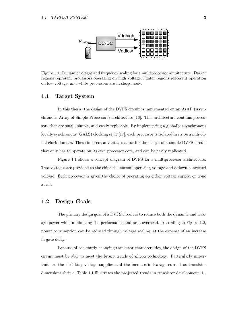
1.1. TARGET SYSTEM 3
DC-DCVddhigh
Vddlow
Vbattery
Figure 1.1: Dynamic voltage and frequency scaling for a multiprocessor architecture. Darkerregions represent processors operating on high voltage, lighter regions represent operationon low voltage, and white processors are in sleep mode.
1.1 Target System
In this thesis, the design of the DVFS circuit is implemented on an AsAP (Asyn-
chronous Array of Simple Processors) architecture [16]. This architecture contains proces-
sors that are small, simple, and easily replicable. By implementing a globally asynchronous
locally synchronous (GALS) clocking style [17], each processor is isolated in its own individ-
ual clock domain. These inherent advantages allow for the design of a simple DVFS circuit
that only has to operate on its own processor core, and can be easily replicated.
Figure 1.1 shows a concept diagram of DVFS for a multiprocessor architecture.
Two voltages are provided to the chip: the normal operating voltage and a down-converted
voltage. Each processor is given the choice of operating on either voltage supply, or none
at all.
1.2 Design Goals
The primary design goal of a DVFS circuit is to reduce both the dynamic and leak-
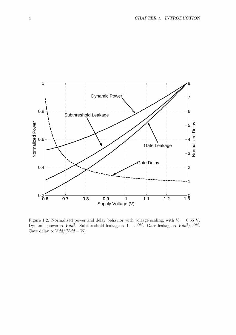
age power while minimizing the performance and area overhead. According to Figure 1.2,
power consumption can be reduced through voltage scaling, at the expense of an increase
in gate delay.
Because of constantly changing transistor characteristics, the design of the DVFS
circuit must be able to meet the future trends of silicon technology. Particularly impor-
tant are the shrinking voltage supplies and the increase in leakage current as transistor
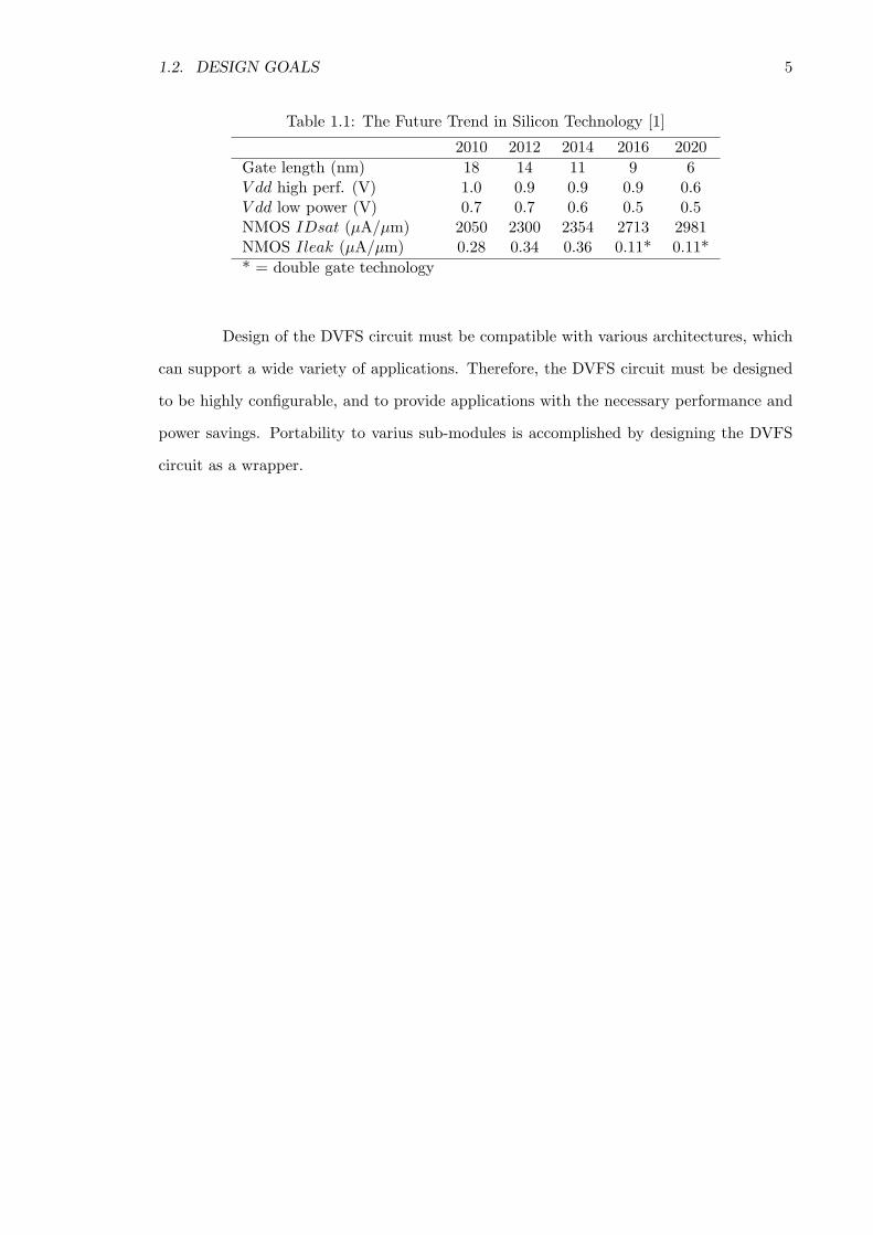
dimensions shrink. Table 1.1 illustrates the projected trends in transistor development [1].
4 CHAPTER 1. INTRODUCTION
0.6 0.7 0.8 0.9 1 1.1 1.2 1.30.2
0.4
0.6
0.8
1
Nor
mal
ized
Pow
er
Supply Voltage (V)0.6 0.7 0.8 0.9 1 1.1 1.2 1.3
0
1
2
3
4
5
6
7
8
Nor
mal
ized
Del
ay
Dynamic Power
Subthreshold Leakage
Gate Leakage
Gate Delay
Figure 1.2: Normalized power and delay behavior with voltage scaling, with Vt = 0.55 V.Dynamic power ∝ V dd2. Subthreshold leakage ∝ 1 − eV dd. Gate leakage ∝ V dd2/eV dd.Gate delay ∝ V dd/(V dd− Vt).
1.2. DESIGN GOALS 5
Table 1.1: The Future Trend in Silicon Technology [1]
2010 2012 2014 2016 2020Gate length (nm) 18 14 11 9 6V dd high perf. (V) 1.0 0.9 0.9 0.9 0.6V dd low power (V) 0.7 0.7 0.6 0.5 0.5NMOS IDsat (µA/µm) 2050 2300 2354 2713 2981NMOS Ileak (µA/µm) 0.28 0.34 0.36 0.11* 0.11** = double gate technology
Design of the DVFS circuit must be compatible with various architectures, which
can support a wide variety of applications. Therefore, the DVFS circuit must be designed
to be highly configurable, and to provide applications with the necessary performance and
power savings. Portability to varius sub-modules is accomplished by designing the DVFS
circuit as a wrapper.
6
Chapter 2
Voltage Scaling
2.1 Voltage Scaling Methods
Although many methods for scaling voltage have been investigated, very few are
applicable to future trends in architecture and silicon technology.
1. A common voltage scaling approach involves using an off-chip DC to DC converter [18]
[19] [20] [21], or even an adjustable power supply [22], where one variable voltage is
supplied to the chip. This method does not allow for the design of architectures to
take advantage of the varying workloads across sub-modules within the system, where
certain modules can run at lower operating voltages to save power. By supplying one
voltage to the chip, the potential power savings of DVFS cannot be exploited.
2. The DC to DC converter can be designed on chip for each voltage domain [23]. How-
ever, this method is not practical for fine grained voltage scaling because large passive
elements (such as on chip inductors [24]) are necessary for an efficient voltage con-
verter. This method is reserved for large grain voltage scaling.
3. Modeling the passive elements within a DC to DC converter [25] is also ineffective
due to the static power dissipation.
A good compromise is to scale the voltage off-chip and provide multiple voltages to the chip,
as shown in Figure 1.1. Each voltage domain would then be able to choose which voltage
2.1. VOLTAGE SCALING METHODS 7
supply to operate on via power gates. This method of voltage scaling will be the focus of
this thesis. Power gates also act as a transistor stack in between power and ground, which
reduces leakage due to the stack effect [26].
Operation on quantized voltages is less efficient than being able to access arbitrary
supply voltages. By employing a voltage dithering method [19], the quantization overhead
can be reduced. Voltage dithering is accomplished by buffering data, so more samples can
be processed at a lower voltage. When the samples and the corresponding voltages are
averaged together, the power savings are close to the results of using arbitrary voltage
levels.
Although increasing the number of supply voltages would bring power savings
closer to the ideal case, operating at only two discrete voltages is the best solution for cur-
rent and future trends in architecture and silicon technology. Previous experiments show
that using three voltage supplies have significant benefits to power reduction and perfor-
mance [27]. These experiments were done without factoring in hardware overhead. The
major limiting factor for the number of power supplies comes from the shrinking maximum
voltage associated with transistor scaling as evident in the second row of Table 1.1. As the
voltage supply shrinks, the advantages of having more than two discrete voltages diminishes
with the additional power, area, and supply switching delay overhead. Simulations have
also demonstrated that the clock frequency will typically swing from one extreme to the
other (high to low or low to high), and operation in between these extremes will be brief.
This effect is caused by the differing workload amongst the logic cores, where a change in
frequency in a single core will have an effect on all the cores within the system, causing all
the cores to resonate between the extremes. Dithering at two discrete voltage levels has
been experimented on an accumulator circuit, and results show power savings close to us-
ing arbitrary voltage levels [28]. A similar scheme was also simulated on a FPGA [29] with
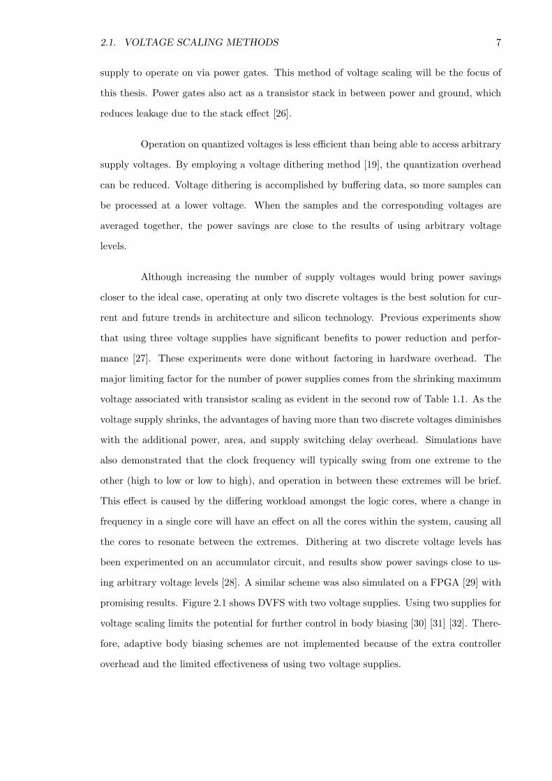
promising results. Figure 2.1 shows DVFS with two voltage supplies. Using two supplies for
voltage scaling limits the potential for further control in body biasing [30] [31] [32]. There-
fore, adaptive body biasing schemes are not implemented because of the extra controller
overhead and the limited effectiveness of using two voltage supplies.
8 CHAPTER 2. VOLTAGE SCALING
VddHigh
VddLowDVFScircuit
osc clk
VddCore
VddOn
Core Logic
Figure 2.1: Dynamic voltage and frequency scaling with two voltage supplies. The DVFScircuit is powered by an “always on” power supply called V ddon. Depending on the logicto the power gates, the core logic can operate on the high or low voltage supply, or becompletely shut off from power. The body of the PMOS gate of the low voltage supply istied to the high voltage supply to prevent a forward biased diode from drain to body.
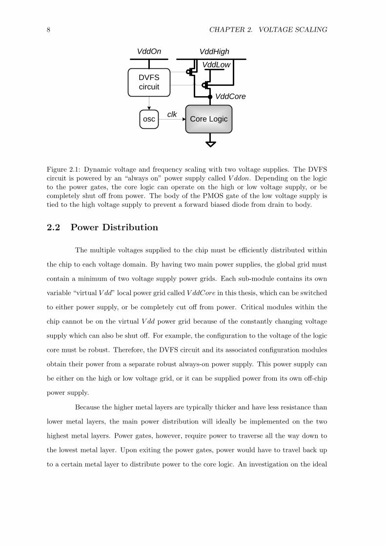
2.2 Power Distribution
The multiple voltages supplied to the chip must be efficiently distributed within
the chip to each voltage domain. By having two main power supplies, the global grid must
contain a minimum of two voltage supply power grids. Each sub-module contains its own
variable “virtual V dd” local power grid called V ddCore in this thesis, which can be switched
to either power supply, or be completely cut off from power. Critical modules within the
chip cannot be on the virtual V dd power grid because of the constantly changing voltage
supply which can also be shut off. For example, the configuration to the voltage of the logic
core must be robust. Therefore, the DVFS circuit and its associated configuration modules
obtain their power from a separate robust always-on power supply. This power supply can
be either on the high or low voltage grid, or it can be supplied power from its own off-chip
power supply.
Because the higher metal layers are typically thicker and have less resistance than
lower metal layers, the main power distribution will ideally be implemented on the two
highest metal layers. Power gates, however, require power to traverse all the way down to
the lowest metal layer. Upon exiting the power gates, power would have to travel back up
to a certain metal layer to distribute power to the core logic. An investigation on the ideal

2.3. POWER GATE DESIGN 9
metal layer for power distribution reveals that metals three and four are sufficient for power
distribution to the variable local grid for a 130nm technology [32]. Using lower layers for
power distribution reduces the resistance overhead associated with traversing through vias
to different metal layers. However, this approach is not adequate to effectively distribute
power if the DVFS circuit is designed as a wrapper. The logic core requires metals three and
four for routing; forcing the sub-module to route without using these layers will increase
area and decrease performance. Therefore, for a wrapper design, the best approach to
distribute power to the variable local grid is by using the top layers of metal.
2.3 Power Gate Design
The main interface between the logic core and the power supply is through the
power gates. PMOS gates are ideal for the power gate design because the body of the gates
are isolated within their own n-well. This is in contrast to the body connection of NMOS
gates, which are connected to the substrate in common single well CMOS processes. The
connection of the power gates to the substrate disallows two different biases to the body
of the NMOS gates (which is needed because for a PMOS design, where the body of the
PMOS gates are always connected to the higher voltage supply). PMOS power gates are
used in this thesis. By connecting the body of the power gate on the low voltage gates to
the high voltage supply, a potential forward bias diode between the drain and the body is
avoided [28].
The power gate design is based on the standard cell layout design within the
standard cell library to simplify the design flow. The same dimensions and layers from the
standard cell library were used for the design of the power gate. Because the layouts are
similar, design rule errors resulting from placing a custom built cell next to standard cells
are reduced. Figure 2.2 defines the basic structure of a power gate design. By aligning the
power gate dimension to match the width of the three power stripes, routing complexity
is reduced as power can go directly down to the gate through a series of vias. The PMOS
gates themselves occupy only about half of the total power gate area; the rest of the area
is devoted to having an abundant amount of metal vias, which reduces the resistance of
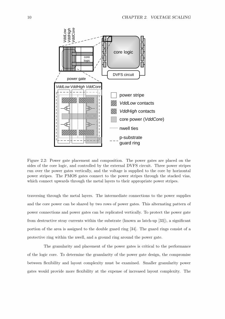
10 CHAPTER 2. VOLTAGE SCALING
core logic
DVFS circuit
Vdd
Low
Vdd
Hig
hV
ddC
ore
power gate
VddHighVddLow VddCore
power stripe
VddLow contacts
VddHigh contacts
core power (VddCore)
nwell ties
p-substrate guard ring
core logic
Figure 2.2: Power gate placement and composition. The power gates are placed on thesides of the core logic, and controlled by the external DVFS circuit. Three power stripesrun over the power gates vertically, and the voltage is supplied to the core by horizontalpower stripes. The PMOS gates connect to the power stripes through the stacked vias,which connect upwards through the metal layers to their appropriate power stripes.
traversing through the metal layers. The intermediate connections to the power supplies
and the core power can be shared by two rows of power gates. This alternating pattern of
power connections and power gates can be replicated vertically. To protect the power gate
from destructive stray currents within the substrate (known as latch-up [33]), a significant
portion of the area is assigned to the double guard ring [34]. The guard rings consist of a
protective ring within the nwell, and a ground ring around the power gate.
The granularity and placement of the power gates is critical to the performance
of the logic core. To determine the granularity of the power gate design, the compromise
between flexibility and layout complexity must be examined. Smaller granularity power
gates would provide more flexibility at the expense of increased layout complexity. The
2.4. PERFORMANCE OVERHEAD 11
largest possible granularity is to design a single power gate for each power supply. However,
a single source of power will result in current crowding issues as well as a massive IR drop for
transistors distant to the power gates [32]. Most sleep transistor designs distribute power
with many smaller power gates within the logic core [32] [35]. By placing power gates near
critical cells, the performance of the logic core will improve. However, the design will no
longer have a straight-forward layout flow, and the core will not be interchangeable. By
placing the power gates on the wrapper of the core logic, the core can be easily replaced
with another logic unit. The wrapper design employs power gates on the sides of the logic
core, as shown in Figure 2.2. The power gates are positioned in a vertical fashion so that
the power gates are aligned with the vertical power stripes. Power gates placed along the
top and bottom edges of the logic core can also be implemented. Depending on the size of
the logic core, this method might be unnecessary because it adds to the layout complexity
without substantially benefiting power distribution, as in the case of AsAP. For larger cores,
providing power from the top and bottom edges can further assist with decreasing IR drop.
2.4 Performance Overhead
Using a power gate design will result in a significant performance overhead. The
power gates act as resistors, so whenever current is sourced from the power supply, voltage
drop occurs across the power gates [36]. The amount of voltage drop is related to the
dimensions of the power gates:
VPG = IPGRPG ∝L
W(2.1)
where IPG is the current across the power gates, and RPG is its resistance, which is pro-
portional to the length L over width W . Because of this voltage drop, the logic core will
operate on a lower than ideal voltage, which will negatively impact transistor performance.
This phenomenon is demonstrated by the following equation, where the voltage drop across
the power gate (VPG) increases the gate delay (tPGd ) [35]:
tPGd ∝ V dd− VPG
V dd− VPG − Vt(2.2)
12 CHAPTER 2. VOLTAGE SCALING
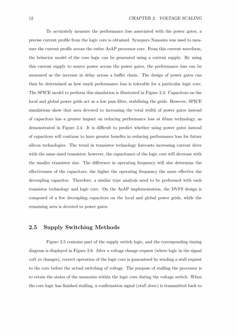
To accurately measure the performance loss associated with the power gates, a
precise current profile from the logic core is obtained. Synopsys Nanosim was used to mea-
sure the current profile across the entire AsAP processor core. From this current waveform,
the behavior model of the core logic can be generated using a current supply. By using
this current supply to source power across the power gates, the performance loss can be
measured as the increase in delay across a buffer chain. The design of power gates can
then be determined as how much performance loss is tolerable for a particular logic core.
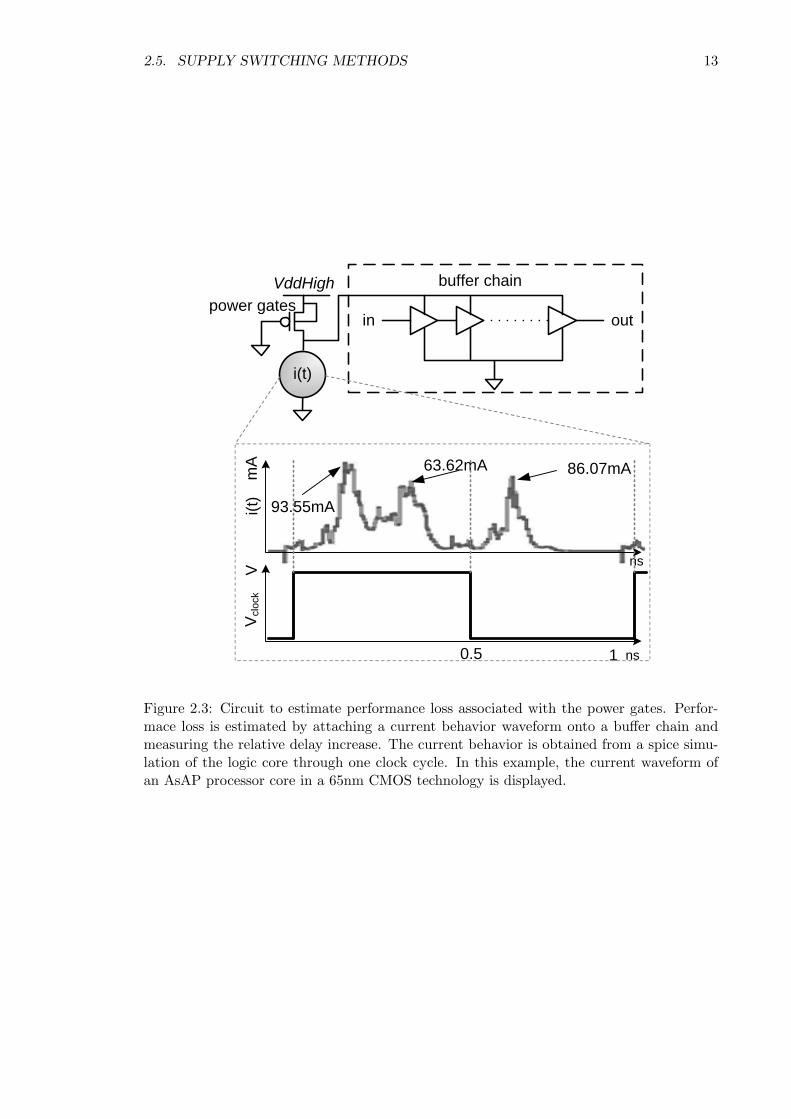
The SPICE model to perform this simulation is illustrated in Figure 2.3. Capacitors on the
local and global power grids act as a low pass filter, stabilizing the grids. However, SPICE
simulations show that area devoted to increasing the total width of power gates instead
of capacitors has a greater impact on reducing performance loss at 65nm technology, as
demonstrated in Figure 2.4. It is difficult to predict whether using power gates instead
of capacitors will continue to have greater benefits in reducing performance loss for future
silicon technologies. The trend in transistor technology forecasts increasing current drive
with the same sized transistor; however, the capacitance of the logic core will decrease with
the smaller transistor size. The difference in operating frequency will also determine the
effectiveness of the capacitors; the higher the operating frequency the more effective the
decoupling capacitor. Therefore, a similar type analysis need to be performed with each
transistor technology and logic core. On the AsAP implementation, the DVFS design is
composed of a few decoupling capacitors on the local and global power grids, while the
remaining area is devoted to power gates.
2.5 Supply Switching Methods
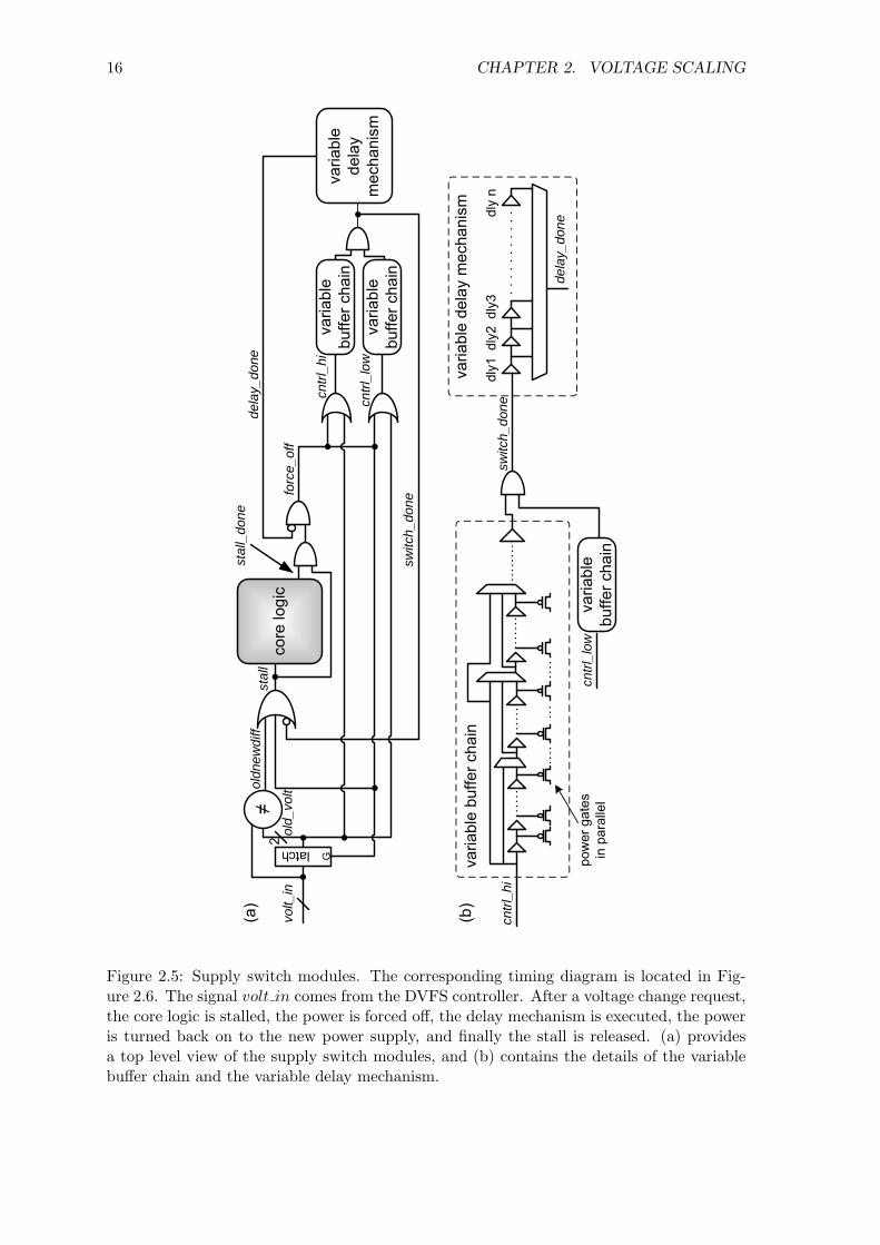
Figure 2.5 contains part of the supply switch logic, and the corresponding timing
diagram is displayed in Figure 2.6. After a voltage change request (where logic in the signal
volt in changes), correct operation of the logic core is guaranteed by sending a stall request
to the core before the actual switching of voltage. The purpose of stalling the processor is
to retain the states of the memories within the logic core during the voltage switch. When
the core logic has finished stalling, a confirmation signal (stall done) is transmitted back to
2.5. SUPPLY SWITCHING METHODS 13
VddHigh
in out
buffer chainpower gates
i(t)
mA
ns
nsV
93.55mA
63.62mA 86.07mA
0.5 1
i(t)
Vcl
ock
Figure 2.3: Circuit to estimate performance loss associated with the power gates. Perfor-mace loss is estimated by attaching a current behavior waveform onto a buffer chain andmeasuring the relative delay increase. The current behavior is obtained from a spice simu-lation of the logic core through one clock cycle. In this example, the current waveform ofan AsAP processor core in a 65nm CMOS technology is displayed.
14 CHAPTER 2. VOLTAGE SCALING
Figure 2.4: Comparison of performance loss vs ratio of area devoted to power gate widthand area devoted to decoupling capacitors. The experiment was performed using the circuitdiagram in Figure 2.3, and the total area for the power gates and decoupling capacitor was10% of the AsAP processor core area. For 65nm technology, the area devoted to the powergates have a greater impact on reducing performance loss.
2.6. COMMUNICATION ACROSS MULTIPLE VOLTAGE DOMAINS 15
the supply switch logic. Shorting between power supplies is prevented by first shutting off
power gates for both supplies (executed by the force off signal). A configurable amount
of delay is also provided between the switching of power supplies by the variable delay
mechanism. The variable delay mechanism is implemented with a simple delay chain and
a multiplexor, which can be initiated at various stages during the shut-off of power. Upon
completion of the delay, the force off signal is released by the delay done signal, and the
power gates are then turned on to the new power supply. Finally, the stall signal is released
once the logic has propagated to all the power gates. The method of shutting off or turning
on the power supply is configurable through the variable buffer chain. If performance is
critical, the voltage switching overhead can be reduced by configuring the power gates to
turn off and on instantly. Conversely, if the power grid noise is critical, the power gates
can be configured to turn off and on gradually. A low-slew-rate driving scheme for voltage
supply switching is the most effective method to combat power grid noise [37]. Too much
noise on the global supply affects the performance of neighboring sub-modules. The variable
buffer chain allows for an appropriate balance of performance and power grid noise with
the right configuration. A demonstration of the operation of the variable buffer chain with
its corresponding configuration is located in Figure 2.7.
2.6 Communication Across Multiple Voltage Domains
Communication across multiple voltage domains requires level shifters. A typical
level shifter involves a cross-coupled inverter with two voltage inputs [3]. Using this level
shifter complicates the layout process, because the gate needs access to both voltage sup-
plies. Instead, a four input NOR gate can be implemented on the communication between
the variable voltage logic core to the fixed voltage wrapper. The four input NOR gate
contains PMOSs in series and NMOSs in parallel, strengthening the pull down of the gate
and lowering the switching threshold voltage of the gate. During a 0 to 1 transition of the
gates of NOR transistors, the response of the 0 to Vddlow transition is sped up by the four
NMOS gates in parallel lowering the switching threshold. A 1 to 0 transition (Vddlow to
0) will operate like a gate without multiple voltage domains. One drawback of using these
16 CHAPTER 2. VOLTAGE SCALING
G
volt_
in
≠ol
d_vo
ltco
re lo
gic
stal
l
stal
l_do
ne
varia
ble
buffe
r cha
in
forc
e_of
f
oldn
ewdi
ff
varia
ble
dela
y m
echa
nism
varia
ble
buffe
r cha
in
dela
y_do
ne
cntrl
_hi
cntrl
_low
switc
h_do
necn
trl_h
i
switc
h_do
ne
pow
er g
ates
in
par
alle
l
latchva
riabl
e bu
ffer c
hain
dly1
dly2
dly3
dly
n
dela
y_do
ne
varia
ble
dela
y m
echa
nism
2
cntrl
_low
varia
ble
buffe
r cha
in
(a)
(b)
Figure 2.5: Supply switch modules. The corresponding timing diagram is located in Fig-ure 2.6. The signal volt in comes from the DVFS controller. After a voltage change request,the core logic is stalled, the power is forced off, the delay mechanism is executed, the poweris turned back on to the new power supply, and finally the stall is released. (a) providesa top level view of the supply switch modules, and (b) contains the details of the variablebuffer chain and the variable delay mechanism.
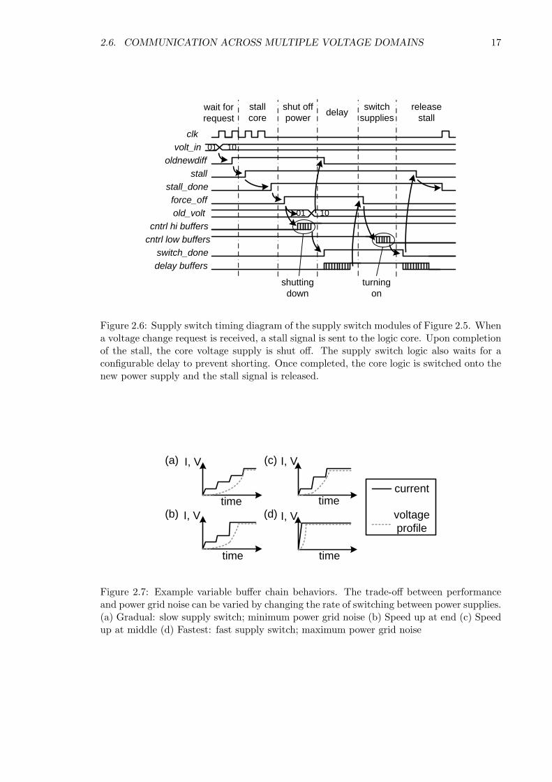
2.6. COMMUNICATION ACROSS MULTIPLE VOLTAGE DOMAINS 17
clkvolt_in
oldnewdiffstall
stall_doneforce_offold_volt
cntrl hi bufferscntrl low buffers
switch_donedelay buffers
01 10
01 10
wait for request
stall core
shut off power delay switch
suppliesrelease
stall
shutting down
turning on
Figure 2.6: Supply switch timing diagram of the supply switch modules of Figure 2.5. Whena voltage change request is received, a stall signal is sent to the logic core. Upon completionof the stall, the core voltage supply is shut off. The supply switch logic also waits for aconfigurable delay to prevent shorting. Once completed, the core logic is switched onto thenew power supply and the stall signal is released.
I, V
timeI, V
time
I, V
time
current
voltageprofile
I, V
time
(a)
(b)
(c)
(d)
Figure 2.7: Example variable buffer chain behaviors. The trade-off between performanceand power grid noise can be varied by changing the rate of switching between power supplies.(a) Gradual: slow supply switch; minimum power grid noise (b) Speed up at end (c) Speedup at middle (d) Fastest: fast supply switch; maximum power grid noise
18 CHAPTER 2. VOLTAGE SCALING
NOR gates is the static current across the partially shut-off PMOS gates when input is
high. SPICE simulations show that at 65nm the static current is only slightly worse than a
cross-coupled inverter level shifter (using high VT transitors). Only processor output ports
require level shifters for the cases of communicating from a low voltage domain to a higher
voltage domain.
2.7 Fail-safe Methods
Because the DVFS circuit determines the appropriate voltage supplied to the logic
core, adequate fail-safe methods must be implemented to ensure that the correct voltage
is adequately supplied. The power gate interface contains a force configuration mode that
overrides any inputs to the power gates.
When the DVFS circuit is not needed or is faulty, the logic core can be supplied
power from both high and low voltage power gates on the same voltage supply. This method
could effectively double the drive of the power gates and reduce the performance overhead.
19
Chapter 3
Dynamic Voltage and Frequency
Scaling Controller
The DVFS controller must be extremely configurable and flexible because different
configurations work better for different applications depending on the characteristics of its
workload. By providing a highly configurable circuit, flexibility is improved at the cost of
an increase in area and power. Flexibility of the DVFS circuit is achieved through a high
level configurability approach, where the configuration of a few bits leads to a significant
impact on behavior. Using a few bits for configuration simplifies the configuration procedure
while reducing the area and power overhead. Although high level configurability is not as
optimal as a lower level approach, the inherent characteristics of a multiple core architecture
eventually level out the non-optimal configurations across domains. The DVFS circuit and
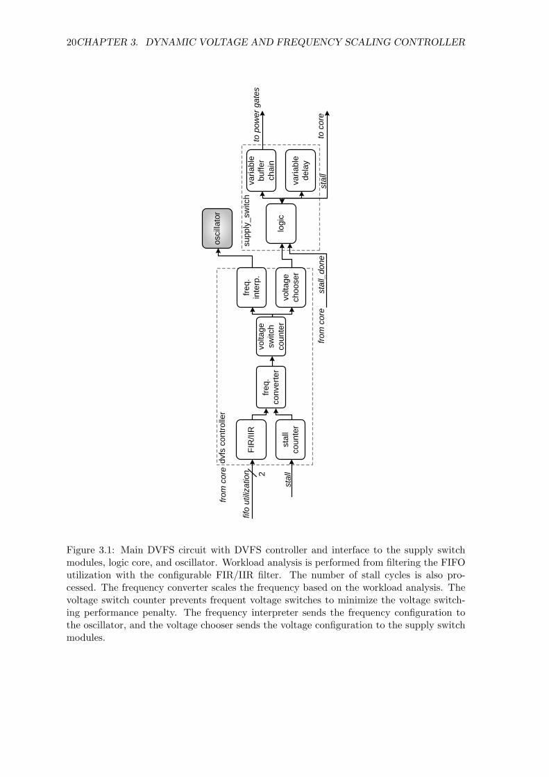
its associated modules are pictured in Figure 3.1.
3.1 Workload Analysis
Scaling frequency and voltage involves dynamically analyzing the workload for
each logic core.
1. Examining the state of an input FIFO is a possible approach to analyzing work-
loads [19]. When applied to a multiple voltage and frequency domain architecture,
20CHAPTER 3. DYNAMIC VOLTAGE AND FREQUENCY SCALING CONTROLLER
from
cor
edv
fs c
ontro
ller
volta
ge
switc
h co
unte
r
freq.
in
terp
.
volta
ge
choo
ser
osci
llato
r
logi
c
varia
ble
buffe
r ch
ain
varia
ble
dela
y
freq.
co
nver
ter
stal
l co
unte
r
FIR
/IIR
fifo
utili
zatio
n
stal
l
supp
ly_s
witc
h
from
cor
est
all_
done
to p
ower
gat
es
to c
ore
stal
l
2
Figure 3.1: Main DVFS circuit with DVFS controller and interface to the supply switchmodules, logic core, and oscillator. Workload analysis is performed from filtering the FIFOutilization with the configurable FIR/IIR filter. The number of stall cycles is also pro-cessed. The frequency converter scales the frequency based on the workload analysis. Thevoltage switch counter prevents frequent voltage switches to minimize the voltage switch-ing performance penalty. The frequency interpreter sends the frequency configuration tothe oscillator, and the voltage chooser sends the voltage configuration to the supply switchmodules.
3.1. WORKLOAD ANALYSIS 21
the utilization of a FIFO is an indication of the speed of a domain relative to other
domains.
2. The core logic stall period can also provide information about the workload. Long
idle periods indicates a low workload associated with that voltage domain.
3. Prediction of the workload can be accomplished by observing the instructions within
the instruction register. Using that information, however, does not guarantee a good
mapping to workload. When heterogeneous logic cores are used, the instruction set
may change, making the DVFS controller less portable.
4. The state of the FIFOs of neighboring domains can also be examined, but an increase
in interconnect and logic complexity does not make the technique feasible.
5. Static workload analysis presents workload and delay information, which can then be
used to generate algorithms for placing reconfiguration instructions [38] [39] [40] [41].
Adding reconfiguration instructions of frequency and voltage can be achieved through
a software interface. This method is not as effective as scaling the voltage and fre-
quency dynamically because of the performance overhead of decoding the reconfig-
uration instruction. Static analysis also may not be able to predict data-dependent
changes in workload.
The DVFS logic examines workload through the FIR/IIR filter and the stall counter modules
in Figure 3.1.
Increasing the sampling frequency will improve the accuracy of the workload anal-
ysis, at the expense of a higher power consumption. The optimal sampling frequency
depends on the workload characteristics of the application. If the DVFS controller contains
its own clock domain, adjustment of the clock frequency can alter the sampling rate. The
DVFS logic can also be clocked from the oscillator of the logic core. Adequate divisions
of the oscillator clock must be performed to ensure the low power operation of the DVFS
controller.
The filtering algorithm of the workload can have a significant impact on the per-
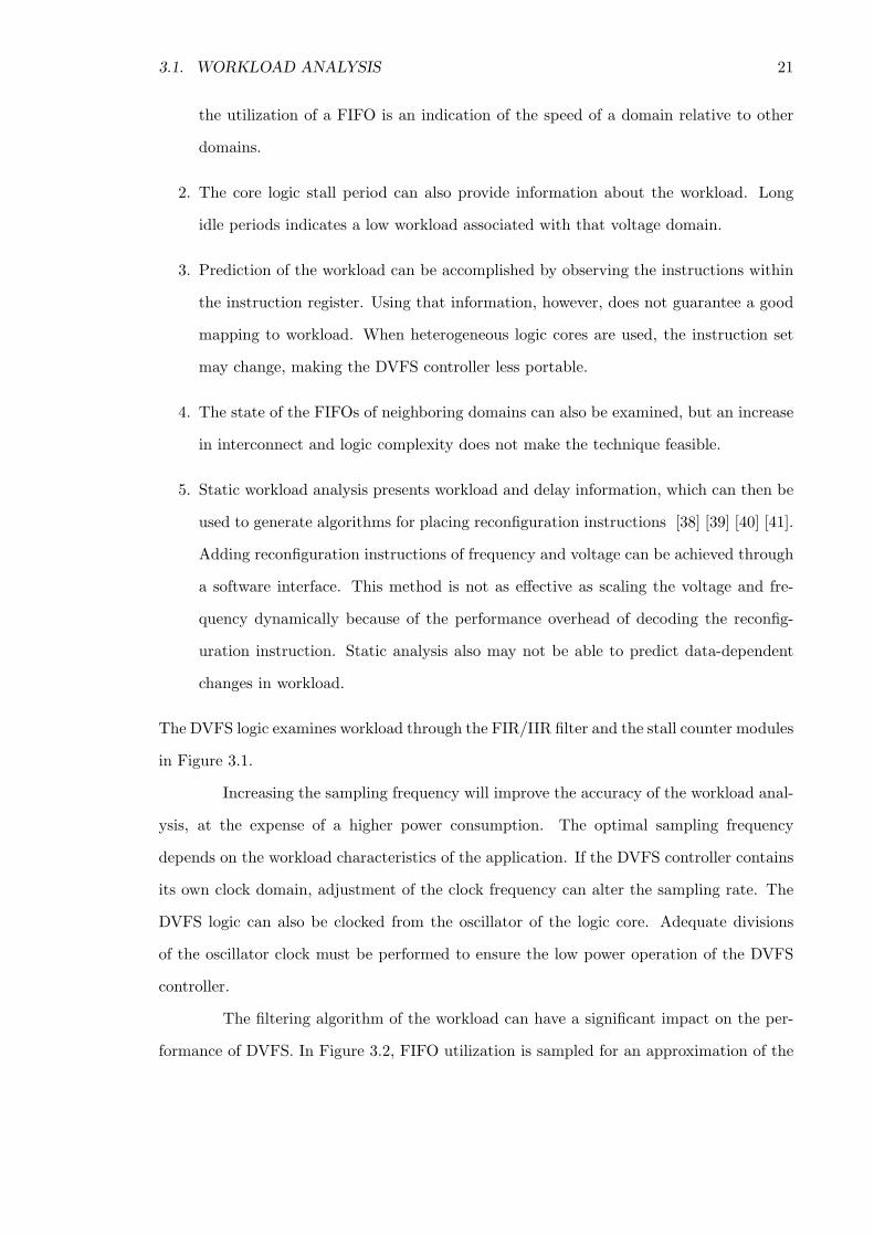
formance of DVFS. In Figure 3.2, FIFO utilization is sampled for an approximation of the
22CHAPTER 3. DYNAMIC VOLTAGE AND FREQUENCY SCALING CONTROLLER
11
10
01
00
FIFO
2
util
fir_out[3:2]
Figure 3.2: An example configuration of a 5 point adjustable FIR/IIR filter. The top twobits are taken from the fifo utilization. The FIR is adjustable through repeated inputs, andthe IIR feature is added through feedback of the adder.
workload, and the utilization can be approximated to four sections that can be described
with two bits to simplify the circuit. Methods of filtering workload has been investigated
in numerous literatures:
1. A moving average of the samples provides a good approximation of the workload [19].
2. By analyzing static workloads, it appears that a weighted average provides better
workload analysis than using data from the immediate past [38].
3. A global weighted average provides the best workload analysis [39].
A simple five point adjustable FIR/IIR filter can be used to analyze workload if the FIFO
utilization is described with two bits, as illustrated in Figure 3.2. Depending on the config-
uration, the filter design could exhibit characteristics of an FIR or IIR filter. The FIR filter
is used to provide an estimation of the local weighted average by storing information of the
recent past. The IIR filter is used to approximate the global behavior, which is achieved
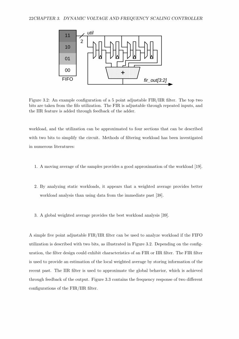
through feedback of the output. Figure 3.3 contains the frequency response of two different
configurations of the FIR/IIR filter.
3.1. WORKLOAD ANALYSIS 23
0 pi/4 pi/2 3pi/4 pi0
0.2
0.4
0.6
0.8
1
Angular Frequency(ω)
Nor
mal
ized
Mag
nitu
de H
e(jω)
FIRIIR
Figure 3.3: Frequency response of the DVFS filter. ω = π corresponds to fsample/2, wherefsample is adjustable. Solid line: Configuration 1110: 5 tap FIR filter Dashed line: Config-uration 0111: 3 tap IIR filter.
24CHAPTER 3. DYNAMIC VOLTAGE AND FREQUENCY SCALING CONTROLLER
3.2 Frequency Scaling
At the completion of the data filtering, workload information is converted to
changes on the frequency and voltage. Mapping the FIFO utilization to workload is the
most direct method of conversion. However, this technique does not provide enough flexi-
bility between the range of operable frequencies. Instead, the frequency can be incremented
or decremented based on the workload analysis. This is performed in the frequency convert
module in Figure 3.1. Configurability can be implemented through decisions of whether to
increment or decrement based on the FIFO utilization. Sensitivity to the workload is config-
ured by allowing only certain workloads to scale the frequency. Incremental or decremental
preference is configured by configuring more of the workload data to cause an increase or de-
crease in frequency. Configuration of the incremental step size is another option for scaling
frequency. However, this configuration scheme is not feasible because of the limited range of
operable frequencies, which will continue shrinking as supply voltage decreases with future
technologies.
3.3 Voltage Scaling
Frequency scaling and voltage scaling are well related processes. The two voltage
supplies will each be assigned with a range of operable frequencies. By providing a maximum
frequency on the high and low voltage supplies, data validity is guaranteed with DVFS.
Even equivalent circuits on different voltage domains require configurable valid operating
frequencies because of process variations. The minimum frequency on the high voltage
supply indicates a transition point between the high supply to the low supply. Similarly,
the maximum frequency of the low supply is a transition point to the high supply. The
minimum frequency on the low supply allows for the configuration of the desired alloted
frequency range on the voltage supplies. For example, configuring the minimum frequency
on the low supply to be close to the maximum frequency of the low supply, the frequency
range on the low supply will be small and the circuit will transition quicker to the high
supply. Similarly, configuring the minimum frequency to be further will cause the frequency
range to be larger and it will be more difficult for the circuit to transistion ot the high supply.
3.3. VOLTAGE SCALING 25
frequencyvo
ltage
low voltage
high voltage
voltage switch
operable frequency
configurable maximum/minimum frequency
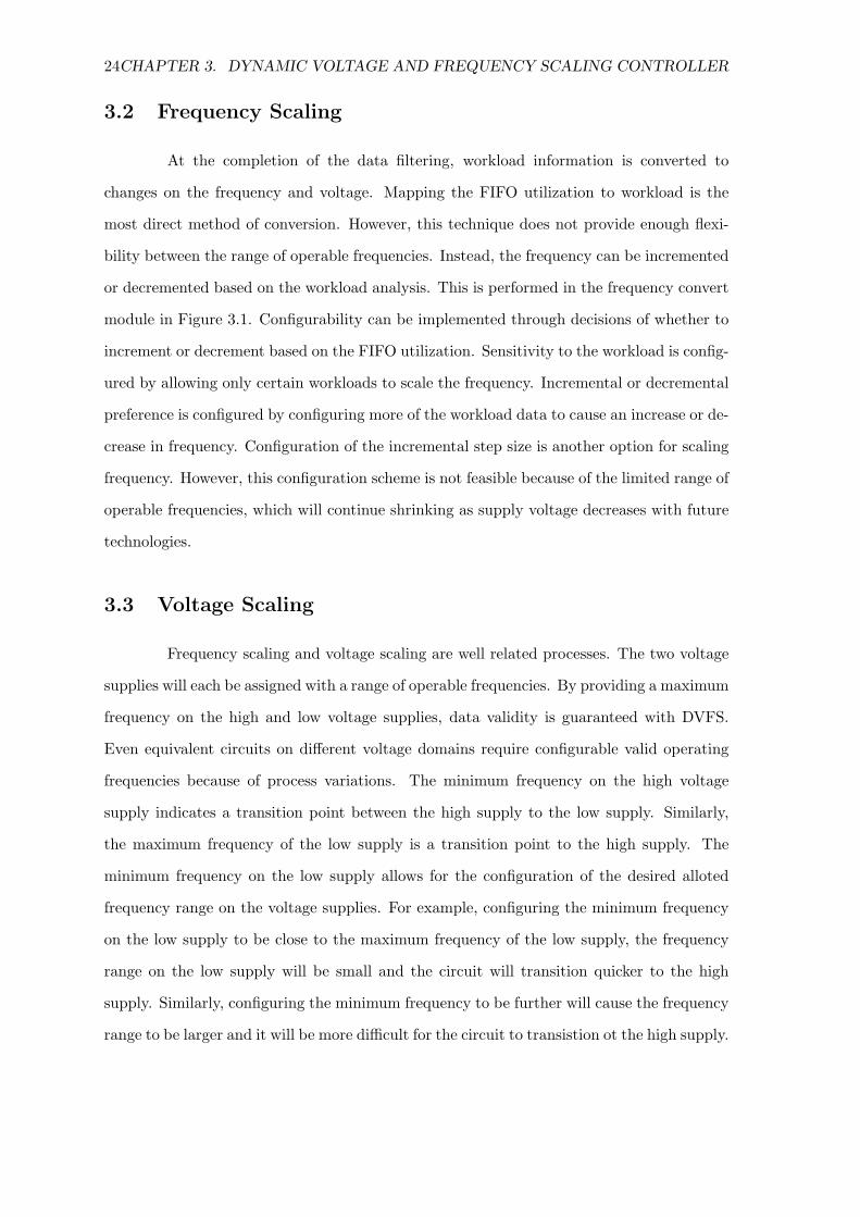
Figure 3.4: An example of the range of operable frequencies with its corresponding voltagesupplies. Two maximum and two minimum frequencies for the two voltage supplies areneeded for each voltage domain. The maximum frequencies prevent operation outside ofmaximum frequency for the voltage supply. The minimum frequencies can be used to setthe preference of operating on either supply.
Figure 3.4 demonstrates the configuration of the range of operable frequencies on the two
voltage supplies. Frequency scaling is frozen during a voltage transition, preventing the
frequency from exceeding the operable frequency range.
Switching between voltage supplies results in numerous clock cycle delays as ev-
ident in Figure 2.6. Cases where the core logic resonates between voltage supplies can be
detrimental to performance. The voltage switch counter in Figure 3.1 helps to resolve this
problem. After every voltage switch, this module counts a configurable number of clock
cycles before another voltage switch is permitted.

26
Chapter 4
Hardware Implementation
4.1 Voltage Scaling Details
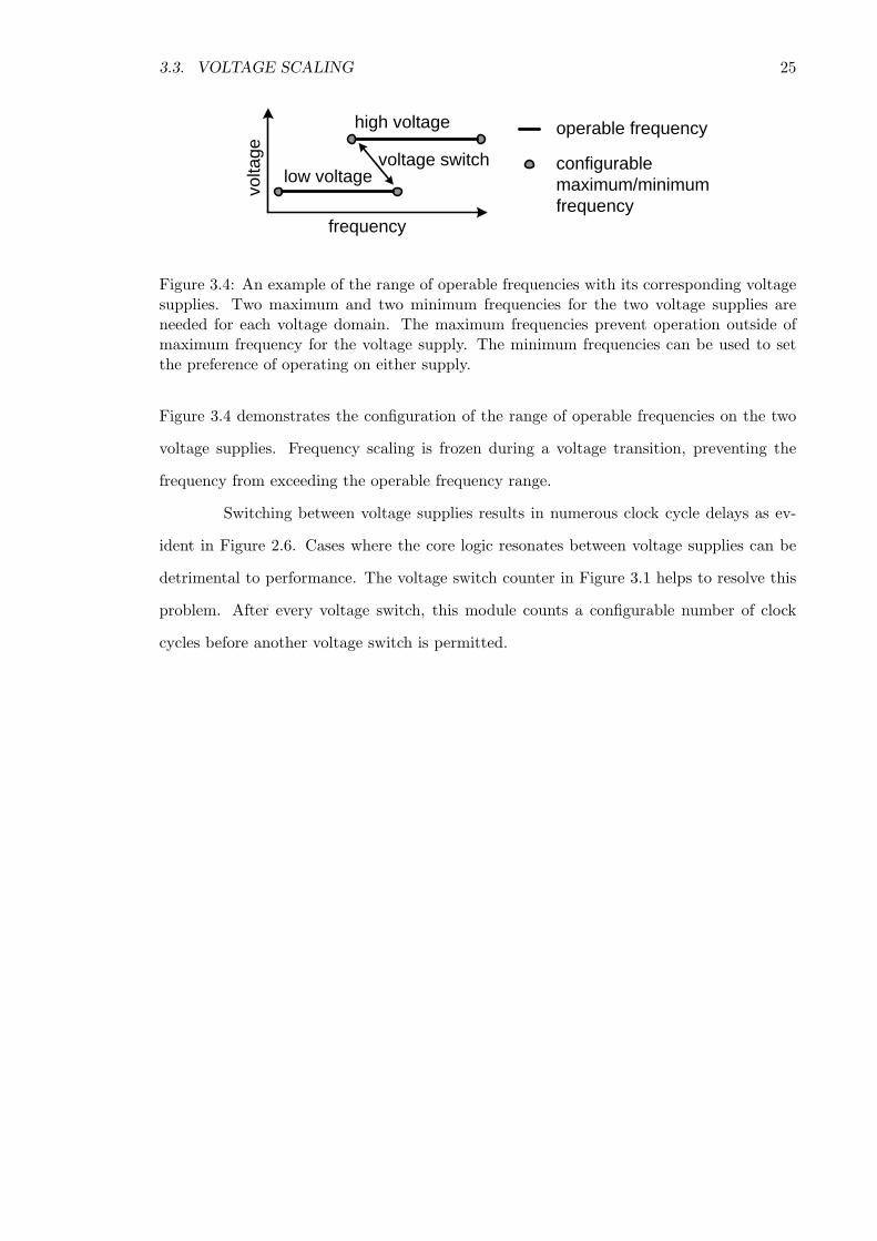
The detailed logic portion of the supply switch module is shown in Figure 4.1.
There are three modes of operation:
1. The normal operation mode switches from one voltage supply to the other, while
stalling the processor during the voltage switch.
2. The stall disabled mode bypasses the portion in the logic that sends the stall signal
to the processor.
3. The shutdown to turn on mode only activates when the processor is shut down and
wants to turn back on. The timing diagram of all three modes are shown in Figure 4.2.
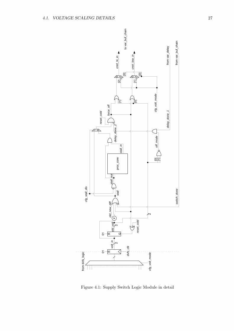
The variable buffer chain is shown in Figure 4.3. It contains four smaller interme-
diate variable buffer chains shown in the bottom picture of Figure 4.3. Each intermediate
variable buffer chain controls twelve power gates. The variable buffer chain controls a total
of 48 power gates on each voltage supply.
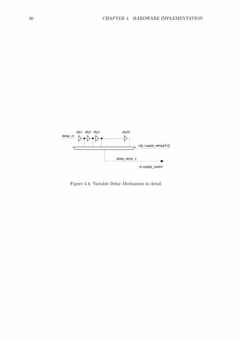
The variable delay mechanism is shown in Figure 4.4. The delay sequence can
be started by either the signal prior to entering the variable delay buffers(first buf), the
signal half way through the buffers(half buf), or the signal exiting buffers(last buf).
The configurations for the supply switch modules are shown in Table 4.1.
4.1. VOLTAGE SCALING DETAILS 27
from
dvf
s_lo
gic
dvfs
_clk
cfg_
volt_
mod
e
volt_
in
01 GR
01 R
≠old_
new
_diff
stal
l
cfg_
stal
l_di
s
stal
l_ou
t
proc
_cor
est
all_
in
1 0re
set_
cold
rese
t_co
ld
forc
e_of
fol
d_vo
lt2
2
2
[0]
[1]
off_
mod
e
[0]
[1]
0 1 0 1
cfg_
volt_
mod
e
[0]
[0]
[1]
[2]
cntrl
_hi_
in
cntrl
_low
_in
to v
ar_b
uf_c
hain
dela
y_do
ne_1
from
var
_del
ay
dela
y_do
ne_2
switc
h_do
nefro
m v
ar_b
uf_c
hain
Figure 4.1: Supply Switch Logic Module in detail

28 CHAPTER 4. HARDWARE IMPLEMENTATION
clk
volt_
in
oldn
ewdi
ff
stal
l_ou
t
stal
l_in
forc
e_of
f
old_
volt
cntrl
_hi_
in
cntrl
_low
_in
last
bufh
i
last
buflo
w
dela
yin
dela
ydon
e
switc
hdon
e
0110
0110
Nor
mal
Ope
ratio
n
clk
volt_
in
oldn
ewdi
ff
stal
l_ou
t
forc
e_of
f
old_
volt
cntrl
_hi_
in
cntrl
_low
_in
last
bufh
i
last
buflo
w
dela
yin
dela
ydon
e
switc
hdon
e
0110
0110
Sta
ll D
isab
led
clk
volt_
in
oldn
ewdi
ff
stal
l_ou
t
stal
l_in
forc
e_of
f
old_
volt
cntrl
_hi_
in
cntrl
_low
_in
last
bufh
i
last
buflo
w
dela
yin
dela
ydon
e2
switc
hdon
e0111
0111
Shut
dow
n →
Turn
On
dela
ydon
e1
01
01
(a)
(b)
(c)
Figure 4.2: Supply Switch Timing in detail
4.1. VOLTAGE SCALING DETAILS 29
cfg_
var_
buf_
hi
[7]
cntrl
_hi
from
sup
ply_
switc
h
var_
buf
_int
er
2 1 0
1
[9:8
]
var_
buf
_int
er
1
[11:
10]3 2 1 0
var_
buf
_int
er
1
[13:
12]3 2 1 0
var_
buf
_int
er
cfg_
var_
buf_
low
[7]
cntrl
_low
var_
buf
_int
er
2 1 0
1
[9:8
]
var_
buf
_int
er
1
[11:
10]3 2 1 0
var_
buf
_int
er
1
[13:
12]3 2 1 0
var_
buf
_int
er
first
_buf
half_
buf
last
_buf
0 1 2
cfg_
supp
ly_d
elay
[6:5
]
dela
y_in
to v
ar_d
elay
switc
h_do
ne
to s
uppl
y_sw
itch
[0]
cfg_
var_
buf_
x
2 1 0cn
trl_x
_in
1
[2:1
]
3 2 1 0
1
[4:3
]
3 2 1 0
1
cntrl
_x_o
ut
[6:5
]
(a)
(b)
Figure 4.3: Variable Buffer Chain in detail
30 CHAPTER 4. HARDWARE IMPLEMENTATION
delay_in
delay_done_1
to supply_switch
dly1 dly2 dly3 dly32
cfg_supply_delay[4:0]
Figure 4.4: Variable Delay Mechanism in detail
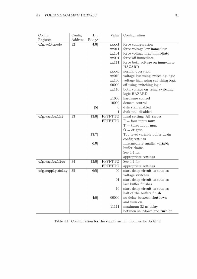
4.1. VOLTAGE SCALING DETAILS 31
Config Config Bit Value ConfigurationRegister Address Rangecfg volt mode 32 [4:0] xxxx1 force configuration
xx011 force voltage low immediatexx101 force voltage high immediatexx001 force off immediatexx111 force both voltage on immediate
HAZARDxxxx0 normal operationxx010 voltage low using switching logicxx100 voltage high using switching logic00000 off using switching logicxx110 both voltage on using switching
logic HAZARDx1000 hardware control10000 dcmem control
[5] 0 dvfs stall enabled1 dvfs stall disabled
cfg var buf hi 33 [13:0] FFFFTTO Ideal setting: All ZeroesFFFFTTO F = four input mux
T = three input muxO = or gate
[13:7] Top level variable buffer chainconfig settings
[6:0] Intermediate smaller variablebuffer chainsSee 4.4 forappropriate settings
cfg var buf low 34 [13:0] FFFFTTO See 4.4 forFFFFTTO appropriate settings
cfg supply delay 35 [6:5] 00 start delay circuit as soon asvoltage switches
01 start delay circuit as soon aslast buffer finishes
10 start delay circuit as soon ashalf of the buffers finish
[4:0] 00000 no delay between shutdownand turn on
11111 maximum 32 ns delaybetween shutdown and turn on
Table 4.1: Configuration for the supply switch modules for AsAP 2
32 CHAPTER 4. HARDWARE IMPLEMENTATION
4.2 Dynamic Voltage and Frequency Scaling Controller De-
tails
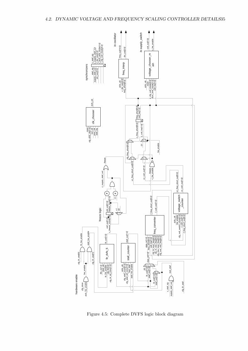
The DVFS controller block diagram is shown in Figure 4.5. In addition to the
internal modules, the DVFS controller also contains synchronizers for communicating across
unrelated clock domains, and freeze logic to prevent the frequency from changing during a
voltage change.
The FIR/IIR filter is shown in Figure 4.6. Workload is sampled by the top 2 bits
of the FIFO occupancy variable fifo util, and filtered based on the filter configuration.
The output of the filter can increase or decrease the frequency based on the bit convert
configuration cfg fir bit conv.
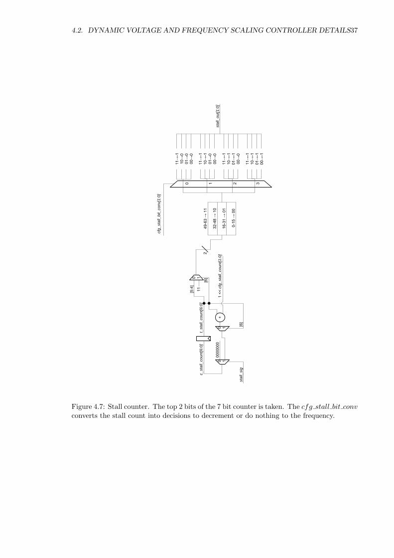
The stall counter is shown in Figure 4.7. The module counts the number of cycles
during the stall period, which then proceeds to decrease the frequency based on the state
of the counter.
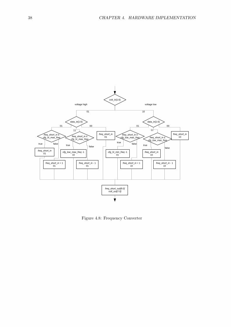
The frequency converter is best described by the flowchart shown in Figure 4.8.
There are two states in the flowchart: the voltage high and voltage low stages. The two
stages have different operations at the limits of their respective frequency ranges. The
converter also performs the increment and decrement of the frequency.
The voltage switch counter is located in Figure 4.9. The counter is best described
by the simplified state machine on the top right corner of the figure. A number of clock
cycles is counted following a voltage switch before a voltage switch is permitted again.
A concept diagram of the oscillator is shown in Figure 4.10 [16]. The oscillator
contains 9 stages, where each stage contains 7 tri-state inverters. The tri-state inverters
control the current drive of the ring oscillator; increasing the current drive means increasing
the clock frequency of the oscillator. Each stage of 7 tri-state inverters is controlled by three
control bits. The bottom 9 bits control 3 stages, where each stage is controlled by 3 bits.
The next 3 bits control two stages, and finally the last 3 bits control four stages. In addition
to the oscillator, the clock is then divided up to 128 times with 3 control bits.
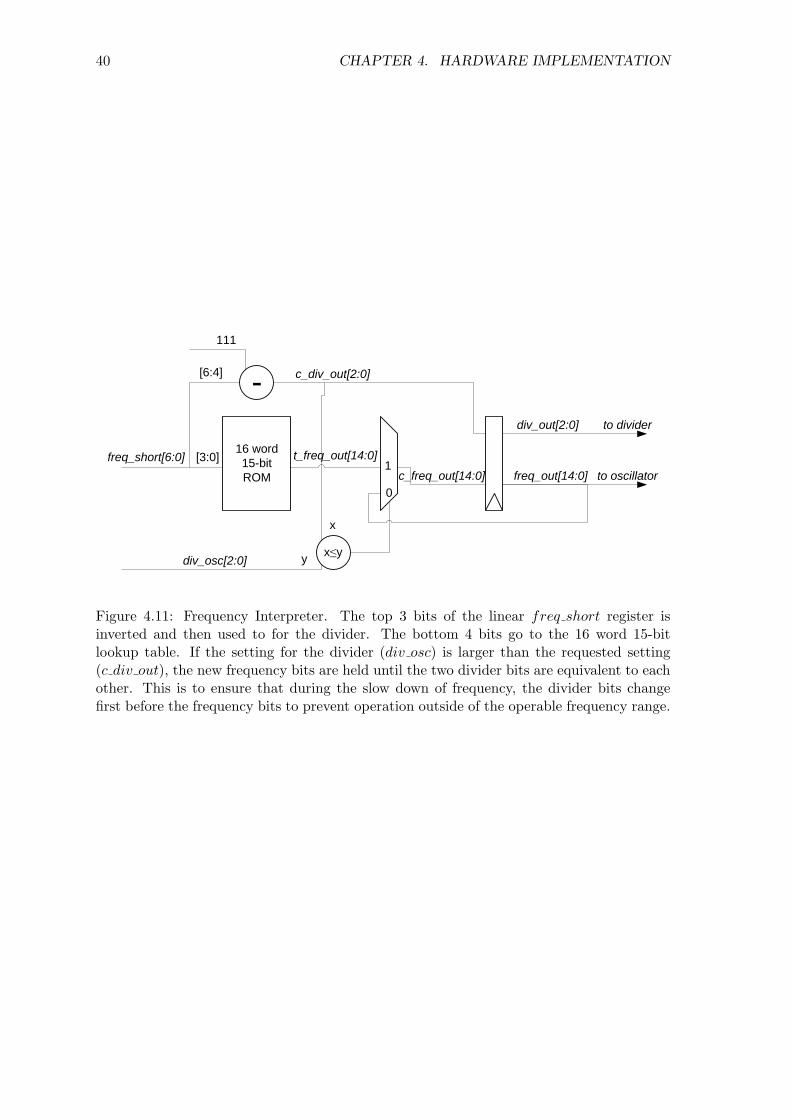
The frequency interpreter transforms a linear frequency register into configuration
bits for the oscillator. To map a linear frequency register to control 15 frequency bits and 3
4.2. DYNAMIC VOLTAGE AND FREQUENCY SCALING CONTROLLER DETAILS33
divider bits, the lower bits are used for the ring oscillator settings and the upper 3 bits are
used for the divider settings (so that overflow of the oscillator settings will configure the next
clock divider settings). In order to scale frequency in a linear fashion, the ring oscillator
needs to be characterized so that the delay interval between neighboring configurations
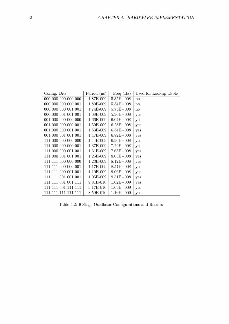
are similar. The ring oscillator is simulated using SPICE with hand picked configuration
settings that produce same delay intervals, and the results are shown in Table 4.2. A
16 word lookup table (controlled by 4 configuration bits) is used to send the appropriate
configuration settings to the oscillator (denoted in the rightmost column in Table 4.2). The
settings were picked so that the lowest ring oscillator setting can make a smooth transition
to the highest ring oscillator setting between clock divider stages. A safety mechanism is
developed to prevent the frequency settings to the ring oscillator from changing before the
clock has been successfully divided (which is accomplished by the simple comparator in
Figure 4.11). The 7 bit linear frequency register consists of the upper 3 bits controlling the
divider and the lower 4 bits referencing the lookup table. The diagram of the frequency
interpreter is shown in Figure 4.11.
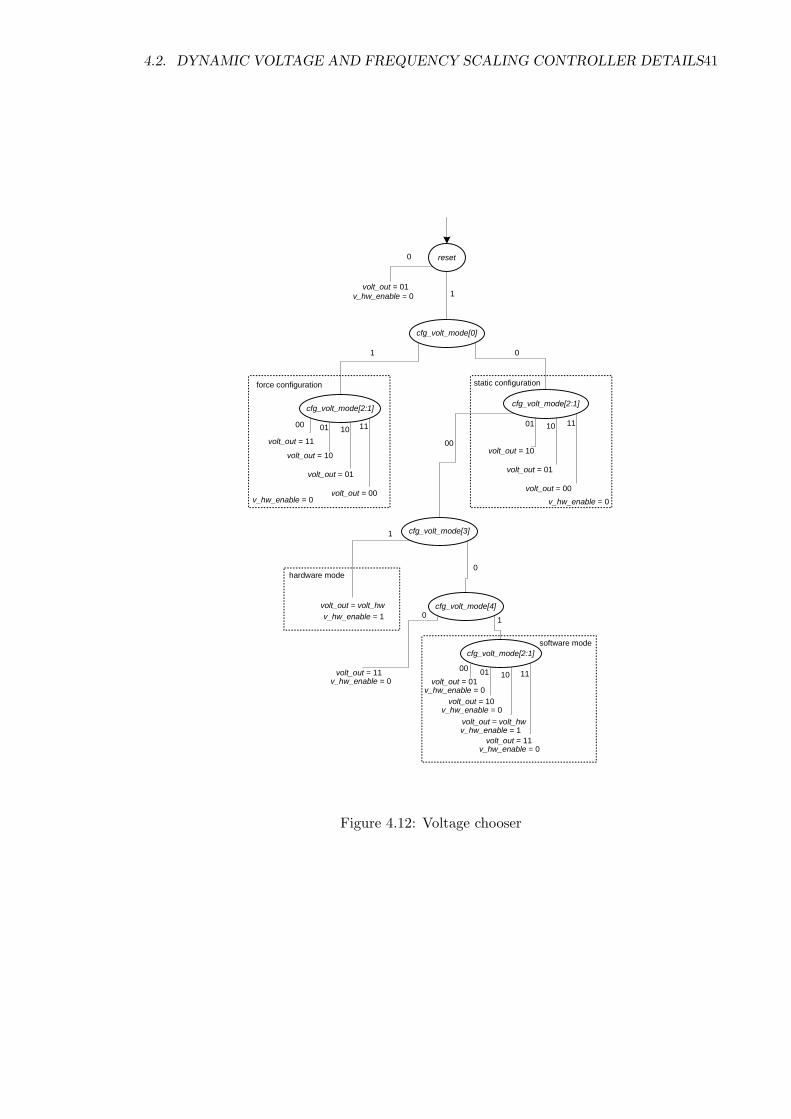
The voltage chooser module shown in Figure 4.12 decides which voltage to operate
on. There are four configuration modes: force configuration, static configuration, hardware,
and software.
1. The force configuration mode forces control bits to the power gates (see Figure 4.1).
2. The static configuration mode configures the power gates during the configuration
stage and has almost the same function as the force configuration mode.
3. The hardware mode allows the DVFS controller to scale frequency and voltage dy-
namically.
4. The software mode allows setting the frequency bits, divider bits, and voltage settings
with software instructions. The software configuration settings for frequency and
voltage scaling are shown in Table 4.6.
In addition to the variable voltage configuration schemes, the method of configur-
ing the frequency can also be changed. The settings are shown in Table 4.5.
34 CHAPTER 4. HARDWARE IMPLEMENTATION
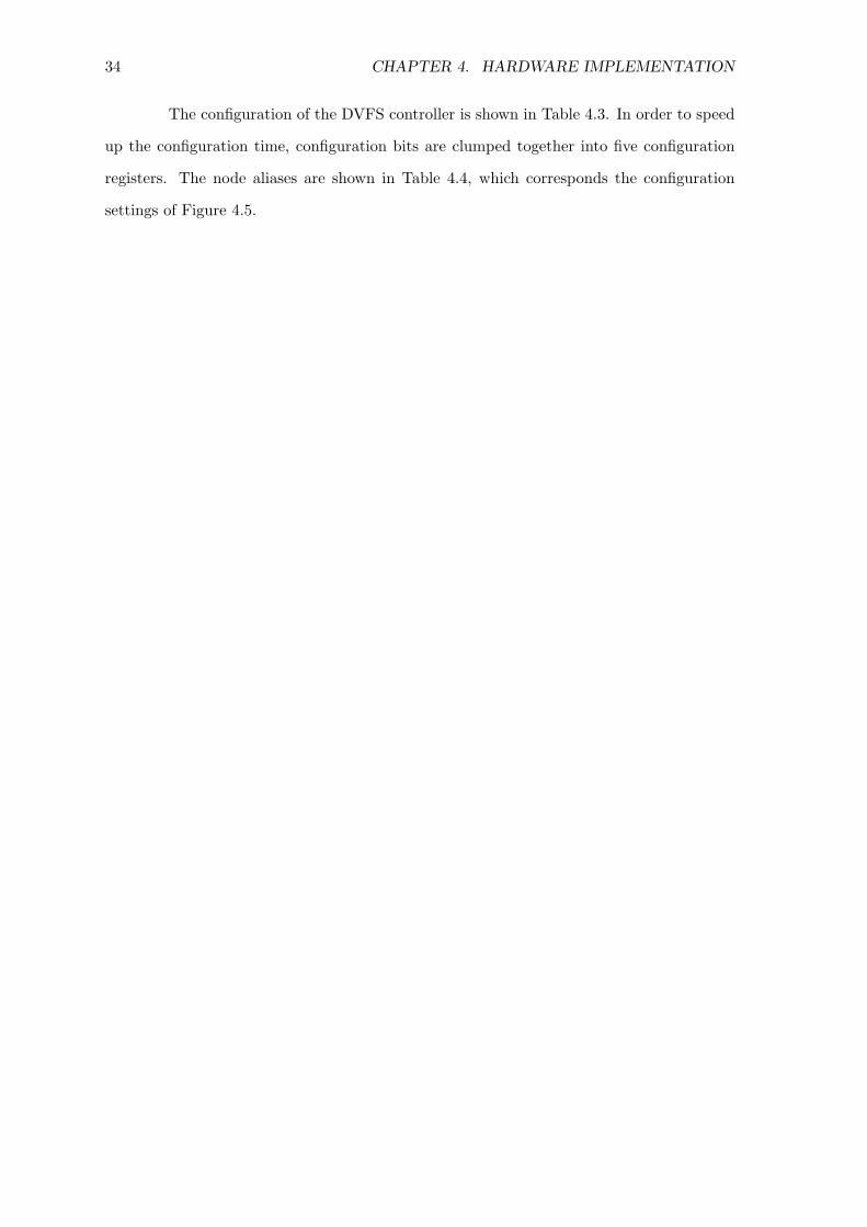
The configuration of the DVFS controller is shown in Table 4.3. In order to speed
up the configuration time, configuration bits are clumped together into five configuration
registers. The node aliases are shown in Table 4.4, which corresponds the configuration
settings of Figure 4.5.
4.2. DYNAMIC VOLTAGE AND FREQUENCY SCALING CONTROLLER DETAILS35
stal
l_si
gsu
pply
_sta
ll_ou
tdi
v_os
c[2:
0]
c_st
all_
sig
c_su
pply
_sta
ll_ou
tc_
div_
osc[
2:0]
c_dc
m_d
vfs_
mod
e[1:
0]c_
cfg_
volt_
mod
e[4:
0]
sync
hron
izer
s
fir_d
vfs_
5
fifo_
in[1
:0]
dvfs
_clk
fir_h
w_e
nabl
ecf
g_fir
[3:0
]cf
g_fir
_bit_
conv
[1:0
]
fir_o
ut[1
:0]
stal
l_co
unte
r
dvfs
_clk
cfg_
stal
l_co
unt[1
:0]
cfg_
stal
l_bi
t_co
nv[1
:0]
real
_sta
llst
all_
hw_e
nabl
e
stal
l_ou
t[1:0
]
hard
war
e en
able
cfg_
done
dvfs
_hw
_ena
ble
cfg_
fir_s
tall[
0]
cfg_
fir_s
tall[
1]
fir_h
w_e
nabl
e
stal
l_hw
_ena
ble
hw_e
nabl
e
freq_
conv
erte
r
data
_in[
1:0]
freq_
shor
t[6:0
]vo
lt_hw
[1:0
]cf
g_hi
_max
_fre
q[6:
0]cf
g_hi
_min
_fre
q[6:
0]cf
g_lo
w_m
ax_f
req[
6:0]
cfg_
low
_min
_fre
q[6:
0]
f_fre
q_sh
ort_
out[6
:0]
f_vo
lt_ou
t[1:0
]
0 1 2 3
00fir
_out
[1:0
]st
all_
out[1
:0]
0 1
fir_o
ut[1
:0]
stal
l_ou
t[1:0
]
data
_in[
1:0]
volta
ge_s
witc
h_c
ount
er
dvfs
_clk
hw_e
nabl
ecf
g_vo
lt_sw
itch_
coun
t[1:0
]f_
volt_
out[1
:0]
f_fre
q_sh
ort_
out[6
:0]
vc_f
req_
shor
t_ou
t[6:0
]
vc_v
olt_
out[1
:0]
hw_e
nabl
e
freq_
shor
t[6:0
]vo
lt_hw
[1:0
]c_
freq_
shor
t[6:0
]
c_vo
lt_hw
[1:0
]
freez
ev_
hw_e
nabl
e
0 1 0 1
vc_f
req_
shor
t_ou
t[6:0
]
vc_v
olt_
out[1
:0]
cfg_
freq_
shor
t[6:0
]0 1 0 1
01
freez
e lo
gic
volt_
out[1
:0]
c_fre
eze_
coun
t[1:0
]ol
d_vo
lt[1:
0]fre
eze_
coun
t[1:0
]
+1 00
≠ ≠11
c_su
pply
_sta
ll_ou
tfre
eze
0 1
freq_
inte
rpdv
fs_c
lkc_
div_
osc[
2:0]
freq_
shor
t[6:0
]
freq_
out[1
4:0]
div_
out[2
:0]
volta
ge_c
hoos
er_m
ain
dvfs
_clk
rese
tc_
cfg_
volt_
mod
e[4:
0]dc
m_d
vfs_
mod
e[1:
0]vo
lt_hw
[1:0
]
volt_
out[1
:0]
v_hw
_ena
ble
to o
scill
ator
to s
uppl
y_sw
itch
clk_
choo
ser
rese
tcf
g_dv
fs_c
lk[1
:0]
ext_
clk
proc
_clk
stal
l_si
g
dvfs
_clk
real
_sta
llc_
stal
l_si
g
supp
ly_s
tall_
out
cfg_
fir_s
tall
Figure 4.5: Complete DVFS logic block diagram

36 CHAPTER 4. HARDWARE IMPLEMENTATION
0 1
sam
pled
_dat
a[1:
0]
[0]
2
[2]
[3]
cfg_
fir[1
:0]
0 10 1
0 1
+
fir_o
ut[1
:0]
F I F O
49-6
4 →
11
32-4
8 →
10
16-3
1 →
01
0-15
→ 0
0
11→
110→
001→
000→
-1
11→
110→
101→
000→
-1
11→
110→
001→
-100→
-1
11→
110→
101→
-100→
-1
cfg_
fir_b
it_co
nv[1
:0]
t_fir
_out
[3:2
]
0 1 32
22
2
2
2
Figure 4.6: 5 point FIR/IIR filter. The top 2 bits of the utilization of the 64 bit FIFOis sampled as the workload. The cfg fir bit conv converts the two bits into decisions toeither increment, decrement, or do nothing to the frequency.
4.2. DYNAMIC VOLTAGE AND FREQUENCY SCALING CONTROLLER DETAILS37
0 10 1
stal
l_si
g
c_st
all_
coun
t[6:0
]t_
stal
l_co
unt[6
:0]
[6]
+1
<< c
fg_s
tall_
coun
t[1:0
]00
0000
0
[5:4
]0 1
[6]
11
stal
l_ou
t[1:0
]
11→
-110→
001→
000→
0
11→
-110→
-101→
000→
0
11→
-110→
-101→
-100→
0
11→
-110→
-101→
-100→
-1
cfg_
stal
l_bi
t_co
nv[1
:0]
49-6
3 →
11
32-4
8 →
10
16-3
1 →
01
0-15
→ 0
0
2
0 1 32
Figure 4.7: Stall counter. The top 2 bits of the 7 bit counter is taken. The cfg stall bit convconverts the stall count into decisions to decrement or do nothing to the frequency.
38 CHAPTER 4. HARDWARE IMPLEMENTATION
01
voltage high
01
11
00
true false true false
freq_short_in01
freq_short_in + 101
cfg_low_max_freq -110
freq_short_in - 101
freq_short_in01
01
11
00
true false truefalse
freq_short_in + 110
freq_short_in - 110
freq_short_in10
voltage low
10
cfg_hi_min_freq -101
freq_short_in10
freq_short_out[6:0]volt_out[1:0]
volt_in[1:0]
data_in[1:0] data_in[1:0]
freq_short_in ≥ cfg_hi_max_freq freq_short_in ≤
cfg_hi_max_freq
freq_short_in ≥ cfg_low_max_freq freq_short_in ≤
cfg_low_max_freq
Figure 4.8: Frequency Converter

4.2. DYNAMIC VOLTAGE AND FREQUENCY SCALING CONTROLLER DETAILS39
c_state state
c_volt_out[1:0] volt_out[1:0]
01
01
01
01
01
hw_enable
volt_in[1:0]
0
state
01
01
volt_out[1:0]
volt_in[1:0] ≠
volt_switch_count[6:5]
cfg_volt_switch_count[1:0] =
10
01
volt_out[1:0]
State Machine Circuit
volt_switch_count[6:0] c_volt_switch_count[6:0]
Voltage Switch Counter
01
01
+
hw_enable
0
1
0
state
Frequency Change Logic
old_freq_short[6:0] freq_short_out[6:0]
01
01
statevolt_out[1:0]
volt_in[1:0] =
fs_freq_short_in[6:0]
neutral state
voltage count state
voltage change
voltage change
count done
Simplified State Machine
Figure 4.9: Voltage Switch Counter
dec[0][1][2]
Tri-state inverter stage
1 2 3 4 5 6 7 8 9
01
2
34
5
67
8
910
11
1213
14
Figure 4.10: Simplified oscillator diagram
40 CHAPTER 4. HARDWARE IMPLEMENTATION
16 word 15-bit ROM
freq_short[6:0]
[6:4]
[3:0]
x
c_div_out[2:0]
t_freq_out[14:0]
c_freq_out[14:0]
x≤ydiv_osc[2:0]
freq_out[14:0]
div_out[2:0] to divider
to oscillator1
0
111
y
Figure 4.11: Frequency Interpreter. The top 3 bits of the linear freq short register isinverted and then used to for the divider. The bottom 4 bits go to the 16 word 15-bitlookup table. If the setting for the divider (div osc) is larger than the requested setting(c div out), the new frequency bits are held until the two divider bits are equivalent to eachother. This is to ensure that during the slow down of frequency, the divider bits changefirst before the frequency bits to prevent operation outside of the operable frequency range.
4.2. DYNAMIC VOLTAGE AND FREQUENCY SCALING CONTROLLER DETAILS41
reset
1
0
volt_out = 01v_hw_enable = 0
cfg_volt_mode[0]
cfg_volt_mode[2:1]
1
00 01 10 11
volt_out = 11
volt_out = 10
volt_out = 01
volt_out = 00v_hw_enable = 0
force configuration
cfg_volt_mode[2:1]
0
00
01 10 11
volt_out = 10
volt_out = 01
volt_out = 00
static configuration
cfg_volt_mode[3]
v_hw_enable = 0
1
volt_out = volt_hwv_hw_enable = 1
hardware mode
cfg_volt_mode[4]
0
cfg_volt_mode[2:1]
1
00 01 10 11volt_out = 01
volt_out = 10
volt_out = volt_hw
volt_out = 11
v_hw_enable = 0
v_hw_enable = 0
v_hw_enable = 1
v_hw_enable = 0
software mode
0
volt_out = 11v_hw_enable = 0
Figure 4.12: Voltage chooser
42 CHAPTER 4. HARDWARE IMPLEMENTATION
Config. Bits Period (ns) Freq (Hz) Used for Lookup Table000 000 000 000 000 1.87E-009 5.35E+008 no000 000 000 000 001 1.80E-009 5.54E+008 no000 000 000 001 001 1.74E-009 5.75E+008 no000 000 001 001 001 1.68E-009 5.96E+008 yes001 000 000 000 000 1.66E-009 6.04E+008 yes001 000 000 000 001 1.59E-009 6.28E+008 yes001 000 000 001 001 1.53E-009 6.54E+008 yes001 000 001 001 001 1.47E-009 6.82E+008 yes111 000 000 000 000 1.44E-009 6.96E+008 yes111 000 000 000 001 1.37E-009 7.29E+008 yes111 000 000 001 001 1.31E-009 7.65E+008 yes111 000 001 001 001 1.25E-009 8.03E+008 yes111 111 000 000 000 1.23E-009 8.12E+008 yes111 111 000 000 001 1.17E-009 8.57E+008 yes111 111 000 001 001 1.10E-009 9.06E+008 yes111 111 001 001 001 1.05E-009 9.51E+008 yes111 111 001 001 111 9.81E-010 1.02E+009 yes111 111 001 111 111 9.17E-010 1.09E+009 yes111 111 111 111 111 8.59E-010 1.16E+009 yes
Table 4.2: 9 Stage Oscillator Configurations and Results
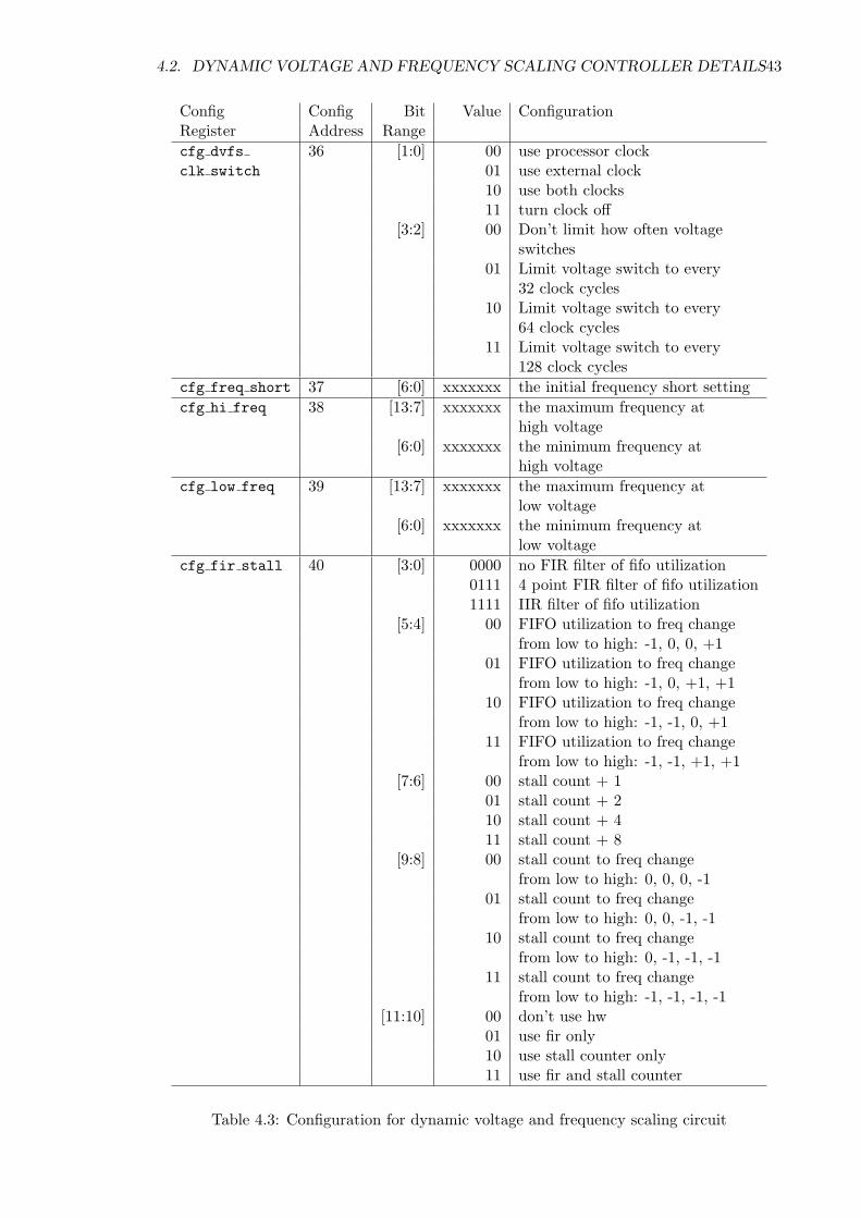
4.2. DYNAMIC VOLTAGE AND FREQUENCY SCALING CONTROLLER DETAILS43
Config Config Bit Value ConfigurationRegister Address Rangecfg dvfs 36 [1:0] 00 use processor clockclk switch 01 use external clock
10 use both clocks11 turn clock off
[3:2] 00 Don’t limit how often voltageswitches
01 Limit voltage switch to every32 clock cycles
10 Limit voltage switch to every64 clock cycles
11 Limit voltage switch to every128 clock cycles
cfg freq short 37 [6:0] xxxxxxx the initial frequency short settingcfg hi freq 38 [13:7] xxxxxxx the maximum frequency at
high voltage[6:0] xxxxxxx the minimum frequency at
high voltagecfg low freq 39 [13:7] xxxxxxx the maximum frequency at
low voltage[6:0] xxxxxxx the minimum frequency at
low voltagecfg fir stall 40 [3:0] 0000 no FIR filter of fifo utilization
0111 4 point FIR filter of fifo utilization1111 IIR filter of fifo utilization
[5:4] 00 FIFO utilization to freq changefrom low to high: -1, 0, 0, +1
01 FIFO utilization to freq changefrom low to high: -1, 0, +1, +1
10 FIFO utilization to freq changefrom low to high: -1, -1, 0, +1
11 FIFO utilization to freq changefrom low to high: -1, -1, +1, +1
[7:6] 00 stall count + 101 stall count + 210 stall count + 411 stall count + 8
[9:8] 00 stall count to freq changefrom low to high: 0, 0, 0, -1
01 stall count to freq changefrom low to high: 0, 0, -1, -1
10 stall count to freq changefrom low to high: 0, -1, -1, -1
11 stall count to freq changefrom low to high: -1, -1, -1, -1
[11:10] 00 don’t use hw01 use fir only10 use stall counter only11 use fir and stall counter
Table 4.3: Configuration for dynamic voltage and frequency scaling circuit
44 CHAPTER 4. HARDWARE IMPLEMENTATION
Config Bit Range AliasRegistercfg dvfs clk switch [1:0] cfg dvfs clk
[3:2] cfg volt switch countcfg hi freq [13:7] cfg hi max freq
[6:0] cfg hi min freqcfg low freq [13:7] cfg low max freq
[6:0] cfg low min freqcfg fir stall [3:0] cfg fir
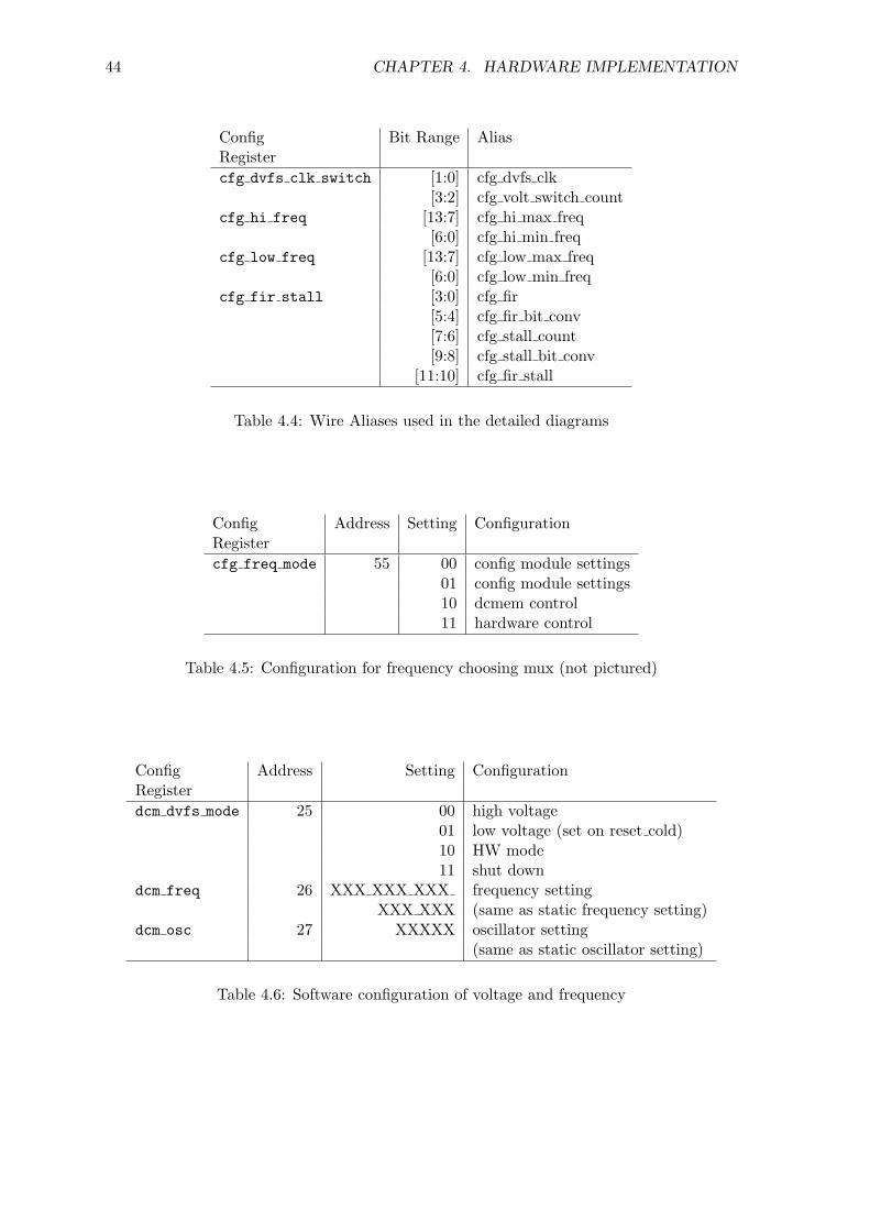
[5:4] cfg fir bit conv[7:6] cfg stall count[9:8] cfg stall bit conv
[11:10] cfg fir stall
Table 4.4: Wire Aliases used in the detailed diagrams
Config Address Setting ConfigurationRegistercfg freq mode 55 00 config module settings
01 config module settings10 dcmem control11 hardware control
Table 4.5: Configuration for frequency choosing mux (not pictured)
Config Address Setting ConfigurationRegisterdcm dvfs mode 25 00 high voltage
01 low voltage (set on reset cold)10 HW mode11 shut down
dcm freq 26 XXX XXX XXX frequency settingXXX XXX (same as static frequency setting)
dcm osc 27 XXXXX oscillator setting(same as static oscillator setting)
Table 4.6: Software configuration of voltage and frequency
4.3. FINAL CHIP IMPLEMENTATION DETAILS AND RESULTS 45
4.3 Final Chip Implementation Details and Results
The entire DVFS circuit including power gates, extra decoupling capacitors, supply
switch circuit, and DVFS controller was implemented on each individual AsAP processor
core in the AsAP multiprocessor architecture. The entire design was realized in 65 nm
technology. The DVFS components were designed as a wrapper to the AsAP processor
core, as shown in Figure 4.13.
Along the sides of the AsAP processor, there are a total of twenty four power
gates and four decoupling capacitors connected to the variable local power grid. The power
gate design is shown in Figure 4.14, which is designed with the blueprint in Figure 2.2, and
replicated twice vertically.
A performance loss analysis described in Figure 2.3 was performed on the scaled
current waveform of the AsAP processor core. Figure 4.15 displays the performance loss
and the associated power gate width. The twenty three power gates contain a total of
48x32 µm = 1536 µm of width on each voltage supply, which results in a performance loss
of an average of 2.5% for a single AsAP processor core.
The supply switch and DVFS controller logic were designed on a separate always-
on power supply. Additional features were added to the supply switch logic: an option to
disable the stall logic, and a backup mode to override the logic inputs to the power gates.
The variable buffer chain divides the power gates into four smaller submodules, where each
submodule contains an intermediate variable buffer chain controlling six power gates. The
variable delay mechanism can delay up to 32 ns, which can start at various stages during the
shut off of power. The DVFS controller reads in a two bit FIFO utilization signal from the
input FIFOs of the AsAP processor core. The stall period is also evaluated and processed.
The configuration of the AsAP oscillator is mapped to a register that can be incremented
and decremented.
The total area of the DVFS wrapper design occupies approximately 10,500 µm2,
which is 11.5% of an AsAP processor core area. The area composition is displayed in
Figure 4.16. The maximum power consumption of the DVFS circuit at 500 MHz is 1.38 mW,
which is 3.3% of the typical power of an AsAP processor (operating at 1.3V and 25oC).
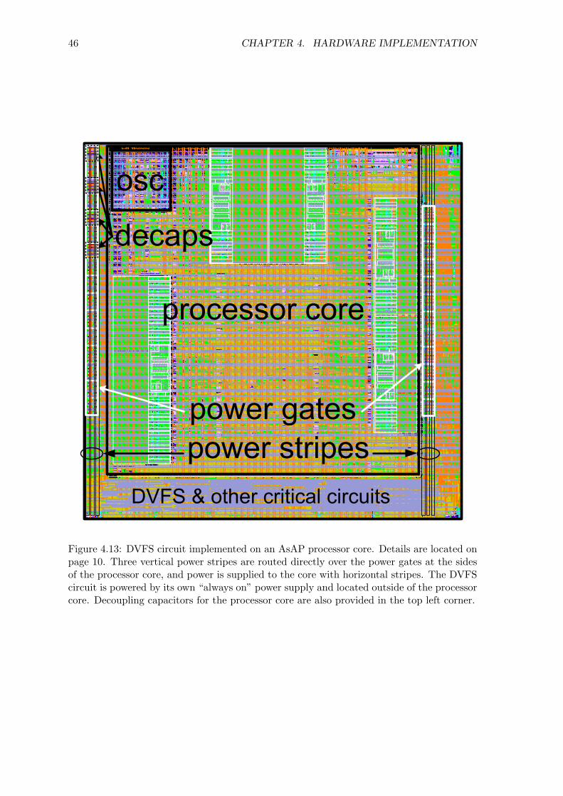
46 CHAPTER 4. HARDWARE IMPLEMENTATION
Figure 4.13: DVFS circuit implemented on an AsAP processor core. Details are located onpage 10. Three vertical power stripes are routed directly over the power gates at the sidesof the processor core, and power is supplied to the core with horizontal stripes. The DVFScircuit is powered by its own “always on” power supply and located outside of the processorcore. Decoupling capacitors for the processor core are also provided in the top left corner.
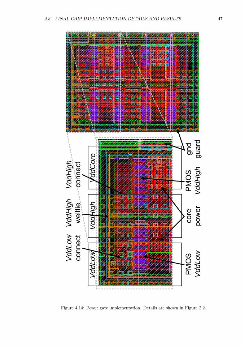
4.3. FINAL CHIP IMPLEMENTATION DETAILS AND RESULTS 47
Vdd
Low
Vdd
Hig
hV
ddC
ore
Vdd
Low
Vdd
Hig
h
Vdd
Hig
h
Vdd
Low
Vdd
Hig
h
Figure 4.14: Power gate implementation. Details are shown in Figure 2.2.
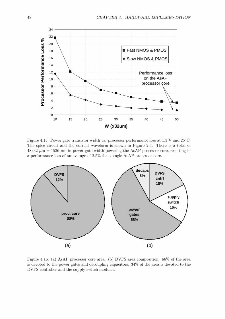
48 CHAPTER 4. HARDWARE IMPLEMENTATION
0
2
4
6
8
10
12
14
16
18
20
22
24
10 15 20 25 30 35 40 45 50
W (x32um)
Proc
esso
r Pe
rfor
man
ce L
oss
%
Fast NMOS & PMOS
Slow NMOS & PMOS
Performance loss on the AsAP
processor core
Figure 4.15: Power gate transistor width vs. processor performance loss at 1.3 V and 25oC.The spice circuit and the current waveform is shown in Figure 2.3. There is a total of48x32 µm = 1536 µm in power gate width powering the AsAP processor core, resulting ina performance loss of an average of 2.5% for a single AsAP processor core.
DVFS12%
proc. core88%
power gates58%
decaps8% DVFS
cntrl18%
supply switch16%
(a) (b)
Figure 4.16: (a) AsAP processor core area. (b) DVFS area composition. 66% of the areais devoted to the power gates and decoupling capacitors. 34% of the area is devoted to theDVFS controller and the supply switch modules.
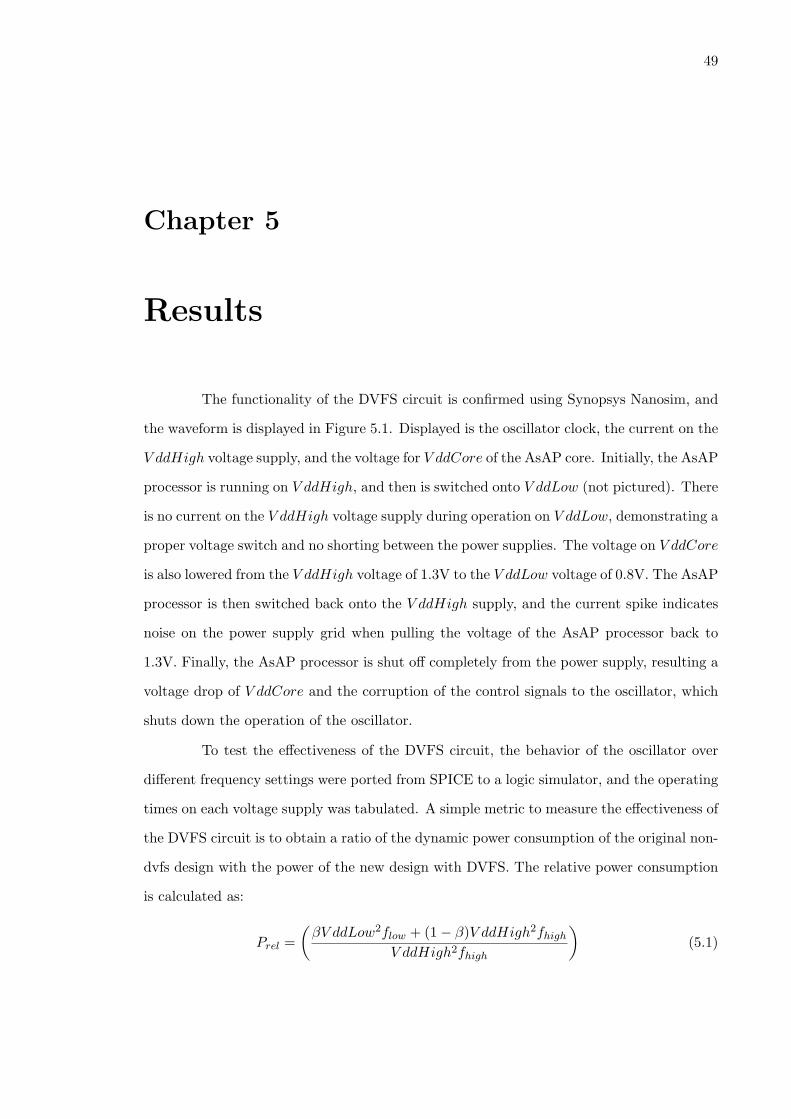
49
Chapter 5
Results
The functionality of the DVFS circuit is confirmed using Synopsys Nanosim, and
the waveform is displayed in Figure 5.1. Displayed is the oscillator clock, the current on the
V ddHigh voltage supply, and the voltage for V ddCore of the AsAP core. Initially, the AsAP
processor is running on V ddHigh, and then is switched onto V ddLow (not pictured). There
is no current on the V ddHigh voltage supply during operation on V ddLow, demonstrating a
proper voltage switch and no shorting between the power supplies. The voltage on V ddCore
is also lowered from the V ddHigh voltage of 1.3V to the V ddLow voltage of 0.8V. The AsAP
processor is then switched back onto the V ddHigh supply, and the current spike indicates
noise on the power supply grid when pulling the voltage of the AsAP processor back to
1.3V. Finally, the AsAP processor is shut off completely from the power supply, resulting a
voltage drop of V ddCore and the corruption of the control signals to the oscillator, which
shuts down the operation of the oscillator.
To test the effectiveness of the DVFS circuit, the behavior of the oscillator over
different frequency settings were ported from SPICE to a logic simulator, and the operating
times on each voltage supply was tabulated. A simple metric to measure the effectiveness of
the DVFS circuit is to obtain a ratio of the dynamic power consumption of the original non-
dvfs design with the power of the new design with DVFS. The relative power consumption
is calculated as:
Prel =(
βV ddLow2flow + (1− β)V ddHigh2fhigh
V ddHigh2fhigh
)(5.1)
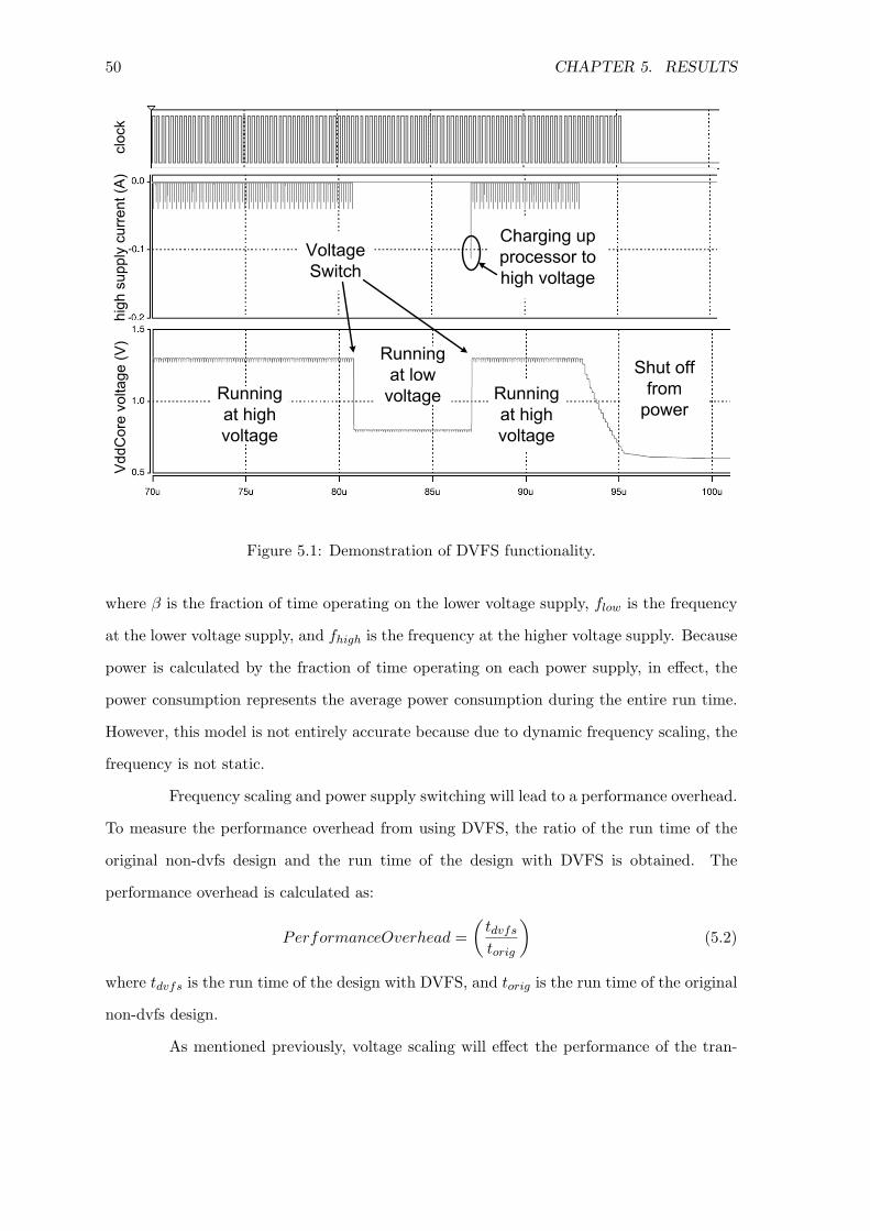
50 CHAPTER 5. RESULTS
Figure 5.1: Demonstration of DVFS functionality.
where β is the fraction of time operating on the lower voltage supply, flow is the frequency
at the lower voltage supply, and fhigh is the frequency at the higher voltage supply. Because
power is calculated by the fraction of time operating on each power supply, in effect, the
power consumption represents the average power consumption during the entire run time.
However, this model is not entirely accurate because due to dynamic frequency scaling, the
frequency is not static.
Frequency scaling and power supply switching will lead to a performance overhead.
To measure the performance overhead from using DVFS, the ratio of the run time of the
original non-dvfs design and the run time of the design with DVFS is obtained. The
performance overhead is calculated as:
PerformanceOverhead =(
tdvfs
torig
)(5.2)
where tdvfs is the run time of the design with DVFS, and torig is the run time of the original
non-dvfs design.
As mentioned previously, voltage scaling will effect the performance of the tran-
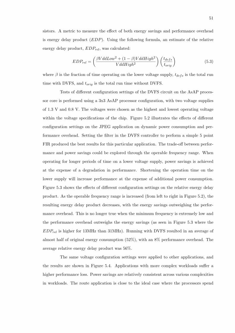
51
sistors. A metric to measure the effect of both energy savings and performance overhead
is energy delay product (EDP ). Using the following formula, an estimate of the relative
energy delay product, EDPrel, was calculated:
EDPrel =(
βV ddLow2 + (1− β)V ddHigh2
V ddHigh2
) (tdvfs
torig
)(5.3)
where β is the fraction of time operating on the lower voltage supply, tdvfs is the total run
time with DVFS, and torig is the total run time without DVFS.
Tests of different configuration settings of the DVFS circuit on the AsAP proces-
sor core is performed using a 3x3 AsAP processor configuration, with two voltage supplies
of 1.3 V and 0.8 V. The voltages were chosen as the highest and lowest operating voltage
within the voltage specifications of the chip. Figure 5.2 illustrates the effects of different
configuration settings on the JPEG application on dynamic power consumption and per-
formance overhead. Setting the filter in the DVFS controller to perform a simple 5 point
FIR produced the best results for this particular application. The trade-off between perfor-
mance and power savings could be explored through the operable frequency range. When
operating for longer periods of time on a lower voltage supply, power savings is achieved
at the expense of a degradation in performance. Shortening the operation time on the
lower supply will increase performance at the expense of additional power consumption.
Figure 5.3 shows the effects of different configuration settings on the relative energy delay
product. As the operable frequency range is increased (from left to right in Figure 5.2), the
resulting energy delay product decreases, with the energy savings outweighing the perfor-
mance overhead. This is no longer true when the minimum frequency is extremely low and
the performance overhead outweighs the energy savings (as seen in Figure 5.3 where the
EDPrel is higher for 13MHz than 31MHz). Running with DVFS resulted in an average of
almost half of original energy consumption (52%), with an 8% performance overhead. The
average relative energy delay product was 56%.
The same voltage configuration settings were applied to other applications, and
the results are shown in Figure 5.4. Applications with more complex workloads suffer a
higher performance loss. Power savings are relatively consistent across various complexities
in workloads. The route application is close to the ideal case where the processors spend
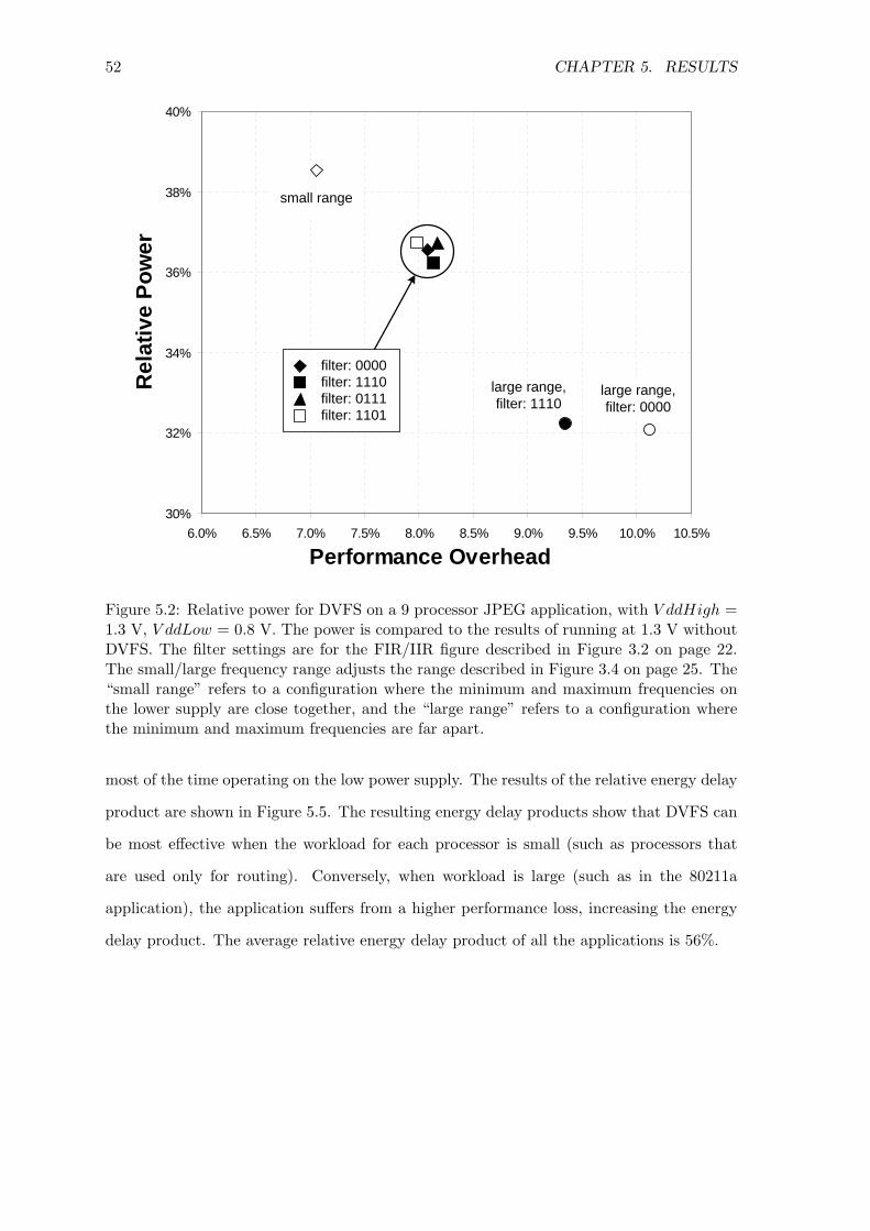
52 CHAPTER 5. RESULTS
30%
32%
34%
36%
38%
40%
6.0% 6.5% 7.0% 7.5% 8.0% 8.5% 9.0% 9.5% 10.0% 10.5%
Performance Overhead
Rel
ativ
e Po
wer
filter: 0000filter: 1110filter: 0111filter: 1101
small range
large range, filter: 0000
large range, filter: 1110
Figure 5.2: Relative power for DVFS on a 9 processor JPEG application, with V ddHigh =1.3 V, V ddLow = 0.8 V. The power is compared to the results of running at 1.3 V withoutDVFS. The filter settings are for the FIR/IIR figure described in Figure 3.2 on page 22.The small/large frequency range adjusts the range described in Figure 3.4 on page 25. The“small range” refers to a configuration where the minimum and maximum frequencies onthe lower supply are close together, and the “large range” refers to a configuration wherethe minimum and maximum frequencies are far apart.
most of the time operating on the low power supply. The results of the relative energy delay
product are shown in Figure 5.5. The resulting energy delay products show that DVFS can
be most effective when the workload for each processor is small (such as processors that
are used only for routing). Conversely, when workload is large (such as in the 80211a
application), the application suffers from a higher performance loss, increasing the energy
delay product. The average relative energy delay product of all the applications is 56%.
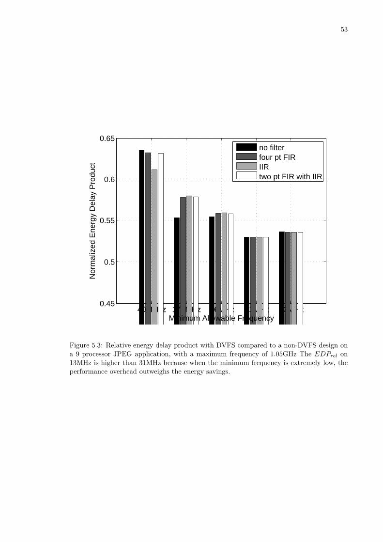
53
406MHz 174MHz 76MHz 31MHz 13MHz0.45
0.5
0.55
0.6
0.65
Minimum Allowable Frequency
Nor
mal
ized
Ene
rgy
Del
ay P
rodu
ct
no filterfour pt FIRIIRtwo pt FIR with IIR
Figure 5.3: Relative energy delay product with DVFS compared to a non-DVFS design ona 9 processor JPEG application, with a maximum frequency of 1.05GHz The EDPrel on13MHz is higher than 31MHz because when the minimum frequency is extremely low, theperformance overhead outweighs the energy savings.
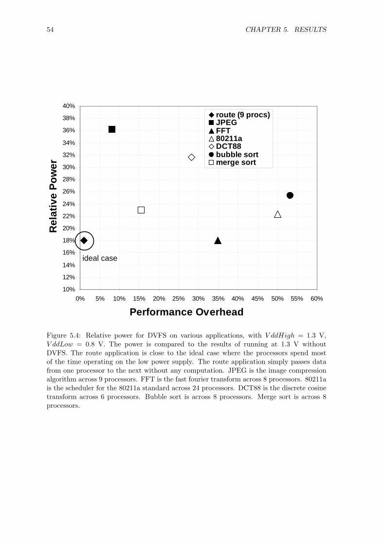
54 CHAPTER 5. RESULTS
10%
12%
14%
16%
18%
20%
22%
24%
26%
28%
30%
32%
34%
36%
38%
40%
0% 5% 10% 15% 20% 25% 30% 35% 40% 45% 50% 55% 60%
Performance Overhead
Rel
ativ
e Po
wer
route (9 procs)JPEGFFT80211aDCT88bubble sortmerge sort
ideal case
Figure 5.4: Relative power for DVFS on various applications, with V ddHigh = 1.3 V,V ddLow = 0.8 V. The power is compared to the results of running at 1.3 V withoutDVFS. The route application is close to the ideal case where the processors spend mostof the time operating on the low power supply. The route application simply passes datafrom one processor to the next without any computation. JPEG is the image compressionalgorithm across 9 processors. FFT is the fast fourier transform across 8 processors. 80211ais the scheduler for the 80211a standard across 24 processors. DCT88 is the discrete cosinetransform across 6 processors. Bubble sort is across 8 processors. Merge sort is across 8processors.
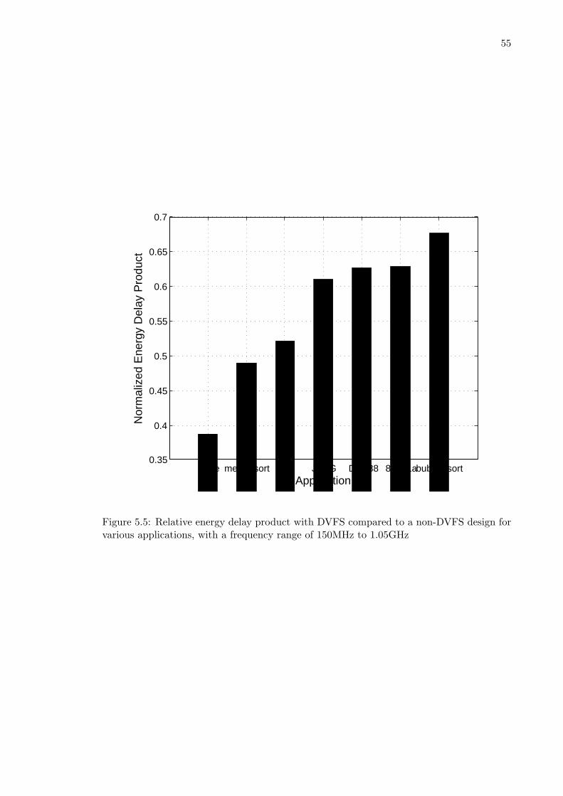
55
route merge sort FFT JPEG DCT88 80211abubble sort0.35
0.4
0.45
0.5
0.55
0.6
0.65
0.7
Application
Nor
mal
ized
Ene
rgy
Del
ay P
rodu
ct
Figure 5.5: Relative energy delay product with DVFS compared to a non-DVFS design forvarious applications, with a frequency range of 150MHz to 1.05GHz
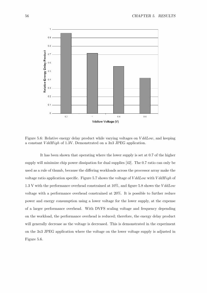
56 CHAPTER 5. RESULTS
Figure 5.6: Relative energy delay product while varying voltages on V ddLow, and keepinga constant V ddHigh of 1.3V. Demonstrated on a 3x3 JPEG application.
It has been shown that operating where the lower supply is set at 0.7 of the higher
supply will minimize chip power dissipation for dual supplies [42]. The 0.7 ratio can only be
used as a rule of thumb, because the differing workloads across the processor array make the
voltage ratio application specific. Figure 5.7 shows the voltage of V ddLow with V ddHigh of
1.3 V with the performance overhead constrained at 10%, and figure 5.8 shows the V ddLow
voltage with a performance overhead constrained at 20%. It is possible to further reduce
power and energy consumption using a lower voltage for the lower supply, at the expense
of a larger performance overhead. With DVFS scaling voltage and frequency depending
on the workload, the performance overhead is reduced; therefore, the energy delay product
will generally decrease as the voltage is decreased. This is demonstrated in the experiment
on the 3x3 JPEG application where the voltage on the lower voltage supply is adjusted in
Figure 5.6.
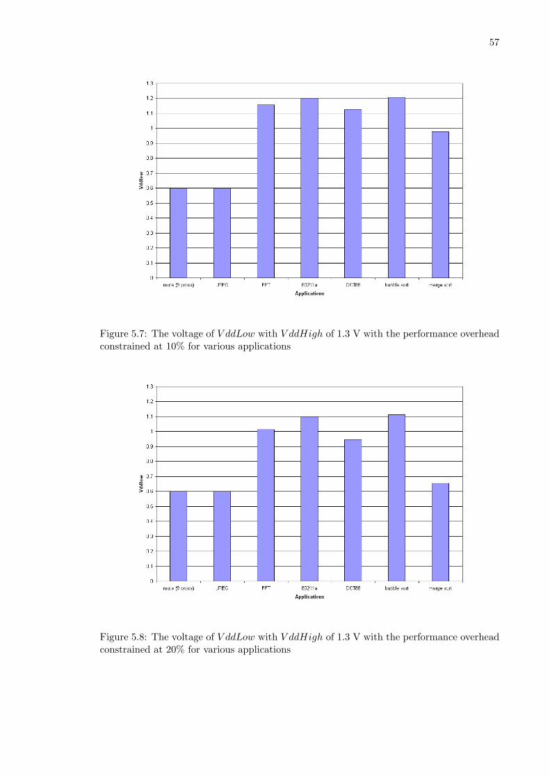
57
Figure 5.7: The voltage of V ddLow with V ddHigh of 1.3 V with the performance overheadconstrained at 10% for various applications
Figure 5.8: The voltage of V ddLow with V ddHigh of 1.3 V with the performance overheadconstrained at 20% for various applications
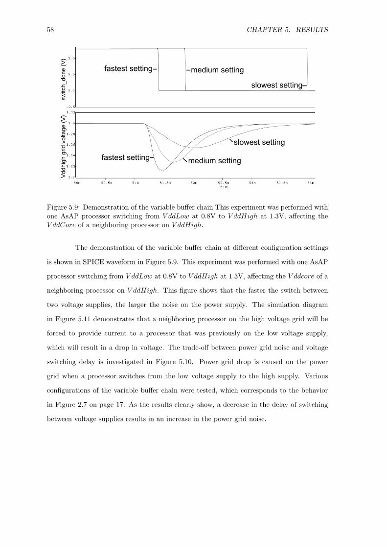
58 CHAPTER 5. RESULTS
Vdd
high
grid
vol
tage
(V)
switc
h_do
ne (V
)
Figure 5.9: Demonstration of the variable buffer chain This experiment was performed withone AsAP processor switching from V ddLow at 0.8V to V ddHigh at 1.3V, affecting theV ddCore of a neighboring processor on V ddHigh.
The demonstration of the variable buffer chain at different configuration settings
is shown in SPICE waveform in Figure 5.9. This experiment was performed with one AsAP
processor switching from V ddLow at 0.8V to V ddHigh at 1.3V, affecting the V ddcore of a
neighboring processor on V ddHigh. This figure shows that the faster the switch between
two voltage supplies, the larger the noise on the power supply. The simulation diagram
in Figure 5.11 demonstrates that a neighboring processor on the high voltage grid will be
forced to provide current to a processor that was previously on the low voltage supply,
which will result in a drop in voltage. The trade-off between power grid noise and voltage
switching delay is investigated in Figure 5.10. Power grid drop is caused on the power
grid when a processor switches from the low voltage supply to the high supply. Various
configurations of the variable buffer chain were tested, which corresponds to the behavior
in Figure 2.7 on page 17. As the results clearly show, a decrease in the delay of switching
between voltage supplies results in an increase in the power grid noise.
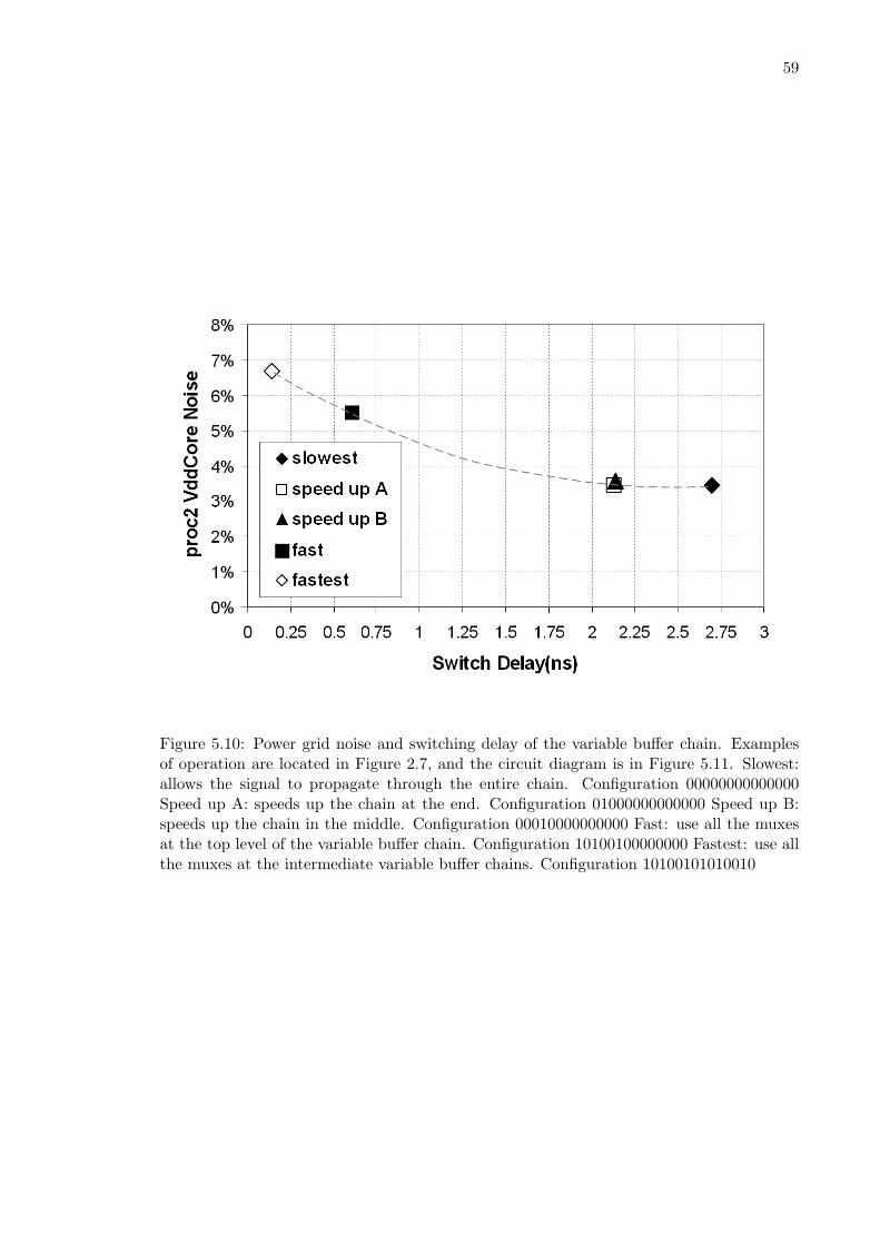
59
Figure 5.10: Power grid noise and switching delay of the variable buffer chain. Examplesof operation are located in Figure 2.7, and the circuit diagram is in Figure 5.11. Slowest:allows the signal to propagate through the entire chain. Configuration 00000000000000Speed up A: speeds up the chain at the end. Configuration 01000000000000 Speed up B:speeds up the chain in the middle. Configuration 00010000000000 Fast: use all the muxesat the top level of the variable buffer chain. Configuration 10100100000000 Fastest: use allthe muxes at the intermediate variable buffer chains. Configuration 10100101010010
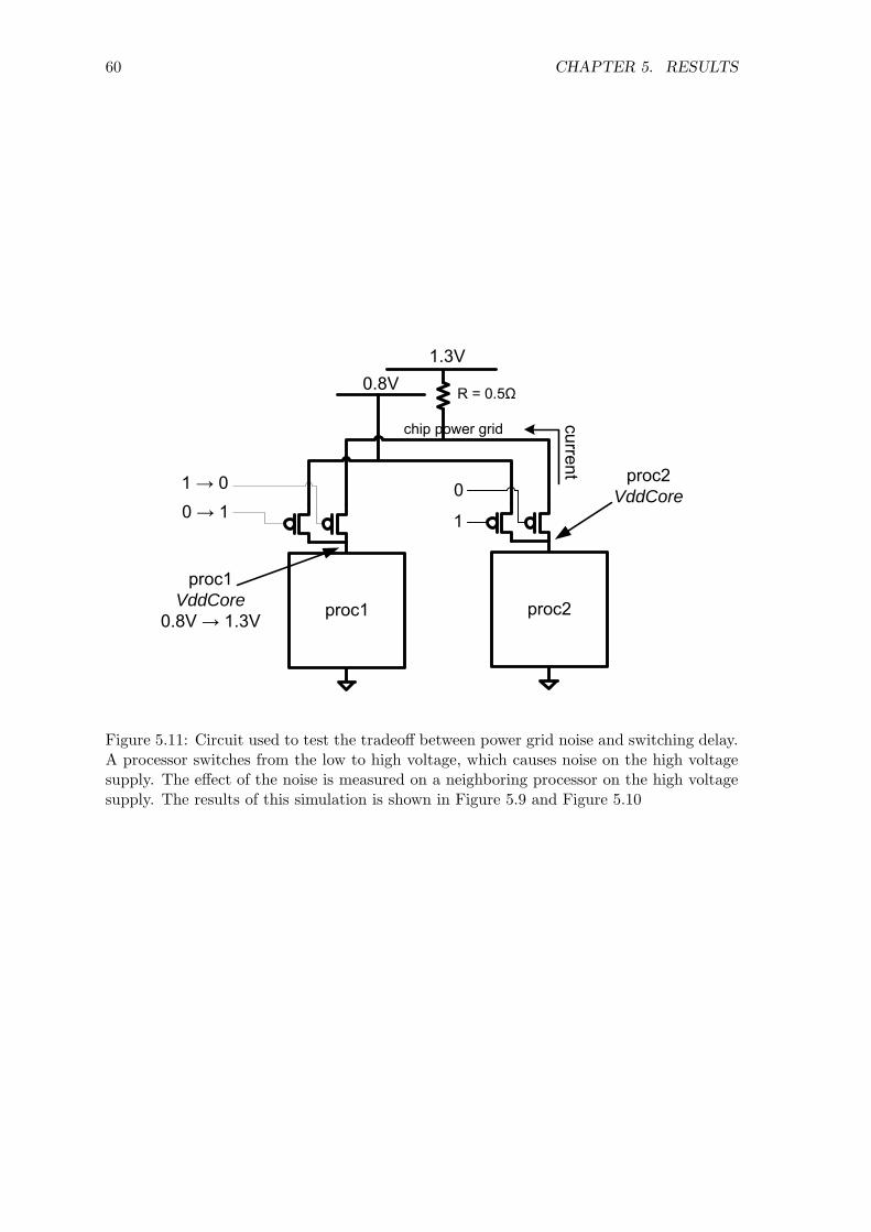
60 CHAPTER 5. RESULTS
0.8V
0 → 11 → 0
proc1
1
0
proc2
1.3V
chip power grid current proc2 VddCore
proc1 VddCore
0.8V → 1.3V
R = 0.5Ω
Figure 5.11: Circuit used to test the tradeoff between power grid noise and switching delay.A processor switches from the low to high voltage, which causes noise on the high voltagesupply. The effect of the noise is measured on a neighboring processor on the high voltagesupply. The results of this simulation is shown in Figure 5.9 and Figure 5.10
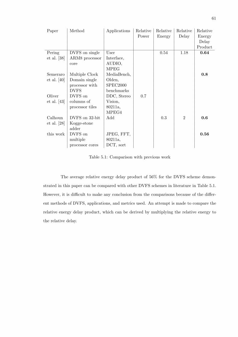
61
Paper Method Applications Relative Relative Relative RelativePower Energy Delay Energy
DelayProduct
Pering DVFS on single User 0.54 1.18 0.64et al. [38] ARM8 processor Interface,
core AUDIO,MPEG
Semeraro Multiple Clock MediaBench, 0.8et al. [40] Domain single Olden,
processor with SPEC2000DVFS benchmarks
Oliver DVFS on DDC, Stereo 0.7et al. [43] columns of Vision,
processor tiles 80211a,MPEG4
Calhoun DVFS on 32-bit Add 0.3 2 0.6et al. [28] Kogge-stone
adderthis work DVFS on JPEG, FFT, 0.56
multiple 80211a,processor cores DCT, sort
Table 5.1: Comparison with previous work
The average relative energy delay product of 56% for the DVFS scheme demon-
strated in this paper can be compared with other DVFS schemes in literature in Table 5.1.
However, it is difficult to make any conclusion from the comparisons because of the differ-
ent methods of DVFS, applications, and metrics used. An attempt is made to compare the
relative energy delay product, which can be derived by multiplying the relative energy to
the relative delay.
62
Chapter 6
Conclusion
Dynamic voltage and frequency scaling logic on a multiple voltage domain architec-
ture provides significant power savings with little performance and area overhead. Voltage
scaling is performed across two voltage supplies using PMOS power gates. The workload for
each logic core is filtered and transformed to scale the frequency and voltage dynamically.
A highly configurable interface supports optimal settings for various workload behaviors.
The techniques of voltage scaling discussed in this paper are applicable to both current and
future architectures and silicon technologies.
In addition to the topics covered in this paper, there are numerous avenues left to
be explored:
1. A global chip controller can be devised, so that the outside voltage supply can scale
depending on the states of the logic cores within the chip.
2. NMOS power gates with multiple grounds remains a possibility depending on the chip
technology.
3. Dynamic configuration of the DVFS logic can produce more optimal power savings
and performance.
63
Bibliography
[1] International technology roadmap for semicondutors. Inhttp://www.itrs.net/reports.html, 2006.
[2] S. Borkar. Low power design challenges for the decade. 2001.
[3] J. Rabaey, A. Chandrakasan, and B. Nikolic. In Digital Integrated Circuits 2nd Edition,2002.
[4] S. Kang and Y. Leblebici. CMOS digital integrated circuits analysis and design. 2003.
[5] K. Usami and M. Horowitz. Clustered voltage scaling technique for low-power design.In International Symposium on Low Power Electronics and Design, 1995.
[6] M. Igarashi, K. Usami, K. Nogami, F. Minami, Y. Kawasaki, T. Aoki, M. Takano,C. Mizuno, T. Ishikawa, M. Kanazawa, S. Sonoda, M. Ichida, and N. Hatanaka. Alow-power design method using multiple supply voltages. In International Symposiumon Low Power Electronics and Design, pp. 36-41, 1997.
[7] Z. Hu, A. Buyuktosunoglu, V. Srinivasan, V. Zyuban, H. Jacobson, and P. Bose.Microarchitectural techniques for power gating of execution units. In InternationalSymposium on Low Power Electronics and Design, 2004.
[8] C. Long and L. He. Distributed sleep transistor network for power reduction. In IEEETransactions on Very Large Scale Integration Systems, Vol. 32, No. 9, 2004.
[9] K. Usami and N. Ohkubo. A design approach for fine-grained run-time power gatingusing locally extracted sleep signals. In International Conference on Computer Design,2006.
[10] K. Agarwal and K. Nowka. Dynamic power management by combination of dualstatic supply voltages. In Proceedings of the 8th International Symposium on QualityElectronic Design, 2007.
[11] B. Baas. A parallel programmable energy-efficient architecture for computationally-intensive DSP systems. In Signals, Systems and Computers, 2003. Conference Recordof the Thirty-Seventh Asilomar Conference on, November 2003.
[12] S. Borkar, T. Karnik, and V. De. Design and reliability challenges in nanometertechnologies. In 41st Design Automation Conference pp. 75-75, 2004.
[13] K. Bowman, S. Duvall, and J. Meindl. Impact of die-to-die and within-die parameterfluctuations on the maximum clock frequency distribution for gigascale integration. InIEEE Journal of Solid-State Circuits, Vol. 37, No. 2, February 2002.
64 BIBLIOGRAPHY
[14] S. Borkar, T. Karnik, S. Narendra, J. Tschanz, A. Keshavarzi, and V. De. Parametervariations and impacts on circuits and microarchitecture. In 40th Design AutomationConference p. 338, 2003.
[15] Y. Liu, H. Yang, R. Dick, H. Wang, and L. Shang. Thermal vs energy optimization fordvfs-enabled processors in embedded systems. In Proceedings of hte 8th InternationalSymposium on Quality Electronic Design, 2007.
[16] Z. Yu, M. Meeuwsen, R. Apperson, O. Sattari, M. Lai, J. Webb, E. Work, T. Mohsenin,M. Singh, and B. Baas. An asynchronous array of simple processors for DSP applica-tions. In IEEE International Solid-State Circuits Conference, (ISSCC ’06), February2006.
[17] D. M. Chapiro. Globally-asynchronous locally-synchronous systems. In PhD thesis,Stanford University, Stanford, CA, October 1984.
[18] M. Nakai, S. Akui, K. Seno, T. Meguro, T. Seki, T. Kondo, A. Hashiguchi, H. Kawa-hara, K. Kumano, and M. Shimura. Dynamic voltage and frequency management fora low-power embedded microprocessor. In IEEE Journal of Solid-State Circuits, Vol.40, No. 1, January 2005.
[19] V. Gutnik and A. Chandrakasan. Embedded power supply for low-power dsp. In IEEETransactions on VLSI Systems, Vol. 5, No. 4, December 1997.
[20] T. Burd, T. Pering, A. Stratakos, and R. Brodersen. A dynamic voltage scaled micro-processor system. In IEEE Journal of Solid-State Circuits, Vol. 35, No. 11, November2000.
[21] K. Nowka, G. Carpenter, E. MacDonald, H. Ngo, B. Brock, K. Ishii, T. Nguyen, andJ. Burns. A 32-bit powerpc system-on-a-chip with support for dynamic voltage scalingand dynamic frequency scaling. In IEEE Journal of Solid-State Circuits, Vol. 37, No.11, November 2002.
[22] L. Clark, E. Hoffman, J. Miller, M. Biyani, Y. Liao, S. Strazdus, M. Morrow, K. Ve-larde, and M. Yarch. An embedded 32-b microprocessor core for low-power and high-performance applications. In IEEE Journal of Solid-State Circuits, Vol. 36 No. 11,November 2001.
[23] A. Stratakos, S. Sanders, and R. Brodersen. A low-voltage cmos dc-dc converter for aportable battery-operated system. 1994.
[24] S. Musunuri, P.L. Chapman, J. Zou, and C. Liu. Inductor design for monolithic dc-dcconverters. In IEEE 34th Annual Power Electronics Specialist Conference, 2003.
[25] L. Milner and G. Rincon-Mora. A novel predictive inductor multiplier for integratedcircuit dc-dc converters in portable applications. In International Symposium on LowPower Electronics and Design, 2005.
[26] Y. Ye, S. Borkar, and V. De. A new technique for standby leakage reduction in high-performance circuits. In Symposium on VLSI Circuits Digest of Technical Papers,1998.
BIBLIOGRAPHY 65
[27] F. Dabiri, R. Jafari, A. Nahapetian, and M. Sarrafzadeh. A unified optimal voltageselection methodology for low-power systems. In Proceedings of the 8th InternationalSymposium on Quality Electronic Design, 2007.
[28] B. Calhoun and A. Chandrakasan. Ultra-dynamic voltage scaling (udvs) using sub-threshold operation and local voltage dithering. In IEEE Journal of Solid-State Cir-cuits, Vol. 41, No. 1, January 2006.
[29] A. Gayasen, K. Lee, N. Vijaykrishnan, M. Kandemir, M.J. Irwin, and T. Tuan. Adual-vdd low power fpga architecture. In Field Programmable Logic and Application,Lecture Notes in Computer Science pp. 145-157, 2004.
[30] S. Martin, K. Flautner, T. Mudge, and D. Blaauw. Combined dynamic voltage scalingand adaptive body biasing for lower power microprocessors under dynamic workloads.In International Conference on Computer-Aided Design, pp. 721-725, 2002.
[31] B. Choi and Y. Shin. Lookup table-based adaptive body biasing of multiple macros.In 8th International Symposium on Quality Electronic Design, 2007.
[32] J. Tschanz, S. Narendra, Y. Ye, B. Bloechel, S. Borkar, and V. De. Dynamic sleeptransistor and body bias for active leakage power control of microprocessors. In IEEEJournal of Solid-State Circuits, Vol. 38, No. 11, November 2003.
[33] M.J. Hargrove, S. Voldman, R. Gauthier, J. Brown, K. Duncan, and W. Craig. Latchupin cmos technology. In 36th Annual International Reliability Physics Symposium, 1998.
[34] K. Shepard and V. Narayanan. Noise in deep submicron digital design. In InternationalSymposium on Low Power Electronics and Design, p. 524, 1996.
[35] H. Jiang, M. Marek-Sadowska, and S. Nassif. Benefits and costs of power-gating tech-nique. In Proceedings of the 2005 International Conference on Computer Design, 2005.
[36] M. Anis, S. Areibi, M. Mahmoud, and M. Elmasry. Dynamic and leakage powerreduction in mtcmos circuits using an automated efficient gate clustering technique. In39th Design Automation Conference, p. 480, 2002.
[37] Y. Kanno, H. Mizuno, Y. Yasu, K. Hirose, Y. Shimazaki, T. Hoshi, Y. Miyairi, T. Ishii,T. Yamada, T. Irita, T. Hattori, K. Yanagaisawa, and N. Irie. Hierarchical powerdistribution with power tree in dozens of power domains for 90-nm low-power multi-cpu socs. In IEEE Journal of Solid-State Circuits, Vol. 42, No. 1, January 2007.
[38] T. Pering, T. Burd, and R. Brodersen. The simulation and evaluation of dynamicvoltage scaling algorithms. In ISLPED, August 1998.
[39] K. Govil, E. Chan, and H. Wasserman. Comparing algorithms for dynamic speed-setting of a low-power cpu. In MOBICOM, 1995.
[40] G. Semeraro, G. Magklis, R. Balasubramonian, D. Albonesi, S. Dwarkadas, andM. Scott. Energy-efficient processor design using multiple clock domains with dynamicvoltage and frequency scaling. In Proceedings of the Eighth International Symposiumon High-Performance Computer Architecture, 2002.
66 BIBLIOGRAPHY
[41] P. Pillai and K. Shin. Real-time dynamic voltage scaling for low-power embeddedoperating systems. In ACM Symposium on Operating Systems Principles, pp. 89 -102, 2001.
[42] T. Kuroda and M. Hamada. Low-power cmos digital design with dual embeddedadaptive power supplies. In IEEE Journal of Solid-State Circuits, Vol. 35, No. 4,April 2000.
[43] J. Oliver, R. Rao, P. Sultana, J. Crandall, E. Czernikowski, L. Jones, D. Franklin,V. Akella, and F. Chong. Synchroscalar: A multiple clock domain, power-aware, tile-based embedded processor. In Proceedings of the 31st Annual International Symposiumon Computer Architecture, 2004.
[44] J. Kao, S. Narendra, and A. Chandrakasan. Mtcmos hierarchical sizing based on mutualexclusive discharge patterns. In 35th Conference on Design Automation Conference ,pp. 495-500, 1998.
[45] H. Chen and D. Ling. Power supply noise analysis methodology for deep-submicronvlsi chip design. In 34th Conference on Design Automation Conference, p. 638, 1997.