april 20, 2009 super-integration. 2 about sixis founded may 2008 spun out of rti international $5m...
TRANSCRIPT

April 20, 2009
Super-Integration

2
About siXis
•Founded May 2008• Spun out of RTI International• $5M Series A funding in June 2008• Investors: Intersouth Partners, RTI International• CED “Spin-out of the Year Award”
•Major technology focus on silicon circuit board technology• Initial application in high performance reconfigurable computing
•Headquartered in Research Triangle Park, NC• Veteran senior management team in place• Co-located with semiconductor fab facility

www.rti.org
RTI International at a Glance
• Established in 1958• 2600 employees
– half with advanced degrees• Revenue of $0.6B• Multidisciplinary research institute:
technology, health solutions, statistical and social sciences
RTI is the second largest private
nonprofit R&D organization in USA.
RTI interest in 3D integration: • 3D integration technology
development since 2000 (MCNC)• Spin-off in bonding technology:
Ziptronix
180-Acre Campus
810,000 sq. ft Space
24 Buildings
siXis Technology Overview

Key Value Proposition
• Maximize Performance per cm2-W with Super-Integration• Go beyond stepper reticle limits• Integrate different technologies, e.g.
• DRAM• Logic – FPGA, processor• Analog – ADC, DAC, RF• Passives – resistors, capacitors
• Fit into existing infrastructure• Sustaining technology
5
Single Die
Super-Integration
Die Size
Co
st
reticle limits
5

Super-Integration Top View
6
FPGADie
MEM1Gb
MEM1Gb
MEM1Gb
MEM1Gb
MEM1Gb
MEM1Gb
MEM1Gb
MEM1Gb
MEM1Gb
MEM1Gb
MEM1Gb
MEM1Gb
MEM1Gb
MEM1Gb
MEM1Gb
MEM1GbFPGA
Package
42.5mm x 42.5mm
MEMORY1Gb
MEMORY1Gb
MEMORY1Gb
MEMORY1Gb
MEMORY1Gb
MEMORY1Gb
MEMORY1Gb
MEMORY1Gb
MEMORY1Gb
MEMORY1Gb
MEMORY1Gb
MEMORY1Gb
MEMORY1Gb
MEMORY1Gb
MEMORY1Gb
MEMORY1Gb
5117 sq. mm
2045 sq. mm
Super-Integration
ConventionalSuper-
Integration ∆
Area (sq. mm) 5,117 2,045 -60%
Total Pads 3,072 1,760 -43%
Power Pads 1,312 1,312 -
I/O Pads 1,760 448 -75%
SiCBSilicon Circuit Board
FR-4PCB
Conventional
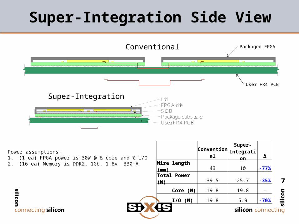
Super-Integration Side View
7
Conventional
Super-Integration
ConventionalSuper-
Integration ∆
Wire length (mm) 43 10 -77%
Total Power (W) 39.5 25.7 -35%
Core (W) 19.8 19.8 -
I/O (W) 19.8 5.9 -70%
LidFPGA dieSiCBPackage substrateUser FR4 PCB
Packaged FPGA
User FR4 PCB
7
Power assumptions:1. (1 ea) FPGA power is 30W @ ½ core and ½ I/O2. (16 ea) Memory is DDR2, 1Gb, 1.8v, 330mA

siXis Product Roadmap
8
· Single-board · 19" Rack mount 1U enclosure· 4 Compute nodes· 16 QSFP sockets· PPC Management Processor
De
ns
ity
(C
om
pu
te N
od
es
/ R
U)
· 3 boards· 19" Rack mount 4U enclosure· 4 Compute nodes· 10 CX4 sockets· MicroBlaze Management Processor
Time
· Single-board · 19" Rack mount 1U enclosure· 16 Compute nodes· 16 QSFP sockets· PPC Management Processor
1
4
16
ConventionalPackaging
ConventionalPackaging
Super-Integration SiCB

SX2000 (Conventional Packaging 1U Shelf)
9
FPGAFPGA FPGAFPGA
Flash
LVDS 12.8Gbps Full Duplex
LVDS 12.8Gbps Full Duplex
LVDS 12.8Gbps Full Duplex
MGT
RJ4
5/U
SB
Mic
roS
D A
da
pte
r
QS
FP
QS
FP
QS
FP
QS
FP
QS
FP
QS
FP
QS
FP
QS
FP
QS
FP
QS
FP
QS
FP
QS
FP
QS
FP
QS
FP
QS
FP
QS
FP
Memory4 ports/FPGA
4Gb (x16)
Front Panel
Power Supply
Compute Node
LVDS 12.8Gbps Full Duplex
Fla
shPPC Fla
sh
PPC Fla
shPPCFla
shPPC

10
FPGA Package
42.5mm x 42.5mm
MEMORY1Gb
MEMORY1Gb
MEMORY1Gb
MEMORY1Gb
MEMORY1Gb
MEMORY1Gb
MEMORY1Gb
MEMORY1Gb
MEMORY1Gb
MEMORY1Gb
MEMORY1Gb
MEMORY1Gb
MEMORY1Gb
MEMORY1Gb
MEMORY1Gb
MEMORY1Gb
PPC
ME
MO
RY
1Gb
ME
MO
RY
1Gb
ME
MO
RY
1Gb
ME
MO
RY
1Gb
1Gb
NA
ND
63 pin
s10.5x13
FPGADie
MEM1Gb
MEM1Gb
MEM1Gb
MEM1Gb
MEM1Gb
MEM1Gb
MEM1Gb
MEM1Gb
MEM1Gb
MEM1Gb
MEM1Gb
MEM1Gb
MEM1Gb
MEM1Gb
MEM1Gb
MEM1Gb
PPCdie
ME
M1G
bM
EM
1Gb
flashM
EM
1Gb
ME
M1G
b
50mm x 50mm = 2500 sq. mm
83mm x 92mm = 7636 sq. mm
Compute NodeConventional Compute Node
SiCB Compute Node

11
SX3000 (Super-Integration SiCB 1U Shelf)
Flash
MGT
RJ4
5/U
SB
Mic
ro S
D
QS
FP
QS
FP
QS
FP
QS
FP
QS
FP
QS
FP
QS
FP
QS
FP
QS
FP
QS
FP
QS
FP
QS
FP
QS
FP
QS
FP
QS
FP
QS
FP
Front Panel
Power Supply
Compute Node
Compute Node
Compute Node
Compute Node
Compute Node
Compute Node
Compute Node
Compute Node
Compute Node
Compute Node
Compute Node
Compute Node
Compute Node
Compute Node
Compute Node
Compute Node

siXis FPGA Programming Model
• RTL Programming Model• Verilog & VHDL – brute force, slow, wysiwyg
• C Models – faster, more hardware, silicon aware, scheduler• Impulse-C • Cebatech C2R
• Matlab to RTL --scheduler, more hardware• Xilinx Accelchip
• DSP to RTL• Simulink to FPGA • Synplify DSP -- Synopsys/Synplicity• DSP Builder – Altera• System Generator – Xilinx
12

siXis Product Roadmap
13
· Single-board · 19" Rack mount 1U enclosure· 4 Compute nodes· 16 QSFP sockets· PPC Management Processor
De
ns
ity
(C
om
pu
te N
od
es
/ R
U)
· 3 boards· 19" Rack mount 4U enclosure· 4 Compute nodes· 10 CX4 sockets· MicroBlaze Management Processor
Time
· Single-board · 19" Rack mount 1U enclosure· 16 Compute nodes· 16 QSFP sockets· PPC Management Processor
1
4
16
ConventionalPackaging
ConventionalPackaging
Super-Integration SiCB
End