arashanzalchi ieee transactions on ias - … (vsi), is designed and analyzed. in order to attenuate...
TRANSCRIPT

0093-9994 (c) 2016 IEEE. Personal use is permitted, but republication/redistribution requires IEEE permission. See http://www.ieee.org/publications_standards/publications/rights/index.html for more information.
This article has been accepted for publication in a future issue of this journal, but has not been fully edited. Content may change prior to final publication. Citation information: DOI 10.1109/TIA.2017.2712783, IEEETransactions on Industry Applications
IEEE TRANSACTIONS ON INDUSTRY APPLICATIONS 1
Design and Analysis of a Higher Order Power Filter for
Grid-Connected Renewable Energy SystemsArash Anzalchi, Student Member, IEEE, Masood Moghaddami, Student Member, IEEE,
Amir Moghadasi, Member, IEEE, Maneli Malek Pour, Student Member, IEEE and Arif Sarwat, Member, IEEE
Abstract—Harmonic compensation is regularly implementedfor a grid-tied inverter to reduce the influence of the grid currentand voltage harmonics. In this study, the L(LCL)2 filter, which isa high order power filter for single-phase grid-tied voltage-sourceinverters (VSI), is designed and analyzed. In order to attenuatethe high-frequency harmonics, additional resonant branch at thedouble of the switching frequency is added to the LLCL filter.The total inductance of this filter is almost less than the LLCL
filter with the amount of the grid side inductor. A comparativestudy on filter parameter design, size estimation, efficiency,stability, and dc-link dynamics in bi-directional power flowapplications between the LLCL filter and the proposed L(LCL)2filter have been conducted. The assessment of these studies arepresented through both experimental hardware implementationand Matlab/Simulink-based simulation on a 700 W, 120V / 60Hz single-phase grid-tied inverter. It is concluded that, comparedto the LLCL filter, the L(LCL)2 filter not only has less voltagedrop and total component size but also has better performanceon reducing high order current harmonics. Additionally, theL(LCL)2 filter has a smaller size, less losses, stable closed loopcontrol system, and compared to traditional LLCL filter, it doesnot add any control difficulty to the system.
Index Terms—current harmonics; LCL-filter; LLCL filter;L(LCL)2 filter; Power quality; switching-frequency; voltage-source inverter (VSI).
I. INTRODUCTION
RENEWABLE energy sources and distributed generation
(DG) resources are mostly connected to the power grid
through a grid-connected inverter [1]. In order to limit the
excessive current harmonics, which are mostly produced by
sine pulse width modulation (PWM), a low-pass power filter
is usually put in between a voltage-source inverter (VSI) and
the grid [2], [3]. The use of the PWM system necessitates
an output filter to limit the grid-injected current harmonics,
in order to satisfy the IEEE 1547.2-2008 and IEEE 519-
2014 standards. L-filters are typically used but they have the
drawbacks of slow dynamic response and big inductor value
[4], [5]. The first-order L filter can meet the standards for
the grid interconnection with notably smaller size and cost
compared to an LCL filter, primarily for applications in several
kilowatts [6]–[8].
For industrial uses, the cost of the components is a vital
aspect of selecting the power filter for the grid-tied inverter.
Owing to the growing cost of copper, various methods have
been implemented to cut down the price of the power filter.
One helpful way is to increase the switching frequency of
the inverter where the method, surely, depends on the device
proficiency and cost.
Nowadays, most power electronic designs are limited by
thermal constraints. Power dissipation and surface area have
a major influence on temperature increase. The volume and
size of the component are two measures that the surface area
of the object is directly linked with. The use the total power
loss of the LCL filter as the optimization factor in the design
was introduced in [9]. The objective of the algorithm was to
reduce the size, weight, and absolutely the cost of the LCL
filter.
Special topologies and control configurations are other
measures which have motivated scholars. [10] introduced a
three-level neutral point clamped (NPC) converter as a high
power renewable energy grid interface, trying to achieve higher
switching frequency and better efficiency. An LLCL topology
with two resonant circuits between the ripple inductor and the
grid-side inductor i to suppress the two dominant harmonic
currents around the switching frequency and the double of the
switching frequency.
The conducted Electromagnetic Interference (EMI) issues
for the high-order power-filter-based single-phase full-bridge
grid-tied inverter by means of the unipolar modulation in dis-
continuous mode was considered in [11]. In order to minimize
the additional reactive power as well as to achieve a small
value of the capacitor, a differential mode EMI suppressor
for the LLCL filter based system was proposed in [12]. To
decrease the overall inductance value, without increasing the
capacitive reactive power, the modified LCL filter topology by
using an extra parallel LC resonant circuit was suggested in
[13]. A capacitor-current-feedback active damping by means
of reduced computation delay was proposed in [14]. By using
this method, the virtual impedance functions more similar to a
resistor in a wider frequency range, and the unstable poles of
the open loop are eliminated; consequently, great robustness
against the grid impedance deviation is attained. The magnetic
integration of the LCL filter in grid-connected inverters was
investigated in [15]. By placing the windings accurately and
sharing an ungapped core, the major fluxes created by the two
inductors of an LCL filter cancel out mostly in the common
core.
This paper is an extension of our earlier publications [16],
[17] which proposed a modified high-order filter design,
named L(LCL)2 filter, based on the conventional LLCL filter.
This filter can reduce the harmonics at the switching frequency
and multiples of the switching frequency while saving the
total inductance and thereby results in size reduction of the
filter. The most important role of the grid side inductor in the
traditional LLCL filter is to decrease the harmonics around
the twice of the switching frequency. In the new topology, this

0093-9994 (c) 2016 IEEE. Personal use is permitted, but republication/redistribution requires IEEE permission. See http://www.ieee.org/publications_standards/publications/rights/index.html for more information.
This article has been accepted for publication in a future issue of this journal, but has not been fully edited. Content may change prior to final publication. Citation information: DOI 10.1109/TIA.2017.2712783, IEEETransactions on Industry Applications
IEEE TRANSACTIONS ON INDUSTRY APPLICATIONS 2
S2
S3
S4
L11 L21
vg
ii ig
LLCL Filter
PLL
S1
Vdc Cdc
STM32F4Discovery
Microcontroller
Lf
Cf
Iref
RL
ig
B
A
vi
if
Fig. 1. Schematic diagram of the LLCL filter.
S2
S3
S4
ii
L(LCL)2 Filter
S1
Vdc
Cdc=Ceq
STM32F4Discovery
Microcontroller
Lf1
Cf1
Lf2
Cf 2
L12 L22 L32
Cf1+ Cf2= Cf
L12+ L22+ L32= L11
vg
ig
PLL
Iref
RL
ig
vi
B
A
LDC-eq
Pext PDC
if1 if2
Fig. 2. Schematic of L(LCL)2 system.
inductor is removed, and the converter side inverter of the filter
is split into three parts. Then, two resonant traps at switching
frequency and double of switching frequency are inserted in
between the converter side inductor. The proposed filter is able
to attenuate the current ripple components better than the LCL
and traditional LLCL filters. This study can pave the path for
the design and implementation of the L(LCL)2 filter in VSI
applications. This work has also presented the tools for further
exploring the L(LCL)2 filters for other case studies, such as
analyzing the stability of the system, optimizing the filter
parameters, designing damping methods and EMI suppressor
for the filter, etc.
The outline of the rest of the paper is as follows. First,
the principle of an LLCL filter is presented for a single-phase
power converter. Next, the engineering design procedure of
the L(LCL)2 filter is proposed in Section II. Size estimation
and efficiency analysis are presented in part B and C of
Section II, respectively. In order to confirm the correctness
of theoretical analysis, comparison of the simulation and
experimental results for both LLCL and L(LCL)2 filters are
illustrated in Section II. Closed loop stability analysis of
the current controller and the small-signal model of dc-link
dynamics are studied in this section as well. Eventually, we
conclude the paper in Section IV.
II. PARAMETER DESIGN OF THE L(LCL)2 FILTER
The circuit configuration of an LLCL and L(LCL)2 filter-
based single phase grid-tied VSI is shown in Figs. 1 and 2
respectively. The inverter output voltage and current of the
LLCL filter are represented as vi (between points A and B)
and ii, and the grid voltage and current are represented as
vg and ig . The switching frequency is shown as fs (in hertz)
or ωs (in radians per second). The power grid is assumed to
be a perfect voltage source with zero impedance, to supply a
continuous voltage at the frequency of 60Hz. Fig. 4 shows the
Fig. 3. Experimental power density spectrum of the inverter-side current whenusing unipolar modulation.
Fig. 4. Simulated Bode plots of transfer functions ig(s)/vi(s) .
Fig. 5. Simulated Bode plots of transfer functions ii(s)/vi(s) .
main harmonic current power density spectrum of the inverter
output current in the hardware setup, when the dc-link voltage
Vdc is 220 V, the modulation index, m, is 0.9, inverter-side
current ripple is 24.1%Iref (Iref is fundamental peak current),
and the switching frequency fs is 20 kHz. As can be seen,
the topmost harmonics of inverter output current are around
the switching frequency and then the multiples of switching
frequency. Consequently, the paralleled trap Lf1Cf is mainly
limited by the harmonics around the switching frequency and
the grid-side inductor L21 is limited by double of switching
frequency [18].

0093-9994 (c) 2016 IEEE. Personal use is permitted, but republication/redistribution requires IEEE permission. See http://www.ieee.org/publications_standards/publications/rights/index.html for more information.
This article has been accepted for publication in a future issue of this journal, but has not been fully edited. Content may change prior to final publication. Citation information: DOI 10.1109/TIA.2017.2712783, IEEETransactions on Industry Applications
IEEE TRANSACTIONS ON INDUSTRY APPLICATIONS 3
Considering A(s) and M(s) definitions as below
A(s) =Z2(s)Zf2(s)
Z2(s) + Zf2(S),M(s) =
Z2(s)
Zf2(s)+ 1 (1)
where Z1(s) = sL12, Z2(s) = sL22 = sL32, Zf1(s) =sLf1 +1/sCf1 and Zf2(s) = sLf2 +1/sCf2. And assuming
grid is an ideal sinusoidal voltage source, the transfer functions
i1(s)/vi(s) and the transfer functions ig(s)/vi(s) of L(LCL)2filter can be, respectively, derived as [19]
(2)
Gui →ii(s) =ii(s)
vi(s)|vg(s)=0
=A+ Z2 + Zf1
(A+ Z2 + Z1)Zf1 + (A+ Z2)Z1
(3)
Gui →ig (s) =ig(s)
vi(s)|vg(s)=0
=Zf1
Z2(M + Zf1(M + Z2) + 1) +MZ1Zf1
Fig. 4 shows bode plots of the transfer function ig(s)/vi(s)of both the L(LCL)2 filter and the LLCL filter while all the
other parameters are the same except inductances of the traps.
Also, the L11 in LLCL filter is divided into three parts and Cf
is divided into two capacitors. Fig. 5 presents bode plots of the
transfer function ii(s)/vi(s) with aforementioned parameters.
The figures help in verifying that all the requirements are
satisfied with the design. It can be recognized that within
half of the switching frequency range, the L(LCL)2 filter has
almost the same frequency response pattern of an LLCL filter
and both resonant frequencies match the resonant frequency
criteria of low pass filters for having a stable system. That is
to say, compared to an ordinary LLCL filter, the additional
Cf2Lf2 branch of the L(LCL)2 filter does not bring any
further control worries.
Some limitations are introduced by [5], [16], [17], [20] to
be considered when designing power filters, that could be used
in L(LCL)2 filter.
1) The total capacitive reactive power at rated load should
be less than 5% of the nominal power and capacitors
are limited by this constraint.
2) The total inductance is limited by the voltage drop
during the filter operation (lower than 10%). Otherwise,
the dc-link voltage will be required to be higher to assure
current controllability, which will result in greater losses
in switching devices.
3) The range of the resonant frequency ought to be between
ten times the line frequency or one-sixth of the switching
frequency (whichever is bigger) [21] and one-half of the
switching frequency, to keep away from stability and
control problems may cause by resonance in the lower
and upper parts of the harmonic spectrum.
4) The inverter-side inductor L12 is constrained by the
requirement of the maximum ripple current (generally
lower than 40%).
5) Considering IEEE 519-2014, harmonics upper than the
35th should be limited. For a grid-tied inverter system,
each of the harmonic currents of greater than the 35th
have to be less than 0.3% of the rated fundamental
current, if the short-circuit current of the system is less
than 20 times the nominal grid-side fundamental current.
Considering mentioned constraints, the L(LCL)2 filter can
be designed by using the following step by step procedure.
1) With the intention of meeting a specific current ripple
requirement, the inductance can be designed from the
equationVdc
4fs(α1Iref )≥ L11 ≥
Vdc
4fs(α2Iref )(4)
where Iref is the rated reference peak current, α1 and α2
are the inverter-side current ripple ratio, which generally
have the value of 15% and 40%, respectively. This
inductance is the amount of total inductance of the filter
(L11 = L21 + L22 + L23) while L21 = K × L11
(33% < K < 60%) and L22 = L23 = (L11 − L21)/2.
2) By selecting the absorbtion of reactive power while the
system is operating in rated conditions, the capacitor
value can be determined.
Cf (Total) = xCb (5)
where x is a percentage of the reactive power absorbed
at rated conditions (x < 1). The total capacitor value is
limited by the below condition,
Cmax =5%Prated
Vg2ω0
(6)
then the capacitor of each branch is almost half of the
total capacitor.
3) As Lf1Cf1 and Lf2Cf2 resonate at the switching fre-
quency and the double of the switching frequency, then,
Lf1 and Lf2 can be calculated as
1√
Lf1Cf1
= ωs1,1
√
Lf2Cf2
= ωs2 (7)
where ωs1 is the switching frequency and ωs2 is twice
the switching frequency in radians per second.
4) Grid side inductance L21: in LLCL filters, L21 is mostly
used to attenuate each harmonic around the twice of
the switching frequency down to 0.3% and it can be
articulated as in (17), where J1(2πα), J3(2πα), and
J5(2πα) are the integrals of the Bessel function cor-
responding to the sideband harmonics at the frequency
of (2ωs + ω0), (2ωs + 3ω0), and (2ωs + 5ω0).
J = max(|J1(2πα|), |J3(2πα|), |J5(2πα|) (8)
(Vdc/π)× J × |Gvi→ig (j2ωs)|
Iref≤ 0.3 (9)
For an L(LCL)2 filter, because of the additional LfCf
resonate circuit, the current harmonics around the double
of switching frequency satisfy the requirements of IEEE
519-2014 with far more ease. Therefor, L21 is replaced
by a portion of L11.
5) The resonant frequency can be calculated by setting
the dominator of equations (10) or (11) to zero, after
0093-9994 (c) 2016 IEEE. Personal use is permitted, but republication/redistribution requires IEEE permission. See http://www.ieee.org/publications_standards/publications/rights/index.html for more information.
This article has been accepted for publication in a future issue of this journal, but has not been fully edited. Content may change prior to final publication. Citation information: DOI 10.1109/TIA.2017.2712783, IEEETransactions on Industry Applications
IEEE TRANSACTIONS ON INDUSTRY APPLICATIONS 4
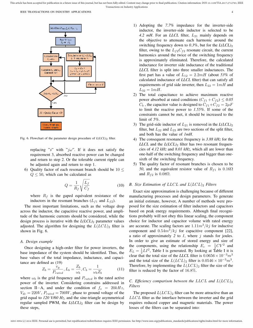
Fig. 6. Flowchart of the parameter design procedure of L(LCL)2 filter.
replacing ”s” with ”jω”. If it does not satisfy the
requirement 3, absorbed reactive power can be changed
and return to step 2. Or the tolerable current ripple can
be adjusted again and return to step 1.
6) Quality factor of each resonant branch should be 10 ≤Q ≤ 50, which can be calculated as
Q =1
Rf
√
Lf
Cf
(10)
where Rf is the gaped equivalent resistance of the
inductors in the resonant branches (Lf1 and Lf2).
The most important limitations, such as the voltage drop
across the inductor, the capacitive reactive power, and ampli-
tude of the harmonic currents should be considered, while the
design process is iterative with the L(LCL)2 parameter values
adjusted. The algorithm for designing the L(LCL)2 filter is
shown in Fig. 6.
A. Design example
Once designing a high-order filter for power inverters, the
base impedance of the system should be identified. Thus, the
base values of the total impedance, inductance, and capaci-
tance are defined as (19)
Zb =vg
Prated
, Lb =Zb
ωb
, Cb =1
ωbZb
(11)
where ωb is the grid frequency and Prated is the rated active
power of the inverter. Considering constrains addressed in
section II−A, and under the condition of fs = 20kHz,
Vdc = 220V , Prated = 700W , phase to ground voltage of the
grid equal to 120 V/60 Hz, and the sine-triangle asymmetrical
regular sampled PWM, the L(LCL)2 filter can be design by
these steps,
1) Adopting the 7.7% impedance for the inverter-side
inductor, the inverter-side inductor is selected to be
4.2 mH. For an LLCL filter, L21 mainly depends on
the objective to attenuate each harmonic around the
switching frequency down to 0.3%, but for the L(LCL)2filter, owing to the Lf2Cf2 resonate circuit, the current
harmonics around the twice of the switching frequency
is approximately eliminated. Therefore, the calculated
inductance for inverter side inductance of the traditional
LLCL filter is split into three smaller inductances. The
first part has a value of L12 = 2.2mH (about 53% of
calculated inductance of LLCL filter) that can satisfy all
requirements of grid side inverter, then L22 = 1mH and
L32 = 1mH .
2) The total capacitance to achieve maximum reactive
power absorbed at rated conditions (Cf1 +Cf2) ≤ 0.05
Cb , the capacitor value is designed to Cf1+Cf2 = 2µFto limit the reactive power to 1.55%. If some of the
constraints cannot be met, it should be increased to the
limit of 5%.
3) The grid-side inductor of L21 is removed in the L(LCL)2filter, but L22 and L23 are two sections of the split filter,
and both has the value of 1mH.
4) The consequent resonance frequency is 3.88 kHz for the
LLCL and the L(LCL)2 filter has two resonant frequen-
cies of 4.12 kHz and 8.01 kHz, which all are lower than
one-half of the switching frequency and bigger than one-
sixth of the switching frequency.
5) The quality factor of resonant branches is chosen to be
50, and the equivalent resistor value of Rf1 is 0.16Ωand Rf2 is 0.08Ω.
B. Size Estimation of LLCL and L(LCL)2 Filters
Exact size approximation is challenging because of different
manufacturing processes and design parameters. To generate
an initial estimate, however, A number of methods were pro-
posed for the size estimation of filter inductors and capacitors
based on peak energy requirements. Although final recogni-
tions probably will not obey this linear scaling, the component
choice for inductor and capacitor volume with rated energy
are accurate. The scaling factors are 1.11m3/kj for inductive
component and 0.54m3/kj for capacitive component [22],
a ratio of approximately 2 to 1, where j stands for joules.
In order to give an estimate of stored energy and size of
the components, using the relationship Ec = 12CV 2 and
EL = 12LI
2, Table I is generated. By looking at Table I it is
clear that the total size of the LLCL filter is 0.0656×10⁻³m3
and the total size of the L(LCL)2 filter is 0.0546× 10⁻³m3.
Therefore, by implementing the L(LCL)2 filter the size of the
filter is reduced by the factor of 16.8%.
C. Efficiency comparison between the LLCL and L(LCL)2Filters
The proposed L(LCL)2 filter can be more attractive than an
LLCL filter as the interface between the inverter and the grid
requires reduced copper and magnetic materials. The power
losses of the filters can be separated into:
0093-9994 (c) 2016 IEEE. Personal use is permitted, but republication/redistribution requires IEEE permission. See http://www.ieee.org/publications_standards/publications/rights/index.html for more information.
This article has been accepted for publication in a future issue of this journal, but has not been fully edited. Content may change prior to final publication. Citation information: DOI 10.1109/TIA.2017.2712783, IEEETransactions on Industry Applications
IEEE TRANSACTIONS ON INDUSTRY APPLICATIONS 5
TABLE ISIZE ESTIMATION OF LLCL AND L(LCL)2 FILTERS
Components Energy Stored in Size of
the Components (j) the components (m3)
L11 + L12 0.0919 0.0496 × 10⁻³
Lf 1.29 × 10⁻⁷ 0.6966 × 10⁻¹⁰
Cf 0.0144 0.016 × 10⁻³
L12 + L22 + L32 0.0715 0.0386 × 10⁻³
Lf1 + Lf2 8.09 × 10⁻⁸ 4.3686 × 10⁻¹¹
Cf1 + Cf2 0.0144 0.016 × 10⁻³
1) High-frequency passive damping loss, which can be
obtained as follows
Pd(ripple) =1
2|IAM (n, k1)|
2×Rf1 + |IAM (n, k2)|2×Rf2
(12)
where n = ±1,±3,±5, k1 = 1 and k2 = 2.
Passive Damping (PD) techniques use a resistance con-
nected in series with the capacitor in order to attenuate the
LC branch resonance at the cost of curtailing efficiency [23].
Lossless Active Damping (AD) methods with virtual resistors
have been widely explored to suppress these oscillations. By
using this technique, a resistance damping characteristic em-
ulated in the lossless method, and no resistance is physically
connected to the circuit [24]. Therefore, when using active
damping method, Pd can be set to zero.
2) Power losses in inductors, can be separated into Pcore
(core loss) and Pcopper (copper loss)
Pcore = k(fαBβVe) (13)
where k, α, and β are material parameters generally found
by curve fitting; B is the flux density, in Tesla and Ve is the
magnetic core volume, in cm3.
Pcopper = IfR2dc + IacR
2ac (14)
where If is the RMS value of the fundamental frequency
current component and Iac is the RMS value of the ac-ripple
current component. it can be assumed that Rac = Rdc in this
study. The power loss and efficiency values of the L(LCL)2filter and the LLCL filter for both PD and AD methods are
presented in Table II. It can be seen that the efficiency is
increased by 0.169% (for PD method) and 0.173% (for AD
method) compared to that of the LLCL filter.
The total loss of the LLCL and L(LCL)2 filters are
measured in our hardware prototype by means of a LaCroy
WaveRunner 64Xi, 600 MHz Oscilloscope. The measured
output power was 691.55 watts for the LLCL and 692.74
watts for L(LCL)2 filter. The input power of both filters
(which is the output power of the VSC) was 697.27 watts. The
values in Table II are based on calculation, but the measured
values of efficiencies are 99.17% and 99.35% for LLCL and
L(LCL)2, respectively. Therefore, the measured total power
losses for the LLCL filter and the L(LCL)2 filter are higher
in value by a factor of 8.54 % and 10.63 %, respectively,
comparing to calculated losses.
III. SIMULATION AND EXPERIMENTAL RESULTS
In order to confirm the effectiveness of the proposed
L(LCL)2 filter on suppressing the current harmonics, a 700-W
TABLE IICALCULATED POWER LOSSES AND EFFICIENCY OF THE L(LCL)2
FILTER AND THE LLCL FILTERS BASED ON NOMINAL OUTPUT POWER OF
700W.
LLCL L(LCL)2
Pd 0.0064w 0.0345w
Pcopper 3.4432w 2.7593w
Pcore 1.8238w 1.3015w
Total Loss(PD) 5.2735w 4.0953w
Total Loss(AD) 5.2671w 4.0608w
Efficiency(PD) 99.247% 99.415%
Efficiency(AD) 99.248% 99.420%
vg:[50V/div]
ig:[5A/div]
Time: 5ms/div
(a)
(b)
(c)Fig. 7. LLCL filter. (a) Grid voltage and grid-side current waveforms. (b)Power density spectrum of grid-side current (Experimental setup). (c) Powerdensity spectrum of grid-side current (Simulation)
prototype of the single-phase full-bridge grid-tied inverter with
the ”STM32F4” Microcontroller is constructed. In addition,
a Matlab Simulink-based study is carried out to assess the
experimental analysis. The experimental parameters of the
filter are the same as those for simulations listed in Table
III.
The experiments are evaluated and investigated under the
given conditions of fs = 20kHz, Vdc = 220V , vg =120V/60Hz, Prated = 700W , and SPWM strategy is used
in the inverter and the dc-link voltage is kept at 220V .
Case I is the traditional LLCL filter strategy and Case II is
the L(LCL)2 filter strategy with an extra trap at 40kHz. Figs.
7-11 show important system measurements that are captured
by a LaCroy WaveRunner 64Xi oscilloscope in experimental
tests and Matlab Simulink plots.

0093-9994 (c) 2016 IEEE. Personal use is permitted, but republication/redistribution requires IEEE permission. See http://www.ieee.org/publications_standards/publications/rights/index.html for more information.
This article has been accepted for publication in a future issue of this journal, but has not been fully edited. Content may change prior to final publication. Citation information: DOI 10.1109/TIA.2017.2712783, IEEETransactions on Industry Applications
IEEE TRANSACTIONS ON INDUSTRY APPLICATIONS 6
vg:[50V/div]
ig:[5A/div]
Time: 5ms/div
(a)
(b)
(c)Fig. 8. L(LCL)2 filter. (a) Grid voltage and grid-side current waveforms. (b)Power density spectrum of grid-side current (Experimental setup). (c) Powerdensity spectrum of grid-side current (Simulation).
Figs. 7 and 8 show the grid side current-voltage waveforms
and the power density spectrum of the grid-side current for
cases I and II, respectively. Figs. 7(b) and Fig. 8(b) illustrate
that the amplitude of the dominant harmonic current at 20
kHz is reduced by 8.80 dB/HZ from case I to case II, but
at 40 kHz it increased from -102.37 dB/Hz (case I) to -
97.01 dB/Hz (case II). Therefore, the most dominant current
harmonics are diminished even more than the previous design.
However, a small increase occurred at the double of the
switching frequency, but as the power density is too small (-
97.01 dB/Hz), it can be neglected. Thus, the size of the filter is
reduced, and as a result, the total loss is decreased. In addition,
the performance of the filter is improved. Figs. 7 (c) and 8
(c) show the simulation results of the power density spectrum
of the grid-side current. As it can be seen, the experimental
results are in accordance with the simulation graphs.
The currents flowing through the resonant branches for Case
I and Case II are shown in Figs. 9 to 11 while the grid current
is 5.8 A and the voltage is 120 V. The magnitude of the currents
in Lf1Cf1 and Lf2Cf2 traps are almost half of LfCf trap and
that is because the impedance of both traps of L(LCL)2 filter
is 2.652kΩ (at 60 Hz), but the LLCL filter has an impedance
of 1.326 kΩ. Also, it can be seen that the power density of
current harmonics at the switching frequency and multiples
of the switching frequency are almost the same in the LfCf
branch of the LLCL and Lf1Cf1 branch of the L(LCL)2 filter.
(a)
(b)
(c)Fig. 9. (a) LfCf current of LLCL filter . (b) Power spectral density of LfCf
current in LLCL filter (Experimental setup). (b) Power spectral density ofLfCf current in LLCL filter (Simulation).
In addition to that more attenuation occurs at Lf2Cf2. Then,
in Figs. 9 (c) - 11 (c) simulation results are depicted which
are quite close to the hardware experimental results.
The measured total harmonic distortion (THD)% of igin Cases I, and II are 3.72% and 2.94% which shows the
effectiveness of the designed filter in improving the THD of
the grid current.
At last, the response of the developed filter is compared with
that of an LLCL-based inverter in terms of voltage regulation.
In order to do that, the simulations were run at a sampling time
of 2µs and the values of Table III. These values were designed
such that the performance of the L(LCL)2 filter is comparable
to that of the LLCL in terms of steady state performance and
the dynamic response. Fig. 12 shows both cases when a 0.5puload is switched in at the point of grid connection on t =0.15s. It can be seen that the inverter maintains a constant dc-
link voltage before and after the change. Results show that,
replacing the LLCL filter with an L(LCL)2 filter improves
the dynamic performance of the inverter mainly due to the
reduction of dc-link voltage fluctuations.
The experimental setup of the L(LCL)2-filter-based inverter
system is shown in Fig. 13. For building the inductances of
LLCL and L(LCL)2 filters Ferrite cores with N87 material and
epoxy coating is used.

0093-9994 (c) 2016 IEEE. Personal use is permitted, but republication/redistribution requires IEEE permission. See http://www.ieee.org/publications_standards/publications/rights/index.html for more information.
This article has been accepted for publication in a future issue of this journal, but has not been fully edited. Content may change prior to final publication. Citation information: DOI 10.1109/TIA.2017.2712783, IEEETransactions on Industry Applications
IEEE TRANSACTIONS ON INDUSTRY APPLICATIONS 7
(a)
(b)
(c)Fig. 10. (a) Current of switching frequency trap Lf1Cf1 of L(LCL)2 filter.(b) Power spectral density of Lf1Cf1 current in L(LCL)2 filter (Experimentalsetup). (c) Power spectral density of Lf1Cf1 current in L(LCL)2 filter(Simulation).
A. Analysis and Discussion
From the simulation and experimental results, the following
can be seen.
1) In both cases, dominating harmonic current meets the
recommendation of IEEE 519-2014 in the experiment,
however, the 20kHz current harmonic reduced and the
40kHz current harmonic has the same value.
2) The value of the grid-side inductor is reduced in cases
II, so the voltage drop during the operation and thereby
the dc link voltage are the same.
3) The value of the total inductor of L(LCL)2 filter is
reduced by a factor of 22.22%, compared to that of the
LLCL filter.
4) The reactive power in the newly designed filter is the
same as the traditional LLCL filter Cf1 + Cf2 = Cf .
5) In general, the experimental results are in acceptable
agreement with the theoretical study, particularly with
regard to the harmonic current attenuation around the
switching frequency and the double of the switching
frequency.
B. Close-Loop Stability Analysis of the Current Controller
The eigenvalue analysis is one of the suitable techniques
that can be used for the stability analysis of a system. Fig. 14
illustrates the general block diagram of a current controller,
(a)
(b)
(c)Fig. 11. (a) Current of the double of switching frequency trap Lf2Cf2 ofL(LCL)2 filter . (b) Power spectral density of Lf2Cf2 current in L(LCL)2filter (Experimental setup). (c) Power spectral density of Lf2Cf2 current inL(LCL)2 filter (Simulation).
Fig. 12. DC Link voltage when a 0.5 pu load is switched-in on t=0.15.
where P(s), C(s), and G(s) are the model of the controller,
inverter, and proposed filter, respectively. A conventional PI
controller is adopted as P(s) to obtain the dynamics, i.e.
P (s) =(kps+ kI)
s. (15)
where kp = 1 is proportional gain and kI = 100 is the
integral gain. These values are designed and tuned by the trial
and error method. It is assumed that the time delays in the
system because of the phasor PWM blocks are negligible, i.e.,
C(s)=1, and G(s) is calculated by (3). Therefore, the closed-

0093-9994 (c) 2016 IEEE. Personal use is permitted, but republication/redistribution requires IEEE permission. See http://www.ieee.org/publications_standards/publications/rights/index.html for more information.
This article has been accepted for publication in a future issue of this journal, but has not been fully edited. Content may change prior to final publication. Citation information: DOI 10.1109/TIA.2017.2712783, IEEETransactions on Industry Applications
IEEE TRANSACTIONS ON INDUSTRY APPLICATIONS 8
Fig. 13. Experimental Setup
TABLE IIIPARAMETERS USED FOR SIMULATIONS
Elements Parameters Values
Inverter DC link voltage (Vdc) 220 V
Switching frequency (fs) 20 kHz
Rated power (Prate) 700 w
AC Grid Grid phase voltage (Vg) 120 V
Grid frequency (f0) 60 Hz
LLCL2 Filter Converter side inductor (L12) 2.2mH
Grid side inductors (L22 = L32) 1 mH
Resonant circuit inductor (Lf1) 63.3µHResonant circuit inductor (Lf2) 15.83µH
Resonant circuit capacitors (Cf1 = Cf2) 1µFEquivalent resistance of the inductor (Rf1) 0.16ΩEquivalent resistance of the inductor (Rf2) 0.08Ω
LLCL Filter Converter side inductor (L11) 4.2 mH
Grid side inductor (L21) 1.2 mH
Resonant circuit inductor (Lf ) 31.67µHResonant circuit capacitor (Cf ) 2µF
Equivalent resistance of the inductor (Rf ) 0.11Ω
P(s) C(s) G(s)
Plant Model
*
gi g
ii
v
Fig. 14. Block diagram of the current control system.
loop transfer function of the current control system can be
written as
H(s) =ig(s)
i∗g(s)=
P (s)G(s)
1 + P (s)G(s)(16)
The bandwidth of a closed-loop control system is defined as
the frequency range where the magnitude of the closed loop
gain does not drop below -3 dB, as shown in Fig 15. As can
be seen, the bandwidth of closed-loop transfer function of the
current controller with the proposed L(LCL)2 filter is around
120 Hz.
It is assumed that the time delays in the system because
of the phasor PWM blocks are negligible. The eigenvalues
of the closed-loop transfer function determine the dynamics
of the closed-loop system. Here, the stability of the proposed
system, with respect to the variation in the proposed L(LCL)2parameters, is studied. This study is based on a 700 w
laboratory prototype, in which parameters are summarized in
Table I. The eigenvalues of the system at this operating point
Frequency (Hz) : 120
Magnitude (dB) : =3.01
12
0 H
z
-3 dB
Bandwidth
Fig. 15. Closed-loop frequency response of the current controller indicatingthe bandwidth and the cutoff frequency.
are λ1,2 = −118.78 ± j99.22, λ3,4 = −286.43 ± j25867.9,
and λ5,6 = −1403.46 ± j50321.53. The real parts of all six
eigenvalues are negative, which betokens the stability of the
linearized system. However, the stability of the overall system
cannot be guaranteed for all values of the filter parameters.
Thus, for stability analysis, the eigenvalues of the system are
plotted versus the variation of one parameter at a time, while
the other nominal parameters remain constant.
It should be noted that the range variation of all filter
parameters correspond to the step by step design procedure
discussed in Section III. Moreover, in transfer function (16),
with ±20% variations of the Lf1 and the Lf2, the system
eigenvalues remain almost constant. Indeed, the variation of
Lf1 and Lf2 does not affect the stability of the proposed
system.
Fig. (16a) and Fig. (16b) show the impacts of L12 and
L32 on the eigenvalues of the system, respectively, when L1
varies from 1.39 mH to 2.52 mH and L32 varies from 0.84
mH to 1.485 mH. Since L22 is equal to L32, their variations
are depicted together in Fig. (16b). It can be observed that
the increase of the converter-side and the grid-side inductance
moves all eigenvalues into the vertical axis. Thus, once L12
and L32 increase, it is expected that the overall system
response becomes longer and less oscillatory.
The variation of the system eigenvalues by varying the Cf1
and Cf2 from 0.5 µF to 3 µF are shown in Fig. (16c) and
Fig. (16d). As can be seen, the impact of the Cf1 and Cf2
on the eigenvalues λ1 and λ2 are almost negligible. However,
Fig. (16c) depicts that complex eigenvalues λ3, λ4, λ5, and
λ6 move into the real axis, which can decrease the natural
frequencies of the system and increases the damping factor of
the system. Fig. (16d) determines that all eigenvalues stay on
the left half of the s-plane for the whole operating range that
demonstrates the stability of the system over the given range.
Figs. (16e) and (16f) illustrate the eigenvalues of the pro-
posed system as Rf1 and Rf2 vary from 0.08 Ω to 0.39 Ωand 0.16 Ω to 0.8 Ω, respectively. As can be seen, increasing
the resistances of the filter moves the real part of eigenvalues
λ3, λ4, λ5, and λ6 toward the left, resulting in faster response
and less oscillatory.
C. Small-signal model of the dc-link dynamics considering
the instantaneous power for bi-directional ac/dc power flow
applications
If the L(LCL)2 filter is employed in bi-directional ac/dc
power flow applications, the converter should be able to

0093-9994 (c) 2016 IEEE. Personal use is permitted, but republication/redistribution requires IEEE permission. See http://www.ieee.org/publications_standards/publications/rights/index.html for more information.
This article has been accepted for publication in a future issue of this journal, but has not been fully edited. Content may change prior to final publication. Citation information: DOI 10.1109/TIA.2017.2712783, IEEETransactions on Industry Applications
IEEE TRANSACTIONS ON INDUSTRY APPLICATIONS 9
(a) (b)
1
2
3
4
6
5
(c)
1
2
3
4
6
5
(d)
1
2
3
4
6
5
(e)
1
2
3
4
6
5
(f)
Fig. 16. Root locus of the closed-loop transfer function of the current controller (Hs) as (a) L12 varies from 1.39mH to 2.52mH (b) L22 and L32 vary from0.84mH to 1.485mH (c) Cf1 varies from 0.5µF to 3µF (d) Cf2 varies from 0.5µF to 3µF (e) Rf1 varies from 0.08Ω to 0.39Ω. (f) Rf2 varies from 0.16Ωto 0.8Ω.
regulate dc voltage, and the instantaneous power stored in the
ac side filter affects the dc side dynamics. In this section, the
small-signal model of the dc-link dynamics considering the
instantaneous power is studied.
In high-order ac-side filters applications, e.g. LCL, LLCLor L(LCL)2 filter due to the frequency-scale separation of the
high order filter dynamics and dc-link voltage dynamics, the
filter has a negligible effect on the dc-link voltage dynamics.
The fundamental frequency is normally higher than the band-
width of the dc-link voltage control loop (between 20 to 50
Hz). The high order ac-side filter acts mainly as an L filter
(L12 + L22 + L32) [25].
The dc-link dynamics’ model can be obtained when the total
instantaneous power in storage devices, i.e., LDC−eq and Ceq
are considered. The calculations on this section are based on
[26] and [27]. Ceq and LDC−eq are the equivalent capacitance
and inductance reflected to the dc side VSC, respectively. The
power balance across the dc-link capacitor can be given by:
Pext − Ploss −V 2DC
RL
−D(
0.5LDC−eqI2DC
)
− D(0.5CeqV2DC) = PDC = Pt (17)
where IDC is the current of the dc inductor; Pext is the
external injected power to the dc side; Ploss is the losses
in the converter; RL is the VSC reflected dc side equivalent
static resistance; PDC is the net power as shown in Fig 2,
that is equivalent to the VSC ac-side power Pt; and the time-
derivative operator is represented by D - i.e., Dx = d(x)/dt.Consider that Pt does not have the same value of the grid
injected power (Ps), because of the ac-side filter.
By using similar calculation in [26] and letting x1 = VDC
and x2 = DVDC; the power balance equation can be calculated
as follows
Pext − Ploss − PDC − LDC−eqCeqPDC−0
VDC−nominalDx2
− LDC−eqPDC−0
V 2DC−nominal
DPDC
+ LDC−eq
P 2DC−0
V 3DC−nominal
x2 − CeqVDC−nominalx2
−2VDC−nominal
Rp
x1 = 0. (18)
where ˜ indicates the perturbed signal around the equilibrium
point (E.P.) of each variable. Moreover, the equilibrium point
(E.P.) can be expressed by (19) taken into account that all
variables are static at the equilibrium situation
(E.P.) = (x1−0, x2−0, Dx2−0PDC−0, DPDC−0, Pext−0,
Ploss−0) = (VDC−nominal, 0, 0, PDC−0, 0, Pext−0, Ploss−0) (19)
According to the equation (18), with the purpose of reaching
a linear time-invariant (LTI) model that can describe the
connection between the output VDC and the control input Ig ,
a formula which connects PDC to the control input Ig have
to be calculated.

0093-9994 (c) 2016 IEEE. Personal use is permitted, but republication/redistribution requires IEEE permission. See http://www.ieee.org/publications_standards/publications/rights/index.html for more information.
This article has been accepted for publication in a future issue of this journal, but has not been fully edited. Content may change prior to final publication. Citation information: DOI 10.1109/TIA.2017.2712783, IEEETransactions on Industry Applications
IEEE TRANSACTIONS ON INDUSTRY APPLICATIONS 10
Therefore, studying the total power balance on the ac side is
necessary for analyzing the instantaneous power of the ac-side
filter. This power balance is defined as follows
PDC = Pt = Ploss R + Pfilter L + Ps (20)
where Ploss R is the total instantaneous power loss in the
equivalent resistance of the inductor L12, L22 and L32, PlossL
is the total instantaneous power of the ac-side inductor (L12+L22+L32) , and Ps is the total absorbed/injected instantaneous
power at the point of common coupling (PCC) for stabilizing
the dc-link voltage. The total absorbed instantaneous power
by a single phase network can be shown by
Psingle phase network = Re
~v(t)~i∗(t)
(21)
the total stored energy in filter inductors is expressed by
WL = 0.5(L12 + L22 + L32)(i2g) (22)
where ig is the current injected into the inductors L12, L22 and
L32. As a result, (23) is the expression of the instantaneous
power of filter series inductors.
Pfilter L = (L12 + L22 + L32)igDig. (23)
and Ps can be calculated by:
Ps = IgVgs (24)
where Vgs is the voltage space vector at the PCC. Using (20)
- (24), the relationship between PDC , Ig can be shown by
PDC − (L12 + L22 + L32)igDig −R(Ig)2 − IgVgs
= G(Ig, DIg) = 0. (25)
Equation (25) is nonlinear, therefore the Taylor series expan-
sion around one E.P. is applied on the dynamic function Gas
G(Ig, DIg) = G|(E.P.)+∂G
∂Ig|(E.P.)Ig
+∂G
∂DIg|(E.P.)DIg + H.O.T.. (26)
The E.P. of (26) can be shown by
(E.P.) = (Ig−0, DIg−0) = (Ig−0, 0). (27)
After mathematical manipulation, (28) can be reached.
PDC = LIg−0DIg +RIg−0Ig + Vgs Ig. (28)
In addition to (28), DPDC is also required to find the explicit
transfer function between Ig and VDC using (18). Using (28),
DPDC and its E.P. can be given by
DPDC − (L12 + L22 + L32)((DIg)2 + IgD
2Ig)
− 2RIgDIg − VgsDIg
= H(Ig, DIg, D2Ig) = 0 (29)
(E.P.) = (Ig−0, DIg−0, D2Ig−0)
= (Ig−0, 0, 0). (30)
By implementing the Taylor series expansion on the function
H in (29), DPDC can be calculated by
DPDC = (L12 + L22 + L32)Ig−0D2Ig +RIg−0DIg
+ VgsDIg. (31)
By combining the equations (18), (28), and (31), the relation-
ship between Ig and VDC is reached as follows
VDC =Pext − Ploss
As2 +Bs+ E−
as2 + bs+ e
As2 +Bs+ EIg
a∆= −LDC−eq(L12 + L22 + L32)
PDC−0Ig−0
V 2DC−nominal
b∆= −(L12 + L22 + L32)Ig−0
− LDC−eqPDC−0
V 2DC−nominal
(RIg−0 + Vgs)
e∆= −RIg−0 − Vgs
A∆= LDC−eqCeq
PDC−0
VDC−nominal
B∆=
(
CeqVDC−nominal − LDC−eq
P 2DC−0
V 3DC−nominal
)
E∆=
(
2
RL
VDC−nominal
)
(32)
In many different references, e.g. [28], the effect of the
dc filter is not taken into consideration, while the ac filter
instantaneous power is reflected into the dynamic analysis of
the dc-link voltage. In that situation, LDC−eq is set to zero
which results in (33) becoming a special case of (32). The
values of a, b, e, A, B, and E are given in (33) for LDC−eq = 0.
a = 0
b = −(L12 + L22 + L32)Ig−0
e∆= −RIg−0 − Vgs
A = 0 then
VDC =−(L12 + L22 + L32)Ig−0s− Vgs −RIg−0
CeqVDC−nominals+2
RLVDC−nominal
Ig
− Disturbance Signals.
B = CeqVDC−nominal
E =2
RL
VDC−nominal (33)
In (33), in both rectification and inversion modes, the magni-
tude of the linearized plant is the same. On the other hand,
in the rectification mode, the phase is dramatically reduced at
the same power, due to the right-hand-plane (RHP) zero. If
the time constant of the current controller is equal to zero, in
order to have a stable transfer function B and E in (33) should
be positive. As Ceq, VDC−nominal and RL are always positive
numbers, (33) is always stable in bidirectional ac/dc power
flow application.
IV. CONCLUSION
In this paper, the principle of the conventional LLCL filter
and parameter design of the L(LCL)2 filters has been proposed.
Since grid-side inductance (L21) of the LLCL filter is mainly
decided by the harmonic currents around the double of the

0093-9994 (c) 2016 IEEE. Personal use is permitted, but republication/redistribution requires IEEE permission. See http://www.ieee.org/publications_standards/publications/rights/index.html for more information.
This article has been accepted for publication in a future issue of this journal, but has not been fully edited. Content may change prior to final publication. Citation information: DOI 10.1109/TIA.2017.2712783, IEEETransactions on Industry Applications
IEEE TRANSACTIONS ON INDUSTRY APPLICATIONS 11
switching frequency instead of those around the switching
frequency, it has been replaced by a small trap at double of the
switching frequency. Compared to the LLCL filter, this replace-
ment results in the reduction of the total inductance size and
hence the total loss of the filter. The inverter side inductance is
divided into three parts to place resonant branches in between
them. Therefore, the L(LCL)2 filter has less copper loss and
better performance at high order harmonics attenuation. In
the proposed design, the maximum power factor variation
remained unchanged and the THD has improved by 18.61%.
A 700 W single-phase grid-tied inverter is designed to
compare the characteristics of the conventional LLCL filter
and the suggested L(LCL)2 filter through experimental results.
The results validate the value of the inductors of the L(LCL)2filter, which is reduced by a factor of 22.22%, compared to
that of the LLCL filter, when the modulation index is 0.9.
Closed loop stability analysis of the current controller
and the small-signal model of dc-link dynamics considering
the instantaneous power for bi-directional ac/dc power flow
applications have shown that the filter can perform stably in
the same ranges of the LLCL filter.
REFERENCES
[1] A. Anzalchi and A. Sarwat, “Analysis of carbon tax as an incentivetoward building sustainable grid with renewable energy utilization,”in Green Technologies Conference (GreenTech), 2015 Seventh Annual
IEEE, April 2015, pp. 103–109.
[2] A. Anzalchhi and A. Sarwat, “Artificial neural network based duty cycleestimation for maximum power point tracking in photovoltaic systems,”in SoutheastCon 2015, April 2015, pp. 1–5.
[3] N. Harischandrappa and A. K. S. Bhat, “A fixed-frequency lcl -typeseries resonant converter with a capacitive output filter using a modifiedgating scheme,” IEEE Transactions on Industry Applications, vol. 50,no. 6, pp. 4056–4064, Nov 2014.
[4] M. Lindgren and J. Svensson, “Connecting fast switching voltagesource converters to the grid-harmonic distortion and its reduction,” inStockholm Power Tech. Conf., June 18-22 1995, pp. 191–195.
[5] M. Liserre, F. Blaabjerg, and S. Hansen, “Design and control of anlcl-filter-based three-phase active rectifier,” Industry Applications, IEEE
Transactions on, vol. 41, no. 5, pp. 1281–1291, Sept 2005.
[6] I. Gabe, V. Montagner, and H. Pinheiro, “Design and implementationof a robust current controller for vsi connected to the grid through anlcl filter,” Power Electronics, IEEE Transactions on, vol. 24, no. 6, pp.1444–1452, June 2009.
[7] A. Reznik, M. G. Sim?es, A. Al-Durra, and S. M. Muyeen, “Lcl filterdesign and performance analysis for grid-interconnected systems,” IEEE
Transactions on Industry Applications, vol. 50, no. 2, pp. 1225–1232,March 2014.
[8] A. Houari, H. Renaudineau, J. P. Martin, B. Nahid-Mobarakeh,S. Pierfederici, and F. Meibody-Tabar, “Large-signal stabilization of acgrid supplying voltage-source converters with lcl-filters,” IEEE Trans-
actions on Industry Applications, vol. 51, no. 1, pp. 702–711, Jan 2015.
[9] P. Channegowda and V. John, “Filter optimization for grid interactivevoltage source inverters,” Industrial Electronics, IEEE Transactions on,vol. 57, no. 12, pp. 4106–4114, Dec 2010.
[10] Y. Jiao, S. Lu, and F. Lee, “Switching performance optimization ofa high power high frequency three-level active neutral point clampedphase leg,” Power Electronics, IEEE Transactions on, vol. 29, no. 7, pp.3255–3266, July 2014.
[11] W. Wu, Y. Sun, Z. Lin, Y. He, M. Huang, F. Blaabjerg, and H.-H.Chung, “A modified llcl filter with the reduced conducted emi noise,”Power Electronics, IEEE Transactions on, vol. 29, no. 7, pp. 3393–3402,July 2014.
[12] W. Wu, Y. Sun, M. Huang, X. Wang, H. Wang, F. Blaabjerg, M. Liserre,and H.-H. Chung, “A robust passive damping method for llcl-filter-basedgrid-tied inverters to minimize the effect of grid harmonic voltages,”Power Electronics, IEEE Transactions on, vol. 29, no. 7, pp. 3279–3289,July 2014.
[13] W. Wu, Y. Sun, Z. Lin, T. Tang, F. Blaabjerg, and H.-H. Chung, “A newlcl -filter with in-series parallel resonant circuit for single-phase grid-tiedinverter,” Industrial Electronics, IEEE Transactions on, vol. 61, no. 9,pp. 4640–4644, Sept 2014.
[14] D. Pan, X. Ruan, C. Bao, W. Li, and X. Wang, “Capacitor-current-feedback active damping with reduced computation delay for improvingrobustness of lcl-type grid-connected inverter,” Power Electronics, IEEE
Transactions on, vol. 29, no. 7, pp. 3414–3427, July 2014.[15] D.Pan, X.Ruan, C.Bao, W.Li, and X.Wang, “Magnetic integration of
the lcl filter in grid-connected inverters,” Power Electronics, IEEE
Transactions on, vol. 29, no. 4, pp. 1573–1578, April 2014.[16] W. Wu, Y. He, and F. Blaabjerg, “An llcl power filter for single-phase
grid-tied inverter,” Power Electronics, IEEE Transactions on, vol. 27,no. 2, pp. 782–789, Feb 2012.
[17] A. Anzalchi, M. Moghaddami, A. Moghaddasi, A. I. Sarwat, and A. K.Rathore, “A new topology of higher order power filter for single-phasegrid-tied voltage-source inverters,” IEEE Transactions on Industrial
Electronics, vol. 63, no. 12, pp. 7511–7522, Dec 2016.[18] Y. Lang, D. Xu, S. Hadianamrei, and H. Ma, “A novel design method
of lcl type utility interface for three-phase voltage source rectifier,” inPower Electronics Specialists Conference, 2005. PESC ’05. IEEE 36th,June 2005, pp. 313–317.
[19] A. Anzalchi, M. Moghaddami, A. Moghaddasi, M. M. Pour, andA. Sarwat, “A modified higher order power filter for grid-connectedrenewable energy systems,” in 2016 IEEE/IAS 52nd Industrial and
Commercial Power Systems Technical Conference (I&CPS), May 2016,pp. 1–9.
[20] M. Liserre, F. Blaabjerg, and S. Hansen, “Design and control of anlcl-filter based three-phase active rectifier,” in Industry Applications
Conference, 2001. Thirty-Sixth IAS Annual Meeting. Conference Record
of the 2001 IEEE, vol. 1, Sept 2001, pp. 299–307 vol.1.[21] M. Huang, F. Blaabjerg, P. C. Loh, and W. Wu, “Stability analysis and
active damping for llcl-filter based grid-connected inverters,” in Power
Electronics Conference (IPEC-Hiroshima 2014 - ECCE-ASIA), 2014
International, May 2014, pp. 2610–2617.[22] J. Bloemink and T. Green, “Reducing passive filter sizes with tuned
traps for distribution level power electronics,” in Power Electronics
and Applications (EPE 2011), Proceedings of the 2011-14th European
Conference on, Aug 2011, pp. 1–9.[23] S. Sridharan and P. T. Krein, in 2015 IEEE International Electric
Machines Drives Conference (IEMDC).[24] K. Hatua, A. K. Jain, D. Banerjee, and V. T. Ranganathan, “Active
damping of output filter resonance for vector-controlled vsi-fed ac motordrives,” IEEE Transactions on Industrial Electronics, vol. 59, no. 1, pp.334–342, 2012.
[25] A. A. Rockhill, M. Liserre, R. Teodorescu, and P. Rodriguez, “Grid-filterdesign for a multimegawatt medium-voltage voltage-source inverter,”IEEE Transactions on Industrial Electronics, vol. 58, no. 4, pp. 1205–1217, April 2011.
[26] M. Davari and Y. A. R. I. Mohamed, “Dynamics and robust controlof a grid-connected vsc in multiterminal dc grids considering theinstantaneous power of dc- and ac-side filters and dc grid uncertainty,”IEEE Transactions on Power Electronics, vol. 31, no. 3, pp. 1942–1958,March 2016.
[27] Masoud Davari, “Dynamics, Robust Control, and Power Managementof Voltage-Source Converters in Hybrid Multiterminal AC/DC Grids,”Ph.D. dissertation, University of Alberta, Edmonton, Jan. 2016.[Online]. Available: https://era.library.ualberta.ca
[28] M. Davari and Y. A. R. I. Mohamed, “Variable-structure-based nonlinearcontrol for the master vsc in dc-energy-pool multiterminal grids,” IEEE
Transactions on Power Electronics, vol. 29, no. 11, pp. 6196–6213, Nov2014.

0093-9994 (c) 2016 IEEE. Personal use is permitted, but republication/redistribution requires IEEE permission. See http://www.ieee.org/publications_standards/publications/rights/index.html for more information.
This article has been accepted for publication in a future issue of this journal, but has not been fully edited. Content may change prior to final publication. Citation information: DOI 10.1109/TIA.2017.2712783, IEEETransactions on Industry Applications
IEEE TRANSACTIONS ON INDUSTRY APPLICATIONS 12
Arash Anzalchi (S’14) received his B.S. and M.S.degrees in Electrical Engineering from the K.N.Toosi University of Technology and Science andResearch Branch, I.A.U Tehran, Iran in 2007 and2011 respectively.
He is currently working as a Graduate Assistantpursuing his Ph.D. at Florida International Uni-versity, Miami, FL, USA. He is also one of theresearchers of the “Energy Power Reliability andAnalytic Center (EPRAC)”, which conducts high-end studies on the effect of high penetration PV in-
tegration into the Distribution Grid. His research interests include Photovoltaicintegration into the distribution grid, mitigation of power quality issues andsmart power electronic technologies for the renewable energy sources.
Masood Moghaddami (S’15) received the B.S.degree from Amirkabir University of Technology,Tehran, Iran, in 2009, the M.S. degree from IranUniversity of Science and Technology, Tehran, Iran,in 2012.
He is currently working toward the Ph.D. degreein the Department of Electrical and Computer En-gineering, Florida International University, Miami,Florida. From 2011 to 2014, he worked in the in-dustry as an engineer to design optimization of largepower transformers. His research interests include
finite element analysis, power electronics, contactless power transfer, andrenewable energy systems.
Amir Moghadasi (S’11)(M’16) received the B.Sc.degree in electrical engineering from Shaded Univer-sity, Tehran, Iran, in 2007, the M.Sc. degree in elec-trical engineering from Iran University of Scienceand Technology (IUST), Tehran, in 2009, and thePhD. Degree in electrical engineering from FloridaInternational University, Miami, FL, USA, in 2016.
Dr. Moghadasi is currently working as a Post-doctoral research associate at Florida InternationalUniversity. He is the lead researcher at FPL-FIUSolar Research Center to lead a research study on
analysis of the effects of real-time operating the 1.4 MW PV systemsinstalled at the FIU on the Florida, Power and Light (FPL) distribution circuit.His research interests are power electronics, design and control of powerconverters, high-penetration renewable systems, power quality, and applicationof computational intelligence techniques in power systems.
Maneli Malek Pour (S’15) received her Bachelor?sdegree in Computer Science from Shahid BeheshtiUniversity, Tehran, Iran. She is currently workingas a Graduate Research Assistant, pursuing her M.Sdegree in Department of Electrical and ComputerEngineering, Florida International University underthe supervision of Dr. Arif Sarwat. Her current re-search includes reliability analysis of Advanced Me-tering infrastructure meters(Temperature/Humidity),and life expectancy and accelerated aging of SmartGrid products and components. She is also interested
in Machine Learning and Data Mining Algorithms and techniques.
Arif I. Sarwat (M’08-SM’16) received the M.S.degree in electrical and computer engineering fromthe University of Florida, Gainesville, FL, USA, in2005, and the Ph.D. degree in electrical engineeringfrom the University of South Florida, Tampa, FL, in2010.
He worked in industry (SIEMENS) for nine years,executing many critical projects. Before joiningFlorida International University, Miami, FL, USA,as an Assistant Professor, he was an Assistant Pro-fessor of electrical engineering at the University at
Buffalo,State University of New York, Buffalo, NY, USA. His significantwork in energy storage, microgrid, and DSM is demonstrated by SustainableElectric Energy Delivery Systems in Florida. His research interests includesmart grids, high-penetration renewable systems, power system reliability,large-scale distributed generation integration, large-scale data analysis, cybersecurity, and vehicular technology.