archive 2011 - bits workshop · archive 2011 it’s a free for all! probing inside the socket marc...
TRANSCRIPT
22001111 Session 5
BiTS Workshop 2011 Archive
ARCHIVE 2011
IT’S A FREE FOR ALL!
Probing Inside the Socket Marc Moessinger—Verigy
Pin Grid Array Current Sense Interposer Application Featuring Vertical Embedded Resistors
Shaul Lupo, Omer Vikinski—Intel Corporation
PCB Pad Wear Analysis at 0.4mm Pitch - the story continues... Valts Treibergs, Christopher Cuda—Multitest
Thermal Testing - some tidbits from the lab James Forster—Wells-CTI
John Moore—Texas Instruments
COPYRIGHT NOTICE The papers in this publication comprise the pre-workshop Proceedings of the 2011 BiTS Workshop. They reflect the authors’ opinions and are reproduced here as they are planned to be presented at the 2011 BiTS Workshop. Updates from this version of the papers may occur in the version that is actually presented at the BiTS Workshop. The inclusion of the papers in this publication does not constitute an endorsement by the BiTS Workshop, the sponsors, BiTS Workshop LLC, or the authors.
There is NO copyright protection claimed by this publication. However, each presentation is the work of the authors and their respective companies: as such, it is strongly encouraged that any use reflect proper acknowledgement to the appropriate source. Any questions regarding the use of any materials presented should be directed to the author/s or their companies.
The BiTS logo and ‘Burn-in & Test Socket Workshop’ are trademarks of BiTS Workshop, LLC.
It’s a Free for All!
Session 5
2011 BiTS Workshop ~ March 6 - 9, 2011
Paper #11
2011T W E L F T H A N N U A L
Conference Ready 2/9/11
Probing Inside the Socket
2011 BiTS WorkshopMarch 6 - 9, 2011
Marc MoessingerVerigy
3/2011 Probing Inside the Socket 2
The challenge
• For Semiconductor Test Systems, the performance is usually specified at the interface between tester and DUT (Device Under Test) Board
• But the user would like to know the performance at the device, preferably directly at the device pins inside of the socket
It’s a Free for All!
Session 5
2011 BiTS Workshop ~ March 6 - 9, 2011
Paper #12
2011T W E L F T H A N N U A L
3/2011 Probing Inside the Socket 3
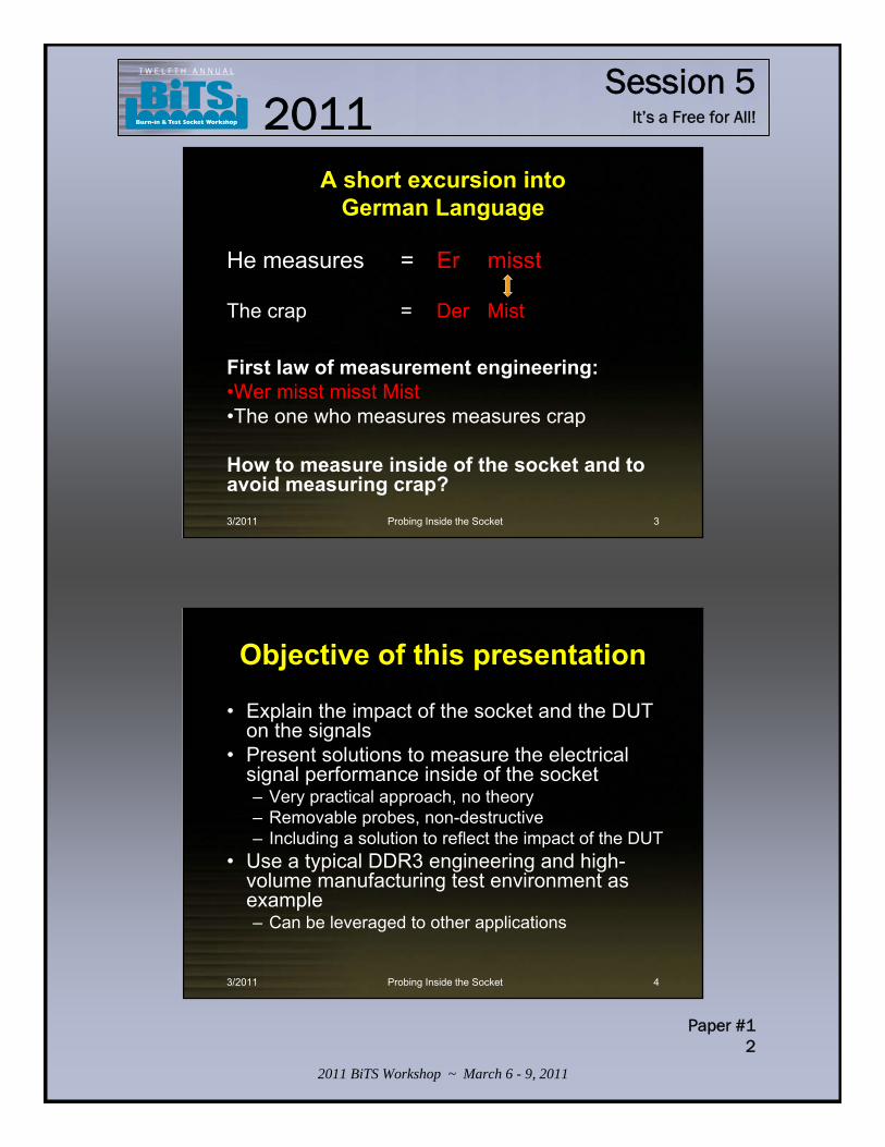
A short excursion intoGerman Language
He measures = Er misst
The crap = Der Mist
First law of measurement engineering:•Wer misst misst Mist•The one who measures measures crap
How to measure inside of the socket and to avoid measuring crap?
3/2011 Probing Inside the Socket 4
Objective of this presentation
• Explain the impact of the socket and the DUT on the signals
• Present solutions to measure the electrical signal performance inside of the socket– Very practical approach, no theory– Removable probes, non-destructive– Including a solution to reflect the impact of the DUT
• Use a typical DDR3 engineering and high-volume manufacturing test environment as example– Can be leveraged to other applications
It’s a Free for All!
Session 5
2011 BiTS Workshop ~ March 6 - 9, 2011
Paper #13
2011T W E L F T H A N N U A L
3/2011 Probing Inside the Socket 5
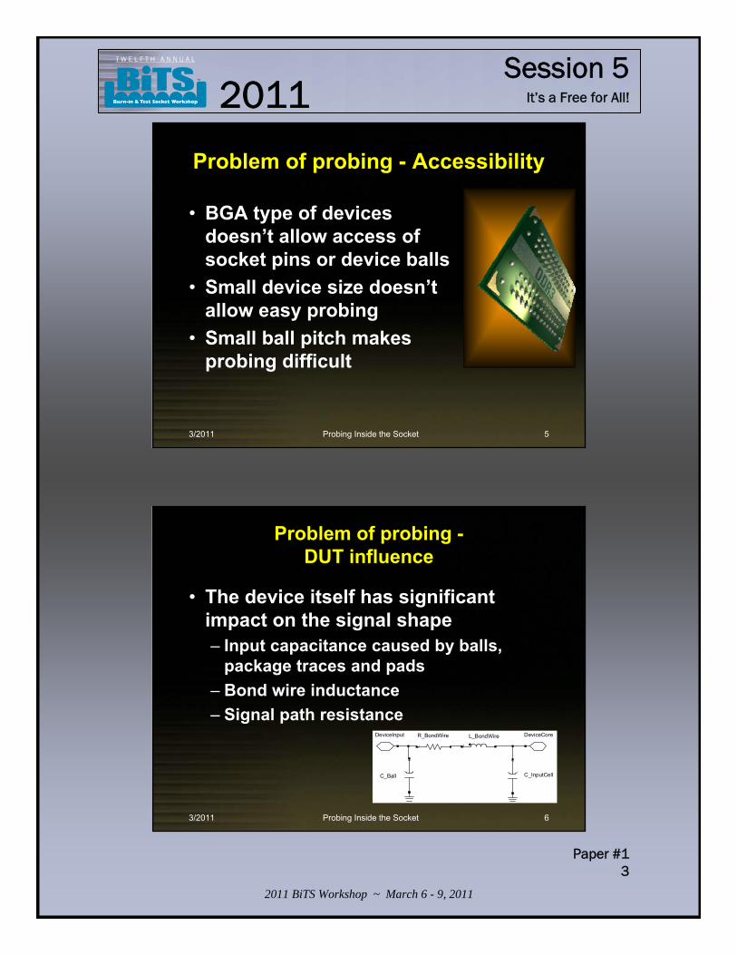
Problem of probing - Accessibility
• BGA type of devices doesn’t allow access of socket pins or device balls
• Small device size doesn’t allow easy probing
• Small ball pitch makes probing difficult
3/2011 Probing Inside the Socket 6
Problem of probing -DUT influence
• The device itself has significant impact on the signal shape– Input capacitance caused by balls,
package traces and pads– Bond wire inductance– Signal path resistance
C_Ball C_InputCell
DeviceCoreL_BondWireR_BondWireDeviceInput
It’s a Free for All!
Session 5
2011 BiTS Workshop ~ March 6 - 9, 2011
Paper #14
2011T W E L F T H A N N U A L
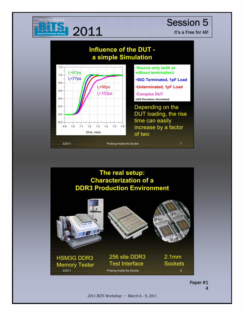
3/2011 Probing Inside the Socket 7
Influence of the DUT -a simple Simulation
•Source only (with or without termination)
•50Ω Terminated, 1pF Load
•Unterminated, 1pF Load
•Complex DUT(ADS Simulation, Normalized)
1.0 1.1 1.2 1.3 1.4 1.50.9 1.6
0.0
0.2
0.4
0.6
0.8
1.0
-0.2
1.2
time, nsec
Depending on the DUT loading, the rise time can easily increase by a factor of two
tr=67ps
tr=96ps
tr=77ps
tr=153ps
3/2011 Probing Inside the Socket 8
The real setup:Characterization of a
DDR3 Production Environment
HSM3G DDR3Memory Tester
256 site DDR3Test Interface
2.1mmSockets
It’s a Free for All!
Session 5
2011 BiTS Workshop ~ March 6 - 9, 2011
Paper #15
2011T W E L F T H A N N U A L
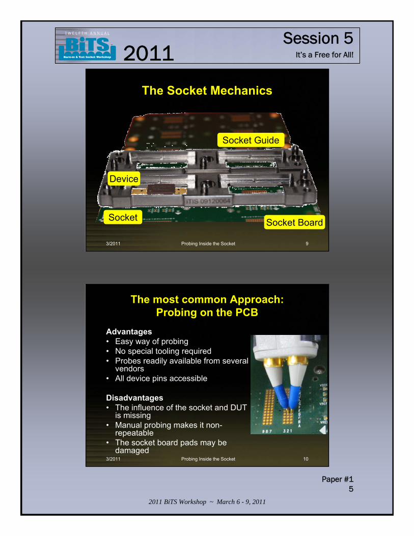
3/2011 Probing Inside the Socket 9
The Socket Mechanics
Socket BoardSocket
Socket Guide
Device
3/2011 Probing Inside the Socket 10
The most common Approach:Probing on the PCB
Advantages• Easy way of probing• No special tooling required• Probes readily available from several
vendors• All device pins accessible
Disadvantages• The influence of the socket and DUT
is missing• Manual probing makes it non-
repeatable• The socket board pads may be
damaged
It’s a Free for All!
Session 5
2011 BiTS Workshop ~ March 6 - 9, 2011
Paper #16
2011T W E L F T H A N N U A L
3/2011 Probing Inside the Socket 11
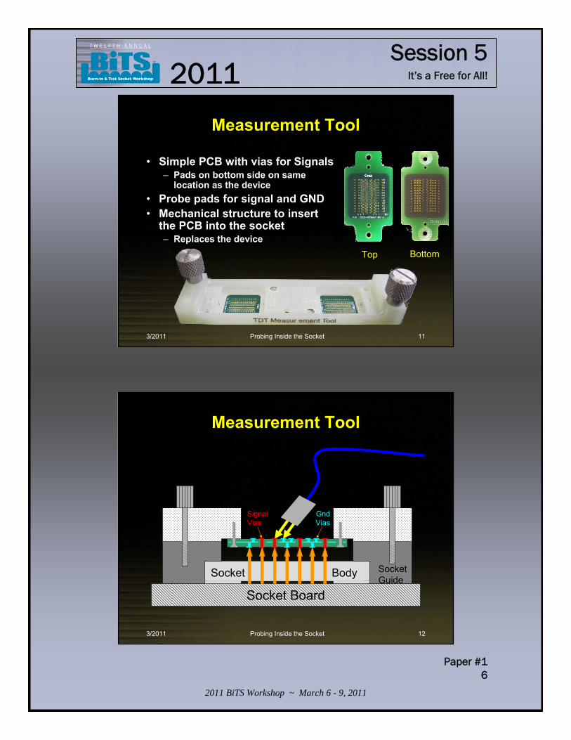
Measurement Tool
• Simple PCB with vias for Signals– Pads on bottom side on same
location as the device• Probe pads for signal and GND• Mechanical structure to insert
the PCB into the socket– Replaces the device
Top Bottom
3/2011 Probing Inside the Socket 12
Measurement Tool
Socket Body
Socket Board
SocketGuide
SignalVias
GndVias
It’s a Free for All!
Session 5
2011 BiTS Workshop ~ March 6 - 9, 2011
Paper #17
2011T W E L F T H A N N U A L
3/2011 Probing Inside the Socket 13
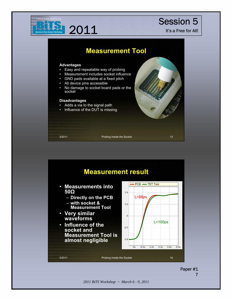
Measurement Tool
Advantages• Easy and repeatable way of probing• Measurement includes socket influence• GND pads available at a fixed pitch• All device pins accessible• No damage to socket board pads or the
socket
Disadvantages• Adds a via to the signal path • Influence of the DUT is missing
3/2011 Probing Inside the Socket 14
Measurement result
• Measurements into 50Ω– Directly on the PCB– with socket &
Measurement Tool • Very similar
waveforms• Influence of the
socket and Measurement Tool is almost negligible
tr=88ps
tr=100ps
It’s a Free for All!
Session 5
2011 BiTS Workshop ~ March 6 - 9, 2011
Paper #18
2011T W E L F T H A N N U A L
3/2011 Probing Inside the Socket 15
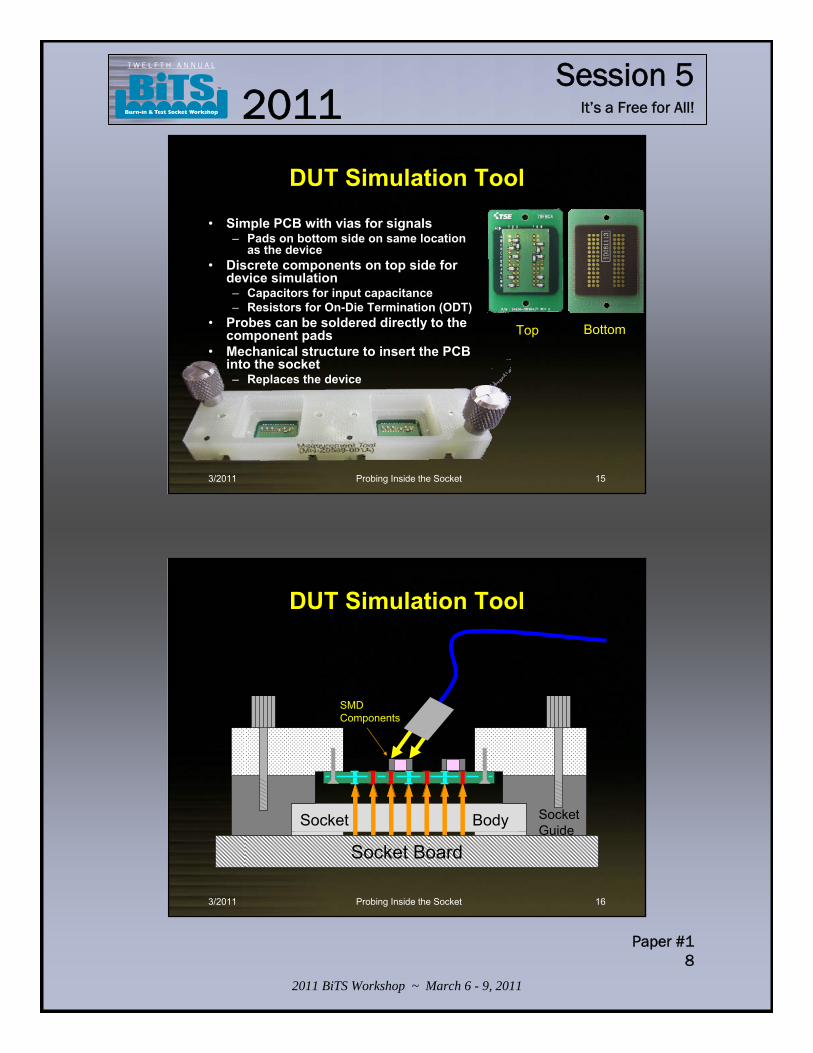
DUT Simulation Tool
• Simple PCB with vias for signals– Pads on bottom side on same location
as the device• Discrete components on top side for
device simulation– Capacitors for input capacitance– Resistors for On-Die Termination (ODT)
• Probes can be soldered directly to the component pads
• Mechanical structure to insert the PCB into the socket– Replaces the device
Top Bottom
3/2011 Probing Inside the Socket 16
DUT Simulation Tool
Socket Body SocketGuide
SMDComponents
Socket Board
It’s a Free for All!
Session 5
2011 BiTS Workshop ~ March 6 - 9, 2011
Paper #19
2011T W E L F T H A N N U A L
3/2011 Probing Inside the Socket 17
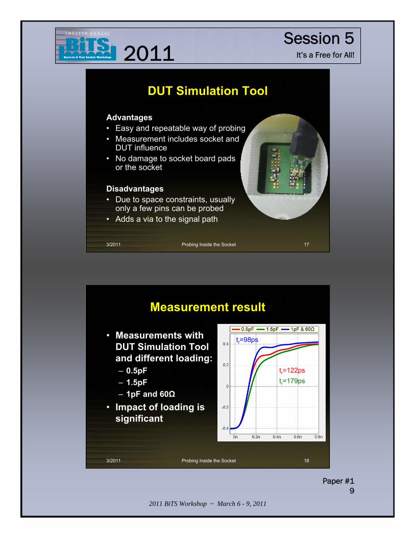
DUT Simulation Tool
Advantages• Easy and repeatable way of probing• Measurement includes socket and
DUT influence• No damage to socket board pads
or the socket
Disadvantages• Due to space constraints, usually
only a few pins can be probed• Adds a via to the signal path
3/2011 Probing Inside the Socket 18
Measurement result
• Measurements with DUT Simulation Tool and different loading:– 0.5pF– 1.5pF– 1pF and 60Ω
• Impact of loading is significant
tr=98ps
tr=179pstr=122ps
It’s a Free for All!
Session 5
2011 BiTS Workshop ~ March 6 - 9, 2011
Paper #110
2011T W E L F T H A N N U A L
3/2011 Probing Inside the Socket 19
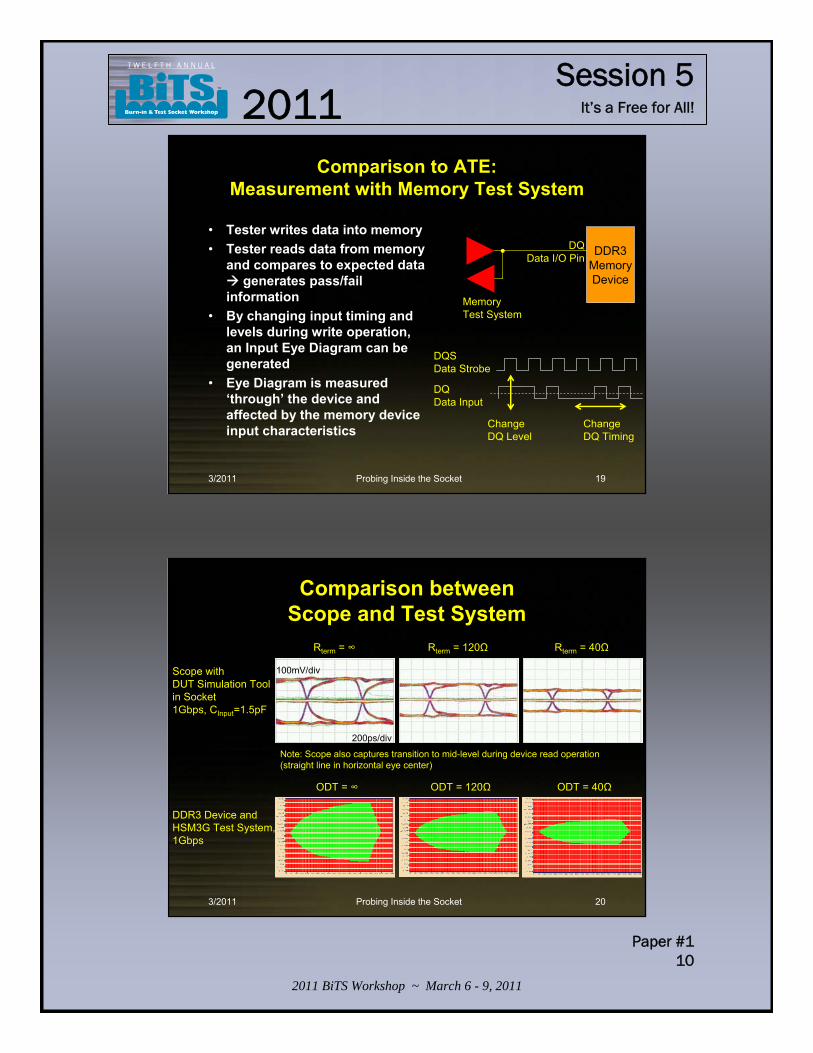
Comparison to ATE:Measurement with Memory Test System
DDR3MemoryDevice
DQData I/O Pin
MemoryTest System
• Tester writes data into memory• Tester reads data from memory
and compares to expected data generates pass/fail
information• By changing input timing and
levels during write operation, an Input Eye Diagram can be generated
• Eye Diagram is measured ‘through’ the device and affected by the memory device input characteristics
DQSData Strobe
DQData Input
ChangeDQ Timing
ChangeDQ Level
3/2011 Probing Inside the Socket 20
Comparison betweenScope and Test System
Scope withDUT Simulation Tool in Socket1Gbps, CInput=1.5pF
200ps/div
100mV/div
Rterm = ∞ Rterm = 120Ω Rterm = 40Ω
ODT = ∞ ODT = 120Ω ODT = 40Ω
DDR3 Device and HSM3G Test System, 1Gbps
Note: Scope also captures transition to mid-level during device read operation (straight line in horizontal eye center)

It’s a Free for All!
Session 5
2011 BiTS Workshop ~ March 6 - 9, 2011
Paper #111
2011T W E L F T H A N N U A L
3/2011 Probing Inside the Socket 21
Conclusion from Measurements
• The DUT input capacitance has a significant impact onto the signal shape and transition time
• A small, well-designed PCB with vias can be used to reliably probe signals inside the socket– the signal degradation caused by the PCB is
low– Discrete SMD components can be added to
represent the DUT input behavior• The Scope measurement using these
PCBs correlate well to ATE results
3/2011 Probing Inside the Socket 22
… so where is this approach useful?
• Characterizing sockets, e.g. for effects like cross-talk
• Performing measurements where the influence of the DUT cannot be neglected (e.g. if the bus is part of a tapped bus and the reflections of the DUT have significant impact)
• And, last but not least, make a customer happy when he requests to see the ‘real signal at the DUT’
It’s a Free for All!
Session 5
2011 BiTS Workshop ~ March 6 - 9, 2011
Paper #112
2011T W E L F T H A N N U A L
3/2011 Probing Inside the Socket 23
Acknowledgements
• Claus Pfander and Jose Moreira from Verigy HSM R&D, Germany
• Michael Daub from Verigy COE, Germany
• TSE Co., Ltd., Korea
It’s a Free for All!
Session 5
2011 BiTS Workshop ~ March 6 - 9, 2011
Paper #21
2011T W E L F T H A N N U A L
Conference Ready 1/25/11
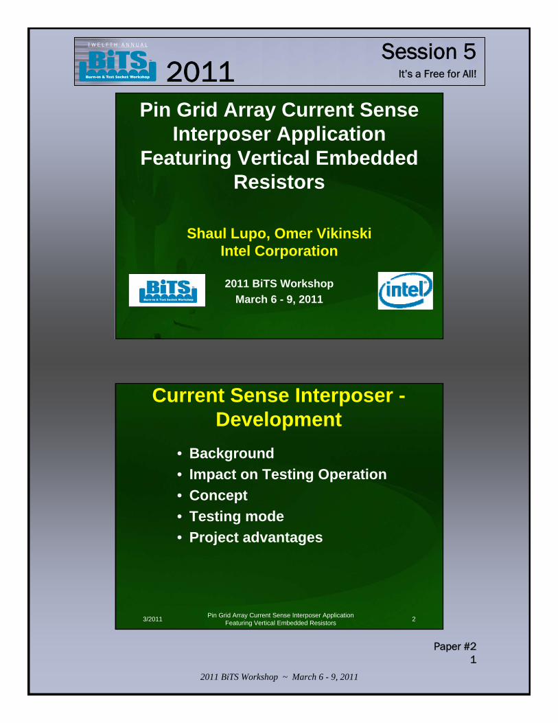
Pin Grid Array Current Sense Interposer Application
Featuring Vertical Embedded Resistors
2011 BiTS WorkshopMarch 6 - 9, 2011
Shaul Lupo, Omer VikinskiIntel Corporation
3/2011 Pin Grid Array Current Sense Interposer Application Featuring Vertical Embedded Resistors 2
Current Sense Interposer -Development
• Background• Impact on Testing Operation• Concept• Testing mode• Project advantages
It’s a Free for All!
Session 5
2011 BiTS Workshop ~ March 6 - 9, 2011
Paper #22
2011T W E L F T H A N N U A L
3/2011 Pin Grid Array Current Sense Interposer Application Featuring Vertical Embedded Resistors 3
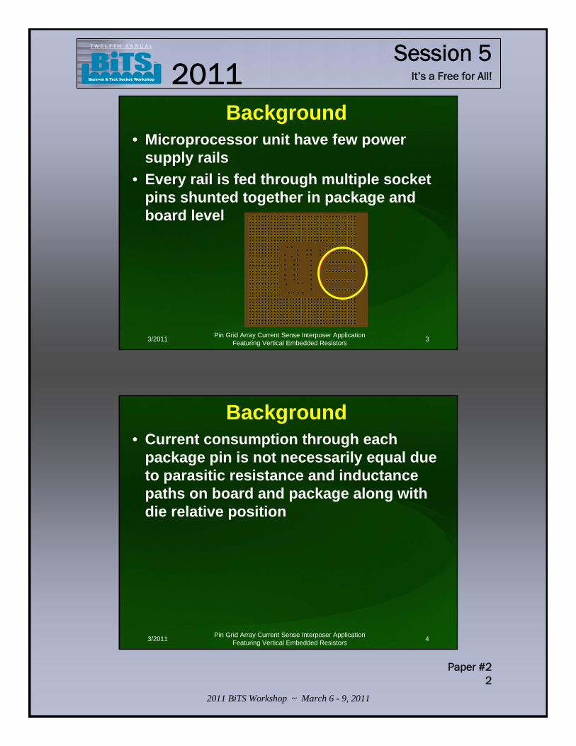
Background• Microprocessor unit have few power
supply rails• Every rail is fed through multiple socket
pins shunted together in package and board level
3/2011 Pin Grid Array Current Sense Interposer Application Featuring Vertical Embedded Resistors 4
Background• Current consumption through each
package pin is not necessarily equal due to parasitic resistance and inductance paths on board and package along with die relative position
It’s a Free for All!
Session 5
2011 BiTS Workshop ~ March 6 - 9, 2011
Paper #23
2011T W E L F T H A N N U A L
3/2011 Pin Grid Array Current Sense Interposer Application Featuring Vertical Embedded Resistors 5
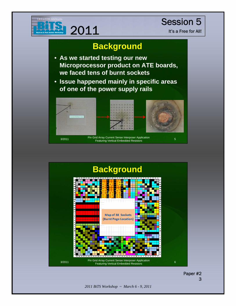
Background• As we started testing our new
Microprocessor product on ATE boards, we faced tens of burnt sockets
• Issue happened mainly in specific areas of one of the power supply rails
3/2011 Pin Grid Array Current Sense Interposer Application Featuring Vertical Embedded Resistors 6
Background
It’s a Free for All!
Session 5
2011 BiTS Workshop ~ March 6 - 9, 2011
Paper #24
2011T W E L F T H A N N U A L
3/2011 Pin Grid Array Current Sense Interposer Application Featuring Vertical Embedded Resistors 7
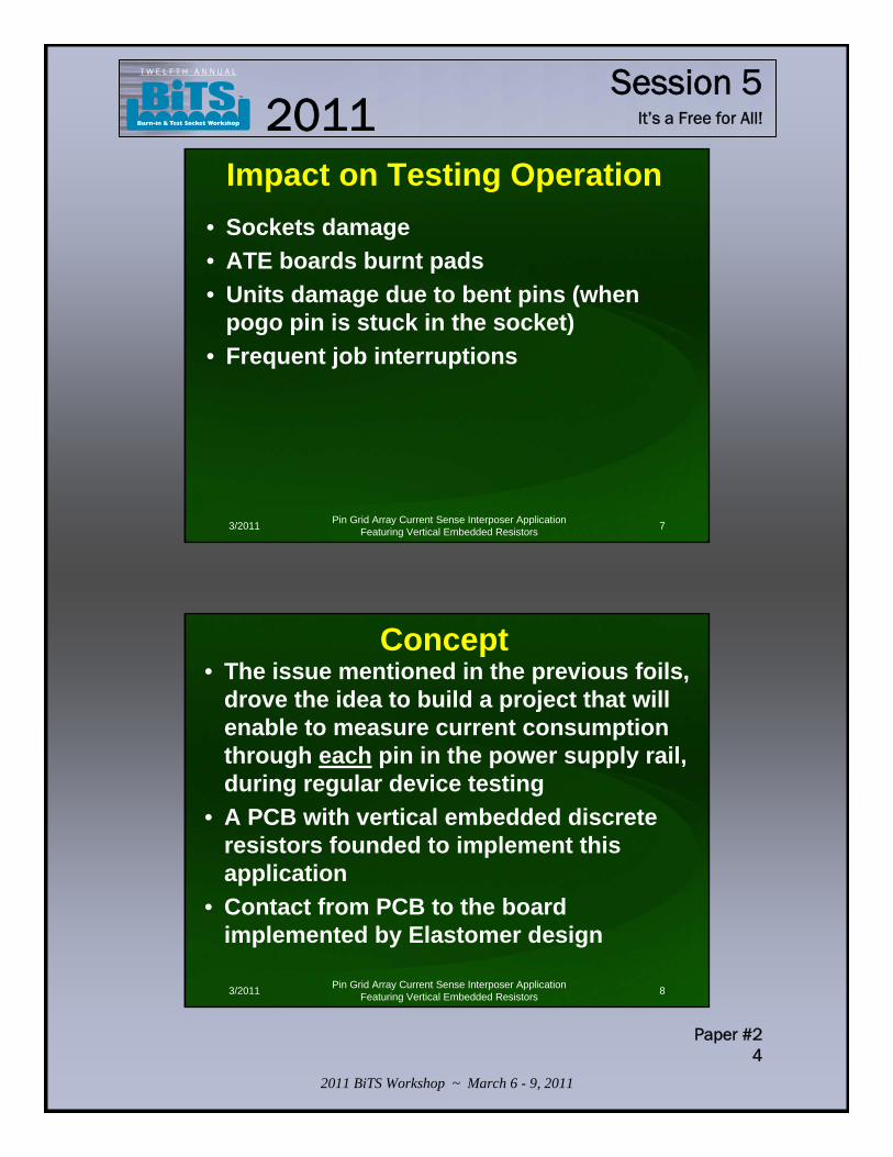
Impact on Testing Operation• Sockets damage• ATE boards burnt pads• Units damage due to bent pins (when
pogo pin is stuck in the socket)• Frequent job interruptions
3/2011 Pin Grid Array Current Sense Interposer Application Featuring Vertical Embedded Resistors 8
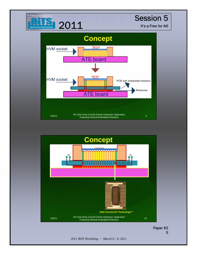
Concept• The issue mentioned in the previous foils,
drove the idea to build a project that will enable to measure current consumption through each pin in the power supply rail, during regular device testing
• A PCB with vertical embedded discrete resistors founded to implement this application
• Contact from PCB to the board implemented by Elastomer design
It’s a Free for All!
Session 5
2011 BiTS Workshop ~ March 6 - 9, 2011
Paper #25
2011T W E L F T H A N N U A L
3/2011 Pin Grid Array Current Sense Interposer Application Featuring Vertical Embedded Resistors 9
Concept
3/2011 Pin Grid Array Current Sense Interposer Application Featuring Vertical Embedded Resistors 10
Concept
R&D Circuits EC Technology™
It’s a Free for All!
Session 5
2011 BiTS Workshop ~ March 6 - 9, 2011
Paper #26
2011T W E L F T H A N N U A L
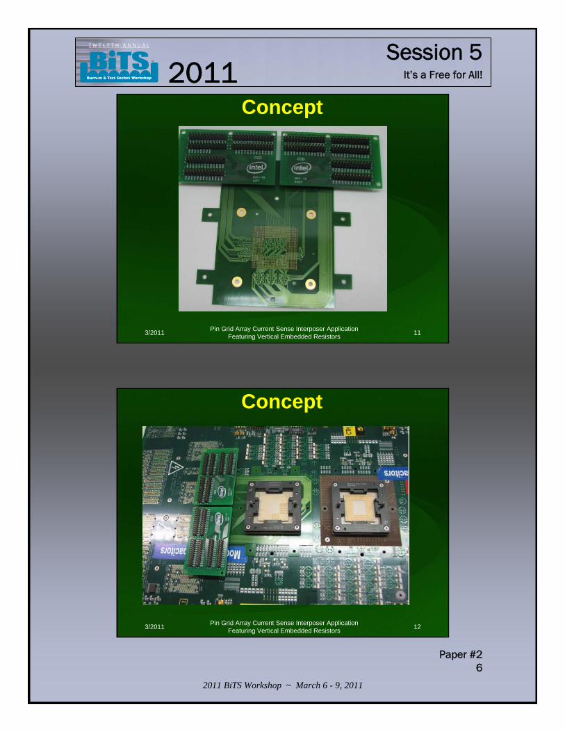
3/2011 Pin Grid Array Current Sense Interposer Application Featuring Vertical Embedded Resistors 11
Concept
3/2011 Pin Grid Array Current Sense Interposer Application Featuring Vertical Embedded Resistors 12
Concept
It’s a Free for All!
Session 5
2011 BiTS Workshop ~ March 6 - 9, 2011
Paper #27
2011T W E L F T H A N N U A L
3/2011 Pin Grid Array Current Sense Interposer Application Featuring Vertical Embedded Resistors 13
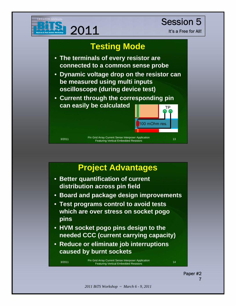
Testing Mode• The terminals of every resistor are
connected to a common sense probe • Dynamic voltage drop on the resistor can
be measured using multi inputs oscilloscope (during device test)
• Current through the corresponding pin can easily be calculated
3/2011 Pin Grid Array Current Sense Interposer Application Featuring Vertical Embedded Resistors 14
Project Advantages• Better quantification of current
distribution across pin field• Board and package design improvements • Test programs control to avoid tests
which are over stress on socket pogo pins
• HVM socket pogo pins design to the needed CCC (current carrying capacity)
• Reduce or eliminate job interruptions caused by burnt sockets
It’s a Free for All!
Session 5
2011 BiTS Workshop ~ March 6 - 9, 2011
Paper #31
2011T W E L F T H A N N U A L
Conference Ready 1/30/11
PCB Pad Wear Analysis at 0.4mm Pitch
- the story continues...
2011 BiTS WorkshopMarch 6- 9, 2011
Valts Treibergs & Chris CudaMultitest
PCB Pad Wear Analysis at 0.4mm Pitch 203/2011
• Recap of 2010 - .8mm pad wear highlights• .4mm pad construction• Experimental setup and method• Objectives of investigation• Results: Probe tip impact on .4mm pads• Results: 1.27µm vs 0.75µm gold• Results: Via-fill material impact on pad wear• Results: Alternative platings• Summary
Presentation Agenda
It’s a Free for All!
Session 5
2011 BiTS Workshop ~ March 6 - 9, 2011
Paper #32
2011T W E L F T H A N N U A L
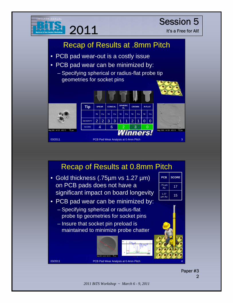
Recap of Results at .8mm Pitch• PCB pad wear-out is a costly issue• PCB pad wear can be minimized by:
– Specifying spherical or radius-flat probe tip geometries for socket pins
PCB Pad Wear Analysis at 0.4mm Pitch 303/2011
Tip SPEAR CONICAL SPHERICAL CROWN R-FLAT
Ni Cu Ni Cu Ni Cu Ni Cu Ni Cu
SEVERITY 2 2 3 3 1 1 2 1 0 0SCORE 4 6 2 3 0
Recap of Results at 0.8mm Pitch• Gold thickness (.75µm vs 1.27 µm)
on PCB pads does not have a significant impact on board longevity
• PCB pad wear can be minimized by:– Specifying spherical or radius-flat
probe tip geometries for socket pins– Insure that socket pin preload is
maintained to minimize probe chatter
PCB Pad Wear Analysis at 0.4mm Pitch 403/2011
Au 797,Cu 61, Ni 170
PCB SCORE
.75 µm Au 17
1.27 µm Au 15
It’s a Free for All!
Session 5
2011 BiTS Workshop ~ March 6 - 9, 2011
Paper #33
2011T W E L F T H A N N U A L
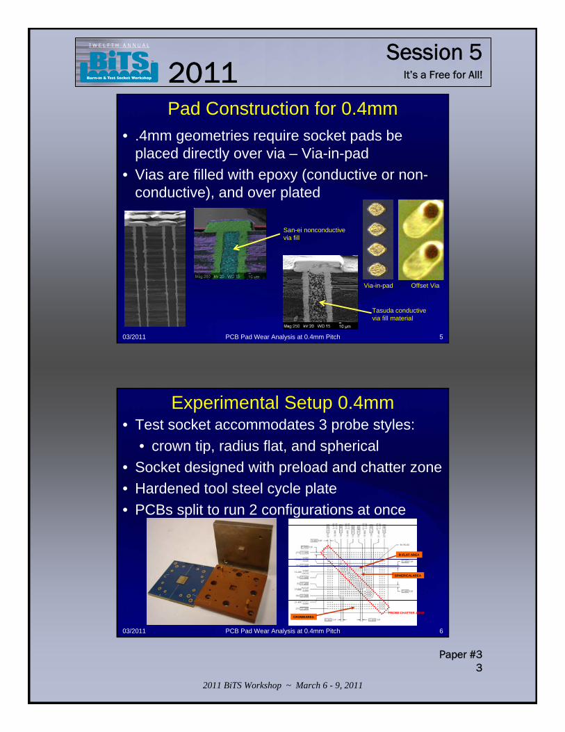
Pad Construction for 0.4mm• .4mm geometries require socket pads be
placed directly over via – Via-in-pad• Vias are filled with epoxy (conductive or non-
conductive), and over plated
PCB Pad Wear Analysis at 0.4mm Pitch 503/2011
Via-in-pad Offset Via
Tasuda conductive via fill material
San-ei nonconductive via fill
Experimental Setup 0.4mm
PCB Pad Wear Analysis at 0.4mm Pitch 603/2011
PROBE CHATTER ZONECROWNAREA
SPHERICALAREA
R-FLAT AREA
• Test socket accommodates 3 probe styles:• crown tip, radius flat, and spherical
• Socket designed with preload and chatter zone• Hardened tool steel cycle plate• PCBs split to run 2 configurations at once
It’s a Free for All!
Session 5
2011 BiTS Workshop ~ March 6 - 9, 2011
Paper #34
2011T W E L F T H A N N U A L
PCB Pad Wear Analysis at 0.4mm Pitch 703/2011
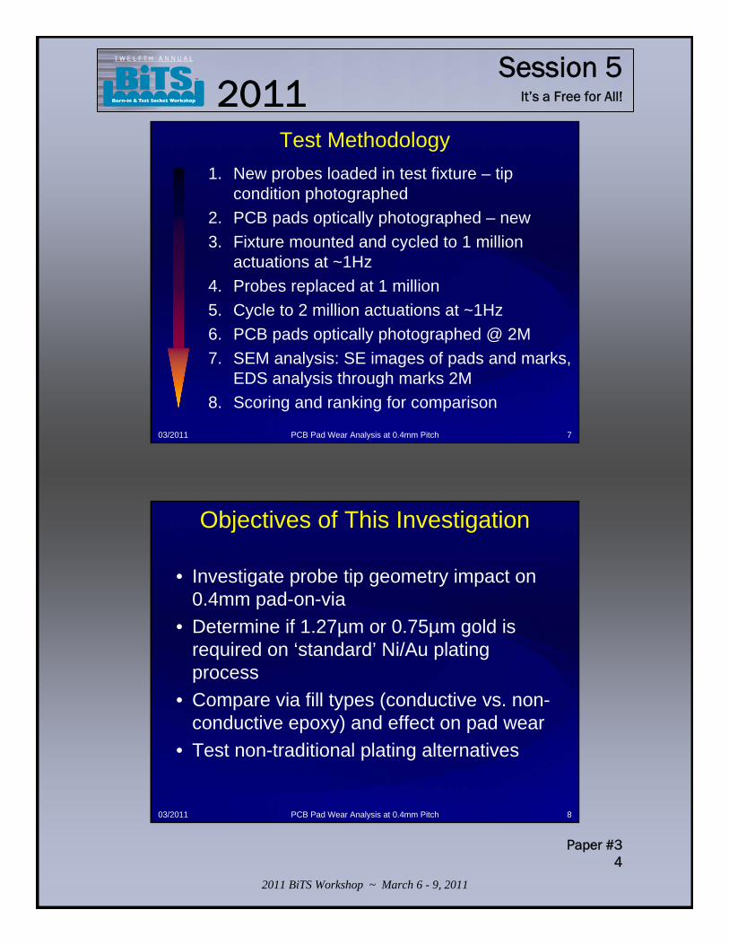
Test Methodology1. New probes loaded in test fixture – tip
condition photographed2. PCB pads optically photographed – new3. Fixture mounted and cycled to 1 million
actuations at ~1Hz4. Probes replaced at 1 million5. Cycle to 2 million actuations at ~1Hz6. PCB pads optically photographed @ 2M7. SEM analysis: SE images of pads and marks,
EDS analysis through marks 2M8. Scoring and ranking for comparison
Objectives of This Investigation
• Investigate probe tip geometry impact on 0.4mm pad-on-via
• Determine if 1.27µm or 0.75µm gold is required on ‘standard’ Ni/Au plating process
• Compare via fill types (conductive vs. non-conductive epoxy) and effect on pad wear
• Test non-traditional plating alternatives
PCB Pad Wear Analysis at 0.4mm Pitch 803/2011
It’s a Free for All!
Session 5
2011 BiTS Workshop ~ March 6 - 9, 2011
Paper #35
2011T W E L F T H A N N U A L
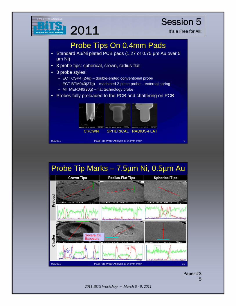
Probe Tips On 0.4mm Pads• Standard Au/Ni plated PCB pads (1.27 or 0.75 µm Au over 5
µm Ni)• 3 probe tips: spherical, crown, radius-flat• 3 probe styles:
– ECT CSP4 (24g) – double-ended conventional probe– ECT BTM040(37g) – machined 2-piece probe – external spring– MT MER040(30g) – flat technology probe
• Probes fully preloaded to the PCB and chattering on PCB
PCB Pad Wear Analysis at 0.4mm Pitch 903/2011
SPHERICALCROWN RADIUS-FLAT
Probe Tip Marks – 7.5µm Ni, 0.5µm Au
PCB Pad Wear Analysis at 0.4mm Pitch 1003/2011
Severe Cu Exposure
AuNi
Cu
It’s a Free for All!
Session 5
2011 BiTS Workshop ~ March 6 - 9, 2011
Paper #36
2011T W E L F T H A N N U A L
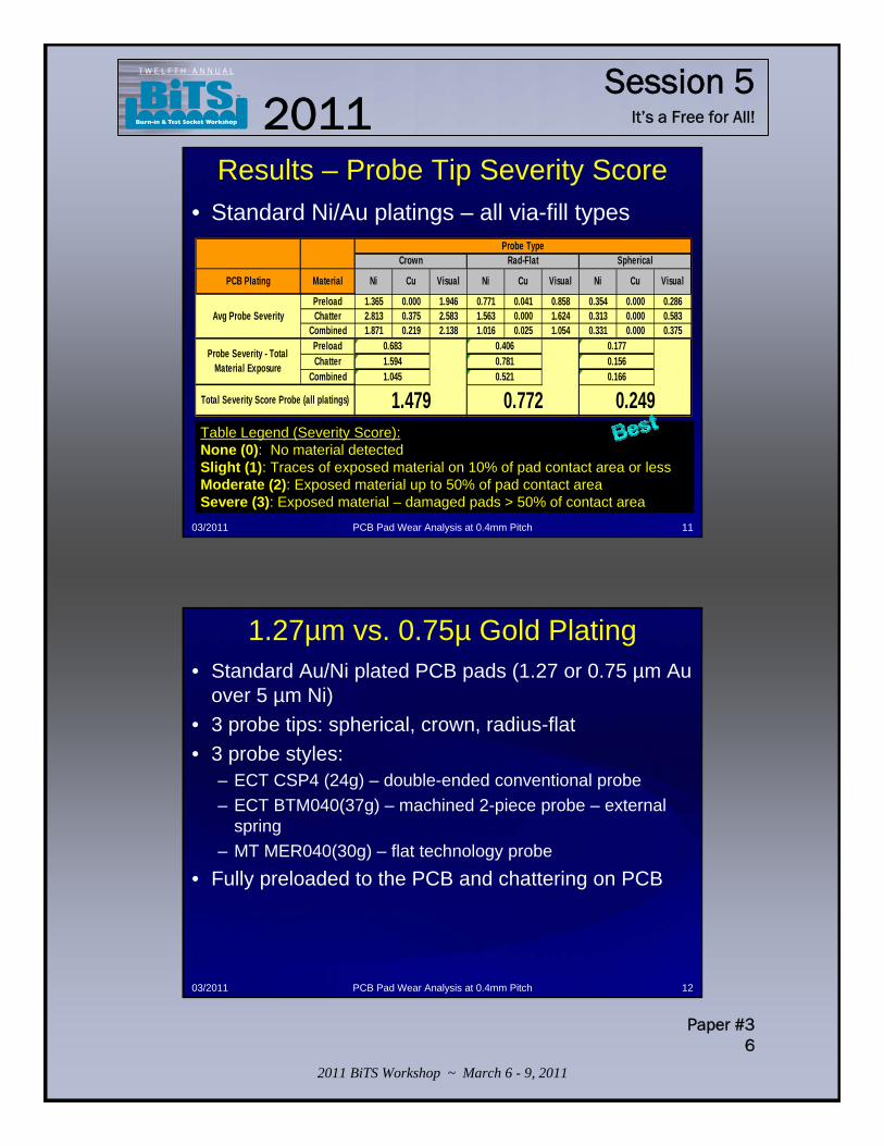
Results – Probe Tip Severity Score• Standard Ni/Au platings – all via-fill types
PCB Pad Wear Analysis at 0.4mm Pitch 1103/2011
PCB Plating Material Ni Cu Visual Ni Cu Visual Ni Cu Visual
Preload 1.365 0.000 1.946 0.771 0.041 0.858 0.354 0.000 0.286Chatter 2.813 0.375 2.583 1.563 0.000 1.624 0.313 0.000 0.583
Combined 1.871 0.219 2.138 1.016 0.025 1.054 0.331 0.000 0.375PreloadChatter
Combined
0.1771.594 0.781 0.1561.045 0.521 0.166
Total Severity Score Probe (all platings) 1.479 0.772 0.249
Avg Probe Severity
Probe Severity - Total Material Exposure
0.683 0.406
Probe TypeCrown Rad-Flat Spherical
Table Legend (Severity Score):None (0): No material detectedSlight (1): Traces of exposed material on 10% of pad contact area or lessModerate (2): Exposed material up to 50% of pad contact areaSevere (3): Exposed material – damaged pads > 50% of contact area
1.27µm vs. 0.75µ Gold Plating• Standard Au/Ni plated PCB pads (1.27 or 0.75 µm Au
over 5 µm Ni)• 3 probe tips: spherical, crown, radius-flat• 3 probe styles:
– ECT CSP4 (24g) – double-ended conventional probe– ECT BTM040(37g) – machined 2-piece probe – external
spring– MT MER040(30g) – flat technology probe
• Fully preloaded to the PCB and chattering on PCB
PCB Pad Wear Analysis at 0.4mm Pitch 1203/2011
It’s a Free for All!
Session 5
2011 BiTS Workshop ~ March 6 - 9, 2011
Paper #37
2011T W E L F T H A N N U A L
13
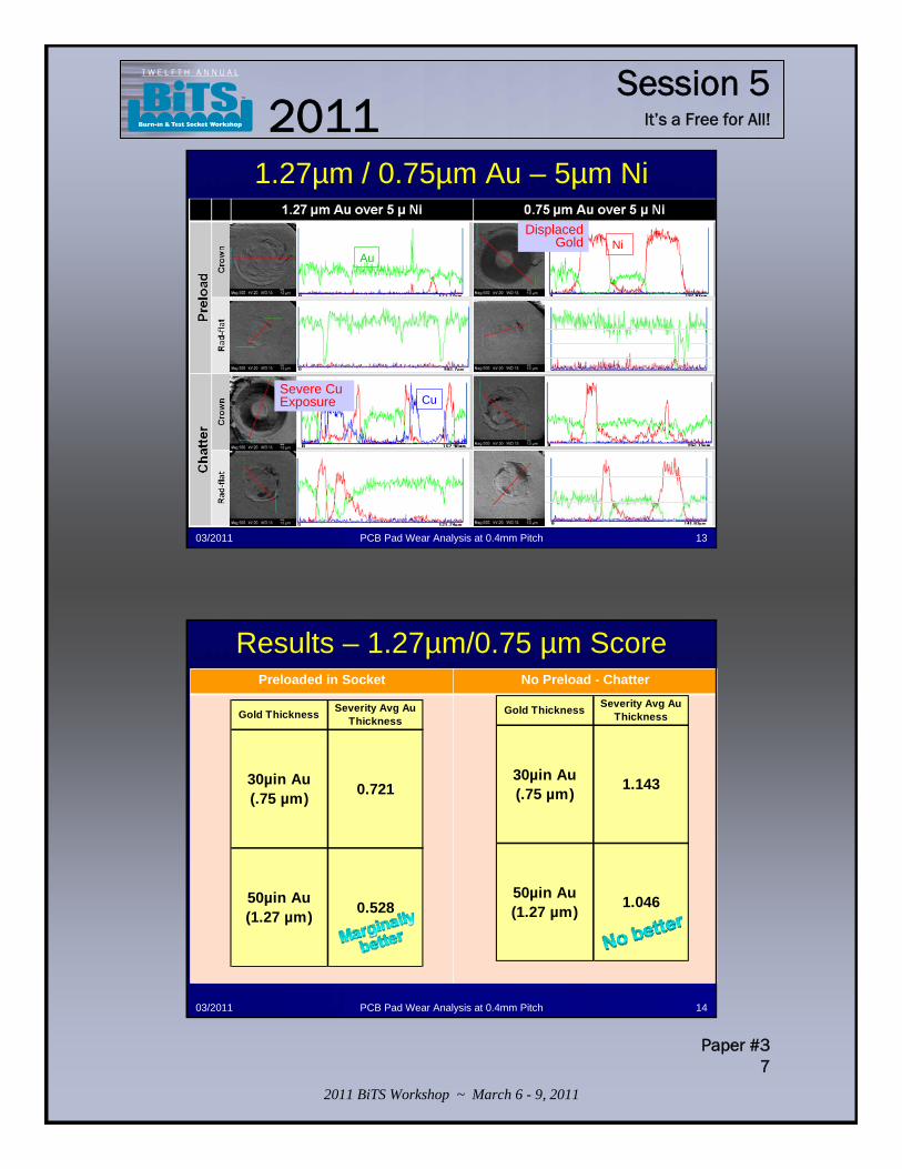
1.27µm / 0.75µm Au – 5µm Ni
PCB Pad Wear Analysis at 0.4mm Pitch03/2011
Severe Cu Exposure
Displaced Gold
AuNi
Cu
Results – 1.27µm/0.75 µm ScorePreloaded in Socket No Preload - Chatter
PCB Pad Wear Analysis at 0.4mm Pitch 1403/2011
50µin Au (1.27 µm) 1.046
Gold Thickness Severity Avg Au Thickness
30µin Au (.75 µm) 1.143
Gold Thickness
30µin Au (.75 µm)
50µin Au (1.27 µm)
Severity Avg Au Thickness
0.528
0.721
It’s a Free for All!
Session 5
2011 BiTS Workshop ~ March 6 - 9, 2011
Paper #38
2011T W E L F T H A N N U A L
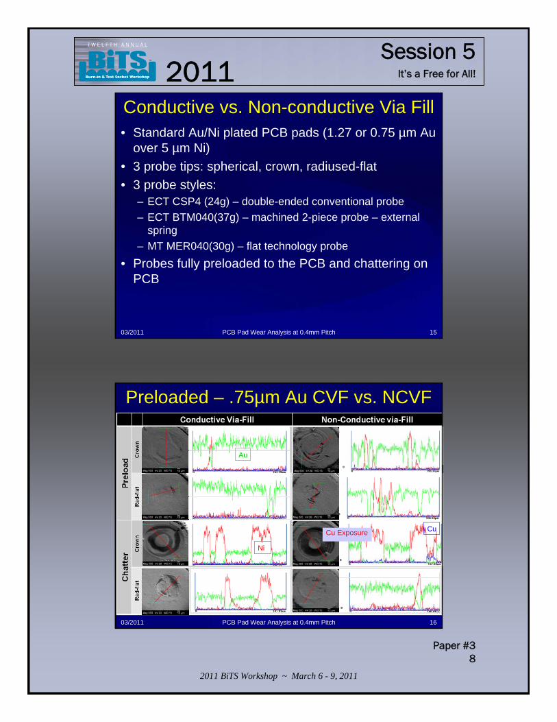
Conductive vs. Non-conductive Via Fill• Standard Au/Ni plated PCB pads (1.27 or 0.75 µm Au
over 5 µm Ni)• 3 probe tips: spherical, crown, radiused-flat• 3 probe styles:
– ECT CSP4 (24g) – double-ended conventional probe– ECT BTM040(37g) – machined 2-piece probe – external
spring– MT MER040(30g) – flat technology probe
• Probes fully preloaded to the PCB and chattering on PCB
PCB Pad Wear Analysis at 0.4mm Pitch 1503/2011
16
Preloaded – .75µm Au CVF vs. NCVF
PCB Pad Wear Analysis at 0.4mm Pitch03/2011
Cu Exposure
Au
Ni
Cu
It’s a Free for All!
Session 5
2011 BiTS Workshop ~ March 6 - 9, 2011
Paper #39
2011T W E L F T H A N N U A L
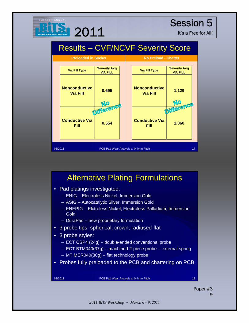
Results – CVF/NCVF Severity ScorePreloaded in Socket No Preload - Chatter
PCB Pad Wear Analysis at 0.4mm Pitch 1703/2011
Nonconductive Via Fill 1.129
Conductive Via Fill 1.060
Via Fill Type Severity Avg VIA FILLVia Fill Type
Nonconductive Via Fill
Conductive Via Fill
0.695
Severity Avg VIA FILL
0.554
Alternative Plating Formulations• Pad platings investigated:
– ENIG – Electroless Nickel, Immersion Gold– ASIG – Autocatalytic Silver, Immersion Gold– ENEPIG – Elctroless Nickel, Electroless Palladium, Immersion
Gold– DuraPad – new proprietary formulation
• 3 probe tips: spherical, crown, radiused-flat• 3 probe styles:
– ECT CSP4 (24g) – double-ended conventional probe– ECT BTM040(37g) – machined 2-piece probe – external spring– MT MER040(30g) – flat technology probe
• Probes fully preloaded to the PCB and chattering on PCB
PCB Pad Wear Analysis at 0.4mm Pitch 1803/2011
It’s a Free for All!
Session 5
2011 BiTS Workshop ~ March 6 - 9, 2011
Paper #310
2011T W E L F T H A N N U A L
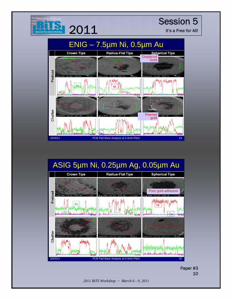
ENIG – 7.5µm Ni, 0.5µm Au
PCB Pad Wear Analysis at 0.4mm Pitch 1903/2011
Displaced Gold
Peenedgold
Au Ni
Cu
ASIG 5µm Ni, 0.25µm Ag, 0.05µm Au
PCB Pad Wear Analysis at 0.4mm Pitch 2003/2011
Poor gold adhesion
Au Ni
Cu

It’s a Free for All!
Session 5
2011 BiTS Workshop ~ March 6 - 9, 2011
Paper #311
2011T W E L F T H A N N U A L
ENEPIG – 7.5 µm Ni, .13µm Pd, 0.05µAu
PCB Pad Wear Analysis at 0.4mm Pitch 2103/2011
AuNi
Cu
Pd
DuraPad
PCB Pad Wear Analysis at 0.4mm Pitch 2203/2011
Au

It’s a Free for All!
Session 5
2011 BiTS Workshop ~ March 6 - 9, 2011
Paper #312
2011T W E L F T H A N N U A L
Alternative Plating Severity
PCB Pad Wear Analysis at 0.4mm Pitch 2303/2011
Alternative Plating SeverityPCB PlatingCOMBINED SEVERITY CHATTER
ENIG 7.5µNi/0.5µAu NCVF 1.500
DURAPAD NCVF 1.167
ASIG 5µNi,.25µAg,.05µAu NCVF 1.370
DURAPAD CVF 0.703
DURAPAD NCVF 0.370
ENIG 7.5µNi/0.5µAu CVF 2.649
ENEPIG 7.5µNi,.13µPd,.05µAu NCVF 1.278
ENIG 7.5µNi/0.5µAu NCVF 1.741
COMBINED SEVERITY PRELOAD
ALL SEVERITY
0.698
0.370
2.469
0.701
0.370
2.559
1.052 1.165
1.556 1.648
1.594 1.547
1.054 1.111
1.497 1.433
PCB Pad Wear Analysis at 0.4mm Pitch 2403/2011
Summing It All Up16 PCBs were cycled to 2M insertions each – 200 EDS analyses and
1000+ SEM/optical images were taken over the course of 1 year
•PCB pad wear can be minimized by:– Specifying spherical or radius-flat probe tip geometries for socket pins– Insure that socket pin preload is maintained to minimize probe chatter
•There is no significant difference in PCB pad wear whether vias filled with conductive or non-conductive filler•1.27µm Au offers no significant advantage for pad life compared to 0.75µm•Alternate plating formulations used in other electronic applications do not perform better than standard Ni/Au, however, DuraPad shows interesting results and merits further study
It’s a Free for All!
Session 5
2011 BiTS Workshop ~ March 6 - 9, 2011
Paper #41
2011T W E L F T H A N N U A L
Conference Ready 2/1/11
Thermal Testing – some tidbits from the lab
2011 BiTS WorkshopMarch 6 - 9, 2011
James Forster+ and John Moore* + WELLS-CTI *Texas Instruments
3/2011 Thermal Testing – some tidbits from the lab 2
Agenda
• Introduction and background• Review of past BiTS• The language of thermal testing• So what and who cares?• Experimental issues and difficulties• Closing comments
It’s a Free for All!
Session 5
2011 BiTS Workshop ~ March 6 - 9, 2011
Paper #42
2011T W E L F T H A N N U A L
3/2011 Thermal Testing – some tidbits from the lab 3
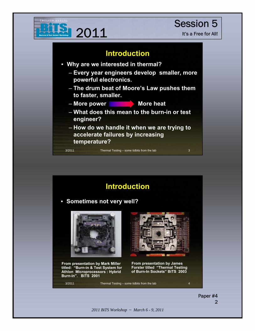
Introduction• Why are we interested in thermal?
– Every year engineers develop smaller, more powerful electronics.
– The drum beat of Moore’s Law pushes them to faster, smaller.
– More power More heat– What does this mean to the burn-in or test
engineer? – How do we handle it when we are trying to
accelerate failures by increasing temperature?
3/2011 Thermal Testing – some tidbits from the lab 4
Introduction
• Sometimes not very well?
From presentation by James Forster titled “Thermal Testing of Burn-In Sockets” BiTS 2003
From presentation by Mark Miller titled: “Burn-in & Test System for Athlon Microprocessors : Hybrid Burn-in”. BiTS 2001
It’s a Free for All!
Session 5
2011 BiTS Workshop ~ March 6 - 9, 2011
Paper #43
2011T W E L F T H A N N U A L
3/2011 Thermal Testing – some tidbits from the lab 5
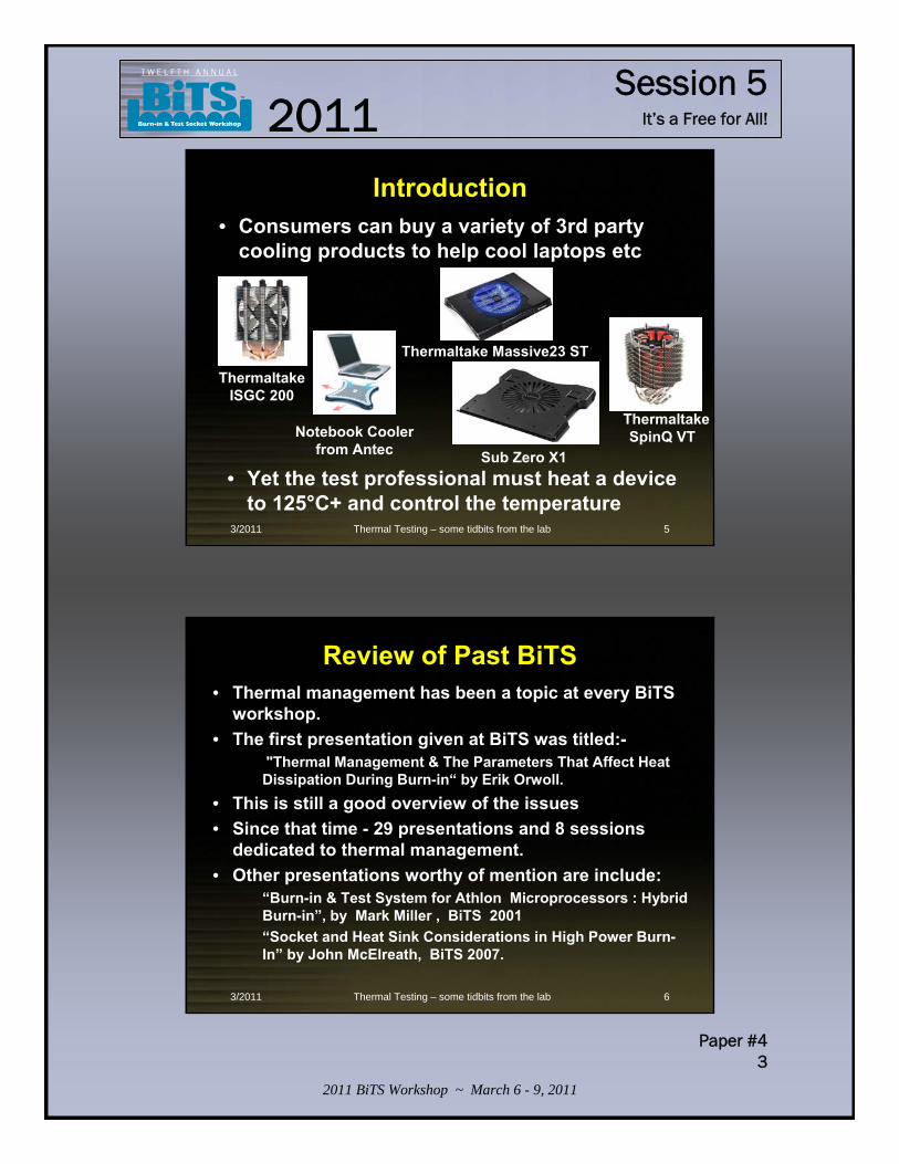
Introduction• Consumers can buy a variety of 3rd party
cooling products to help cool laptops etc
Notebook Cooler from Antec
• Yet the test professional must heat a device to 125°C+ and control the temperature
Sub Zero X1
Thermaltake Massive23 ST
ThermaltakeSpinQ VT
ThermaltakeISGC 200
3/2011 Thermal Testing – some tidbits from the lab 6
Review of Past BiTS• Thermal management has been a topic at every BiTS
workshop.• The first presentation given at BiTS was titled:-
"Thermal Management & The Parameters That Affect Heat Dissipation During Burn-in“ by Erik Orwoll.
• This is still a good overview of the issues• Since that time - 29 presentations and 8 sessions
dedicated to thermal management.• Other presentations worthy of mention are include:
“Burn-in & Test System for Athlon Microprocessors : Hybrid Burn-in”, by Mark Miller , BiTS 2001“Socket and Heat Sink Considerations in High Power Burn-In” by John McElreath, BiTS 2007.
It’s a Free for All!
Session 5
2011 BiTS Workshop ~ March 6 - 9, 2011
Paper #44
2011T W E L F T H A N N U A L
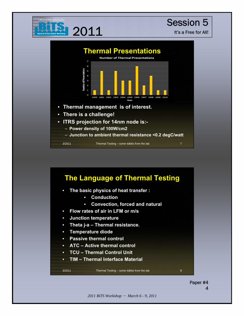
3/2011 Thermal Testing – some tidbits from the lab 7
Thermal Presentations
• Thermal management is of interest.• There is a challenge!• ITRS projection for 14nm node is:-
– Power density of 100W/cm2– Junction to ambient thermal resistance <0.2 degC/watt
3/2011 Thermal Testing – some tidbits from the lab 8
The Language of Thermal Testing • The basic physics of heat transfer :
• Conduction• Convection, forced and natural
• Flow rates of air in LFM or m/s• Junction temperature• Theta j-a – Thermal resistance. • Temperature diode• Passive thermal control• ATC – Active thermal control• TCU – Thermal Control Unit• TIM – Thermal Interface Material
It’s a Free for All!
Session 5
2011 BiTS Workshop ~ March 6 - 9, 2011
Paper #45
2011T W E L F T H A N N U A L
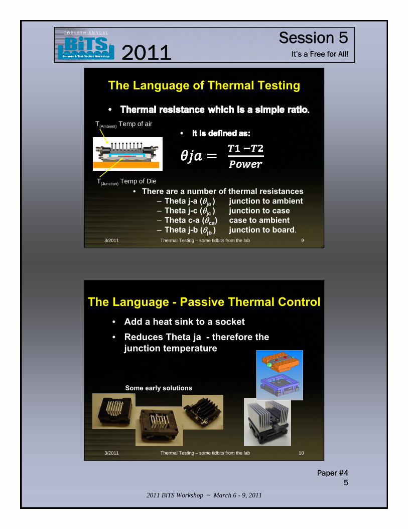
3/2011 Thermal Testing – some tidbits from the lab 9
The Language of Thermal Testing
T(Junction) Temp of Die
T(Ambient) Temp of air
• There are a number of thermal resistances– Theta j-a (θja ) junction to ambient– Theta j-c (θjc ) junction to case– Theta c-a (θca) case to ambient– Theta j-b (θjb ) junction to board.
3/2011 Thermal Testing – some tidbits from the lab 10
The Language - Passive Thermal Control• Add a heat sink to a socket• Reduces Theta ja - therefore the
junction temperature
Some early solutions
It’s a Free for All!
Session 5
2011 BiTS Workshop ~ March 6 - 9, 2011
Paper #46
2011T W E L F T H A N N U A L
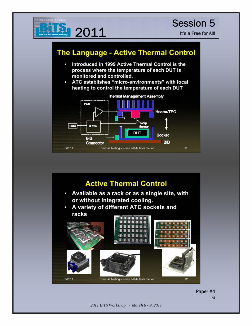
3/2011 Thermal Testing – some tidbits from the lab 11
The Language - Active Thermal Control• Introduced in 1999 Active Thermal Control is the
process where the temperature of each DUT is monitored and controlled.
• ATC establishes “micro-environments” with local heating to control the temperature of each DUT
3/2011 Thermal Testing – some tidbits from the lab 12
Active Thermal Control• Available as a rack or as a single site, with
or without integrated cooling.• A variety of different ATC sockets and
racks
It’s a Free for All!
Session 5
2011 BiTS Workshop ~ March 6 - 9, 2011
Paper #47
2011T W E L F T H A N N U A L
3/2011 Thermal Testing – some tidbits from the lab 13
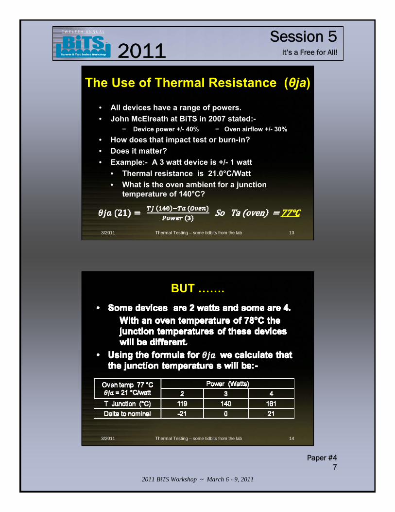
The Use of Thermal Resistance (θja)
• All devices have a range of powers.• John McElreath at BiTS in 2007 stated:-
− Device power +/- 40% − Oven airflow +/- 30%• How does that impact test or burn-in?• Does it matter?• Example:- A 3 watt device is +/- 1 watt
• Thermal resistance is 21.0°C/Watt• What is the oven ambient for a junction
temperature of 140°C?
3/2011 Thermal Testing – some tidbits from the lab 14
BUT …….
It’s a Free for All!
Session 5
2011 BiTS Workshop ~ March 6 - 9, 2011
Paper #48
2011T W E L F T H A N N U A L
3/2011 Thermal Testing – some tidbits from the lab 15
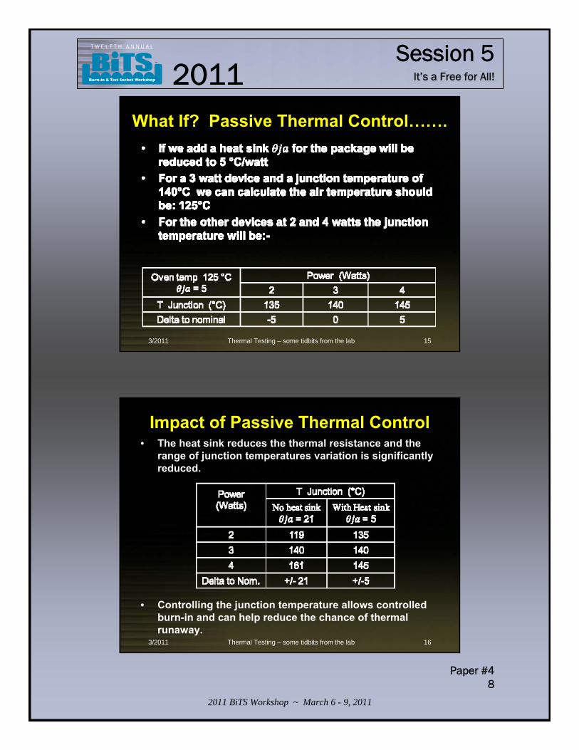
What If? Passive Thermal Control…….
3/2011 Thermal Testing – some tidbits from the lab 16
Impact of Passive Thermal Control • The heat sink reduces the thermal resistance and the
range of junction temperatures variation is significantly reduced.
• Controlling the junction temperature allows controlled burn-in and can help reduce the chance of thermal runaway.
It’s a Free for All!
Session 5
2011 BiTS Workshop ~ March 6 - 9, 2011
Paper #49
2011T W E L F T H A N N U A L
3/2011 Thermal Testing – some tidbits from the lab 17
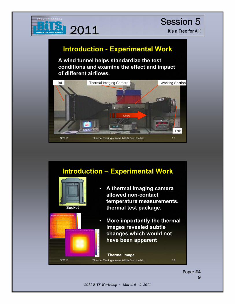
Introduction - Experimental WorkA wind tunnel helps standardize the test conditions and examine the effect and impact of different airflows.
Working Section Inlet Thermal Imaging Camera
Airflow
Exit
3/2011 Thermal Testing – some tidbits from the lab 18
Introduction – Experimental Work
• A thermal imaging camera allowed non-contact temperature measurements. thermal test package.
• More importantly the thermal images revealed subtle changes which would not have been apparent
Socket
Thermal image
It’s a Free for All!
Session 5
2011 BiTS Workshop ~ March 6 - 9, 2011
Paper #410
2011T W E L F T H A N N U A L
3/2011 Thermal Testing – some tidbits from the lab 19
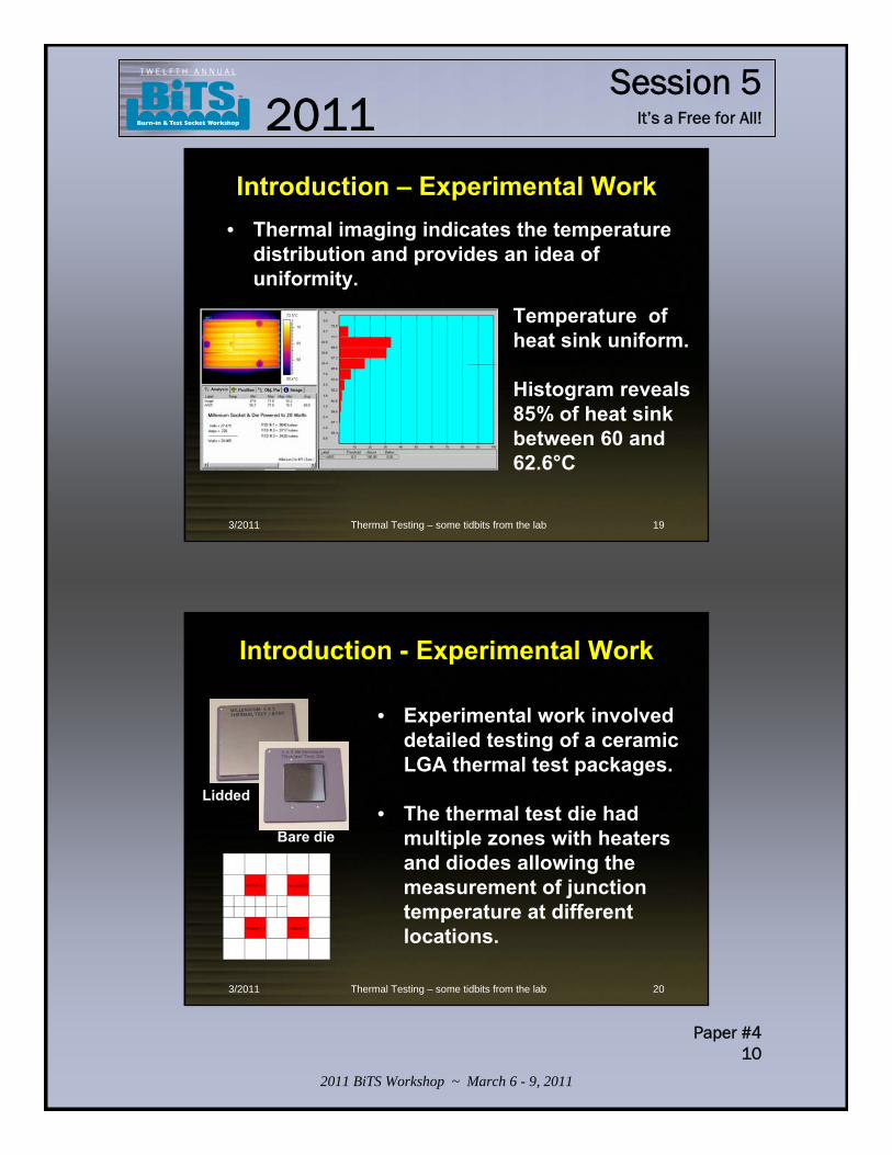
Introduction – Experimental Work• Thermal imaging indicates the temperature
distribution and provides an idea of uniformity.
Temperature of heat sink uniform.
Histogram reveals 85% of heat sink between 60 and 62.6°C
3/2011 Thermal Testing – some tidbits from the lab 20
Introduction - Experimental Work
• Experimental work involved detailed testing of a ceramic LGA thermal test packages.
• The thermal test die had multiple zones with heaters and diodes allowing the measurement of junction temperature at different locations.
Lidded
Bare die
It’s a Free for All!
Session 5
2011 BiTS Workshop ~ March 6 - 9, 2011
Paper #411
2011T W E L F T H A N N U A L
3/2011 Thermal Testing – some tidbits from the lab 21
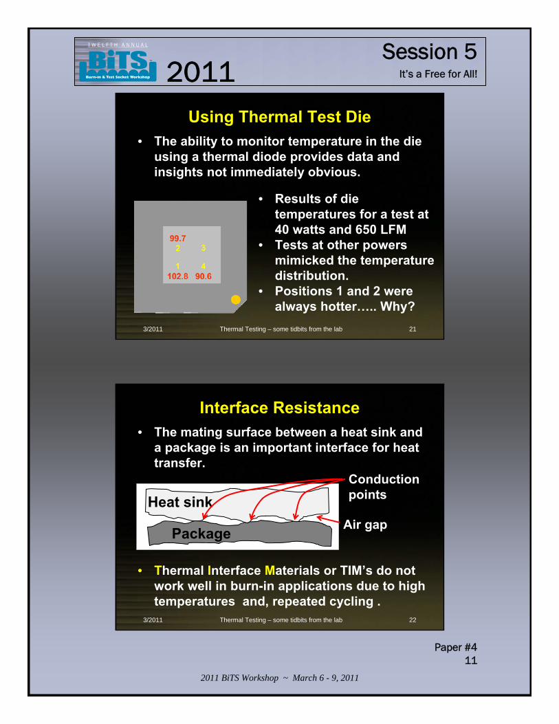
Using Thermal Test Die• The ability to monitor temperature in the die
using a thermal diode provides data and insights not immediately obvious.
• Results of die temperatures for a test at 40 watts and 650 LFM
• Tests at other powers mimicked the temperature distribution.
• Positions 1 and 2 were always hotter….. Why?
3/2011 Thermal Testing – some tidbits from the lab 22
Interface Resistance• The mating surface between a heat sink and
a package is an important interface for heat transfer.
• Thermal Interface Materials or TIM’s do not work well in burn-in applications due to high temperatures and, repeated cycling .
Heat sink
Package
Conduction points
Air gap
It’s a Free for All!
Session 5
2011 BiTS Workshop ~ March 6 - 9, 2011
Paper #412
2011T W E L F T H A N N U A L
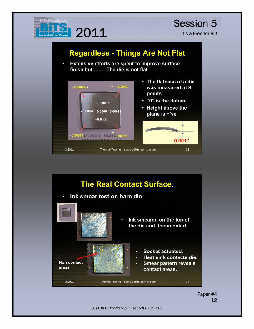
3/2011 Thermal Testing – some tidbits from the lab 23
Regardless - Things Are Not Flat• Extensive efforts are spent to improve surface
finish but …… The die is not flat
• The flatness of a die was measured at 9 points
• “0” is the datum.• Height above the
plane is +’ve
0.001”
3/2011 Thermal Testing – some tidbits from the lab 24
• Ink smear test on bare die
• Ink smeared on the top of the die and documented
• Socket actuated. • Heat sink contacts die.• Smear pattern reveals
contact areas.Non contact areas
The Real Contact Surface.
It’s a Free for All!
Session 5
2011 BiTS Workshop ~ March 6 - 9, 2011
Paper #413
2011T W E L F T H A N N U A L
3/2011 Thermal Testing – some tidbits from the lab 25
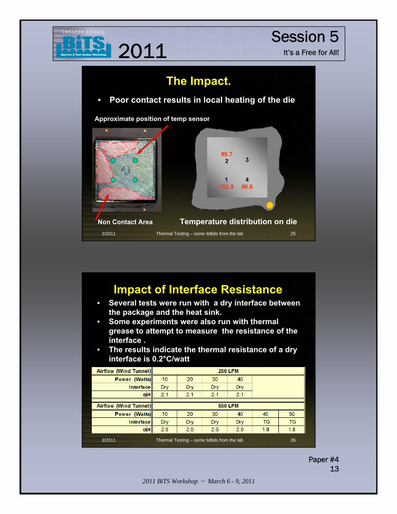
• Poor contact results in local heating of the die
The Impact.
Non Contact Area Temperature distribution on die
Approximate position of temp sensor
3/2011 Thermal Testing – some tidbits from the lab 26
Impact of Interface Resistance• Several tests were run with a dry interface between
the package and the heat sink.• Some experiments were also run with thermal
grease to attempt to measure the resistance of the interface .
• The results indicate the thermal resistance of a dry interface is 0.2°C/watt
It’s a Free for All!
Session 5
2011 BiTS Workshop ~ March 6 - 9, 2011
Paper #414
2011T W E L F T H A N N U A L
3/2011 Thermal Testing – some tidbits from the lab 27
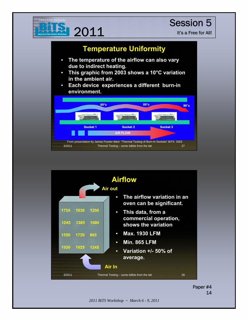
Temperature Uniformity• The temperature of the airflow can also vary
due to indirect heating. • This graphic from 2003 shows a 10°C variation
in the ambient air.• Each device experiences a different burn-in
environment.
From presentation by James Forster titled “Thermal Testing of Burn-In Sockets” BiTS 2003
3/2011 Thermal Testing – some tidbits from the lab 28
• The airflow variation in an oven can be significant.
• This data, from a commercial operation, shows the variation
• Max. 1930 LFM• Min. 865 LFM• Variation +/- 50% of
average.
Airflow
Air In
1755 1830 1200
1245 1385 1000
1930 1825 1245
1550 1720 865
Air out
It’s a Free for All!
Session 5
2011 BiTS Workshop ~ March 6 - 9, 2011
Paper #415
2011T W E L F T H A N N U A L
3/2011 Thermal Testing – some tidbits from the lab 29
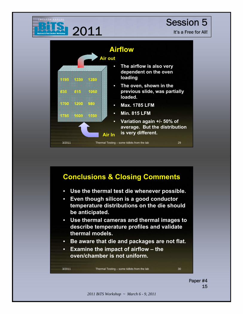
• The airflow is also very dependent on the oven loading
• The oven, shown in the previous slide, was partially loaded.
• Max. 1785 LFM• Min. 815 LFM• Variation again +/- 50% of
average. But the distribution is very different.
Airflow
Air In
1195 1330 1260
835 815 1060
1785 1600 1550
1700 1200 980
Air out
3/2011 Thermal Testing – some tidbits from the lab 30
Conclusions & Closing Comments
• Use the thermal test die whenever possible.• Even though silicon is a good conductor
temperature distributions on the die should be anticipated.
• Use thermal cameras and thermal images to describe temperature profiles and validate thermal models.
• Be aware that die and packages are not flat.• Examine the impact of airflow – the
oven/chamber is not uniform.
It’s a Free for All!
Session 5
2011 BiTS Workshop ~ March 6 - 9, 2011
Paper #416
2011T W E L F T H A N N U A L
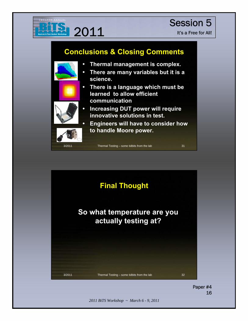
3/2011 Thermal Testing – some tidbits from the lab 31
Conclusions & Closing Comments• Thermal management is complex.• There are many variables but it is a
science.• There is a language which must be
learned to allow efficient communication
• Increasing DUT power will require innovative solutions in test.
• Engineers will have to consider how to handle Moore power.
3/2011 Thermal Testing – some tidbits from the lab 32
Final Thought
So what temperature are you actually testing at?