arm on-chip sram and/or rom 32-bit data...
TRANSCRIPT

Rev. 1354B–07/00
AT91ARM® Thumb®
Microcontrollers
AT91M40800AT91R40807AT91M40807
Features• Incorporates the ARM7TDMI™ ARM® Thumb® Processor Core
– High-performance 32-bit RISC Architecture– High-density 16-bit Instruction Set – Leader in MIPS/Watt– Embedded ICE (In-Circuit Emulation)
• On-chip SRAM and/or ROM– 32-bit Data Bus– Single-clock Cycle Access
• Fully Programmable External Bus Interface (EBI)– Maximum External Address Space of 64M Bytes– Up to 8 Chip Selects– Software Programmable 8/16-bit External Databus
• 8-level Priority, Individually Maskable, Vectored Interrupt Controller– 4 External Interrupts, Including a High-priority Low-latency Interrupt Request
• 32 Programmable I/O Lines• 3-channel 16-bit Timer/Counter
– 3 External Clock Inputs– 2 Multi-purpose I/O Pins per Channel
• 2 USARTs– 2 Dedicated Peripheral Data Controller (PDC) Channels per USART
• Programmable Watchdog Timer • Advanced Power-saving Features
– CPU and Peripheral Can be Deactivated Individually• Fully Static Operation:
– 0 Hz to 16 MHz at 1.8V– 0 Hz to 33 MHz at 2.7V– 0 Hz to 40 MHz at 3.0V
• 1.8V to 3.6V Operating Range• Available in a 100-lead TQFP Package
DescriptionThe AT91X40 Series is a member of the Atmel AT91 16/32-bit Microcontroller family,which is based on the ARM7TDMI processor core. This processor has a high-perfor-mance 32-bit RISC architecture with a high-density 16-bit instruction set and very lowpower consumption. In addition, a large number of internally banked registers result invery fast exception handling, making the device ideal for real-time controlapplications.
The AT91X40 Series features a direct connection to off-chip memory, including Flash,through the fully programmable External Bus Interface (EBI). An eight-level priorityvectored interrupt controller, in conjunction with the Peripheral Data Controller signifi-cantly improve the real-time performance of the device.
The device is manufactured using Atmel’s high-density CMOS technology. By com-bining the ARM7TDMI processor core with on-chip high-speed memory and a widerange of peripheral functions on a monolithic chip, the Atmel AT91X40 Series is apowerful microcontroller that offers a flexible, cost-effective solution to many compute-intensive embedded control applications.
Microcontroller SRAM Extended SRAM ROM
AT91M40800 8K Byte – –
AT91R40807 8K Byte 128K Byte –
AT91M40807 8K Byte – 128K Byte
1

Pin ConfigurationFigure 1. AT91X40 Series Pinout (Top View)
P21
/TX
D1/
NT
RI
P20
/SC
K1
P19
P18
P17
P16
P15
/RX
D0
P14
/TX
D0
P13
/SC
K0
P12
/FIQ
GN
D
P11
/IRQ
2
P10
/IRQ
1
VD
D
VD
D
P9/
IRQ
0
P8/
TIO
B2
P7/
TIO
A2
P6/
TC
LK2
P5/
TIO
B1
P4/
TIO
A1
P3/
TC
LK1
GN
D
GN
D
P2/
TIO
B0
P1/TIOA0
P0/TCLK0
D15
D14
D13
D12
VDD
D11
D10
D9
D8
D7
D6
D5
GND
D4
D3
D2
D1
D0
P31/A23/CS4
P30/A22/CS5
VDD
VDD
P29/A21/CS6
P22/RXD1
NWR1/NUB
GND
NRST
NWDOVF
VDD
MCKI
P23
P24/BMS
P25/MCKO
GND
GND
TMS
TDO
TCK
NRD/NOE
NWR0/NWE
VDD
VDD
NWAIT
NCS0
NCS1
P26/NCS2
P27/NCS3
A0/
NLB A
1
A2
A2
A3
A4
A5
A6
A7
VD
D A8
A9
A10
A11
A12
A13
A14
GN
D
GN
D
A15
A16
A17
A18
A19
P28
/A20
/CS
7
GN
D
1 25
100-lead TQFP
2 3 4 5 6 7 8 9 10 11 12 13 14 15 116 17 18 19 20 21 22 23 24
26
50
27
28
29
30
31
32
33
34
35
36
37
38
39
40
41
42
43
44
45
46
47
48
49
75 5174 73 72 71 70 69 68 67 66 65 64 63 62 61 60 59 58 57 56 55 54 53 52
100
76
99
98
97
96
95
94
93
92
91
90
89
88
87
86
85
84
83
82
81
80
79
78
77
TDI
AT91X40 Series2
AT91X40 Series
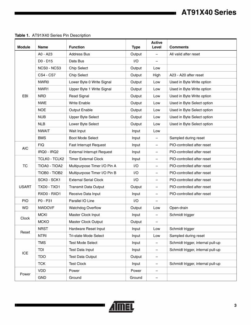
Table 1. AT91X40 Series Pin Description
Module Name Function TypeActive Level Comments
EBI
A0 - A23 Address Bus Output – All valid after reset
D0 - D15 Data Bus I/O –
NCS0 - NCS3 Chip Select Output Low
CS4 - CS7 Chip Select Output High A23 - A20 after reset
NWR0 Lower Byte 0 Write Signal Output Low Used in Byte Write option
NWR1 Upper Byte 1 Write Signal Output Low Used in Byte Write option
NRD Read Signal Output Low Used in Byte Write option
NWE Write Enable Output Low Used in Byte Select option
NOE Output Enable Output Low Used in Byte Select option
NUB Upper Byte Select Output Low Used in Byte Select option
NLB Lower Byte Select Output Low Used in Byte Select option
NWAIT Wait Input Input Low
BMS Boot Mode Select Input – Sampled during reset
AICFIQ Fast Interrupt Request Input – PIO-controlled after reset
IRQ0 - IRQ2 External Interrupt Request Input – PIO-controlled after reset
TC
TCLK0 - TCLK2 Timer External Clock Input – PIO-controlled after reset
TIOA0 - TIOA2 Multipurpose Timer I/O Pin A I/O – PIO-controlled after reset
TIOB0 - TIOB2 Multipurpose Timer I/O Pin B I/O – PIO-controlled after reset
USART
SCK0 - SCK1 External Serial Clock I/O – PIO-controlled after reset
TXD0 - TXD1 Transmit Data Output Output – PIO-controlled after reset
RXD0 - RXD1 Receive Data Input Input – PIO-controlled after reset
PIO P0 - P31 Parallel IO Line I/O –
WD NWDOVF Watchdog Overflow Output Low Open-drain
ClockMCKI Master Clock Input Input – Schmidt trigger
MCKO Master Clock Output Output –
ResetNRST Hardware Reset Input Input Low Schmidt trigger
NTRI Tri-state Mode Select Input Low Sampled during reset
ICE
TMS Test Mode Select Input – Schmidt trigger, internal pull-up
TDI Test Data Input Input – Schmidt trigger, internal pull-up
TDO Test Data Output Output –
TCK Test Clock Input – Schmidt trigger, internal pull-up
PowerVDD Power Power –
GND Ground Ground –
3

Block DiagramFigure 2. AT91X40 Series
ARM7TDMI Core
Embedded ICE
Reset
EB
I: E
xter
nal B
us In
terf
ace
ASBController
Clock
AIC: AdvancedInterrupt Controller
AMBA Bridge
EBI UserInterface
TC: TimerCounter
TC0
TC1
TC2
USART0
USART1
2 PDCChannels
2 PDCChannels
PIO: Parallel I/O Controller
PS: Power Saving
Chip ID
WD: WatchdogTimer
APB
ASB
PIO
PIO
NRST
D0-D15
A1-A19A0/NLBNRD/NOENWR0/NWENWR1/NUBNWAITNCS0NCS1
P26/NCS2P27/NCS3P28/A20/CS7P29/A21/CS6P30/A22/CS5P31/A23/CS4
P0/TCLK0P3/TCLK1P6/TCLK2
P1/TIOA0P2/TIOB0
P4/TIOA1P5/TIOB1
P7/TIOA2P8/TIOB2
NWDOVF
TMSTDOTDI
TCK
MCKI
P25/MCKO
P12/FIQP9/IRQ0
P10/IRQ1P11/IRQ2
P13/SCK0P14/TXD0P15/RXD0
P20/SCK1P21/TXD1/NTRI
P22/RXD1
P16P17P18P19P23
P24/BMS
RAM
ROMor
Extended SRAM
AT91X40 Series4

AT91X40 Series
Architectural OverviewThe AT91X40 Series Microcontroller integrates anARM7TDMI with its Embedded ICE interface, memoriesand peripherals. Its architecture consists of two mainbuses, the Advanced System Bus (ASB) and the AdvancedPeripheral Bus (APB). Designed for maximum performanceand controlled by the memory controller, the ASB inter-faces the ARM7TDMI processor with the on-chip 32-bitmemories, the External Bus Interface (EBI) and the AMBABridge. The AMBA Bridge drives the APB, which isdesigned for accesses to on-chip peripherals and opti-mized for low-power consumption.
The AT91X40 Series Microcontrollers implement the ICEport of the ARM7TDMI processor on dedicated pins, offer-ing a complete, low-cost and easy-to-use debug solutionfor target debugging.
MemoriesThe AT91X40 Series Microcontrollers embed up to 136Kbytes of internal SRAM, and up to 128K bytes of ROM. Theinternal memories are directly connected to the 32-bit databus and are single-cycle accessible. This provides maxi-mum performance of 36 MIPS at 40 MHz by using the ARMinstruction set of the processor, minimizing system powerconsumption and improving the performance of separatememory solutions.
The AT91X40 Series Microcontrollers feature an ExternalBus Interface (EBI), which enables connection of externalmemories and application-specific peripherals. The EBIsupports 8- or 16-bit devices and can use two 8-bit devicesto emulate a single 16-bit device. The EBI implements theearly read protocol, enabling faster memory accesses thanstandard memory interfaces.
PeripheralsThe AT91X40 Series Microcontrollers integrate severalperipherals, which are classified as system or user periph-erals. All on-chip peripherals are 32-bit accessible by theAMBA Bridge, and can be programmed with a minimumnumber of instructions. The peripheral register set is com-posed of control, mode, data, status and enable/disable/status registers.
An on-chip Peripheral Data Controller (PDC) transfers databetween the on-chip USARTs and on- and off-chip memo-ries address space without processor intervention. Mostimportantly, the PDC removes the processor interrupt han-dling overhead, making it possible to transfer up to 64Kcontinuous bytes without reprogramming the start address,thus increasing the performance of the microcontroller, andreducing the power consumption.
System Peripherals
The External Bus Interface (EBI) controls the externalmemory or devices via an 8-bit or 16-bit database, and isprogrammed through the APB. Each chip select line has itsown programming register.
The Power Saving (PS) module implements the Idle Mode(ARM7TDMI core clock stopped until the next interrupt) andenables the user to adapt the power consumption of themicrocontroller to application requirements (independentperipheral clock control).
The Advanced Interrupt Controller (AIC) controls the inter-nal sources from the internal peripherals and the fourexternal interrupt lines (including the FIQ) to provide aninterrupt and/or fast interrupt request to the ARM7TDMI. Itintegrates an 8-level priority controller, and, using the Auto-vectoring feature, reduces the interrupt latency time.
The Parallel Input/Output Controller (PIO) controls up to 32I/O lines. It enables the user to select specific pins for on-chip peripheral input/output functions, and general-purposeinput/output signal pins. The PIO controller can be pro-grammed to detect an interrupt on a signal change fromeach line.
The Watchdog (WD) can be used to prevent system lock-up if the software becomes trapped in a deadlock.
The Special Function (SF) module integrates the Chip ID,the Reset Status and the Protect registers.
User Peripherals
Two USARTs, independently configurable, enable commu-n ica t ion a t a h igh baud ra te in Synchronous o rAsynchronous Mode. The format includes start, stop andparity bits and up to 8 data bits. Each USART also featuresa Timeout and a Time Guard register, facilitating the use ofthe two dedicated Peripheral Data Controller (PDC)channels.
The 3-channel, 16-bit Timer Counter (TC) is highly-pro-grammable and supports Capture or Waveform Modes.Each TC channel can be programmed to measure or gen-erate different kinds of waves, and can detect and controltwo input/output signals. The TC has also 3 external clocksignals.
5
Associated Documentation
Table 2. Associated Documentation
Product Information Document Title
AT91M40800
Internal architecture of processorARM/Thumb instruction setsEmbedded in-circuit-emulator
ART7TDMI (Thumb) Datasheet
Mechanical characteristicsOrdering information
AT91M40800 Summary Datasheet
TimingsDC characteristics
AT91M40800 Electrical Characteristics
AT91R40807
Internal architecture of processorARM/Thumb instruction sets
Embedded in-circuit-emulator
ART7TDMI (Thumb) Datasheet
Mechanical characteristics
Ordering information
AT91R40807 Summary Datasheet
TimingsDC characteristics
AT91R40807 Electrical Characteristics
AT91M40807
Internal architecture of processorARM/Thumb instruction setsEmbedded in-circuit-emulator
ART7TDMI (Thumb) Datasheet
Mechanical characteristicsOrdering information
AT91M40807 Summary Datasheet
TimingsDC characteristics
AT91M40807 Electrical Characteristics
AT91X40 Series6
AT91X40 Series
Product Overview
Power SupplyThe AT91X40 Series Microcontrollers have a single type ofpower supply pin–VDD. The VDD pin supplies the I/O padsand the device core. The supported voltage range on VDDis 1.8V to 3.6V.
Input/Output ConsiderationsThe AT91M40807 and AT91R40807 accept voltage levelsup to their power supply limit on the pads.
The AT91M40800 Microcontroller I/O pads are 5V-tolerant,enabling it to interface with external 5V devices without anyadditional components. 5V-tolerant means that theAT91M40800 accepts 5V (3V) on the inputs even if it ispowered at 3V (2V). Refer to the AT91M40800 ElectricalCharacteristics datasheet for further detail.
After the reset, the peripheral I/Os are initialized as inputsto provide the user with maximum flexibility. It is recom-mended that in any application phase, the inputs to theAT91X40 Series Microcontroller be held at valid logic levelsto minimize the power consumption.
Master ClockThe AT91X40 Series Microcontrollers have a fully staticdesign and work on the Master Clock (MCK), provided onthe MCKI pin from an external source.
The Master Clock is also provided as an output of thedevice on the pin MCKO, which is multiplexed with a gen-eral-purpose I/O line. While NRST is active, the MCKOstays low. After the reset, the MCKO is valid and outputs animage of the MCK signal. The PIO Controller must be pro-grammed to use this pin as standard I/O line.
ResetReset restores the default states of the user interface regis-ters (defined in the user interface of each peripheral), andforces the ARM7TDMI to perform the next instruction fetchfrom address zero. Except for the program counter theARM7TDMI registers do not have defined reset states.
NRST Pin
NRST is active low-level input. It is asserted asynchro-nously, but exit from reset is synchronized internally to theMCK. The signal presented on MCK must be active withinthe specification for a minimum of 10 clock cycles up to therising edge of NRST, to ensure correct operation. The firstprocessor fetch occurs 80 clock cycles after the rising edgeof NRST.
Watchdog Reset
The watchdog can be programmed to generate an internalreset. In this case, the reset has the same effect as theNRST pin assertion, but the pins BMS and NTRI are notsampled. Boot Mode and Tri-state Mode are not updated. Ifthe NRST pin is asserted and the watchdog triggers theinternal reset, the NRST pin has priority.
Emulation Function
Tri-state Mode
The AT91X40 Series provides a Tri-state Mode, which isused for debug purposes. This enables the connection ofan emulator probe to an application board without having todesolder the device from the target board. In Tri-stateMode, all the output pin drivers of the AT91X40 SeriesMicrocontroller are disabled.
To enter Tri-state Mode, the pin NTRI must be held lowduring the last 80 clock cycles before the rising edge ofNRST. For normal operation, the pin NTRI must be heldhigh during reset, by a resistor of up to 400K Ohm.
NTRI is multiplexed with I/O line P21 and USART 1 serialdata transmit line TXD1.
Standard RS232 drivers generally contain internal 400KOhm pull-up resistors. If TXD1 is connected to a device notincluding this pull-up, the user must make sure that a highlevel is tied on NTRI while NRST is asserted.
JTAG/ICE Debug
ARM standard embedded In-circuit Emulation is supportedvia the JTAG/ICE port. The pins TDI, TDO, TCK and TMSare dedicated to this debug function and can be connectedto a host computer via the external ICE interface.
In ICE Debug Mode, the ARM7TDMI core responds with anon-JTAG chip ID that identifies the microcontroller. This isnot fully IEEE1149.1 compliant.
Memory ControllerThe ARM7TDMI processor address space is 4G bytes. Thememory controller decodes the internal 32-bit address busand defines three address spaces:• Internal Memories in the four lowest megabytes
• Middle Space reserved for the external devices (memory or peripherals) controlled by the EBI
• Internal Peripherals in the four highest megabytes
In any of these address spaces, the ARM7TDMI operatesin Little-Endian Mode only.
7
Internal Memories
The AT91X40 Series Microcontrollers integrate internalstatic SRAM and/or ROM. All internal memories are 32 bitswide and single-clock cycle accessible.
The AT91X40 Series Microcontrollers integrate a primary1-Kbyte or 8-Kbyte SRAM bank. This memory bank ismapped at address 0x0 (after the remap command), allow-ing ARM7TDMI exception vectors between 0x0 and 0x20 tobe modified by the software. The rest of the bank can beused for stack allocation (to speed up context saving andrestoring), or as data and program storage for criticalalgorithms.
The AT91R40807 integrates an extended memory bank of128K bytes at address 0x0010 0000. Placing the SRAMon-chip and using the 32-bit data bus bandwidth maximizesthe microcontroller performance and minimizes the systempower consumption. The 32-bit bus increases the effective-ness of the use of the ARM instruction set, and the ability ofprocessing data that is wider than 16-bit, thus making opti-mal use of the ARM7TDMI advanced performance.
Being able to dynamically update application software inthe 128-Kbyte SRAM adds an extra dimension to theAT91R40807. This 128-Kbyte SRAM can also be used tovalidate the code to be stored in the on-chip ROM memoryprior to mass production of the AT91M40807. At systemboot, the code is downloaded from external non-volatilememory to this on-chip extended SRAM. In order to pre-vent accidental write to the extended SRAM during theROM emulation, a write detection feature has beenimplemented.
The AT91M40807 Microcontroller ROM version integrates128K bytes of internal ROM at address 0x0010 0000. TheROM versions of fer a reduced-cost opt ion of theAT91R40807 for high-volume applications in which thesoftware is stable.
Boot Mode Select
The ARM reset vector is at address 0x0. After the NRSTline is released, the ARM7TDMI executes the instructionstored at this address. This means that this address mustbe mapped in non-volatile memory after the reset.
The input level on the BMS pin during the last 10 clockcycles before the rising edge of the NRST selects the typeof boot memory. The Boot Mode depends on BMS andwhether or not the AT91X40 Series Microcontroller has on-chip ROM or extended SRAM (see Table 3).
The AT91R40807 supports boot in on-chip extendedSRAM, for the purpose of emulating ROM versions. In thiscase, the microcontroller must first boot from external non-volatile memory, and ensure that a valid program is down-loaded in the on-chip extended SRAM. Then, the NRST
must be reasserted by external circuitry after the level onthe pin BMS is changed.
The pin BMS is multiplexed with the I/O line P24 that canbe programmed after reset like any standard PIO line.
Remap Command
The ARM vectors (Reset, Abort, Data Abort, PrefetchAbort, Undefined Instruction, Interrupt, Fast Interrupt) aremapped from address 0x0 to address 0x20. In order toallow these vectors to be redefined dynamically by the soft-ware, the AT91X40 Series Microcontrollers use a remapcommand that enables switching between the boot mem-ory and the internal primary SRAM bank addresses. Theremap command is accessible through the EBI User Inter-face, by writing one in RCB of EBI_RCR (Remap ControlRegister). Performing a remap command is mandatory ifaccess to the other external devices (connected to chipselects 1 to 7) is required. The remap operation can only bechanged back by an internal reset or an NRST assertion.
Abort Control
The abort signal providing a Data Abort or a Prefetch Abortexception to the ARM7TDMI is asserted in the followingcases:• When accessing an undefined address in the EBI
address space
• When writing to a write-protected internal memory area on the AT91R40807
No abort is generated when reading the internal memory orby accessing the internal peripheral, whether the address isdefined or not.
When a write-protected area is accessed, the memory con-troller detects it and generates an abort but does not cancelthe access.
External Bus InterfaceThe External Bus Interface handles the accesses betweenaddresses 0x0040 0000 and 0xFFC0 0000. It generatesthe signals that control access to the external devices, andcan be configured from eight 1M-byte banks up to four16M-byte banks. It supports byte, half-word and wordaligned accesses.
Table 3. Boot Mode Select
BMS Product Boot Memory
1
AT91M40800 External 8-bit memory on NCS0
AT91R40807 Internal 32-bit extended SRAM
AT91M40807 Internal 32-bit ROM
0 All External 16-bit memory on NCS0
AT91X40 Series8

AT91X40 Series
For each of these banks, the user can program:• Number of wait states
• Number of data float times (wait time after the access is finished to prevent any bus contention in case the device is too long in releasing the bus)
• Data bus width (8-bit or 16-bit)
• With a 16-bit wide data bus, the user can program the EBI to control one 16-bit device (Byte Access Select Mode) or two 8-bit devices in parallel that emulate a 16-bit memory (Byte Write Access Mode).
The External Bus Interface features also the Early ReadProtocol, configurable for all the devices, that significantlyreduces access time requirements on an external device inthe case of single clock cycle access.
PeripheralsThe AT91X40 Series peripherals are connected to the 32-bit wide Advanced Peripheral Bus. Peripheral registers areonly word accessible–byte and half-word accesses are notsupported. If a byte or a half-word access is attempted, thememory controller automatically masks the lowest addressbits and generates a word access.
Each peripheral has a 16-Kbyte address space allocated(the AIC only has a 4-Kbyte address space).
Peripheral Registers
The following registers are common to all peripherals:• Control Register–write only register that triggers a
command when a one is written to the corresponding position at the appropriate address. Writing a zero has no effect.
• Mode Register–read/write register that defines the configuration of the peripheral. Usually has a value of 0x0 after a reset.
• Data Registers–read and/or write register that enables the exchange of data between the processor and the peripheral.
• Status Register–read only register that returns the status of the peripheral.
• Enable/Disable/Status Registers are shadow command registers. Writing a one in the Enable Register sets the corresponding bit in the Status Register. Writing a one in the Disable Register resets the corresponding bit and the result can be read in the Status Register. Writing a bit to zero has no effect. This register access method maximizes the efficiency of bit manipulation, and enables modification of a register with a single non-interruptible instruction, replacing the costly read-modify-write operation.
Unused bits in the peripheral registers are shown as “–“and must be written at 0 for upward compatibility. Thesebits read 0.
Peripheral Interrupt Control
The Interrupt Control of each peripheral is controlled fromthe status register using the interrupt mask. The status reg-ister bits are ANDed to their corresponding interrupt maskbits and the result is then ORed to generate the InterruptSource signal to the Advanced Interrupt Controller.
The interrupt mask is read in the Interrupt Mask Registerand is modified with the Interrupt Enable Register and theInterrupt Disable Register. The enable/disable/status (ormask) makes it possible to enable or disable peripheralinterrupt sources with a non-interruptible single instruc-tion. This eliminates the need for interrupt masking at theAIC or Core level in real-time and multi-tasking systems.
Peripheral Data Controller
The AT91X40 Series Microcontroller has a 4-channel PDCdedicated to the two on-chip USARTs. One PDC channel isdedicated to the receiver and one to the transmitter of eachUSART.
The user interface of a PDC channel is integrated in thememory space of each USART. It contains a 32-bitAddress Pointer Register (RPR or TPR) and a 16-bit Trans-fe r Counte r Reg is te r (RCR o r TCR) . When theprogrammed number of transfers are performed, a statusbit indicating the end of transfer is set in the USART StatusRegister and an interrupt can be generated.
System Peripherals
PS: Power-saving
The Power-saving feature optimizes power consumption,enabling the software to stop the ARM7TDMI clock (IdleMode) and restarting it when the module receives an inter-rupt (or reset). It also enables on-chip peripheral clocks tobe enabled and disabled individually, matching power con-sumption and application needs.
AIC: Advanced Interrupt Controller
The AIC has an 8-level priority, individually maskable, vec-tored interrupt controller, and drives the NIRQ and NFIQpins of the ARM7TDMI from:• The external fast interrupt line (FIQ)
• The three external interrupt request lines (IRQ0 - IRQ2)
• The interrupt signals from the on-chip peripherals
The AIC is largely programmable, offering maximum flexi-bility, and its vectoring features reduce the real-timeoverhead in handling interrupts.
9

The AIC also features a spurious vector, which reducesspurious interrupt handling to a minimum, and a protectmode that facilitates the debug capabilities.
PIO: Parallel IO Controller
The AT91X40 Series has 32 programmable I/O lines. Sixpins are dedicated as general-purpose I/O pins. Other I/Olines are multiplexed with an external signal of a peripheralto optimize the use of available package pins. The PIOcontroller enables generation of an interrupt on inputchange and insertion of a simple input glitch filter on any ofthe PIO pins.
WD: Watchdog
The Watchdog is built around a 16-bit counter, and is usedto prevent system lock-up if the software becomes trappedin a deadlock. It can generate an internal reset or interrupt,or assert an active level on the dedicated pin NWDOVF. Allprogramming registers are password-protected to preventunintentional programming.
SF: Special Function
The AT91X40 Series provides registers that implement thefollowing special functions.• Chip identification
• RESET status
• Protect Mode
• Write protection for the AT91R40807 internal 128-Kbyte memory
User Peripherals
USART: Universal Synchronous/Asynchronous Receiver Transmitter
The AT91X40 Series provides two identical, full-duplex,universal synchronous/asynchronous receiver/transmitters.
Each USART has its own baud rate generator, and twodedicated Peripheral Data Controller channels. The dataformat includes a start bit, up to 8 data bits, an optional pro-grammable parity bit and up to 2 stop bits.
The USART also features a Receiver Timeout register,facilitating variable length Frame support when it is workingwith the PDC, and a Time Guard register, used when inter-facing with slow remote equipment.
TC: Timer Counter
The AT91X40 Series features a Timer Counter block thatincludes three identical 16-bit timer counter channels. Eachchannel can be independently programmed to perform awide range of functions, including frequency measurement,event counting, interval measurement, pulse generation,delay timing and pulse-width modulation.
The Timer Counter can be used in Capture or WaveformMode, and all three counter channels can be started simul-taneously and chained together.
AT91X40 Series10

AT91X40 Series
Memory MapFigure 3. AT91M40800 Memory Map Before and After the Remap Command
AfterBefore
Address Function Size Abort Control
0xFFFFFFFF
0xFFC00000
0xFFBFFFFF
0x00400000
0x003FFFFF
0x00300000
0x002FFFFF
0x00200000
0x001FFFFF
0x00100000
0x000FFFFF
0x00000000
On-chipPeripherals
Reserved
On-chip RAM
ReservedOn-chipDevice
ReservedOn-chipDevice
ExternalDevices Selected
by NCS0
4M Bytes
1M Byte
1M Byte
1M Byte
1M Byte
No
No
No
No
No
Yes
Address Function Size Abort Control
0xFFFFFFFF
0xFFC00000
0xFFBFFFFF
0x00400000
0x003FFFFF
0x00300000
0x002FFFFF
0x00200000
0x001FFFFF
0x00100000
0x000FFFFF
0x00000000
On-chipPeripherals
ExternalDevices(Up to 8)
Reserved
ReservedOn-chipDevice
ReservedOn-chipDevice
On-chip RAM
4M Bytes
Up to 8 DevicesProgrammable
Page Size1, 4, 16, 64M Bytes
1M Byte
1M Byte
1M Byte
No
Yes
No
No
No
1M Byte No
11

Figure 4. AT91R40807/M40807 Before and After the Remap Command
Address Function Size Abort Control
0xFFFFFFFF
0xFFC00000
0xFFBFFFFF
0x00400000
0x003FFFFF
0x00300000
0x002FFFFF
0x00200000
0x001FFFFF
0x00100000
0x000FFFFF
0x00000000
On-chipPeripherals
ExternalDevices(Up to 8)
Reserved
ReservedOn-chipDevice
On-chipExtended RAM
orROM
On-chip RAM
4M Bytes
Up to 8 DevicesProgrammable
Page Size1, 4, 16, 64M Bytes
1M Byte
1M Byte
1M Byte
No
Yes
No
Yes(AT91R40807, If Write-protect
Featureis Enabled)
No
1M Byte No
Address Function Size Abort Control
0xFFFFFFFF
0xFFC00000
0xFFBFFFFF
0x00400000
0x003FFFFF
0x00300000
0x002FFFFF
0x00200000
0x001FFFFF
0x00100000
0x000FFFFF
0x00000000
On-chipPeripherals
Reserved
On-chip RAM
ReservedOn-chipDevice
On-chipExtended
RAMor
ROM
ExternalDevices Selected
by NCS0
4M Bytes
1M Byte
1M Byte
1M Byte
1M Byte
No
No
No
Yes(AT91R40807, If Write-protect
Feature is Enabled)
No
Yes
AfterBefore
AT91X40 Series12
AT91X40 Series
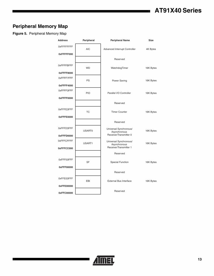
Peripheral Memory MapFigure 5. Peripheral Memory Map
Address Peripheral Peripheral Name Size
0xFFFFFFFF
0xFFFFF000
0xFFFFBFFF
0xFFFF8000
0xFFFF7FFF
0xFFFF4000
0xFFFF3FFF
0xFFFF0000
0xFFFE3FFF
0xFFFE0000
0xFFFCFFFF
0xFFFCC000
0xFFFD3FFF
0xFFFD0000
0xFFF03FFF
0xFFF00000
0xFFE03FFF
0xFFE00000
0xFFC00000
AIC
WD
PS
PIO
TC
USART1
USART0
SF
EBI
Advanced Interrupt Controller
Reserved
WatchdogTimer
Power Saving
Parallel I/O Controller
Reserved
Timer Counter
Universal Synchronous/Asynchronous
Receiver/Transmitter 1
Universal Synchronous/Asynchronous
Receiver/Transmitter 0
Reserved
Special Function
External Bus Interface
Reserved
4K Bytes
16K Bytes
16K Bytes
16K Bytes
16K Bytes
16K Bytes
16K Bytes
16K Bytes
16K Bytes
Reserved
Reserved
13
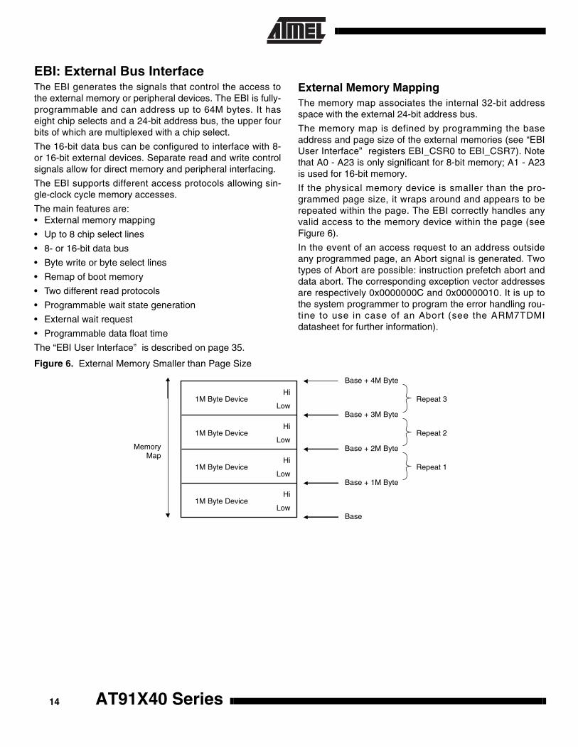
EBI: External Bus Interface The EBI generates the signals that control the access tothe external memory or peripheral devices. The EBI is fully-programmable and can address up to 64M bytes. It haseight chip selects and a 24-bit address bus, the upper fourbits of which are multiplexed with a chip select.
The 16-bit data bus can be configured to interface with 8-or 16-bit external devices. Separate read and write controlsignals allow for direct memory and peripheral interfacing.
The EBI supports different access protocols allowing sin-gle-clock cycle memory accesses.
The main features are:• External memory mapping
• Up to 8 chip select lines
• 8- or 16-bit data bus
• Byte write or byte select lines
• Remap of boot memory
• Two different read protocols
• Programmable wait state generation
• External wait request
• Programmable data float time
The “EBI User Interface” is described on page 35.
External Memory MappingThe memory map associates the internal 32-bit addressspace with the external 24-bit address bus.
The memory map is defined by programming the baseaddress and page size of the external memories (see “EBIUser Interface” registers EBI_CSR0 to EBI_CSR7). Notethat A0 - A23 is only significant for 8-bit memory; A1 - A23is used for 16-bit memory.
If the physical memory device is smaller than the pro-grammed page size, it wraps around and appears to berepeated within the page. The EBI correctly handles anyvalid access to the memory device within the page (seeFigure 6).
In the event of an access request to an address outsideany programmed page, an Abort signal is generated. Twotypes of Abort are possible: instruction prefetch abort anddata abort. The corresponding exception vector addressesare respectively 0x0000000C and 0x00000010. It is up tothe system programmer to program the error handling rou-tine to use in case of an Abort (see the ARM7TDMIdatasheet for further information).
Figure 6. External Memory Smaller than Page Size
1M Byte Device
1M Byte Device
1M Byte Device
1M Byte Device
MemoryMap
Hi
Low
Hi
Low
Hi
Low
Hi
LowBase
Base + 1M Byte
Base + 2M Byte
Base + 3M Byte
Base + 4M Byte
Repeat 1
Repeat 2
Repeat 3
AT91X40 Series14

AT91X40 Series
External Bus Interface Pin Description
The following table shows how certain EBI signals are multiplexed:
Name Description Type
A0 - A23 Address bus (output) Output
D0 - D15 Data bus (input/output) I/O
NCS0 - NCS3 Active low chip selects (output) Output
CS4 - CS7 Active high chip selects (output) Output
NRD Read enable (output) Output
NWR0 - NWR1 Lower and upper write enable (output) Output
NOE Output enable (output) Output
NWE Write enable (output) Output
NUB, NLB Upper and lower byte select (output) Output
NWAIT Wait request (input) Input
Table 4. EBI Signals
Multiplexed Signals Functions
A23 - A20 CS4 - CS7 Allows from 4 to 8 chip select lines to be used
A0 NLB 8- or 16-bit data bus
NRD NOE Byte write or byte select access
NWR0 NWE Byte write or byte select access
NWR1 NUB Byte write or byte select access
15
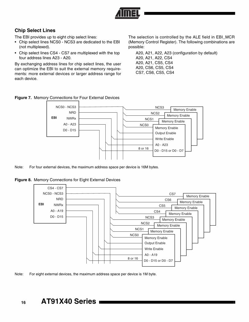
Chip Select LinesThe EBI provides up to eight chip select lines:• Chip select lines NCS0 - NCS3 are dedicated to the EBI
(not multiplexed).
• Chip select lines CS4 - CS7 are multiplexed with the top four address lines A23 - A20.
By exchanging address lines for chip select lines, the usercan optimize the EBI to suit the external memory require-ments: more external devices or larger address range foreach device.
The selection is controlled by the ALE field in EBI_MCR(Memory Control Register). The following combinations arepossible:
A20, A21, A22, A23 (configuration by default)A20, A21, A22, CS4A20, A21, CS5, CS4A20, CS6, CS5, CS4CS7, CS6, CS5, CS4
Figure 7. Memory Connections for Four External Devices
Note: For four external devices, the maximum address space per device is 16M bytes.
Figure 8. Memory Connections for Eight External Devices
Note: For eight external devices, the maximum address space per device is 1M byte.
EBI
NCS0 - NCS3
NRD
NWRx
A0 - A23
D0 - D15
NCS3
NCS2
NCS1
NCS0
8 or 16
Memory Enable
Memory Enable
Memory Enable
Memory Enable
Output Enable
Write Enable
A0 - A23
D0 - D15 or D0 - D7
EBI
NCS0 - NCS3
NRD
NWRx
A0 - A19
D0 - D15
CS7
CS6
CS5
CS4
8 or 16
Memory Enable
Memory Enable
Memory Enable
NCS3
NCS2
NCS1
NCS0
Memory Enable
Memory Enable
Memory Enable
Memory Enable
Memory Enable
Output Enable
Write Enable
A0 - A19
D0 - D15 or D0 - D7
CS4 - CS7
AT91X40 Series16

AT91X40 Series
Data Bus WidthA data bus width of 8 or 16 bits can be selected for eachchip select. This option is controlled by the DBW field in theEBI_CSR (Chip Select Register) for the corresponding chipselect.
Figure 9 shows how to connect a 512K x 8-bit memory onNCS2.
Figure 9. Memory Connection for an 8-Bit Data Bus
Figure 10 shows how to connect a 512K x 16-bit memoryon NCS2.
Figure 10. Memory Connection for a 16-bit Data Bus
Byte Write or Byte Select AccessEach chip select with a 16-bit data bus can operate withone of two different types of write access:• Byte Write Access supports two byte write and a single
read signal.
• Byte Select Access selects upper and/or lower byte with two byte select lines, and separate read and write signals.
This option is controlled by the BAT field in the EBI_CSR(Chip Select Register) for the corresponding chip select.
Byte Write Access is used to connect 2 x 8-bit devices as a16-bit memory page.• The signal A0/NLB is not used.
• The signal NWR1/NUB is used as NWR1 and enables upper byte writes.
• The signal NWR0/NWE is used as NWR0 and enables lower byte writes.
• The signal NRD/NOE is used as NRD and enables half-word and byte reads.
Figure 11 shows how to connect two 512K x 8-bit devicesin parallel on NCS2.
Figure 11. Memory Connection for 2 x 8-bit Data Busses
EBI
D0 - D7
D8 - D15
A1 - A18
A0
NWR0
NRD
NCS2
D0 - D7
A1 - A18
A0
Write Enable
Output Enable
Memory Enable
NWR1
EBI
D0 - D7
D8 - D15
A1 - A19
NLB
NWE
NOE
NCS2
D0 - D7
D8 - D15
A0 - A18
Low Byte Enable
Write Enable
Output Enable
Memory Enable
NUB High Byte Enable
EBI
D0 - D7
D8 - D15
A1 - A19
A0
NWR0
NRD
NCS2
D0 - D7
A0 - A18
Write Enable
Read Enable
Memory Enable
NWR1
D8 - D15
A0 - A18
Write Enable
Read Enable
Memory Enable
17
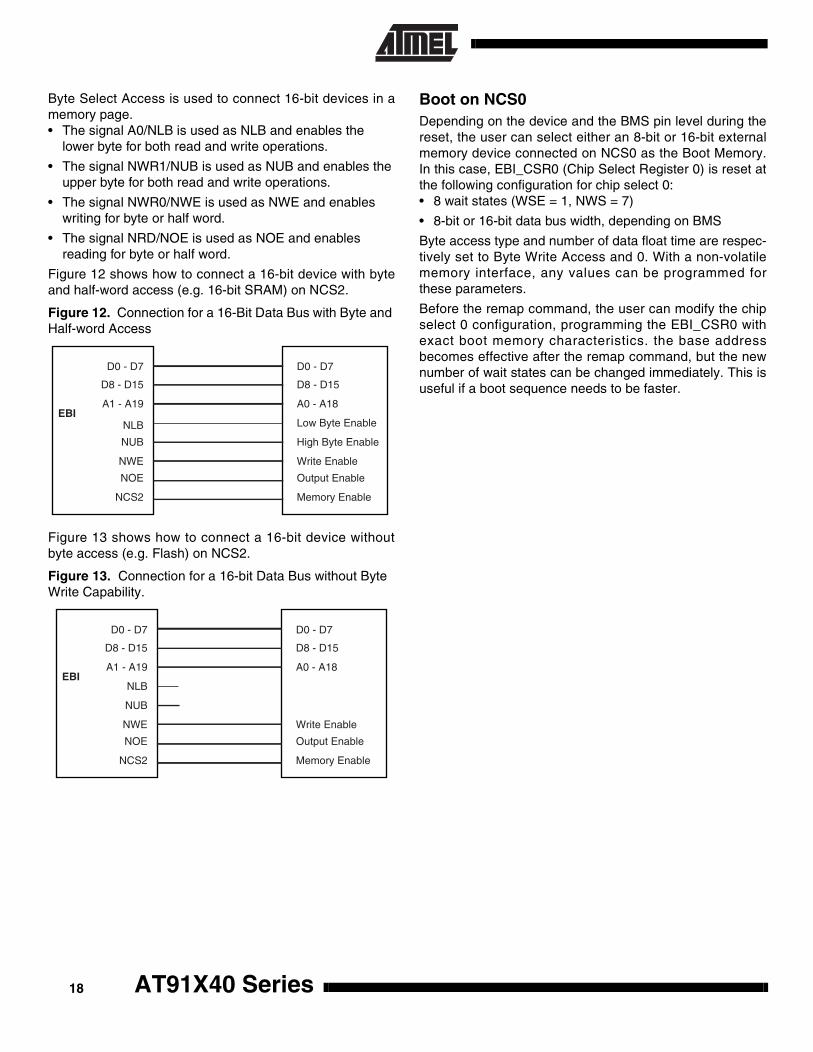
Byte Select Access is used to connect 16-bit devices in amemory page.• The signal A0/NLB is used as NLB and enables the
lower byte for both read and write operations.
• The signal NWR1/NUB is used as NUB and enables the upper byte for both read and write operations.
• The signal NWR0/NWE is used as NWE and enables writing for byte or half word.
• The signal NRD/NOE is used as NOE and enables reading for byte or half word.
Figure 12 shows how to connect a 16-bit device with byteand half-word access (e.g. 16-bit SRAM) on NCS2.
Figure 12. Connection for a 16-Bit Data Bus with Byte and Half-word Access
Figure 13 shows how to connect a 16-bit device withoutbyte access (e.g. Flash) on NCS2.
Figure 13. Connection for a 16-bit Data Bus without Byte Write Capability.
Boot on NCS0Depending on the device and the BMS pin level during thereset, the user can select either an 8-bit or 16-bit externalmemory device connected on NCS0 as the Boot Memory.In this case, EBI_CSR0 (Chip Select Register 0) is reset atthe following configuration for chip select 0:• 8 wait states (WSE = 1, NWS = 7)
• 8-bit or 16-bit data bus width, depending on BMS
Byte access type and number of data float time are respec-tively set to Byte Write Access and 0. With a non-volatilememory interface, any values can be programmed forthese parameters.
Before the remap command, the user can modify the chipselect 0 configuration, programming the EBI_CSR0 withexact boot memory characteristics. the base addressbecomes effective after the remap command, but the newnumber of wait states can be changed immediately. This isuseful if a boot sequence needs to be faster.
EBI
D0 - D7
D8 - D15
A1 - A19
NLB
NWE
NOE
NCS2
D0 - D7
D8 - D15
A0 - A18
Low Byte Enable
Write Enable
Output Enable
Memory Enable
NUB High Byte Enable
EBI
D0 - D7
D8 - D15
A1 - A19
NLB
NWE
NOE
NCS2
D0 - D7
D8 - D15
A0 - A18
Write Enable
Output Enable
Memory Enable
NUB
AT91X40 Series18

AT91X40 Series
Read ProtocolsThe EBI provides two alternative protocols for externalmemory read access: standard and early read. The differ-ence between the two protocols lies in the timing of theNRD (read cycle) waveform.
The protocol is selected by the DRP field in EBI_MCR(Memory Control Register) and is valid for all memorydevices. Standard read protocol is the default protocol afterreset.Note: In the following waveforms and descriptions, NRD repre-
sents NRD and NOE since the two signals have the same waveform. Likewise, NWE represents NWE, NWR0 and NWR1 unless NWR0 and NWR1 are other-wise represented. ADDR represents A0 - A23 and/or A1 - A23.
Standard Read Protocol
Standard read protocol implements a read cycle in whichNRD and NWE are similar. Both are active during the sec-ond half of the clock cycle. The first half of the clock cycleallows time to ensure completion of the previous access aswell as the output of address and NCS before the readcycle begins.
During a standard read protocol, external memory access,NCS is set low and ADDR is valid at the beginning of theaccess while NRD goes low only in the second half of themaster clock cycle to avoid bus conflict (see Figure 14).NWE is the same in both protocols. NWE always goes lowin the second half of the master clock cycle (see Figure 15).
Early Read Protocol
Early read protocol provides more time for a read accessfrom the memory by asserting NRD at the beginning of theclock cycle. In the case of successive read cycles in thesame memory, NRD remains active continuously. Since aread cycle normally limits the speed of operation of theexternal memory system, early read protocol can allow afaster clock frequency to be used. However, an extra waitstate is required in some cases to avoid contentions on theexternal bus.
Early Read Wait State
In early read protocol, an early read wait state is automati-cally inserted when an external write cycle is followed by aread cycle to allow time for the write cycle to end before thesubsequent read cycle begins (see Figure 16). This waitstate is generated in addition to any other programmed waitstates (i.e. data float wait).
No wait state is added when a read cycle is followed by awrite cycle, between consecutive accesses of the sametype or between external and internal memory accesses.
Early read wait states affect the external bus only. They donot affect internal bus timing.
Figure 14. Standard Read Protocol
Figure 15. Early Read Protocol
Figure 16. Early Read Wait State
ADDR
NCS
NWE
MCKI
NRD
or
ADDR
NCS
NWE
MCKI
NRD
or
ADDR
NCS
NWE
MCKI
Write Cycle Early Read Wait Read Cycle
NRD
19

Write Data Hold TimeDuring write cycles in both protocols, output data becomesvalid after the falling edge of the NWE signal and remainsvalid after the rising edge of NWE, as illustrated in Figure17. The external NWE waveform (on the NWE pin) is usedto control the output data t iming to guarantee thisoperation.
It is therefore necessary to avoid excessive loading of theNWE pins, which could delay the write signal too long andcause a contention with a subsequent read cycle in stan-dard protocol.
Figure 17. Data Hold Time
In early read protocol the data can remain valid longer thanin standard read protocol due to the additional wait cyclewhich follows a write access.
Wait StatesThe EBI can automatically insert wait states. The differenttypes of wait states are listed below:• Standard wait states
• Data float wait states
• External wait states
• Chip select change wait states
• Early read wait states (see “Read Protocols” )
Standard Wait States
Each chip select can be programmed to insert one or morewait states during an access on the corresponding device.This is done by setting the WSE field in the correspondingEBI_CSR. The number of cycles to insert is programmed inthe NWS field in the same register.
Below is the correspondence between the number of stan-dard wait states programmed and the number of cyclesduring which the NWE pulse is held low:
0 wait states1/2 cycle
1 wait state1 cycle
For each additional wait state programmed, an additionalcycle is added.
Figure 18. One Wait State Access
Notes: 1. Early Read Protocol
2. Standard Read Protocol
ADDR
NWE
Data Output
MCK
ADDR
NCS
NWE
MCK
1 Wait State Access
NRD (1) (2)
AT91X40 Series20
AT91X40 Series
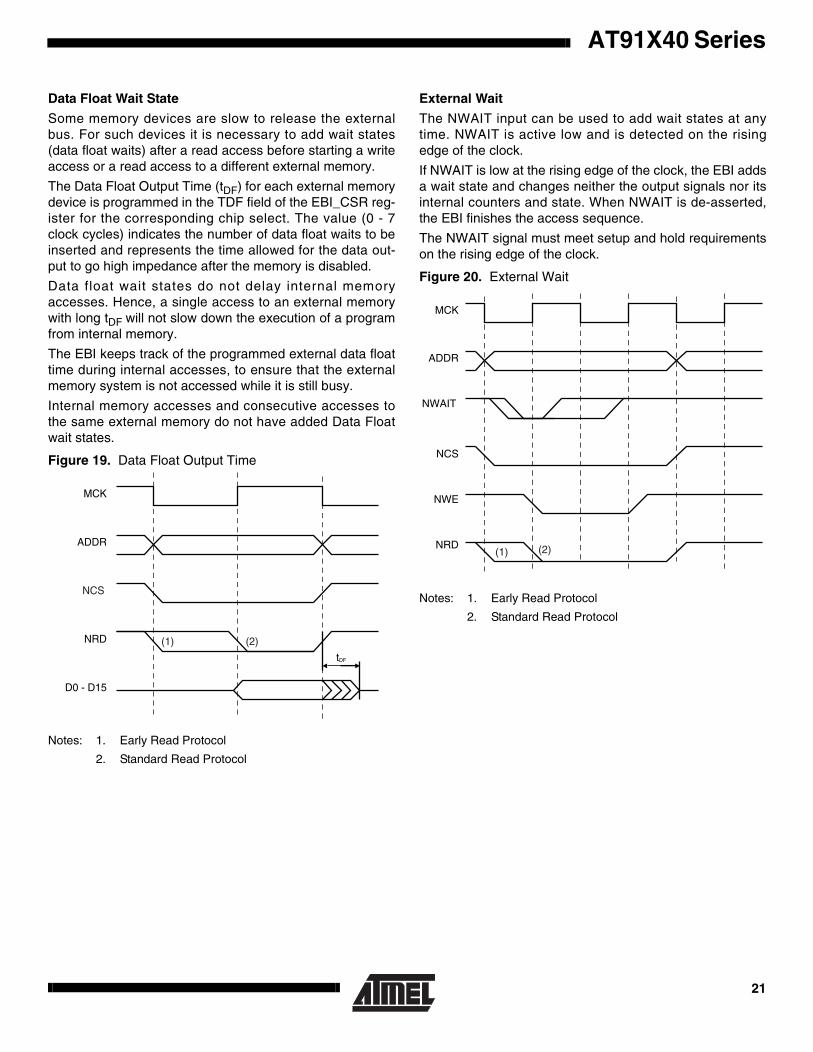
Data Float Wait State
Some memory devices are slow to release the externalbus. For such devices it is necessary to add wait states(data float waits) after a read access before starting a writeaccess or a read access to a different external memory.
The Data Float Output Time (tDF) for each external memorydevice is programmed in the TDF field of the EBI_CSR reg-ister for the corresponding chip select. The value (0 - 7clock cycles) indicates the number of data float waits to beinserted and represents the time allowed for the data out-put to go high impedance after the memory is disabled.
Data float wait states do not delay internal memoryaccesses. Hence, a single access to an external memorywith long tDF will not slow down the execution of a programfrom internal memory.
The EBI keeps track of the programmed external data floattime during internal accesses, to ensure that the externalmemory system is not accessed while it is still busy.
Internal memory accesses and consecutive accesses tothe same external memory do not have added Data Floatwait states.
Figure 19. Data Float Output Time
Notes: 1. Early Read Protocol
2. Standard Read Protocol
External Wait
The NWAIT input can be used to add wait states at anytime. NWAIT is active low and is detected on the risingedge of the clock.
If NWAIT is low at the rising edge of the clock, the EBI addsa wait state and changes neither the output signals nor itsinternal counters and state. When NWAIT is de-asserted,the EBI finishes the access sequence.
The NWAIT signal must meet setup and hold requirementson the rising edge of the clock.
Figure 20. External Wait
Notes: 1. Early Read Protocol
2. Standard Read Protocol
ADDR
NRD
D0 - D15
MCK
tDF
(1) (2)
NCS
ADDR
NCS
NWE
MCK
NRD(1) (2)
NWAIT
21

Chip Select Change Wait States
A chip select wait state is automatically inserted when con-secutive accesses are made to two different externalmemories (if no wait states have already been inserted). Ifany wait states have already been inserted, (e.g., data floatwait) then none are added.
Figure 21. Chip Select Wait
Notes: 1. Early Read Protocol
2. Standard Read Protocol
NCS1
NCS2
MCK
Mem 1 Chip Select Wait Mem 2
NRD
NWE
(1) (2)
AT91X40 Series22
AT91X40 Series
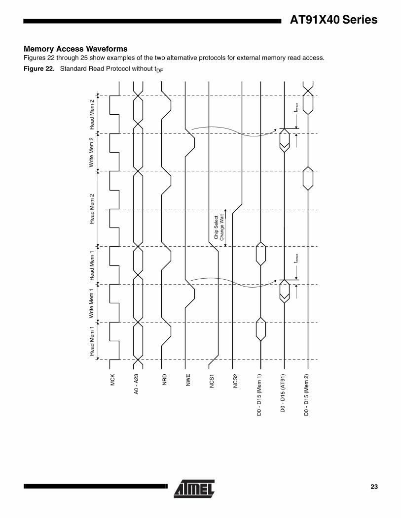
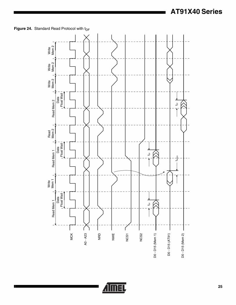
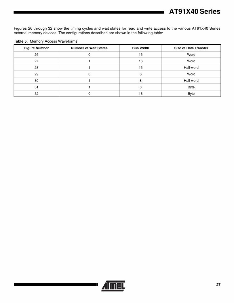
Memory Access WaveformsFigures 22 through 25 show examples of the two alternative protocols for external memory read access.
Figure 22. Standard Read Protocol without tDF
Rea
d M
em 1
Writ
e M
em 1
Rea
d M
em 1
Rea
d M
em 2
Writ
e M
em 2
Rea
d M
em 2
Chi
p S
elec
t C
hang
e W
ait
A0
- A
23
NR
D
NW
E
NC
S1
NC
S2
D0
- D
15 (
Mem
1)
D0
- D
15 (
Mem
2)
D0
- D
15 (
AT
91)
MC
K
t WH
DX
t WH
DX
23
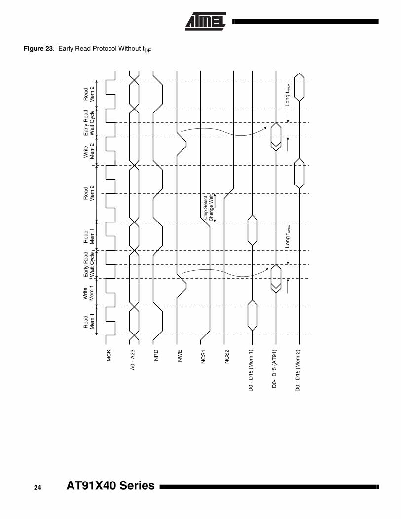
Figure 23. Early Read Protocol Without tDF
Rea
d M
em 1
Writ
e M
em 1
A0
- A
23
NR
D
NW
E
NC
S1
NC
S2
D0
- D
15 (
Mem
1)
D0
- D
15 (
Mem
2)
D0-
D15
(A
T91
)
MC
K
Ear
ly R
ead
Wai
t Cyc
leR
ead
Mem
1R
ead
Mem
2W
rite
Mem
2E
arly
Rea
dW
ait C
ycle
Rea
dM
em 2
Chi
p S
elec
tC
hang
e W
ait
Long
t WH
DX
Long
t WH
DX
AT91X40 Series24
AT91X40 Series
Figure 24. Standard Read Protocol with tDF
Rea
d M
em 1
Writ
e M
em 1
A0
- A
23
NR
D
NW
E
NC
S1
NC
S2
D0
- D
15 (
Mem
1)
D0
- D
15 (
Mem
2)
D0
- D
15 (
AT
91)
MC
K
Dat
aF
loat
Wai
t
Rea
d M
em 1 Dat
aF
loat
Wai
t
Rea
d M
em 2
Rea
d M
em 2 Dat
aF
loat
Wai
t
Writ
e M
em 2
Writ
e M
em 2
Writ
e M
em 2
t WH
DX
t DF
t DF
t DF
25
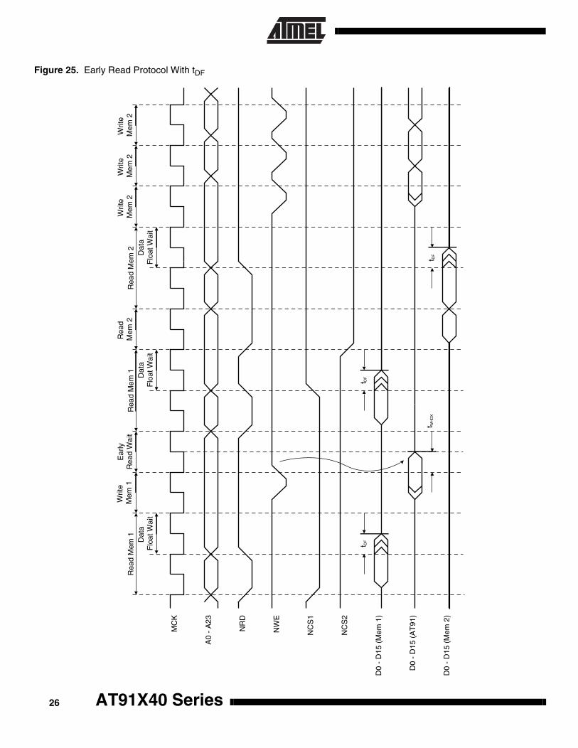
Figure 25. Early Read Protocol With tDF
Rea
d M
em 1
Writ
e M
em 1
A0
- A
23
NR
D
NW
E
NC
S1
NC
S2
D0
- D
15 (
Mem
1)
D0
- D
15 (
Mem
2)
D0
- D
15 (
AT
91)
MC
K
Dat
a F
loat
Wai
t
Ear
lyR
ead
Wai
tR
ead
Mem
1 Dat
aF
loat
Wai
t
Rea
d M
em 2
Rea
d M
em 2 Dat
aF
loat
Wai
t
Writ
e M
em 2
Writ
e M
em 2
Writ
e M
em 2
t DF
t DF
t DF
t WH
DX
AT91X40 Series26
AT91X40 Series
Figures 26 through 32 show the timing cycles and wait states for read and write access to the various AT91X40 Seriesexternal memory devices. The configurations described are shown in the following table:
Table 5. Memory Access Waveforms
Figure Number Number of Wait States Bus Width Size of Data Transfer
26 0 16 Word
27 1 16 Word
28 1 16 Half-word
29 0 8 Word
30 1 8 Half-word
31 1 8 Byte
32 0 16 Byte
27

Figure 26. 0 Wait States, 16-bit Bus Width, Word Transfer
ADDR ADDR+1
B2B1 B4 B3
B4 B3 B2 B1
MCK
A1 - A23
NCS
NRD
D0 - D15
Internal Bus X X B2 B1
READ ACCESS
NRD
B2 B1 B4 B3 D0 - D15
WRITE ACCESS
NWE
B2 B1 B4 B3 D0 - D15
NLB
NUB
· Standard Protocol
· Early Protocol
· Byte Write/ Byte Select Option
AT91X40 Series28

AT91X40 Series
Figure 27. 1 Wait, 16-bit Bus Width, Word Transfer
ADDR ADDR+1
B2B1
B4 B3
X X B2 B1 B4 B3 B2 B1
1 Wait State 1 Wair State
MCK
A1 - A23
NCS
NRD
D0 - D15
Internal Bus
WRITE ACCESS
READ ACCESS
NRD
D0 - D15
· Standard Protocol
· Early Protocol
B4B3
NWE
D0 - D15 B2B1 B4B3
NLB
NUB
B2 B1
· Byte Write/ Byte Select Option
29
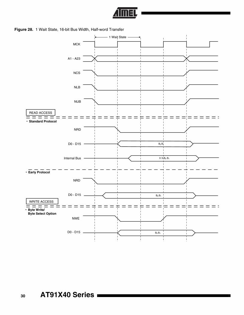
Figure 28. 1 Wait State, 16-bit Bus Width, Half-word Transfer
B2 B1
1 Wait State
MCK
A1 - A23
NCS
NRD
D0 - D15
Internal Bus X X B2 B1
READ ACCESS
· Standard Protocol
NLB
NUB
· Early Protocol
B2 B1
NRD
D0 - D15
WRITE ACCESS
NWE
B2 B1D0 - D15
· Byte Write/ Byte Select Option
AT91X40 Series30

AT91X40 Series
Figure 29. 0 Wait States, 8-bit Bus Width, Word Transfer
ADDR ADDR+1
X B1
X B3 B2 B1
MCK
A0 - A23
NCS
NRD
D0-D15
Internal Bus
ADDR+2 ADDR+3
X X B2 B1
X B2
X X X B1
X B3 X B4
B4 B3 B2 B1
READ ACCESS
· Standard Protocol
· Early Protocol
NRD
X B1D0 - D15 X B2 X B3 X B4
WRITE ACCESS
NWR0
NWR1
X B1D0 - D15 X B2 X B3 X B4
31

Figure 30. 1 Wait State, 8-bit Bus Width, Half-word Transfer
ADDR
X B1
1 Wait State
MCK
A0 - A23
NCS
NRD
D0 - D15
Internal Bus
ADDR+1
1 Wait State
X X B2 B1
X B2
X X X B1
READ ACCESS
· Standard Protocol
· Early Protocol
NRD
X B1D0 - D15 X B2
WRITE ACCESS
NWR0
X B1D0 - D15 X B2
NWR1
AT91X40 Series32

AT91X40 Series
Figure 31. 1 Wait State, 8-bit Bus Width, Byte Transfer
XB1
1 Wait State
MCK
A0 - A23
NCS
NRD
D0 - D15
Internal Bus X X X B1
READ ACCESS
· Standard Protocol
· Early Protocol
D0 - D15 X B1
WRITE ACCESS
NWR0
D0 - D15 X B1
NRD
NWR1
33
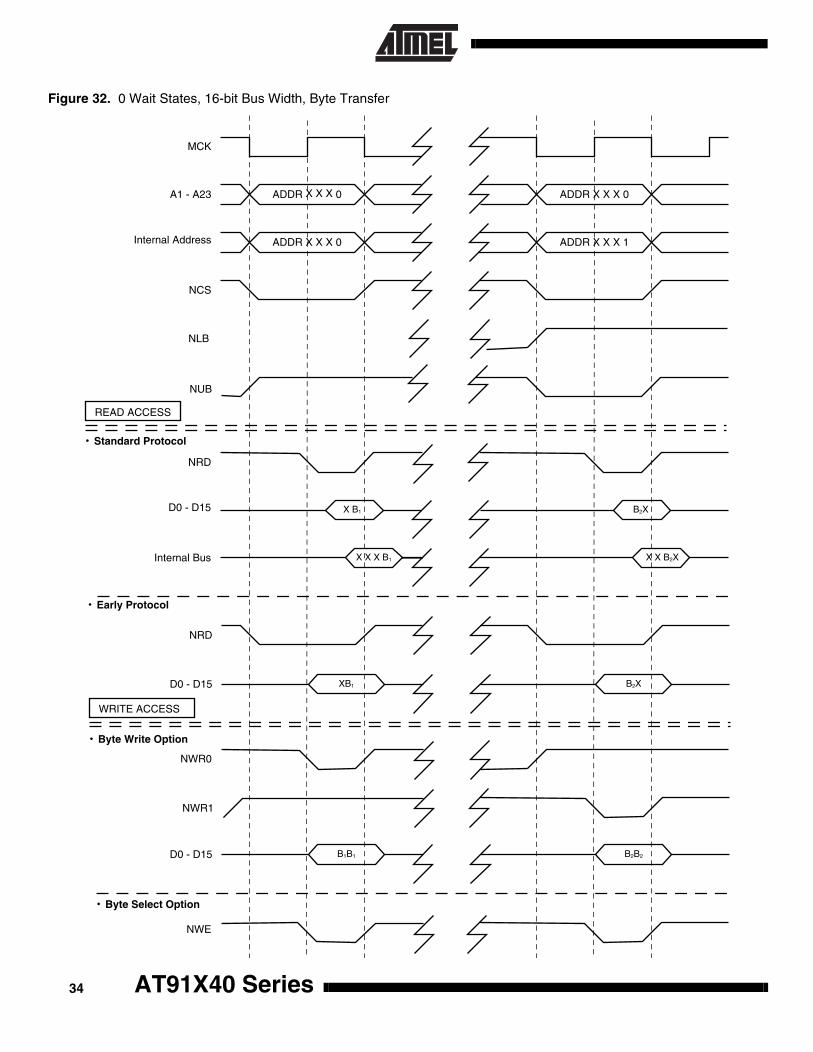
Figure 32. 0 Wait States, 16-bit Bus Width, Byte Transfer
MCK
A1 - A23
NCS
NWR1
D0 - D15 X B1 B2X
ADDR X X X 0 ADDR X X X 0
ADDR X X X 0 ADDR X X X 1Internal Address
Internal Bus X X X B1 X X B2X
NLB
NUB
READ ACCESS
· Standard Protocol
NRD
· Early Protocol
NRD
D0 - D15 XB1 B2X
WRITE ACCESS
NWR0
D0 - D15 B1B1 B2B2
· Byte Write Option
· Byte Select Option
NWE
AT91X40 Series34

AT91X40 Series
EBI User InterfaceThe EBI is programmed using the registers listed in thetable below. The Remap Control Register (EBI_RCR) con-trols exit from Boot Mode (see “Boot on NCS0” on page 18)The Memory Control Register (EBI_MCR) is used to pro-gram the number of active chip selects and data read
protocol. Eight Chip Select Registers (EBI_CSR0 toEBI_CSR7) are used to program the parameters for theindividual external memories. Each EBI_CSR must be pro-grammed with a different base address, even for unusedchip selects.
Base Address: 0xFFE00000
Notes: 1. 8-bit boot (if BMS is detected high)2. 16-bit boot (if BMS is detected low)
Table 6. EBI Memory Map
Offset Register Name Access Reset State
0x00 Chip Select Register 0 EBI_CSR0 Read/Write 0x0000203E (1)
0x0000203D (2)
0x04 Chip Select Register 1 EBI_CSR1 Read/Write 0x10000000
0x08 Chip Select Register 2 EBI_CSR2 Read/Write 0x20000000
0x0C Chip Select Register 3 EBI_CSR3 Read/Write 0x30000000
0x10 Chip Select Register 4 EBI_CSR4 Read/Write 0x40000000
0x14 Chip Select Register 5 EBI_CSR5 Read/Write 0x50000000
0x18 Chip Select Register 6 EBI_CSR6 Read/Write 0x60000000
0x1C Chip Select Register 7 EBI_CSR7 Read/Write 0x70000000
0x20 Remap Control Register EBI_RCR Write only –
0x24 Memory Control Register EBI_MCR Read/Write 0
35
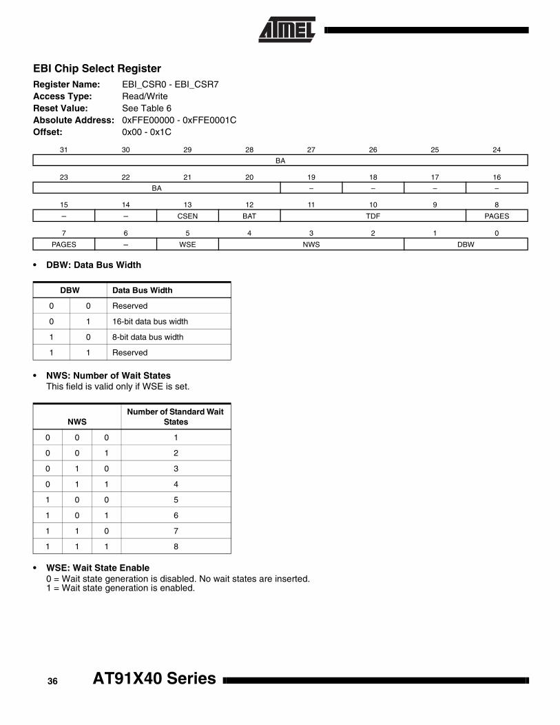
EBI Chip Select RegisterRegister Name: EBI_CSR0 - EBI_CSR7Access Type: Read/WriteReset Value: See Table 6Absolute Address: 0xFFE00000 - 0xFFE0001COffset: 0x00 - 0x1C
• DBW: Data Bus Width
• NWS: Number of Wait StatesThis field is valid only if WSE is set.
• WSE: Wait State Enable0 = Wait state generation is disabled. No wait states are inserted.1 = Wait state generation is enabled.
31 30 29 28 27 26 25 24
BA
23 22 21 20 19 18 17 16
BA – – – –
15 14 13 12 11 10 9 8
– – CSEN BAT TDF PAGES
7 6 5 4 3 2 1 0
PAGES – WSE NWS DBW
DBW Data Bus Width
0 0 Reserved
0 1 16-bit data bus width
1 0 8-bit data bus width
1 1 Reserved
NWSNumber of Standard Wait
States
0 0 0 1
0 0 1 2
0 1 0 3
0 1 1 4
1 0 0 5
1 0 1 6
1 1 0 7
1 1 1 8
AT91X40 Series36

AT91X40 Series
• PAGES: Page Size
• TDF: Data Float Output Time
• BAT: Byte Access Type0 = Byte write access type.1 = Byte select access type.
• CSEN: Chip Select Enable0 = Chip select is disabled.1 = Chip select is enabled.
• BA: Base AddressThese bits contain the highest bits of the base address. If the page size is larger than 1M byte, the unused bits of thebase address are ignored by the EBI decoder.
PAGES Page Size Active Bits in Base Address
0 0 1M Byte 12 Bits (31 - 20)
0 1 4M Bytes 10 Bits (31 - 22)
1 0 16M Bytes 8 Bits (31 - 24)
1 1 64M Bytes 6 Bits (31 - 26)
TDF Number of Cycles Added after the Transfer
0 0 0 0
0 0 1 1
0 1 0 2
0 1 1 3
1 0 0 4
1 0 1 5
1 1 0 6
1 1 1 7
37
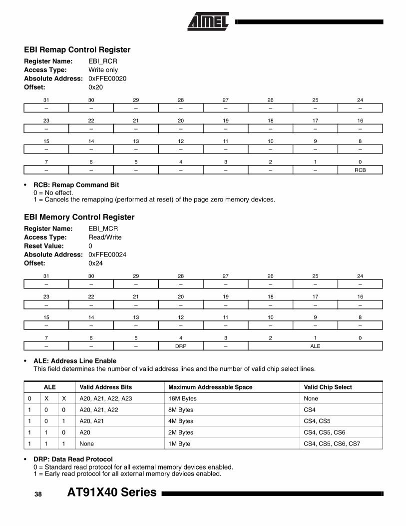
EBI Remap Control RegisterRegister Name: EBI_RCRAccess Type: Write onlyAbsolute Address: 0xFFE00020Offset: 0x20
• RCB: Remap Command Bit0 = No effect.1 = Cancels the remapping (performed at reset) of the page zero memory devices.
EBI Memory Control RegisterRegister Name: EBI_MCRAccess Type: Read/WriteReset Value: 0Absolute Address: 0xFFE00024Offset: 0x24
• ALE: Address Line EnableThis field determines the number of valid address lines and the number of valid chip select lines.
• DRP: Data Read Protocol0 = Standard read protocol for all external memory devices enabled.1 = Early read protocol for all external memory devices enabled.
31 30 29 28 27 26 25 24
– – – – – – – –
23 22 21 20 19 18 17 16
– – – – – – – –
15 14 13 12 11 10 9 8
– – – – – – – –
7 6 5 4 3 2 1 0
– – – – – – – RCB
31 30 29 28 27 26 25 24
– – – – – – – –
23 22 21 20 19 18 17 16
– – – – – – – –
15 14 13 12 11 10 9 8
– – – – – – – –
7 6 5 4 3 2 1 0
– – – DRP – ALE
ALE Valid Address Bits Maximum Addressable Space Valid Chip Select
0 X X A20, A21, A22, A23 16M Bytes None
1 0 0 A20, A21, A22 8M Bytes CS4
1 0 1 A20, A21 4M Bytes CS4, CS5
1 1 0 A20 2M Bytes CS4, CS5, CS6
1 1 1 None 1M Byte CS4, CS5, CS6, CS7
AT91X40 Series38

AT91X40 Series
PS: Power-saving The AT91X40 Series Power-saving feature enables optimi-zation of power consumption. The PS controls the CPUand Peripheral Clocks. One control register (PS_CR)enables the user to stop the ARM7TDMI Clock and enterIdle Mode. One set of registers with a set/clear mechanismenables and disables the peripheral clocks individually.
The ARM7TDMI clock is enabled after a reset and is auto-matically re-enabled by any enabled interrupt in the IdleMode.
Peripheral ClocksThe clock of each peripheral integrated in the AT91X40Series can be individually enabled and disabled by writingto the Peripheral Clock Enable (PS_PCER) and PeripheralClock Disable Registers (PS_PCDR). The status of theperipheral clocks can be read in the Peripheral Clock Sta-tus Register (PS_PCSR).
When a peripheral clock is disabled, the clock is immedi-ately stopped. When the clock is re-enabled, the peripheralresumes action where it left off.
To avoid data corruption or erroneous behavior of the sys-tem, the system software only disables the clock after allprogrammed peripheral operations have finished.
The peripheral clocks are automatically enabled after areset.
The bits that control the peripheral clocks are the same asthose that control the Interrupt Sources in the AIC.
39
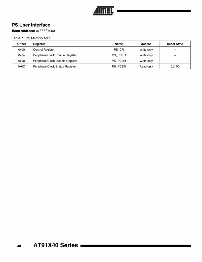
PS User InterfaceBase Address: 0xFFFF4000
Table 7. PS Memory Map
Offset Register Name Access Reset State
0x00 Control Register PS_CR Write only –
0x04 Peripheral Clock Enable Register PS_PCER Write only –
0x08 Peripheral Clock Disable Register PS_PCDR Write only –
0x0C Peripheral Clock Status Register PS_PCSR Read only 0x17C
AT91X40 Series40

AT91X40 Series
PS Control RegisterName: PS_CRAccess: Write onlyOffset: 0x00
• CPU: CPU Clock Disable 0 = No effect.1 = Disables the CPU clock.The CPU clock is re-enabled by any enabled interrupt or by hardware reset.
31 30 29 28 27 26 25 24
– – – – – – – –
23 22 21 20 19 18 17 16
– – – – – – – –
15 14 13 12 11 10 9 8
– – – – – – – –
7 6 5 4 3 2 1 0
– – – – – – – CPU
41
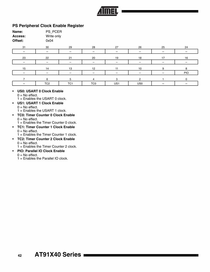
PS Peripheral Clock Enable RegisterName: PS_PCERAccess: Write onlyOffset: 0x04
• US0: USART 0 Clock Enable 0 = No effect.1 = Enables the USART 0 clock.
• US1: USART 1 Clock Enable0 = No effect.1 = Enables the USART 1 clock.
• TC0: Timer Counter 0 Clock Enable0 = No effect.1 = Enables the Timer Counter 0 clock.
• TC1: Timer Counter 1 Clock Enable0 = No effect.1 = Enables the Timer Counter 1 clock.
• TC2: Timer Counter 2 Clock Enable0 = No effect.1 = Enables the Timer Counter 2 clock.
• PIO: Parallel IO Clock Enable0 = No effect.1 = Enables the Parallel IO clock.
31 30 29 28 27 26 25 24
– – – – – – – –
23 22 21 20 19 18 17 16
– – – – – – – –
15 14 13 12 11 10 9 8
– – – – – – – PIO
7 6 5 4 3 2 1 0
– TC2 TC1 TC0 US1 US0 – –
AT91X40 Series42
AT91X40 Series
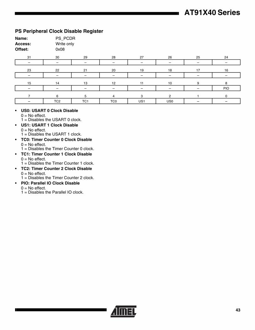
PS Peripheral Clock Disable RegisterName: PS_PCDRAccess: Write only Offset: 0x08
• US0: USART 0 Clock Disable 0 = No effect.1 = Disables the USART 0 clock.
• US1: USART 1 Clock Disable0 = No effect.1 = Disables the USART 1 clock.
• TC0: Timer Counter 0 Clock Disable0 = No effect.1 = Disables the Timer Counter 0 clock.
• TC1: Timer Counter 1 Clock Disable0 = No effect.1 = Disables the Timer Counter 1 clock.
• TC2: Timer Counter 2 Clock Disable0 = No effect.1 = Disables the Timer Counter 2 clock.
• PIO: Parallel IO Clock Disable0 = No effect.1 = Disables the Parallel IO clock.
31 30 29 28 27 26 25 24
– – – – – – – –
23 22 21 20 19 18 17 16
– – – – – – – –
15 14 13 12 11 10 9 8
– – – – – – – PIO
7 6 5 4 3 2 1 0
– TC2 TC1 TC0 US1 US0 – –
43

PS Peripheral Clock Status RegisterName: PS_PCSRAccess: Read onlyReset Value: 0x17COffset: 0x0C
• US0: USART 0 Clock Status 0 = USART 0 clock is disabled. 1 = USART 0 clock is enabled.
• US1: USART 1 Clock Status0 = USART 1 clock is disabled. 1 = USART 1 clock is enabled.
• TC0: Timer Counter 0 Clock Status0 = Timer Counter 0 clock is disabled. 1 = Timer Counter 0 clock is enabled.
• TC1: Timer Counter 1 Clock Status0 = Timer Counter 1 clock is disabled. 1 = Timer Counter 1 clock is enabled.
• TC2: Timer Counter 2 Clock Status0 = Timer Counter 2 clock is disabled. 1 = Timer Counter 2 clock is enabled.
• PIO: Parallel IO Clock Status0 = Parallel IO clock is disabled. 1 = Parallel IO clock is enabled.
31 30 29 28 27 26 25 24
– – – – – – – –
23 22 21 20 19 18 17 16
– – – – – – – –
15 14 13 12 11 10 9 8
– – – – – – – PIO
7 6 5 4 3 2 1 0
– TC2 TC1 TC0 US1 US0 – –
AT91X40 Series44
AT91X40 Series
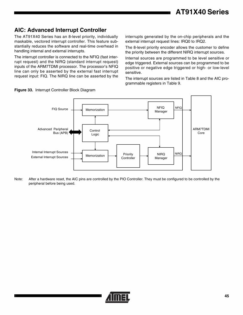
AIC: Advanced Interrupt Controller The AT91X40 Series has an 8-level priority, individuallymaskable, vectored interrupt controller. This feature sub-stantially reduces the software and real-time overhead inhandling internal and external interrupts.
The interrupt controller is connected to the NFIQ (fast inter-rupt request) and the NIRQ (standard interrupt request)inputs of the ARM7TDMI processor. The processor’s NFIQline can only be asserted by the external fast interruptrequest input: FIQ. The NIRQ line can be asserted by the
interrupts generated by the on-chip peripherals and theexternal interrupt request lines: IRQ0 to IRQ2.
The 8-level priority encoder allows the customer to definethe priority between the different NIRQ interrupt sources.
Internal sources are programmed to be level sensitive oredge triggered. External sources can be programmed to bepositive or negative edge triggered or high- or low-levelsensitive.
The interrupt sources are listed in Table 8 and the AIC pro-grammable registers in Table 9.
Figure 33. Interrupt Controller Block Diagram
Note: After a hardware reset, the AIC pins are controlled by the PIO Controller. They must be configured to be controlled by the peripheral before being used.
Control Logic
Memorization
Memorization PriorityController
NIRQManager
NFIQ Manager
FIQ Source
Advanced PeripheralBus (APB)
Internal Interrupt Sources
External Interrupt Sources
ARM7TDMICore
NFIQ
NIRQ
45

Notes: 1. Reserved interrupt sources are not available. Corresponding registers must not be used and read 0.
Table 8. AIC Interrupt Sources
Interrupt Source (1) Interrupt Name Interrupt Description
0 FIQ Fast Interrupt
1 SWIRQ Software Interrupt
2 US0IRQ USART Channel 0 interrupt
3 US1IRQ USART Channel 1 interrupt
4 TC0IRQ Timer Channel 0 interrupt
5 TC1IRQ Timer Channel 1 interrupt
6 TC2IRQ Timer Channel 2 interrupt
7 WDIRQ Watchdog interrupt
8 PIOIRQ Parallel I/O Controller interrupt
9 – Reserved
10 – Reserved
11 – Reserved
12 – Reserved
13 – Reserved
14 – Reserved
15 – Reserved
16 IRQ0 External interrupt 0
17 IRQ1 External interrupt 1
18 IRQ2 External interrupt 2
19 – Reserved
20 – Reserved
21 – Reserved
22 – Reserved
23 – Reserved
24 – Reserved
25 – Reserved
26 – Reserved
27 – Reserved
28 – Reserved
29 – Reserved
30 – Reserved
31 – Reserved
AT91X40 Series46

AT91X40 Series
Hardware Interrupt VectoringThe hardware interrupt vectoring reduces the number ofinstructions to reach the interrupt handler to only one. Bystoring the following instruction at address 0x00000018,the processor loads the program counter with the interrupthandler address stored in the AIC_IVR register. Executionis then vectored to the interrupt handler corresponding tothe current interrupt.
ldr PC,[PC,# - &F20]
The current interrupt is the interrupt with the highest prioritywhen the Interrupt Vector Register (AIC_IVR) is read. Thevalue read in the AIC_IVR corresponds to the addressstored in the Source Vector Register (AIC_SVR) of the cur-rent interrupt. Each interrupt source has its correspondingAIC_SVR. In order to take advantage of the hardware inter-rupt vectoring it is necessary to store the address of eachinterrupt handler in the corresponding AIC_SVR, at systeminitialization.
Priority ControllerThe NIRQ line is controlled by an 8-level priority encoder.Each source has a programmable priority level of 7 to 0.Level 7 is the highest priority and level 0 the lowest.
When the AIC receives more than one unmasked interruptat a time, the interrupt with the highest priority is servicedfirst. If both interrupts have equal priority, the interrupt withthe lowest interrupt source number (see table 8) is servicedfirst.
The current priority level is defined as the priority level ofthe current interrupt at the time the register AIC_IVR is read(the interrupt which will be serviced).
In the case when a higher priority unmasked interruptoccurs while an interrupt already exists, there are two pos-sible outcomes depending on whether the AIC_IVR hasbeen read.• If the NIRQ line has been asserted but the AIC_IVR has
not been read, then the processor will read the new higher priority interrupt handler address in the AIC_IVR register and the current interrupt level is updated.
• If the processor has already read the AIC_IVR then the NIRQ line is reasserted. When the processor has authorized nested interrupts to occur and reads the AIC_IVR again, it reads the new, higher priority interrupt handler address. At the same time the current priority value is pushed onto a first-in last-out stack and the current priority is updated to the higher priority.
When the end of interrupt command register (AIC_EOICR)is written the current interrupt level is updated with the laststored interrupt level from the stack (if any). Hence at theend of a higher priority interrupt, the AIC returns to the pre-
vious state corresponding to the preceding lower priorityinterrupt which had been interrupted.
Interrupt HandlingThe interrupt handler must read the AIC_IVR as soon aspossible. This de-asserts the NIRQ request to the proces-sor and clears the interrupt in case it is programmed to beedge triggered. This permits the AIC to assert the NIRQline again when a higher priority unmasked interruptoccurs.
At the end of the interrupt service routine, the end of inter-rupt command register (AIC_EOICR) must be written. Thisallows pending interrupts to be serviced.
Interrupt MaskingEach interrupt source, including FIQ, can be enabled ordisabled using the command registers AIC_IECR andAIC_IDCR. The interrupt mask can be read in the read onlyregister AIC_IMR. A disabled interrupt does not affect theservicing of other interrupts.
Interrupt Clearing and SettingAll interrupt sources which are programmed to be edge trig-gered (including FIQ) can be individually set or cleared byrespectively writ ing to the registers AIC_ISCR andAIC_ICCR. This function of the interrupt controller is avail-able for auto-test or software debug purposes.
Fast Interrupt RequestThe external FIQ line is the only source which can raise afast interrupt request to the processor. Therefore, it has nopriority controller.
The external FIQ line can be programmed to be positive ornegative edge triggered or high- or low-level sensitive inthe AIC_SMR0 register.
The fast interrupt handler address can be stored in theAIC_SVR0 register. The value written into this register isavailable by reading the AIC_FVR register when an FIQinterrupt is raised. By storing the following instruction ataddress 0x0000001C, the processor will load the programcounter with the interrupt handler address stored in theAIC_FVR register.
ldr PC,[PC,# -&F20]
Alternatively the interrupt handler can be stored startingfrom address 0x0000001C as described in the ARM7TDMIdatasheet.
Software InterruptInterrupt source 1 of the advanced interrupt controller is asoftware interrupt. It must be programmed to be edge trig-
47
gered in order to set or clear it by writing to the AIC_ISCRand AIC_ICCR.
This is totally independent of the SWI instruction of theARM7TDMI processor.
Spurious InterruptWhen the AIC asserts the NIRQ line, the ARM7TDMIenters IRQ Mode and the interrupt handler reads the IVR. Itmay happen that the AIC de-asserts the NIRQ line after thecore has taken into account the NIRQ assertion and beforethe read of the IVR.
This behavior is called a Spurious Interrupt.
The AIC is able to detect these Spurious Interrupts andreturns the Spurious Vector when the IVR is read. The Spu-rious Vector can be programmed by the user when thevector table is initialized.
A spurious interrupt may occur in the following cases:• With any sources programmed to be level sensitive, if the
interrupt signal of the AIC input is de-asserted at the same time as it is taken into account by the ARM7TDMI.
• If an interrupt is asserted at the same time as the software is disabling the corresponding source through AIC_IDCR (this can happen due to the pipelining of the ARM core).
The same mechanism of spurious interrupt occurs if theARM7TDMI reads the IVR (application software or ICE)when there is no interrupt pending. This mechanism is alsovalid for the FIQ interrupts.
Once the AIC enters the spurious interrupt management, itasserts neither the NIRQ nor the NFIQ lines to theARM7TDMI as long as the spurious interrupt is notacknowledged. Therefore, it is mandatory for the SpuriousInterrupt Service Routine to acknowledge the “spurious”behavior by writing to the AIC_EOICR (End of Interrupt)before returning to the interrupted software. It also can per-form other operation(s), e.g., trace possible undesirablebehavior.
Protect ModeThe Protect Mode permits reading of the Interrupt VectorRegister without performing the associated automatic oper-ations. This is necessary when working with a debugsystem.
When a Debug Monitor or an ICE reads the AIC User Inter-face, the IVR could be read. This would have the followingconsequences in Normal Mode.• If an enabled interrupt with a higher priority than the
current one is pending, it would be stacked
• If there is no enabled pending interrupt, the spurious vector would be returned
In either case, an End of Interrupt command would be nec-essary to acknowledge and to restore the context of theAIC. This operation is generally not performed by thedebug system. Hence the debug system would becomestrongly intrusive, and could cause the application to enteran undesired state.
This is avoided by using Protect Mode.
The Protect Mode is enabled by setting the AIC bit in theSF Protect Mode Register (see SF: Special Function Reg-isters on page 80).
When Protect Mode is enabled, the AIC performs interruptstacking only when a write access is performed on theAIC_IVR. Therefore, the Interrupt Service Routines mustwrite (arbitrary data) to the AIC_IVR just after reading it.
The new context of the AIC, including the value of the Inter-rupt Status Register (AIC_ISR), is updated with the currentinterrupt only when IVR is written.
An AIC_IVR read on its own (e.g. by a debugger), modifiesneither the AIC context nor the AIC_ISR.
Extra AIC_IVR reads performed in between the read andthe write can cause unpredictable results. Therefore, it isstrongly recommended not to set a breakpoint betweenthese 2 actions, nor to stop the software.
The debug system must not write to the AIC_IVR as thiswould cause undesirable effects.
The following table shows the main steps of an interruptand the order in which they are performed according to themode:
Notes: 1. NIRQ de-assertion and automatic interrupt clearing if the source is programmed as level sensitive.
2. Software that has been written and debugged using Protect Mode will run correctly in Normal Mode with-out modification. However, in Normal Mode the AIC_IVR write has no effect and can be removed to optimize the code.
ActionNormal Mode
Protect Mode
Calculate active interrupt (higher than current or spurious)
ReadAIC_IVR
ReadAIC_IVR
Determine and return the vector of the active interrupt
ReadAIC_IVR
ReadAIC_IVR
Memorize interrupt ReadAIC_IVR
ReadAIC_IVR
Push on internal stack the current priority level
ReadAIC_IVR
WriteAIC_IVR
Acknowledge the interrupt (1) ReadAIC_IVR
WriteAIC_IVR
No effect (2) WriteAIC_IVR –
AT91X40 Series48
AT91X40 Series
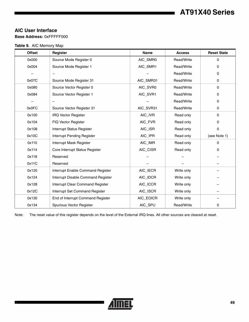
AIC User InterfaceBase Address: 0xFFFFF000
Note: The reset value of this register depends on the level of the External IRQ lines. All other sources are cleared at reset.
Table 9. AIC Memory Map
Offset Register Name Access Reset State
0x000 Source Mode Register 0 AIC_SMR0 Read/Write 0
0x004 Source Mode Register 1 AIC_SMR1 Read/Write 0
– – – Read/Write 0
0x07C Source Mode Register 31 AIC_SMR31 Read/Write 0
0x080 Source Vector Register 0 AIC_SVR0 Read/Write 0
0x084 Source Vector Register 1 AIC_SVR1 Read/Write 0
– – – Read/Write 0
0x0FC Source Vector Register 31 AIC_SVR31 Read/Write 0
0x100 IRQ Vector Register AIC_IVR Read only 0
0x104 FIQ Vector Register AIC_FVR Read only 0
0x108 Interrupt Status Register AIC_ISR Read only 0
0x10C Interrupt Pending Register AIC_IPR Read only (see Note 1)
0x110 Interrupt Mask Register AIC_IMR Read only 0
0x114 Core Interrupt Status Register AIC_CISR Read only 0
0x118 Reserved – – –
0x11C Reserved – – –
0x120 Interrupt Enable Command Register AIC_IECR Write only –
0x124 Interrupt Disable Command Register AIC_IDCR Write only –
0x128 Interrupt Clear Command Register AIC_ICCR Write only –
0x12C Interrupt Set Command Register AIC_ISCR Write only –
0x130 End of Interrupt Command Register AIC_EOICR Write only –
0x134 Spurious Vector Register AIC_SPU Read/Write 0
49

AIC Source Mode RegisterRegister Name: AIC_SMR0 - AIC_SMR31Access Type: Read/WriteReset Value: 0Offset: 0x000 - 0x07C
• PRIOR: Priority LevelProgram the priority level for all sources except source 0 (FIQ).The priority level can be between 0 (lowest) and 7 (highest).The priority level is not used for the FIQ, in the SMR0.
• SRCTYPE: Interrupt Source TypeProgram the input to be positive or negative edge triggered or positive or negative level sensitive. The active level or edge is not programmable for the internal sources.
31 30 29 28 27 26 25 24
– – – – – – – –
23 22 21 20 19 18 17 16
– – – – – – – –
15 14 13 12 11 10 9 8
– – – – – – – –
7 6 5 4 3 2 1 0
– SRCTYPE – – PRIOR
SRCTYPE Internal Sources External Sources
0 0 Level Sensitive Low Level Sensitive
0 1 Edge Triggered Negative Edge Triggered
1 0 Level Sensitive High Level Sensitive
1 1 Edge Triggered Positive Edge Triggered
AT91X40 Series50
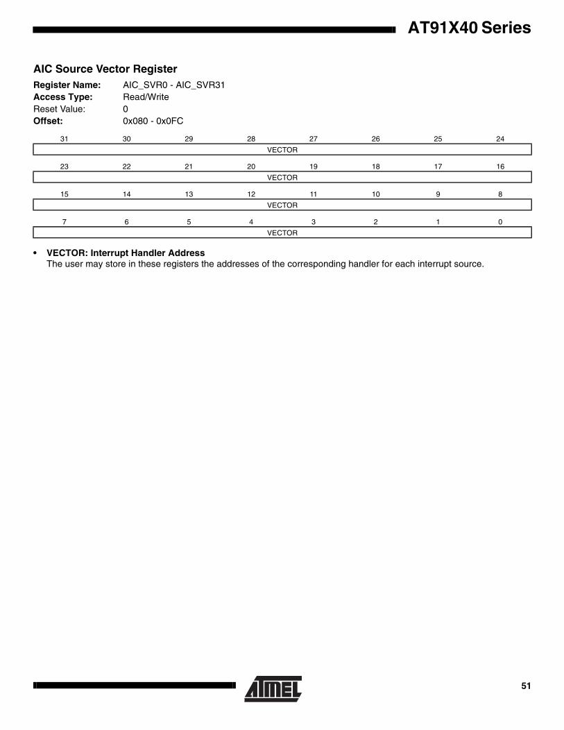
AT91X40 Series
AIC Source Vector RegisterRegister Name: AIC_SVR0 - AIC_SVR31Access Type: Read/WriteReset Value: 0Offset: 0x080 - 0x0FC
• VECTOR: Interrupt Handler AddressThe user may store in these registers the addresses of the corresponding handler for each interrupt source.
31 30 29 28 27 26 25 24
VECTOR
23 22 21 20 19 18 17 16
VECTOR
15 14 13 12 11 10 9 8
VECTOR
7 6 5 4 3 2 1 0
VECTOR
51
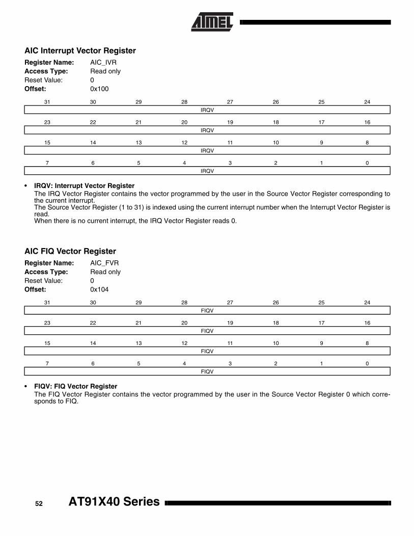
AIC Interrupt Vector RegisterRegister Name: AIC_IVRAccess Type: Read onlyReset Value: 0Offset: 0x100
• IRQV: Interrupt Vector RegisterThe IRQ Vector Register contains the vector programmed by the user in the Source Vector Register corresponding tothe current interrupt.The Source Vector Register (1 to 31) is indexed using the current interrupt number when the Interrupt Vector Register isread.When there is no current interrupt, the IRQ Vector Register reads 0.
AIC FIQ Vector RegisterRegister Name: AIC_FVRAccess Type: Read onlyReset Value: 0Offset: 0x104
• FIQV: FIQ Vector RegisterThe FIQ Vector Register contains the vector programmed by the user in the Source Vector Register 0 which corre-sponds to FIQ.
31 30 29 28 27 26 25 24
IRQV
23 22 21 20 19 18 17 16
IRQV
15 14 13 12 11 10 9 8
IRQV
7 6 5 4 3 2 1 0
IRQV
31 30 29 28 27 26 25 24
FIQV
23 22 21 20 19 18 17 16
FIQV
15 14 13 12 11 10 9 8
FIQV
7 6 5 4 3 2 1 0
FIQV
AT91X40 Series52
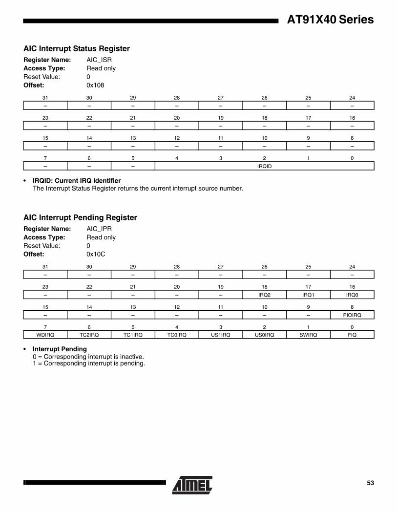
AT91X40 Series
AIC Interrupt Status RegisterRegister Name: AIC_ISRAccess Type: Read onlyReset Value: 0Offset: 0x108
• IRQID: Current IRQ IdentifierThe Interrupt Status Register returns the current interrupt source number.
AIC Interrupt Pending RegisterRegister Name: AIC_IPRAccess Type: Read onlyReset Value: 0Offset: 0x10C
• Interrupt Pending0 = Corresponding interrupt is inactive.1 = Corresponding interrupt is pending.
31 30 29 28 27 26 25 24
– – – – – – – –
23 22 21 20 19 18 17 16
– – – – – – – –
15 14 13 12 11 10 9 8
– – – – – – – –
7 6 5 4 3 2 1 0
– – – IRQID
31 30 29 28 27 26 25 24
– – – – – – – –
23 22 21 20 19 18 17 16
– – – – – IRQ2 IRQ1 IRQ0
15 14 13 12 11 10 9 8
– – – – – – – PIOIRQ
7 6 5 4 3 2 1 0
WDIRQ TC2IRQ TC1IRQ TC0IRQ US1IRQ US0IRQ SWIRQ FIQ
53
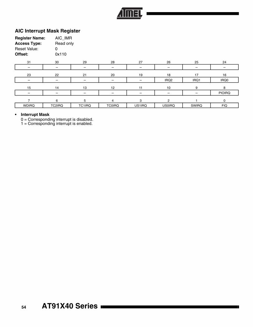
AIC Interrupt Mask RegisterRegister Name: AIC_IMRAccess Type: Read onlyReset Value: 0Offset: 0x110
• Interrupt Mask0 = Corresponding interrupt is disabled. 1 = Corresponding interrupt is enabled.
31 30 29 28 27 26 25 24
– – – – – – – –
23 22 21 20 19 18 17 16
– – – – – IRQ2 IRQ1 IRQ0
15 14 13 12 11 10 9 8
– – – – – – – PIOIRQ
7 6 5 4 3 2 1 0
WDIRQ TC2IRQ TC1IRQ TC0IRQ US1IRQ US0IRQ SWIRQ FIQ
AT91X40 Series54

AT91X40 Series
AIC Core Interrupt Status RegisterRegister Name: AIC_CISRAccess Type: Read onlyReset Value: 0Offset: 0x114
• NFIQ: NFIQ Status 0 = NFIQ line inactive.1 = NFIQ line active.
• NIRQ: NIRQ Status0 = NIRQ line inactive.1 = NIRQ line active.
31 30 29 28 27 26 25 24
– – – – – – – –
23 22 21 20 19 18 17 16
– – – – – – – –
15 14 13 12 11 10 9 8
– – – – – – – –
7 6 5 4 3 2 1 0
– – – – – – NIRQ NFIQ
55

AIC Interrupt Enable Command RegisterRegister Name: AIC_IECRAccess Type: Write onlyOffset: 0x120
• Interrupt Enable0 = No effect.1 = Enables corresponding interrupt.
AIC Interrupt Disable Command RegisterRegister Name: AIC_IDCRAccess Type: Write onlyOffset: 0x124
• Interrupt Disable0 = No effect.1 = Disables corresponding interrupt.
31 30 29 28 27 26 25 24
– – – – – – – –
23 22 21 20 19 18 17 16
– – – – – IRQ2 IRQ1 IRQ0
15 14 13 12 11 10 9 8
– – – – – – – PIOIRQ
7 6 5 4 3 2 1 0
WDIRQ TC2IRQ TC1IRQ TC0IRQ US1IRQ US0IRQ SWIRQ FIQ
31 30 29 28 27 26 25 24
– – – – – – – –
23 22 21 20 19 18 17 16
– – – – – IRQ2 IRQ1 IRQ0
15 14 13 12 11 10 9 8
– – – – – – – PIOIRQ
7 6 5 4 3 2 1 0
WDIRQ TC2IRQ TC1IRQ TC0IRQ US1IRQ US0IRQ SWIRQ FIQ
AT91X40 Series56

AT91X40 Series
AIC Interrupt Clear Command RegisterRegister Name: AIC_ICCRAccess Type: Write onlyOffset: 0x128
• Interrupt Clear0 = No effect.1 = Clears corresponding interrupt.
AIC Interrupt Set Command RegisterRegister Name: AIC_ISCRAccess Type: Write onlyOffset: 0x12C
• Interrupt Set0 = No effect.1 = Sets corresponding interrupt.
31 30 29 28 27 26 25 24
– – – – – – – –
23 22 21 20 19 18 17 16
– – – – – IRQ2 IRQ1 IRQ0
15 14 13 12 11 10 9 8
– – – – – – – PIOIRQ
7 6 5 4 3 2 1 0
WDIRQ TC2IRQ TC1IRQ TC0IRQ US1IRQ US0IRQ SWIRQ FIQ
31 30 29 28 27 26 25 24
– – – – – – – –
23 22 21 20 19 18 17 16
– – – – – IRQ2 IRQ1 IRQ0
15 14 13 12 11 10 9 8
– – – – – – – PIOIRQ
7 6 5 4 3 2 1 0
WDIRQ TC2IRQ TC1IRQ TC0IRQ US1IRQ US0IRQ SWIRQ FIQ
57

AIC End of Interrupt Command RegisterRegister Name: AIC_EOICRAccess Type: Write onlyOffset: 0x130
The End of Interrupt Command Register is used by the interrupt routine to indicate that the interrupt treatment is complete.Any value can be written because it is only necessary to make a write to this register location to signal the end of interrupttreatment.
AIC Spurious Vector RegisterRegister Name: AIC_SPUAccess Type: Read/WriteReset Value: 0Offset: 0x134
• SPUVEC: Spurious Interrupt Vector Handler AddressThe user may store the address of the spurious interrupt handler in this register.
31 30 29 28 27 26 25 24
– – – – – – – –
23 22 21 20 19 18 17 16
– – – – – – – –
15 14 13 12 11 10 9 8
– – – – – – – –
7 6 5 4 3 2 1 0
– – – – – – – –
31 30 29 28 27 26 25 24
SPUVEC
23 22 21 20 19 18 17 16
SPUVEC
15 14 13 12 11 10 9 8
SPUVEC
7 6 5 4 3 2 1 0
SPUVEC
AT91X40 Series58
AT91X40 Series
Standard Interrupt SequenceIt is assumed that:• The Advanced Interrupt Controller has been
programmed, AIC_SVR are loaded with corresponding interrupt service routine addresses and interrupts are enabled.
• The Instruction at address 0x18(IRQ exception vector address) is
ldr pc, [pc, # - &F20]
When NIRQ is asserted, if the bit I of CPSR is 0, thesequence is:
1. The CPSR is stored in SPSR_irq, the current value of the Program Counter is loaded in the IRQ link register (r14_irq) and the Program Counter (r15) is loaded with 0x18. In the following cycle during fetch at address 0x1C, the ARM core adjusts r14_irq, decrementing it by 4.
2. The ARM core enters IRQ Mode, if it is not already.
3. When the instruction loaded at address 0x18 is exe-cuted, the Program Counter is loaded with the value read in AIC_IVR. Reading the AIC_IVR has the fol-lowing effects:
•Set the current interrupt to be the pending one with thehighest priority. The current level is the priority level ofthe current interrupt.
•De-assert the NIRQ line on the processor. (Even ifvectoring is not used, AIC_IVR must be read in orderto de-assert NIRQ)
•Automatically clear the interrupt, if it has been pro-grammed to be edge triggered
•Push the current level on to the stack
•Return the value written in the AIC_SVR correspond-ing to the current interrupt
4. The previous step has effect to branch to the corre-sponding interrupt service routine. This should start by saving the Link Register(r14_irq) and the SPSR(SPSR_irq). Note that the Link Register must be decremented by 4 when it is saved, if it is to be restored directly into the Program Counter at the end of the interrupt.
5. Further interrupts can then be unmasked by clear-ing the I bit in the CPSR, allowing re-assertion of the NIRQ to be taken into account by the core. This can occur if an interrupt with a higher priority than the current one occurs.
6. The Interrupt Handler can then proceed as required, saving the registers which will be used and restoring them at the end. During this phase, an interrupt of priority higher than the current level will restart the sequence from step 1. Note that if the
interrupt is programmed to be level sensitive, the source of the interrupt must be cleared during this phase.
7. The I bit in the CPSR must be set in order to mask interrupts before exiting, to ensure that the interrupt is completed in an orderly manner.
8. The End Of Interrupt Command Register (AIC_EOICR) must be written in order to indicate to the AIC that the current interrupt is finished. This causes the current level to be popped from the stack, restoring the previous current level if one exists on the stack. If another interrupt is pending, with lower or equal priority than old current level but with higher priority than the new current level, the NIRQ line is re-asserted, but the interrupt sequence does not immediately start because the I bit is set in the core.
9. The SPSR (SPSR_irq) is restored. Finally, the saved value of the Link Register is restored directly into the PC. This has effect of returning from the interrupt to whatever was being executed before, and of loading the CPSR with the stored SPSR, masking or unmasking the interrupts depending on the state saved in the SPSR (the previous state of the ARM core).
Note: The I bit in the SPSR is significant. If it is set, it indicates that the ARM core was just about to mask IRQ interrupts when the mask instruction was interrupted. Hence, when the SPSR is restored, the mask instruction is completed (IRQ is masked).
59
Fast Interrupt SequenceIt is assumed that:• The Advanced Interrupt Controller has been
programmed, AIC_SVR[0] is loaded with fast interrupt service routine address and the fast interrupt is enabled.
• The Instruction at address 0x1C(FIQ exception vector address) is:
• ldr pc, [pc, # - &F20].
• Nested Fast Interrupts are not needed by the user.
When NFIQ is asserted, if the bit F of CPSR is 0, thesequence is:
1. The CPSR is stored in SPSR_fiq, the current value of the Program Counter is loaded in the FIQ link register (r14_fiq) and the Program Counter (r15) is loaded with 0x1C. In the following cycle, during fetch at address 0x20, the ARM core adjusts r14_fiq, decrementing it by 4.
2. The ARM core enters FIQ Mode.
3. When the instruction loaded at address 0x1C is executed, the Program Counter is loaded with the value read in AIC_FVR. Reading the AIC_FVR has effect of automatically clearing the fast interrupt (source 0 connected to the FIQ line), if it has been programmed to be edge triggered. In this case only, it de-asserts the NFIQ line on the processor.
4. The previous step has effect to branch to the corre-sponding interrupt service routine. It is not necessary to save the Link Register(r14_fiq) and the SPSR(SPSR_fiq) if nested fast interrupts are not needed.
5. The Interrupt Handler can then proceed as required. It is not necessary to save registers r8 to r13 because FIQ Mode has its own dedicated regis-ters and the user r8 to r13 are banked. The other registers, r0 to r7, must be saved before being used, and restored at the end (before the next step). Note that if the fast interrupt is programmed to be level sensitive, the source of the interrupt must be cleared during this phase in order to de-assert the NFIQ line.
6. Finally, the Link Register (r14_fiq) is restored into the PC after decrementing it by 4 (with instruction sub pc, lr, #4 for example). This has effect of return-ing from the interrupt to whatever was being executed before, and of loading the CPSR with the SPSR, masking or unmasking the fast interrupt depending on the state saved in the SPSR.
Note: The F bit in the SPSR is significant. If it is set, it indicates that the ARM core was just about to mask FIQ interrupts when the mask instruction was interrupted. Hence when the SPSR is restored, the interrupted instruction is com-pleted (FIQ is masked).
AT91X40 Series60
AT91X40 Series
PIO: Parallel I/O ControllerThe AT91X40 Series has 32 programmable I/O lines. Sixpins are dedicated as general purpose I/O pins (P16, P17,P18, P19, P23 and P24). Other I/O lines are multiplexedwith an external signal of a peripheral to optimize the use ofavailable package pins (see Table 10). The PIO controlleralso provides an internal interrupt signal to the AdvancedInterrupt Controller.
Multiplexed I/O Lines
Some I/O lines are multiplexed with an I/O signal of aperipheral. After reset, the pin is generally controlled by thePIO Controller and is in Input Mode. Table 10 indicateswhich of these pins are not controlled by the PIO Controllerafter reset.
When a peripheral signal is not used in an application, thecorresponding pin can be used as a parallel I/O. Each par-allel I/O line is bi-directional, whether the peripheral definesthe signal as input or output. Figure 34 shows the multiplex-ing of the peripheral signals with Parallel I/O signals.
If a pin is multiplexed between the PIO Controller and aperipheral, the pin is controlled by the registers PIO_PER(PIO Enable) and PIO_PDR (PIO Disable). The registerPIO_PSR (PIO Status) indicates whether the pin is con-trolled by the corresponding peripheral or by the PIOController.
If a pin is a general-purpose parallel I/O pin (not multi-plexed with a peripheral), PIO_PER and PIO_PDR have noeffect and PIO_PSR returns 1 for the bits corresponding tothese pins.
When the PIO is selected, the peripheral input line is con-nected to zero.
Output Selection
The user can enable each individual I/O signal as an outputwi th the registers PIO_OER (Output Enable) andPIO_ODR (Output Disable). The output status of the I/Osignals can be read in the register PIO_OSR (Output Sta-tus). The direction defined has effect only if the pin isconfigured to be controlled by the PIO Controller.
I/O Levels
Each pin can be configured to be driven high or low. Thelevel is defined in four different ways, according to the fol-lowing conditions.
If a pin is controlled by the PIO Controller and is defined asan output (see “Output Selection” above), the level is pro-grammed using the registers PIO_SODR (Set Output Data)and PIO_CODR (Clear Output Data). In this case, the pro-grammed value can be read in PIO_ODSR (Output DataStatus).
If a pin is controlled by the PIO Controller and is not definedas an output, the level is determined by the external circuit.
If a pin is not controlled by the PIO Controller, the state ofthe pin is defined by the peripheral (see peripheraldatasheets).
In all cases, the level on the pin can be read in the registerPIO_PDSR (Pin Data Status).
Filters
Optional input glitch filtering is available on each pin and iscontrolled by the registers PIO_IFER (Input Filter Enable)and PIO_IFDR (Input Filter Disable). The input glitch filter-ing can be selected whether the pin is used for itsperipheral function or as a parallel I/O line. The registerPIO_IFSR (Input Filter Status) indicates whether or not thefilter is activated for each pin.
Interrupts
Each parallel I/O can be programmed to generate an inter-rupt when a level change occurs. This is controlled by thePIO_IER (Interrupt Enable) and PIO_IDR (Interrupt Dis-able) registers which enable/disable the I/O interrupt bysetting/clearing the corresponding bit in the PIO_IMR.When a change in level occurs, the corresponding bit in thePIO_ISR (Interrupt Status) is set whether the pin is used asa PIO or a peripheral and whether it is defined as input oroutput. If the corresponding interrupt in PIO_IMR (InterruptMask) is enabled, the PIO interrupt is asserted.
When PIO_ISR is read, the register is automaticallycleared.
User Interface
Each individual I/O is associated with a bit position in theParallel I/O user interface registers. Each of these registersare 32 bits wide. If a parallel I/O line is not defined, writingto the corresponding bits has no effect. Undefined bits readzero.
61

Figure 34. Parallel I/O Multiplexed with a Bi-directional Signal
Pad
PIO_OSR
1
0
1
0
PIO_PSR
PIO_ODSR
1
0
Filter
0
1
PIO_IFSR
PIO_PSR
Event Detection
PIO_PDSR
PIO_ISR
PIO_IMR
PeripheralOutputEnable
PeripheralOutput
PeripheralInput
PIOIRQ
Pad Output Enable
Pad Output
Pad Input
AT91X40 Series62

AT91X40 Series
Note: Bit Number refers to the data bit that corresponds to this signal in each of the User Interface registers.
Table 10. Multiplexed Parallel I/Os
PIO Controller Peripheral
Reset StatePin
NumberBit
Number(1) Port Name Port Name Signal Description Signal Direction
0 P0 TCLK0 Timer 0 Clock signal input PIO Input 49
1 P1 TIOA0 Timer 0 Signal A bi-directional PIO Input 50
2 P2 TIOB0 Timer 0 Signal B bi-directional PIO Input 51
3 P3 TCLK1 Timer 1 Clock signal input PIO Input 54
4 P4 TIOA1 Timer 1 Signal A bi-directional PIO Input 55
5 P5 TIOB1 Timer 1 Signal B bi-directional PIO Input 56
6 P6 TCLK2 Timer 2 Clock signal input PIO Input 57
7 P7 TIOA2 Timer 2 Signal A bi-directional PIO Input 58
8 P8 TIOB2 Timer 2 Signal B bi-directional PIO Input 59
9 P9 IRQ0 External Interrupt 0 input PIO Input 60
10 P10 IRQ1 External Interrupt 1 input PIO Input 63
11 P11 IRQ2 External Interrupt 2 input PIO Input 64
12 P12 FIQ Fast Interrupt input PIO Input 66
13 P13 SCK0 USART 0 clock signal bi-directional PIO Input 67
14 P14 TXD0 USART 0 transmit data signal output PIO Input 68
15 P15 RXD0 USART 0 receive data signal input PIO Input 69
16 P16 – – – PIO Input 70
17 P17 – – – PIO Input 71
18 P18 – – – PIO Input 72
19 P19 – – – PIO Input 73
20 P20 SCK1 USART 1 clock signal bi-directional PIO Input 74
21 P21 TXD1 USART 1 transmit data signal output PIO Input 75
22 P22 RXD1 USART 1 receive data signal input PIO Input 76
23 P23 – – – PIO Input 83
24 P24 – – – PIO Input 84
25 P25 MCKO Master Clock Output output MCKO 85
26 P26 NCS2 Chip Select 2 output NCS2 99
27 P27 NCS3 Chip Select 3 output NCS3 100
28 P28 A20/CS7 Address 20/Chip Select 7 output A20 25
29 P29 A21/CS6 Address 21/Chip Select 6 output A21 26
30 P30 A22/CS5 Address 22/Chip Select 5 output A22 29
31 P31 A23/CS4 Address 23/Chip Select 4 output A23 30
63
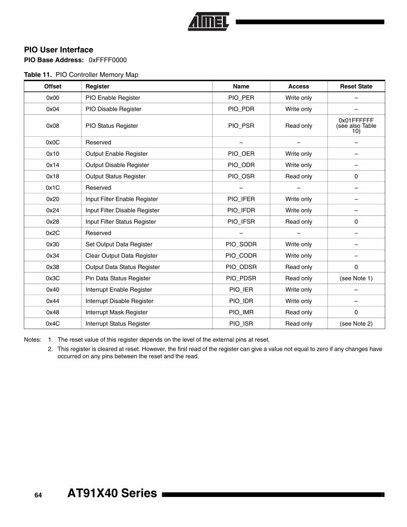
PIO User InterfacePIO Base Address: 0xFFFF0000
Notes: 1. The reset value of this register depends on the level of the external pins at reset.
2. This register is cleared at reset. However, the first read of the register can give a value not equal to zero if any changes have occurred on any pins between the reset and the read.
Table 11. PIO Controller Memory Map
Offset Register Name Access Reset State
0x00 PIO Enable Register PIO_PER Write only –
0x04 PIO Disable Register PIO_PDR Write only –
0x08 PIO Status Register PIO_PSR Read only0x01FFFFFF
(see also Table 10)
0x0C Reserved – – –
0x10 Output Enable Register PIO_OER Write only –
0x14 Output Disable Register PIO_ODR Write only –
0x18 Output Status Register PIO_OSR Read only 0
0x1C Reserved – – –
0x20 Input Filter Enable Register PIO_IFER Write only –
0x24 Input Filter Disable Register PIO_IFDR Write only –
0x28 Input Filter Status Register PIO_IFSR Read only 0
0x2C Reserved – – –
0x30 Set Output Data Register PIO_SODR Write only –
0x34 Clear Output Data Register PIO_CODR Write only –
0x38 Output Data Status Register PIO_ODSR Read only 0
0x3C Pin Data Status Register PIO_PDSR Read only (see Note 1)
0x40 Interrupt Enable Register PIO_IER Write only –
0x44 Interrupt Disable Register PIO_IDR Write only –
0x48 Interrupt Mask Register PIO_IMR Read only 0
0x4C Interrupt Status Register PIO_ISR Read only (see Note 2)
AT91X40 Series64

AT91X40 Series
PIO Enable RegisterRegister Name: PIO_PERAccess Type: Write onlyOffset: 0x00
This register is used to enable individual pins to be controlled by the PIO Controller instead of the associated peripheral.When the PIO is enabled, the associated peripheral input (if any) is held at logic zero.
1 = Enables the PIO to control the corresponding pin (disables peripheral control of the pin).0 = No effect.
PIO Disable RegisterRegister Name: PIO_PDRAccess Type: Write OnlyOffset: 0x04
This register is used to disable PIO control of individual pins. When the PIO control is disabled, the normal peripheral func-tion is enabled on the corresponding pin.
1 = Disables PIO control (enables peripheral control) on the corresponding pin.0 = No effect.
31 30 29 28 27 26 25 24
P31 P30 P29 P28 P27 P26 P25 P24
23 22 21 20 19 18 17 16
P23 P22 P21 P20 P19 P18 P17 P16
15 14 13 12 11 10 9 8
P15 P14 P13 P12 P11 P10 P9 P8
7 6 5 4 3 2 1 0
P7 P6 P5 P4 P3 P2 P1 P0
31 30 29 28 27 26 25 24
P31 P30 P29 P28 P27 P26 P25 P24
23 22 21 20 19 18 17 16
P23 P22 P21 P20 P19 P18 P17 P16
15 14 13 12 11 10 9 8
P15 P14 P13 P12 P11 P10 P9 P8
7 6 5 4 3 2 1 0
P7 P6 P5 P4 P3 P2 P1 P0
65

PIO Status RegisterRegister Name: PIO_PSRAccess Type: Read onlyReset Value: 0x01FFFFFFOffset: 0x08
This register indicates which pins are enabled for PIO control. This register is updated when PIO lines are enabled or dis-abled.
1 = PIO is active on the corresponding line (peripheral is inactive).0 = PIO is inactive on the corresponding line (peripheral is active).
31 30 29 28 27 26 25 24
P31 P30 P29 P28 P27 P26 P25 P24
23 22 21 20 19 18 17 16
P23 P22 P21 P20 P19 P18 P17 P16
15 14 13 12 11 10 9 8
P15 P14 P13 P12 P11 P10 P9 P8
7 6 5 4 3 2 1 0
P7 P6 P5 P4 P3 P2 P1 P0
AT91X40 Series66

AT91X40 Series
PIO Output Enable Register Register Name: PIO_OERAccess Type: Write onlyOffset: 0x10
This register is used to enable PIO output drivers. If the pin is driven by a peripheral, this has no effect on the pin, but theinformation is stored. The register is programmed as follows:
1 = Enables the PIO output on the corresponding pin.0 = No effect.
PIO Output Disable RegisterRegister Name: PIO_ODRAccess Type: Write onlyOffset: 0x14
This register is used to disable PIO output drivers. If the pin is driven by the peripheral, this has no effect on the pin, but theinformation is stored. The register is programmed as follows:
1 = Disables the PIO output on the corresponding pin.0 = No effect.
31 30 29 28 27 26 25 24
P31 P30 P29 P28 P27 P26 P25 P24
23 22 21 20 19 18 17 16
P23 P22 P21 P20 P19 P18 P17 P16
15 14 13 12 11 10 9 8
P15 P14 P13 P12 P11 P10 P9 P8
7 6 5 4 3 2 1 0
P7 P6 P5 P4 P3 P2 P1 P0
31 30 29 28 27 26 25 24
P31 P30 P29 P28 P27 P26 P25 P24
23 22 21 20 19 18 17 16
P23 P22 P21 P20 P19 P18 P17 P16
15 14 13 12 11 10 9 8
P15 P14 P13 P12 P11 P10 P9 P8
7 6 5 4 3 2 1 0
P7 P6 P5 P4 P3 P2 P1 P0
67
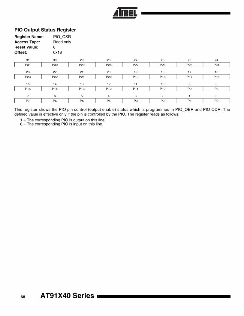
PIO Output Status RegisterRegister Name: PIO_OSRAccess Type: Read onlyReset Value: 0 Offset: 0x18
This register shows the PIO pin control (output enable) status which is programmed in PIO_OER and PIO ODR. Thedefined value is effective only if the pin is controlled by the PIO. The register reads as follows:
1 = The corresponding PIO is output on this line.0 = The corresponding PIO is input on this line.
31 30 29 28 27 26 25 24
P31 P30 P29 P28 P27 P26 P25 P24
23 22 21 20 19 18 17 16
P23 P22 P21 P20 P19 P18 P17 P16
15 14 13 12 11 10 9 8
P15 P14 P13 P12 P11 P10 P9 P8
7 6 5 4 3 2 1 0
P7 P6 P5 P4 P3 P2 P1 P0
AT91X40 Series68

AT91X40 Series
PIO Input Filter Enable RegisterRegister Name: PIO_IFERAccess Type: Write onlyOffset: 0x20
This register is used to enable input glitch filters. It affects the pin whether or not the PIO is enabled. The register is pro-grammed as follows:
1 = Enables the glitch filter on the corresponding pin.0 = No effect.
PIO Input Filter Disable RegisterRegister Name: IO_IFDRAccess Type: Write onlyOffset: 0x24
This register is used to disable input glitch filters. It affects the pin whether or not the PIO is enabled. The register is pro-grammed as follows:
1 = Disables the glitch filter on the corresponding pin.0 = No effect.
31 30 29 28 27 26 25 24
P31 P30 P29 P28 P27 P26 P25 P24
23 22 21 20 19 18 17 16
P23 P22 P21 P20 P19 P18 P17 P16
15 14 13 12 11 10 9 8
P15 P14 P13 P12 P11 P10 P9 P8
7 6 5 4 3 2 1 0
P7 P6 P5 P4 P3 P2 P1 P0
31 30 29 28 27 26 25 24
P31 P30 P29 P28 P27 P26 P25 P24
23 22 21 20 19 18 17 16
P23 P22 P21 P20 P19 P18 P17 P16
15 14 13 12 11 10 9 8
P15 P14 P13 P12 P11 P10 P9 P8
7 6 5 4 3 2 1 0
P7 P6 P5 P4 P3 P2 P1 P0
69

PIO Input Filter Status RegisterRegister Name: PIO_IFSRAccess Type: Read onlyReset Value: 0Offset: 0x28
This register indicates which pins have glitch filters selected. It is updated when PIO outputs are enabled or disabled bywriting to PIO_IFER or PIO_IFDR.
1 = Filter is selected on the corresponding input (peripheral and PIO).0 = Filter is not selected on the corresponding input.
31 30 29 28 27 26 25 24
P31 P30 P29 P28 P27 P26 P25 P24
23 22 21 20 19 18 17 16
P23 P22 P21 P20 P19 P18 P17 P16
15 14 13 12 11 10 9 8
P15 P14 P13 P12 P11 P10 P9 P8
7 6 5 4 3 2 1 0
P7 P6 P5 P4 P3 P2 P1 P0
AT91X40 Series70

AT91X40 Series
PIO Set Output Data RegisterRegister Name: PIO_SODRAccess Type: Write onlyOffset: 0x30
This register is used to set PIO output data. It affects the pin only if the corresponding PIO output line is enabled and if thepin is controlled by the PIO. Otherwise, the information is stored.
1 = PIO output data on the corresponding pin is set.0 = No effect.
PIO Clear Output Data RegisterRegister Name: PIO_CODRAccess Type: Write onlyOffset: 0x34
This register is used to clear PIO output data. It affects the pin only if the corresponding PIO output line is enabled and if thepin is controlled by the PIO. Otherwise, the information is stored.
1 = PIO output data on the corresponding pin is cleared.0 = No effect.
31 30 29 28 27 26 25 24
P31 P30 P29 P28 P27 P26 P25 P24
23 22 21 20 19 18 17 16
P23 P22 P21 P20 P19 P18 P17 P16
15 14 13 12 11 10 9 8
P15 P14 P13 P12 P11 P10 P9 P8
7 6 5 4 3 2 1 0
P7 P6 P5 P4 P3 P2 P1 P0
31 30 29 28 27 26 25 24
P31 P30 P29 P28 P27 P26 P25 P24
23 22 21 20 19 18 17 16
P23 P22 P21 P20 P19 P18 P17 P16
15 14 13 12 11 10 9 8
P15 P14 P13 P12 P11 P10 P9 P8
7 6 5 4 3 2 1 0
P7 P6 P5 P4 P3 P2 P1 P0
71

PIO Output Data Status RegisterRegister Name: PIO_ODSRAccess Type: Read onlyReset Value: 0Offset: 0x38
This register shows the output data status which is programmed in PIO_SODR or PIO_CODR. The defined value is effec-tive only if the pin is controlled by the PIO Controller and only if the pin is defined as an output.
1 = The output data for the corresponding line is programmed to 1.0 = The output data for the corresponding line is programmed to 0.
PIO Pin Data Status RegisterRegister Name: PIO_PDSRAccess Type: Read onlyReset Value: see Table 11Offset: 0x3C
This register shows the state of the physical pin of the chip. The pin values are always valid regardless of whether the pinsare enabled as PIO, peripheral, input or output. The register reads as follows:
1 = The corresponding pin is at logic 1.0 = The corresponding pin is at logic 0.
31 30 29 28 27 26 25 24
P31 P30 P29 P28 P27 P26 P25 P24
23 22 21 20 19 18 17 16
P23 P22 P21 P20 P19 P18 P17 P16
15 14 13 12 11 10 9 8
P15 P14 P13 P12 P11 P10 P9 P8
7 6 5 4 3 2 1 0
P7 P6 P5 P4 P3 P2 P1 P0
31 30 29 28 27 26 25 24
P31 P30 P29 P28 P27 P26 P25 P24
23 22 21 20 19 18 17 16
P23 P22 P21 P20 P19 P18 P17 P16
15 14 13 12 11 10 9 8
P15 P14 P13 P12 P11 P10 P9 P8
7 6 5 4 3 2 1 0
P7 P6 P5 P4 P3 P2 P1 P0
AT91X40 Series72

AT91X40 Series
PIO Interrupt Enable RegisterRegister Name: PIO_IERAccess Type: Write onlyOffset: 0x40
This register is used to enable PIO interrupts on the corresponding pin. It has effect whether PIO is enabled or not.
1 = Enables an interrupt when a change of logic level is detected on the corresponding pin.0 = No effect.
PIO Interrupt Disable RegisterRegister Name: PIO_IDRAccess Type: Write onlyOffset: 0x44
This register is used to disable PIO interrupts on the corresponding pin. It has effect whether the PIO is enabled or not.
1 = Disables the interrupt on the corresponding pin. Logic level changes are still detected.0 = No effect.
31 30 29 28 27 26 25 24
P31 P30 P29 P28 P27 P26 P25 P24
23 22 21 20 19 18 17 16
P23 P22 P21 P20 P19 P18 P17 P16
15 14 13 12 11 10 9 8
P15 P14 P13 P12 P11 P10 P9 P8
7 6 5 4 3 2 1 0
P7 P6 P5 P4 P3 P2 P1 P0
31 30 29 28 27 26 25 24
P31 P30 P29 P28 P27 P26 P25 P24
23 22 21 20 19 18 17 16
P23 P22 P21 P20 P19 P18 P17 P16
15 14 13 12 11 10 9 8
P15 P14 P13 P12 P11 P10 P9 P8
7 6 5 4 3 2 1 0
P7 P6 P5 P4 P3 P2 P1 P0
73
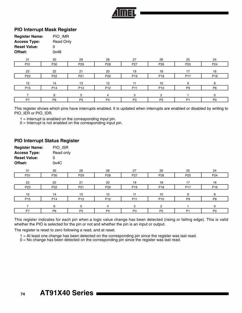
PIO Interrupt Mask RegisterRegister Name: PIO_IMRAccess Type: Read OnlyReset Value: 0Offset: 0x48
This register shows which pins have interrupts enabled. It is updated when interrupts are enabled or disabled by writing toPIO_IER or PIO_IDR.
1 = Interrupt is enabled on the corresponding input pin.0 = Interrupt is not enabled on the corresponding input pin.
PIO Interrupt Status RegisterRegister Name: PIO_ISRAccess Type: Read onlyReset Value: 0Offset: 0x4C
This register indicates for each pin when a logic value change has been detected (rising or falling edge). This is validwhether the PIO is selected for the pin or not and whether the pin is an input or output.
The register is reset to zero following a read, and at reset.
1 = At least one change has been detected on the corresponding pin since the register was last read.0 = No change has been detected on the corresponding pin since the register was last read.
31 30 29 28 27 26 25 24
P31 P30 P29 P28 P27 P26 P25 P24
23 22 21 20 19 18 17 16
P23 P22 P21 P20 P19 P18 P17 P16
15 14 13 12 11 10 9 8
P15 P14 P13 P12 P11 P10 P9 P8
7 6 5 4 3 2 1 0
P7 P6 P5 P4 P3 P2 P1 P0
31 30 29 28 27 26 25 24
P31 P30 P29 P28 P27 P26 P25 P24
23 22 21 20 19 18 17 16
P23 P22 P21 P20 P19 P18 P17 P16
15 14 13 12 11 10 9 8
P15 P14 P13 P12 P11 P10 P9 P8
7 6 5 4 3 2 1 0
P7 P6 P5 P4 P3 P2 P1 P0
AT91X40 Series74

AT91X40 Series
WD: Watchdog TimerThe AT91X40 Series has an internal watchdog timer whichcan be used to prevent system lock-up if the softwarebecomes trapped in a deadlock. In normal operation theuser reloads the watchdog at regular intervals before thetimer overflow occurs. If an overflow does occur, the watch-dog timer generates one or a combination of the followingsignals, depending on the parameters in WD_OMR (Over-flow Mode Register):• If RSTEN is set, an internal reset is generated
(WD_RESET as shown in Figure 35).
• If IRQEN is set, a pulse is generated on the signal WDIRQ which is connected to the Advanced Interrupt Controller
• If EXTEN is set, a low level is driven on the NWDOVF signal for a duration of 8 MCK cycles.
The watchdog timer has a 16-bit down counter. Bits 12-15of the value loaded when the watchdog is restarted are pro-grammable using the HPVC parameter in WD_CMR (ClockMode). Four clock sources are available to the watchdogcounter: MCK/8, MCK/32, MCK/128 or MCK/1024. Theselection is made using the WDCLKS parameter inWD_CMR. This provides a programmable time-out periodof 1 ms to 2 sec. with a 33 MHz system clock.
All write accesses are protected by control access keys tohelp prevent corruption of the watchdog should an errorcondition occur. To update the contents of the mode andcontrol registers it is necessary to write the correct bit pat-tern to the control access key bits at the same time as thecontrol bits are written (the same write access).
Figure 35. Watchdog Timer Block Diagram
WD User InterfaceWD Base Address: 0xFFFF8000
Table 12. WD Memory Map
Offset Register Name Access Reset State
0x00 Overflow Mode Register WD_OMR Read/Write 0
0x04 Clock Mode Register WD_CMR Read/Write 0
0x08 Control Register WD_CR Write only –
0x0C Status Register WD_SR Read only 0
Advanced PeripheralBus (APB)
WD_RESET
WDIRQ
MCKI/8
MCKI/32
MCKI/128
MCKI/1024
Control Logic
Clock Select16-Bit
ProgrammableDown CounterCLK_CNT
Clear
Overflow
NWDOVF
75

WD Overflow Mode RegisterName: WD_OMRAccess: Read/WriteReset Value: 0Offset: 0x00
• WDEN: Watch Dog Enable0 = Watch Dog is disabled and does not generate any signals.1 = Watch Dog is enabled and generates enabled signals.
• RSTEN: Reset Enable0 = Generation of an internal reset by the Watch Dog is disabled.1 = When overflow occurs, the Watch Dog generates an internal reset.
• IRQEN: Interrupt Enable0 = Generation of an interrupt by the Watch Dog is disabled.1 = When overflow occurs, the Watch Dog generates an interrupt.
• EXTEN: External Signal Enable0 = Generation of a pulse on the pin NWDOVF by the Watch Dog is disabled.1 = When an overflow occurs, a pulse on the pin NWDOVF is generated.
• OKEY: Overflow Access KeyUsed only when writing WD_OMR. OKEY is read as 0.0x234 = Write access in WD_OMR is allowed.Other value = Write access in WD_OMR is prohibited.
31 30 29 28 27 26 25 24
– – – – – – – –
23 22 21 20 19 18 17 16
– – – – – – – –
15 14 13 12 11 10 9 8
OKEY
7 6 5 4 3 2 1 0
OKEY EXTEN IRQEN RSTEN WDEN
AT91X40 Series76
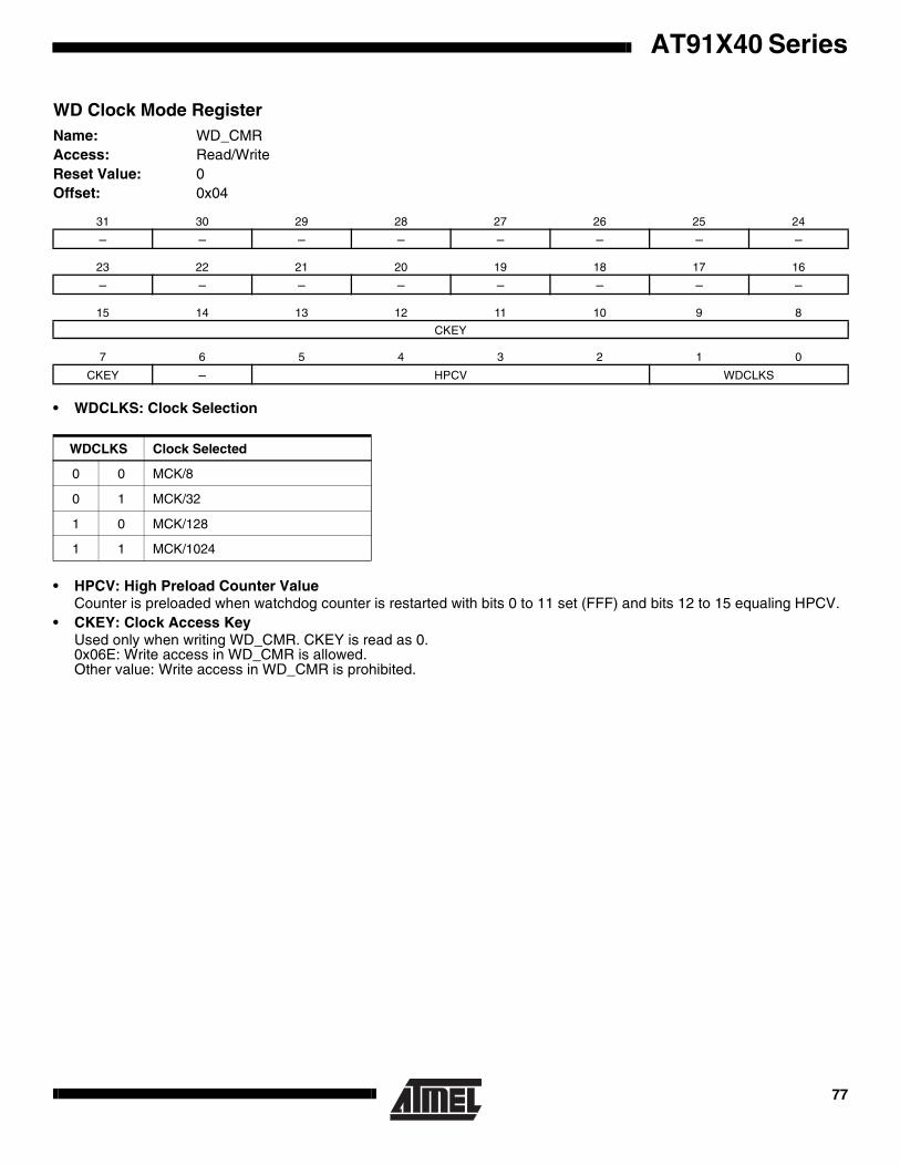
AT91X40 Series
WD Clock Mode RegisterName: WD_CMRAccess: Read/WriteReset Value: 0Offset: 0x04
• WDCLKS: Clock Selection
• HPCV: High Preload Counter ValueCounter is preloaded when watchdog counter is restarted with bits 0 to 11 set (FFF) and bits 12 to 15 equaling HPCV.
• CKEY: Clock Access KeyUsed only when writing WD_CMR. CKEY is read as 0.0x06E: Write access in WD_CMR is allowed.Other value: Write access in WD_CMR is prohibited.
31 30 29 28 27 26 25 24
– – – – – – – –
23 22 21 20 19 18 17 16
– – – – – – – –
15 14 13 12 11 10 9 8
CKEY
7 6 5 4 3 2 1 0
CKEY – HPCV WDCLKS
WDCLKS Clock Selected
0 0 MCK/8
0 1 MCK/32
1 0 MCK/128
1 1 MCK/1024
77
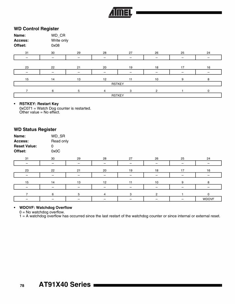
WD Control RegisterName: WD_CRAccess: Write only Offset: 0x08
• RSTKEY: Restart Key0xC071 = Watch Dog counter is restarted.Other value = No effect.
WD Status RegisterName: WD_SRAccess: Read onlyReset Value: 0Offset: 0x0C
• WDOVF: Watchdog Overflow0 = No watchdog overflow.1 = A watchdog overflow has occurred since the last restart of the watchdog counter or since internal or external reset.
31 30 29 28 27 26 25 24
– – – – – – – –
23 22 21 20 19 18 17 16
– – – – – – – –
15 14 13 12 11 10 9 8
RSTKEY
7 6 5 4 3 2 1 0
RSTKEY
31 30 29 28 27 26 25 24
– – – – – – – –
23 22 21 20 19 18 17 16
– – – – – – – –
15 14 13 12 11 10 9 8
– – – – – – – –
7 6 5 4 3 2 1 0
– – – – – – – WDOVF
AT91X40 Series78
AT91X40 Series
WD Enabling SequenceTo enable the Watchdog Timer the sequence is as follows:
1. Disable the Watchdog by clearing the bit WDEN:
Write 0x2340 to WD_OMR
This step is unnecessary if the WD is already disabled(reset state).
2. Initialize the WD Clock Mode Register:
Write 0x373C to WD_CMR (HPCV = 15 and WDCLKS = MCK/8)
3. Restart the timer:
Write 0xC071 to WD_CR
4. Enable the watchdog:
Write 0x2345 to WD_OMR (interrupt enabled)
79
SF: Special Function RegistersThe AT91X40 Series provides registers which implement the following special functions.
• Chip identification• RESET status• Protect Mode (see Protect Mode on page 48)
Chip IdentificationTable 13 provides the Chip ID values for the products described in this datasheet.
SF User InterfaceChip ID Base Address = 0xFFF00000
Table 13. Chip ID Values
Product Chip
AT91M40800 0x14080044
AT91R40807 0x44080746
AT91M40807 0x014080745
Table 14. SF Memory Map
Offset Register Name Access Reset State
0x00 Chip ID Register SF_CIDR Read only Hardwired
0x04 Chip ID Extension Register SF_EXID Read only Hardwired
0x08 Reset Status Register SF_RSR Read only See register description
0x0C Memory Mode Register SF_MMR Read/Write 0x0
0x10 Reserved – – –
0x14 Reserved – – –
0x18 Protect Mode Register SF_PMR Read/Write 0x0
AT91X40 Series80

AT91X40 Series
Chip ID RegisterRegister Name: SF_CIDRAccess Type: Read onlyReset Value: HardwiredOffset: 0x00
• VERSION: Version of the chipThis value is incremented by one with each new version of the chip (from zero to a maximum value of 31).
• NVPSIZ: Non Volatile Program Memory Size
• NVDSIZ: Non Volatile Data Memory Size
• VDSIZ: Volatile Data Memory Size
31 30 29 28 27 26 25 24
EXT NVPTYP ARCH
23 22 21 20 19 18 17 16
ARCH VDSIZ
15 14 13 12 11 10 9 8
NVDSIZ NVPSIZ
7 6 5 4 3 2 1 0
0 1 0 VERSION
NVPSIZ Size
0 0 0 0 None
0 0 1 1 32K bytes
0 1 0 1 64K bytes
0 1 1 1 128K bytes
1 0 0 1 256K bytes
Others Reserved
NVDSIZ Size
0 0 0 0 None
Others Reserved
VDSIZ Size
0 0 0 0 None
0 0 0 1 1K bytes
0 0 1 0 2K bytes
0 1 0 0 4K bytes
1 0 0 0 8K bytes
Others Reserved
81
• ARCH: Chip ArchitectureCode of Architecture: Two BCD digits.
• NVPTYP: Non Volatile Program Memory Type
• EXT: Extension Flag0 = Chip ID has a single register definition without extensions1 = An extended Chip ID exists (to be defined in the future).
Chip ID Extension Register Register Name: SF_EXIDAccess Type: Read onlyReset Value: HardwiredOffset: 0x04
This register is reserved for future use. It will be defined when needed.
0100 0000 AT91x40yyy
NVPTYP Type
0 0 0 Reserved
0 0 1 “F” Series
1 x x Reserved
1 0 0 “R” Series
AT91X40 Series82

AT91X40 Series
Reset Status RegisterRegister Name: SF_RSRAccess Type: Read onlyReset Value: See belowOffset: 0x08
• RESET: Reset Status InformationThis field indicates whether the reset was demanded by the external system (via NRST) or by the Watchdog internalreset request.
31 30 29 28 27 26 25 24
– – – – – – – –
23 22 21 20 19 18 17 16
– – – – – – – –
15 14 13 12 11 10 9 8
– – – – – – – –
7 6 5 4 3 2 1 0
RESET
Reset Cause of Reset
0x6C External Pin
0x53 Internal Watchdog
83
SF Memory Mode Register This register only applies to the AT91R40807.Register Name: SF_MMRAccess Type: Read/WriteReset Value: 0Offset: 0x0C
• RAMWU: Internal Extended RAM Write Detection0 = Writing in RAM generates an Abort.1 = Writing in RAM is allowed.
SF Protect Mode RegisterRegister Name: SF_PMRAccess Type: Read/WriteReset Value: 0Offset: 0x18
• PMRKEY: Protect Mode Register KeyUsed only when writing SF_PMR. PMRKEY is reads 0.0x27A8: Write access in SF_PMR is allowed.Other value: Write access in SF_PMR is prohibited.
• AIC: AIC Protect Mode Enable0 = The Advanced Interrupt Controller runs in Normal Mode.1 = The Advanced Interrupt Controller runs in Protect Mode.See Protect Mode on page 48.
31 30 29 28 27 26 25 24
– – – – – – – –
23 22 21 20 19 18 17 16
– – – – – – – –
15 14 13 12 11 10 9 8
– – – – – – – –
7 6 5 4 3 2 1 0
– – – – – – – RAMWU
31 30 29 28 27 26 25 24
PMRKEY
23 22 21 20 19 18 17 16
PMRKEY
15 14 13 12 11 10 9 8
– – – – – – – –
7 6 5 4 3 2 1 0
– – AIC – – – – –
AT91X40 Series84

AT91X40 Series
USART: Universal Synchronous/Asynchronous Receiver/TransmitterThe AT91X40 Series provides two identical, full-duplex,universal synchronous/asynchronous receiver/transmittersthat interface to the APB and are connected to the Periph-eral Data Controller.
The main features are:• Programmable Baud Rate Generator
• Parity, Framing and Overrun Error Detection
• Line Break Generation and Detection
• Automatic Echo, Local Loopback and Remote Loopback channel modes
• Multi-drop Mode: Address Detection and Generation
• Interrupt Generation
• Two Dedicated Peripheral Data Controller channels
• 5-, 6-, 7-, 8- and 9-bit character length
Figure 36. USART Block Diagram
Pin DescriptionEach USART channel has the following external signals:
Notes: 1. After a hardware reset, the USART pins are not enabled by default (see PIO: Parallel I/O Controller on page 61). The user must configure the PIO Con-troller before enabling the transmitter or receiver.
2. If the user selects one of the internal clocks, SCK can be configured as a PIO.
Peripheral Data Controller
ReceiverChannel
TransmitterChannel
Control Logic
Interrupt Control
Baud Rate Generator
Receiver
Transmitter
AMBA
ASB
APB
USxIRQ
MCK
MCK/8
RXD
TXD
SCK
USART Channel
Baud Rate Clock
PIO: Parallel
I/O Controller
Name Description
SCKUSART Serial clock can be configured as input or output:SCK is configured as input if an External clock is selected (USCLKS[1] = 1)SCK is driven as output if the External Clock is disabled (USCLKS[1] = 0) and Clock output is enabled (CLKO = 1)
TXD Transmit Serial Data is an output
RXD Receive Serial Data is an input
85
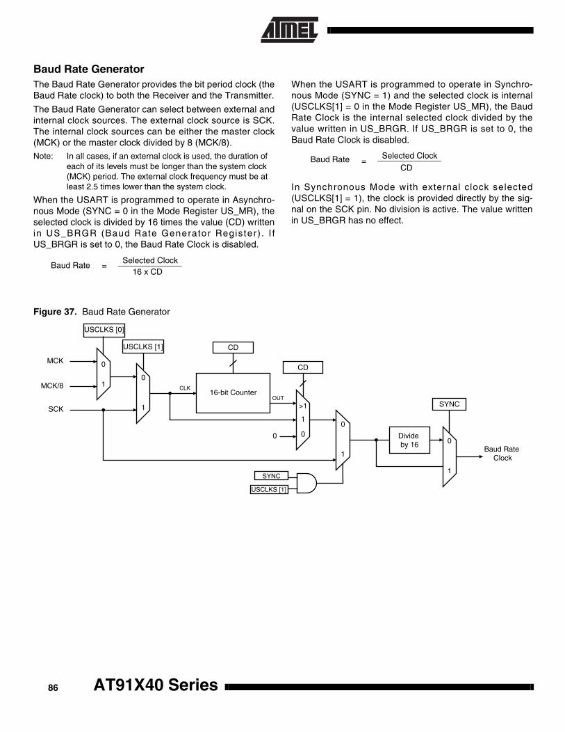
Baud Rate Generator The Baud Rate Generator provides the bit period clock (theBaud Rate clock) to both the Receiver and the Transmitter.
The Baud Rate Generator can select between external andinternal clock sources. The external clock source is SCK.The internal clock sources can be either the master clock(MCK) or the master clock divided by 8 (MCK/8).Note: In all cases, if an external clock is used, the duration of
each of its levels must be longer than the system clock (MCK) period. The external clock frequency must be at least 2.5 times lower than the system clock.
When the USART is programmed to operate in Asynchro-nous Mode (SYNC = 0 in the Mode Register US_MR), theselected clock is divided by 16 times the value (CD) writtenin US_BRGR (Baud Rate Generator Register) . I fUS_BRGR is set to 0, the Baud Rate Clock is disabled.
When the USART is programmed to operate in Synchro-nous Mode (SYNC = 1) and the selected clock is internal(USCLKS[1] = 0 in the Mode Register US_MR), the BaudRate Clock is the internal selected clock divided by thevalue written in US_BRGR. If US_BRGR is set to 0, theBaud Rate Clock is disabled.
In Synchronous Mode with external clock selected(USCLKS[1] = 1), the clock is provided directly by the sig-nal on the SCK pin. No division is active. The value writtenin US_BRGR has no effect.
Figure 37. Baud Rate Generator
Baud Rate =Selected Clock
16 x CD
Baud Rate =Selected Clock
CD
USCLKS [1]
0
01
1
MCK
MCK/8
SCK
CLK16-bit Counter
0
0
1Baud Rate
Clock
SYNC
USCLKS [1]
CD
CD
OUT
0
1
Divide by 16
SYNC
0
1
>1
USCLKS [0]
AT91X40 Series86
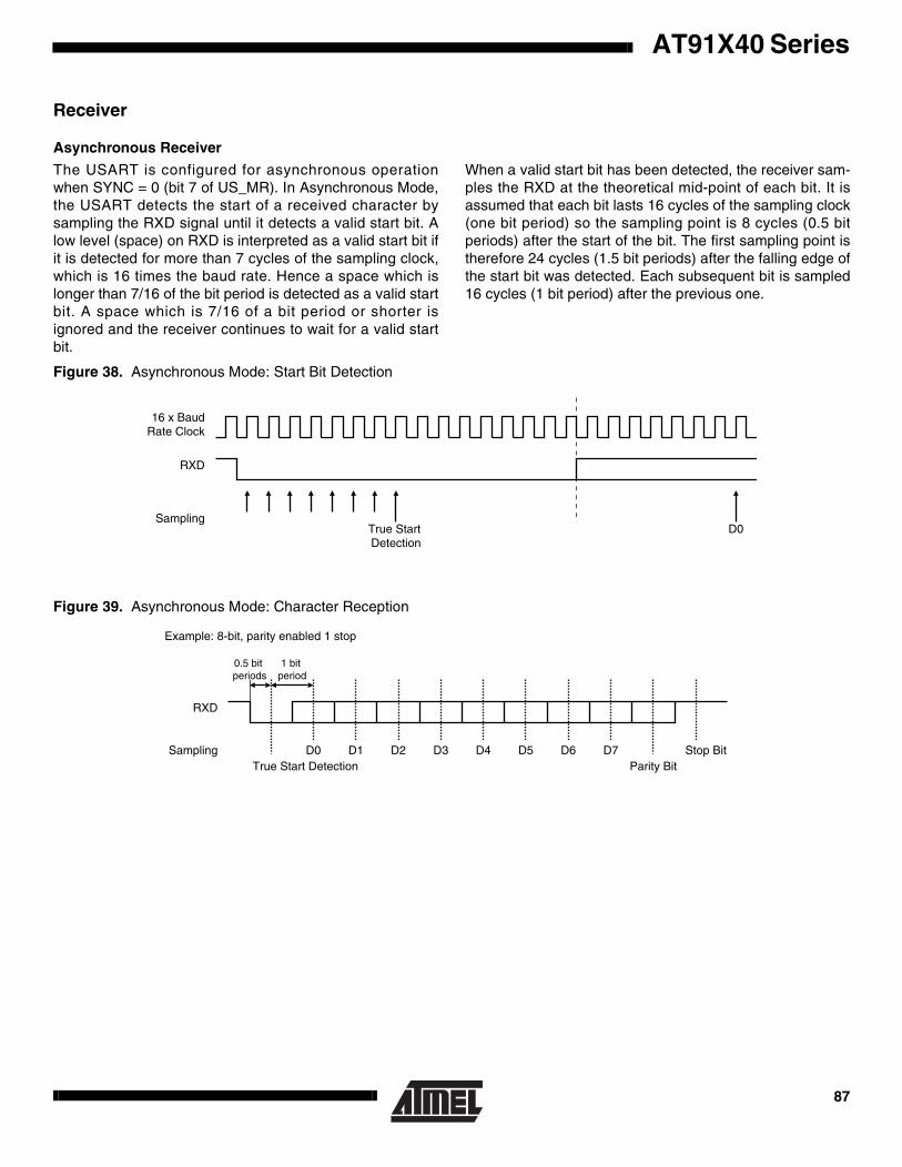
AT91X40 Series
Receiver
Asynchronous Receiver
The USART is configured for asynchronous operationwhen SYNC = 0 (bit 7 of US_MR). In Asynchronous Mode,the USART detects the start of a received character bysampling the RXD signal until it detects a valid start bit. Alow level (space) on RXD is interpreted as a valid start bit ifit is detected for more than 7 cycles of the sampling clock,which is 16 times the baud rate. Hence a space which islonger than 7/16 of the bit period is detected as a valid startbit. A space which is 7/16 of a bit period or shorter isignored and the receiver continues to wait for a valid startbit.
When a valid start bit has been detected, the receiver sam-ples the RXD at the theoretical mid-point of each bit. It isassumed that each bit lasts 16 cycles of the sampling clock(one bit period) so the sampling point is 8 cycles (0.5 bitperiods) after the start of the bit. The first sampling point istherefore 24 cycles (1.5 bit periods) after the falling edge ofthe start bit was detected. Each subsequent bit is sampled16 cycles (1 bit period) after the previous one.
Figure 38. Asynchronous Mode: Start Bit Detection
Figure 39. Asynchronous Mode: Character Reception
16 x BaudRate Clock
RXD
True Start Detection
D0Sampling
D0 D1 D2 D3 D4 D5 D6 D7
RXD
True Start DetectionSampling
Parity BitStop Bit
Example: 8-bit, parity enabled 1 stop
1 bit period
0.5 bit periods
87

Synchronous Receiver
When configured for synchronous operation (SYNC = 1),the receiver samples the RXD signal on each rising edge ofthe Baud Rate clock. If a low level is detected, it is consid-
ered as a start. Data bits, parity bit and stop bit are sampledand the receiver waits for the next start bit. See example inFigure 40.
Figure 40. Synchronous Mode: Character Reception
Receiver Ready
When a complete character is received, it is transferred tothe US_RHR and the RXRDY status bit in US_CSR is set.If US_RHR has not been read since the last transfer, theOVRE status bit in US_CSR is set.
Parity Error
Each time a character is received, the receiver calculatesthe parity of the received data bits, in accordance with thefield PAR in US_MR. It then compares the result with thereceived parity bit. If different, the parity error bit PARE inUS_CSR is set.
Framing Error
If a character is received with a stop bit at low level andwith at least one data bit at high level, a framing error isgenerated. This sets FRAME in US_CSR.
Time-out
This function allows an idle condition on the RXD line to bedetected. The maximum delay for which the USART shouldwait for a new character to arrive while the RXD line is inac-tive (high level) is programmed in US_RTOR (ReceiverTime-out). When this register is set to 0, no time-out isdetected. Otherwise, the receiver waits for a first characterand then initializes a counter which is decremented at eachbit period and reloaded at each byte reception. When thecounter reaches 0, the TIMEOUT bit in US_CSR is set. Theuser can restart the wait for a first character with theSTTTO (Start Time-out) bit in US_CR.
Calculation of time-out duration:
D0 D1 D2 D3 D4 D5 D6 D7
RXD
True Start DetectionSampling
Parity BitStop Bit
Example: 8-bit, parity enabled 1 stop
SCK
Duration = Value x 4 x Bit period
AT91X40 Series88

AT91X40 Series
TransmitterThe transmitter has the same behavior in both synchronousand asynchronous operating modes. Start bit, data bits,parity bit and stop bits are serially shifted, lowest significantbit first, on the falling edge of the serial clock. See examplein Figure 41.
The number of data bits is selected in the CHRL field inUS_MR.
The parity bit is set according to the PAR field in US_MR.
The number of stop bits is selected in the NBSTOP field inUS_MR.
When a character is written to US_THR (Transmit Holding),it is transferred to the Shift Register as soon as it is empty.When the transfer occurs, the TXRDY bit in US_CSR is setuntil a new character is written to US_THR. If Transmit ShiftRegister and US_THR are both empty, the TXEMPTY bit inUS_CSR is set.
Time-guard
The Time-guard function allows the transmitter to insert anidle state on the TXD line between two characters. Theduration of the idle state is programmed in US_TTGR
(Transmitter Time-guard). When this register is set to zero,no time-guard is generated. Otherwise, the transmitterholds a high level on TXD after each transmitted byte dur-ing the number of bit periods programmed in US_TTGR
Multi-drop Mode
When the field PAR in US_MR equals 11X (binary value),the USART is configured to run in Multi-drop Mode. In thiscase, the parity error bit PARE in US_CSR is set when datais detected with a parity bit set to identify an address byte.PARE is cleared with the Reset Status Bits Command(RSTSTA) in US_CR. If the parity bit is detected low, identi-fying a data byte, PARE is not set.
The transmitter sends an address byte (parity bit set) whena Send Address Command (SENDA) is written to US_CR.In this case, the next byte written to US_THR will be trans-mitted as an address. After this any byte transmitted willhave the parity bit cleared.
Figure 41. Synchronous and Asynchronous Modes: Character Transmission
Idle state durationbetween two characters = Time-guard
Value x BitPeriod
D0 D1 D2 D3 D4 D5 D6 D7
TXD
Start Bit
ParityBit
StopBit
Example: 8-bit, parity enabled 1 stop
Baud Rate Clock
89

Break A break condition is a low signal level which has a durationof at least one character (including start/stop bits andparity).
Transmit Break
The transmitter generates a break condition on the TXDline when STTBRK is set in US_CR (Control Register). Inthis case, the character present in the Transmit Shift Regis-ter is completed before the line is held low.
To cancel a break condition on the TXD line, the STPBRKcommand in US_CR must be set. The USART completes aminimum break duration of one character length. The TXDline then returns to high level (idle state) for at least 12 bitperiods to ensure that the end of break is correctlydetected. Then the transmitter resumes normal operation.
The BREAK is managed like a character:• The STTBRK and the STPBRK commands are
performed only if the transmitter is ready (bit TXRDY = 1 in US_CSR)
• The STTBRK command blocks the transmitter holding register (bit TXRDY is cleared in US_CSR) until the break has started
• A break is started when the Shift Register is empty (any previous character is fully transmitted). TXEMPTY is cleared in US_CSR. The break blocks the transmitter shift register until it is completed (high level for at least 12 bit periods after the STPBRK command is requested)
In order to avoid unpredictable states:• STTBRK and STPBRK commands must not be
requested at the same time
• Once an STTBRK command is requested, further STTBRK commands are ignored until the BREAK is ended (high level for at least 12 bit periods)
• All STPBRK commands requested without a previous STTBRK command are ignored
• A byte written into the Transmit Holding Register while a break is pending but not started (US_CSR.TXRDY = 0) is ignored
• It is not permitted to write new data in the Transmit Holding Register while a break is in progress (STPBRK has not been requested), even though TXRDY = 1 in US_CSR.
• A new STTBRK command must not be issued until an existing break has ended (TXEMPTY = 1 in US_CSR)
The standard break transmission sequence is:
1. Wait for the transmitter ready (US_CSR.TXRDY = 1)
2. Send the STTBRK command(write 0x0200 to US_CR)
3. Wait for the transmitter ready(TXRDY = 1 in US_CSR)
4. Send the STPBRK command(write 0x0400 to US_CR)
The next byte can then be sent:
5. Wait for the transmitter ready(TXRDY = 1 in US_CSR)
6. Send the next byte(write byte to US_THR)
Each of these steps can be scheduled by using the inter-rupt if the bit TXRDY in US_IMR is set.
For character transmission, the USART channel must beenabled before sending a break.
Receive Break
The receiver detects a break condition when all data, parityand stop bits are low. When the low stop bit is detected, thereceiver asserts the RXBRK bit in US_CSR. An end ofreceive break is detected by a high level for at least 2/16 ofa bit period in Asynchronous Mode or at least one samplein Synchronous Mode. RXBRK is also asserted when anend of break is detected.
Both the beginning and the end of a break can be detectedby interrupt if the bit US_IMR.RXBRK is set.
Peripheral Data ControllerEach USART channel is closely connected to a corre-sponding Peripheral Data Controller channel. One isdedicated to the receiver. The other is dedicated to thetransmitter.
Note: The PDC is disabled if 9-bit character length is selected (MODE9 = 1) in US_MR.
The PDC channel is programmed using US_TPR (TransmitPointer) and US_TCR (Transmit Counter) for the transmit-ter and US_RPR (Receive Pointer) and US_RCR (ReceiveCounter) for the receiver. The status of the PDC is given inUS_CSR by the ENDTX bit for the transmitter and by theENDRX bit for the receiver.
The pointer registers (US_TPR and US_RPR) are used tostore the address of the transmit or receive buffers. Thecounter registers (US_TCR and US_RCR) are used tostore the size of these buffers.
The receiver data transfer is triggered by the RXRDY bitand the transmitter data transfer is triggered by TXRDY.When a transfer is performed, the counter is decrementedand the pointer is incremented. When the counter reaches0, the status bit is set (ENDRX for the receiver, ENDTX forthe transmitter in US_CSR) which can be programmed to
AT91X40 Series90
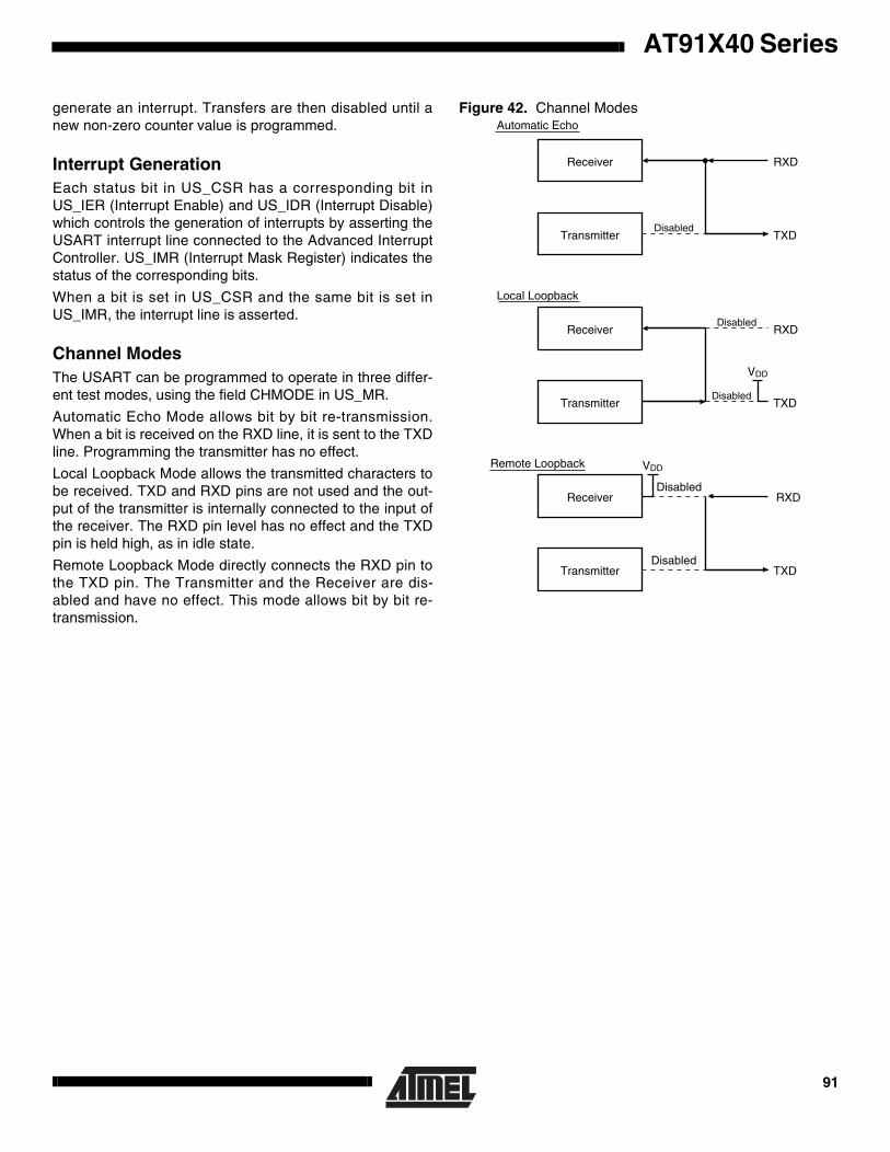
AT91X40 Series
generate an interrupt. Transfers are then disabled until anew non-zero counter value is programmed.
Interrupt GenerationEach status bit in US_CSR has a corresponding bit inUS_IER (Interrupt Enable) and US_IDR (Interrupt Disable)which controls the generation of interrupts by asserting theUSART interrupt line connected to the Advanced InterruptController. US_IMR (Interrupt Mask Register) indicates thestatus of the corresponding bits.
When a bit is set in US_CSR and the same bit is set inUS_IMR, the interrupt line is asserted.
Channel ModesThe USART can be programmed to operate in three differ-ent test modes, using the field CHMODE in US_MR.
Automatic Echo Mode allows bit by bit re-transmission.When a bit is received on the RXD line, it is sent to the TXDline. Programming the transmitter has no effect.
Local Loopback Mode allows the transmitted characters tobe received. TXD and RXD pins are not used and the out-put of the transmitter is internally connected to the input ofthe receiver. The RXD pin level has no effect and the TXDpin is held high, as in idle state.
Remote Loopback Mode directly connects the RXD pin tothe TXD pin. The Transmitter and the Receiver are dis-abled and have no effect. This mode allows bit by bit re-transmission.
Figure 42. Channel Modes
Receiver
TransmitterDisabled
RXD
TXD
Receiver
TransmitterDisabled
RXD
TXD
VDD
Disabled
Receiver
TransmitterDisabled
RXD
TXD
Disabled
Automatic Echo
Local Loopback
Remote Loopback VDD
91

USART User InterfaceBase Address USART0: 0xFFFD0000Base Address USART1: 0xFFFCC000
Table 15. USART Memory Map
Offset Register Name Access Reset State
0x00 Control Register US_CR Write only –
0x04 Mode Register US_MR Read/Write 0
0x08 Interrupt Enable Register US_IER Write only –
0x0C Interrupt Disable Register US_IDR Write only –
0x10 Interrupt Mask Register US_IMR Read only 0
0x14 Channel Status Register US_CSR Read only 0x18
0x18 Receiver Holding Register US_RHR Read only 0
0x1C Transmitter Holding Register US_THR Write only –
0x20 Baud Rate Generator Register US_BRGR Read/Write 0
0x24 Receiver Time-out Register US_RTOR Read/Write 0
0x28 Transmitter Time-guard Register US_TTGR Read/Write 0
0x2C Reserved – – –
0x30 Receive Pointer Register US_RPR Read/Write 0
0x34 Receive Counter Register US_RCR Read/Write 0
0x38 Transmit Pointer Register US_TPR Read/Write 0
0x3C Transmit Counter Register US_TCR Read/Write 0
AT91X40 Series92

AT91X40 Series
USART Control RegisterName: US_CRAccess Type: Write onlyOffset: 0x00
• RSTRX: Reset Receiver0 = No effect.1 = The receiver logic is reset.
• RSTTX: Reset Transmitter0 = No effect.1 = The transmitter logic is reset.
• RXEN: Receiver Enable0 = No effect.1 = The receiver is enabled if RXDIS is 0.
• RXDIS: Receiver Disable0 = No effect.1 = The receiver is disabled.
• TXEN: Transmitter Enable0 = No effect.1 = The transmitter is enabled if TXDIS is 0.
• TXDIS: Transmitter Disable0 = No effect. 1 = The transmitter is disabled.
• RSTSTA: Reset Status Bits0 = No effect.1 = Resets the status bits PARE, FRAME, OVRE and RXBRK in the US_CSR.
• STTBRK: Start Break0 = No effect.1 = If break is not being transmitted, start transmission of a break after the characters present in US_THR and theTransmit Shift Register have been transmitted.
• STPBRK: Stop Break0 = No effect.1 = If a break is being transmitted, stop transmission of the break after a minimum of one character length and transmita high level during 12 bit periods.
• STTTO: Start Time-out0 = No effect.1 = Start waiting for a character before clocking the time-out counter.
• SENDA: Send Address0 = No effect.1 = In Multi-drop Mode only, the next character written to the US_THR is sent with the address bit set.
31 30 29 28 27 26 25 24
– – – – – – – –
23 22 21 20 19 18 17 16
– – – – – – – –
15 14 13 12 11 10 9 8
– – – SENDA STTTO STPBRK STTBRK RSTSTA
7 6 5 4 3 2 1 0
TXDIS TXEN RXDIS RXEN RSTTX RSTRX – –
93

USART Mode RegisterName: US_MRAccess Type: Read/WriteReset Value: 0Offset: 0x04
• USCLKS: Clock Selection (Baud Rate Generator Input Clock)
• CHRL: Character Length
Start, stop and parity bits are added to the character length.• SYNC: Synchronous Mode Select
0 = USART operates in Asynchronous Mode.1 = USART operates in Synchronous Mode.
• PAR: Parity Type
31 30 29 28 27 26 25 24
– – – – – – – –
23 22 21 20 19 18 17 16
– – – – – CLKO MODE9 –
15 14 13 12 11 10 9 8
CHMODE NBSTOP PAR SYNC
7 6 5 4 3 2 1 0
CHRL USCLKS – – – –
USCLKS Selected Clock
0 0 MCK
0 1 MCK/8
1 X External (SCK)
CHRL Character Length
0 0 Five Bits
0 1 Six Bits
1 0 Seven Bits
1 1 Eight Bits
PAR Parity Type
0 0 0 Even Parity
0 0 1 Odd Parity
0 1 0 Parity Forced to 0 (Space)
0 1 1 Parity Forced to 1 (Mark)
1 0 x No Parity
1 1 x Multi-drop Mode
AT91X40 Series94
AT91X40 Series
• NBSTOP: Number of Stop BitsThe interpretation of the number of stop bits depends on SYNC.
• CHMODE: Channel Mode
• MODE9: 9-bit Character Length0 = CHRL defines character length.1 = 9-bit character length.
• CKLO: Clock Output Select0 = The USART does not drive the SCK pin.1 = The USART drives the SCK pin if USCLKS[1] is 0.
NBSTOP Asynchronous (SYNC = 0) Synchronous (SYNC = 1)
0 0 1 Stop Bit 1 Stop Bit
0 1 1.5 Stop Bits Reserved
1 0 2 Stop Bits 2 Stop Bits
1 1 Reserved Reserved
CHMODE Mode Description
0 0 Normal ModeThe USART Channel operates as an Rx/Tx USART.
0 1 Automatic EchoReceiver Data Input is connected to the TXD pin.
1 0 Local LoopbackTransmitter Output Signal is connected to Receiver Input Signal.
1 1 Remote LoopbackRXD pin is internally connected to TXD pin.
95

USART Interrupt Enable RegisterName: US_IERAccess Type: Write onlyOffset: 0x08
• RXRDY: Enable RXRDY Interrupt0 = No effect.1 = Enables RXRDY Interrupt.
• TXRDY: Enable TXRDY Interrupt0 = No effect.1 = Enables TXRDY Interrupt.
• RXBRK: Enable Receiver Break Interrupt0 = No effect.1 = Enables Receiver Break Interrupt.
• ENDRX: Enable End of Receive Transfer Interrupt0 = No effect.1 = Enables End of Receive Transfer Interrupt.
• ENDTX: Enable End of Transmit Interrupt0 = No effect.1 = Enables End of Transmit Interrupt.
• OVRE: Enable Overrun Error Interrupt0 = No effect.1 = Enables Overrun Error Interrupt.
• FRAME: Enable Framing Error Interrupt0 = No effect.1 = Enables Framing Error Interrupt.
• PARE: Enable Parity Error Interrupt0 = No effect.1 = Enables Parity Error Interrupt.
• TIMEOUT: Enable Time-out Interrupt0 = No effect.1 = Enables Reception Time-out Interrupt.
• TXEMPTY: Enable TXEMPTY Interrupt0 = No effect.1 = Enables TXEMPTY Interrupt.
31 30 29 28 27 26 25 24
– – – – – – – –
23 22 21 20 19 18 17 16
– – – – – – – –
15 14 13 12 11 10 9 8
– – – – – – TXEMPTY TIMEOUT
7 6 5 4 3 2 1 0
PARE FRAME OVRE ENDTX ENDRX RXBRK TXRDY RXRDY
AT91X40 Series96
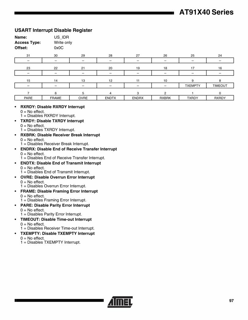
AT91X40 Series
USART Interrupt Disable RegisterName: US_IDRAccess Type: Write onlyOffset: 0x0C
• RXRDY: Disable RXRDY Interrupt0 = No effect.1 = Disables RXRDY Interrupt.
• TXRDY: Disable TXRDY Interrupt0 = No effect.1 = Disables TXRDY Interrupt.
• RXBRK: Disable Receiver Break Interrupt0 = No effect.1 = Disables Receiver Break Interrupt.
• ENDRX: Disable End of Receive Transfer Interrupt0 = No effect.1 = Disables End of Receive Transfer Interrupt.
• ENDTX: Disable End of Transmit Interrupt0 = No effect.1 = Disables End of Transmit Interrupt.
• OVRE: Disable Overrun Error Interrupt0 = No effect.1 = Disables Overrun Error Interrupt.
• FRAME: Disable Framing Error Interrupt0 = No effect.1 = Disables Framing Error Interrupt.
• PARE: Disable Parity Error Interrupt0 = No effect.1 = Disables Parity Error Interrupt.
• TIMEOUT: Disable Time-out Interrupt0 = No effect.1 = Disables Receiver Time-out Interrupt.
• TXEMPTY: Disable TXEMPTY Interrupt0 = No effect.1 = Disables TXEMPTY Interrupt.
31 30 29 28 27 26 25 24
– – – – – – – –
23 22 21 20 19 18 17 16
– – – – – – – –
15 14 13 12 11 10 9 8
– – – – – – TXEMPTY TIMEOUT
7 6 5 4 3 2 1 0
PARE FRAME OVRE ENDTX ENDRX RXBRK TXRDY RXRDY
97
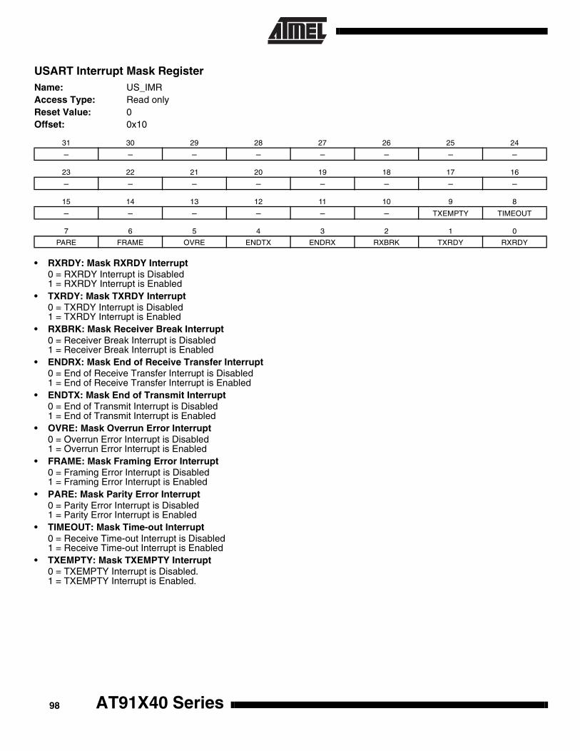
USART Interrupt Mask RegisterName: US_IMRAccess Type: Read onlyReset Value: 0Offset: 0x10
• RXRDY: Mask RXRDY Interrupt0 = RXRDY Interrupt is Disabled1 = RXRDY Interrupt is Enabled
• TXRDY: Mask TXRDY Interrupt0 = TXRDY Interrupt is Disabled1 = TXRDY Interrupt is Enabled
• RXBRK: Mask Receiver Break Interrupt0 = Receiver Break Interrupt is Disabled1 = Receiver Break Interrupt is Enabled
• ENDRX: Mask End of Receive Transfer Interrupt0 = End of Receive Transfer Interrupt is Disabled1 = End of Receive Transfer Interrupt is Enabled
• ENDTX: Mask End of Transmit Interrupt0 = End of Transmit Interrupt is Disabled1 = End of Transmit Interrupt is Enabled
• OVRE: Mask Overrun Error Interrupt0 = Overrun Error Interrupt is Disabled1 = Overrun Error Interrupt is Enabled
• FRAME: Mask Framing Error Interrupt0 = Framing Error Interrupt is Disabled1 = Framing Error Interrupt is Enabled
• PARE: Mask Parity Error Interrupt0 = Parity Error Interrupt is Disabled1 = Parity Error Interrupt is Enabled
• TIMEOUT: Mask Time-out Interrupt0 = Receive Time-out Interrupt is Disabled1 = Receive Time-out Interrupt is Enabled
• TXEMPTY: Mask TXEMPTY Interrupt0 = TXEMPTY Interrupt is Disabled.1 = TXEMPTY Interrupt is Enabled.
31 30 29 28 27 26 25 24
– – – – – – – –
23 22 21 20 19 18 17 16
– – – – – – – –
15 14 13 12 11 10 9 8
– – – – – – TXEMPTY TIMEOUT
7 6 5 4 3 2 1 0
PARE FRAME OVRE ENDTX ENDRX RXBRK TXRDY RXRDY
AT91X40 Series98

AT91X40 Series
USART Channel Status RegisterName: US_CSRAccess Type: Read onlyReset Value: 0x18Offset: 0x14
• RXRDY: Receiver Ready0 = No complete character has been received since the last read of the US_RHR or the receiver is disabled.1 = At least one complete character has been received and the US_RHR has not yet been read.
• TXRDY: Transmitter Ready0 = US_THR contains a character waiting to be transferred to the Transmit Shift Register, or an STTBRK command hasbeen requested.1 = US_THR is empty and there is no Break request pending TSR availability.Equal to zero when the USART is disabled or at reset. Transmitter Enable command (in US_CR) sets this bit to one.
• RXBRK: Break Received/End of Break0 = No Break Received nor End of Break has been detected since the last “Reset Status Bits” command in the ControlRegister.1 = Break Received or End of Break has been detected since the last “Reset Status Bits” command in the Control Reg-ister.
• ENDRX: End of Receiver Transfer0 = The End of Transfer signal from the Peripheral Data Controller channel dedicated to the receiver is inactive.1 = The End of Transfer signal from the Peripheral Data Controller channel dedicated to the receiver is active.
• ENDTX: End of Transmitter Transfer0 = The End of Transfer signal from the Peripheral Data Controller channel dedicated to the transmitter is inactive.1 = The End of Transfer signal from the Peripheral Data Controller channel dedicated to the transmitter is active.
• OVRE: Overrun Error0 = No byte has been transferred from the Receive Shift Register to the US_RHR when RxRDY was asserted since thelast “Reset Status Bits” command.1 = At least one byte has been transferred from the Receive Shift Register to the US_RHR when RxRDY was assertedsince the last “Reset Status Bits” command.
• FRAME: Framing Error0 = No stop bit has been detected low since the last “Reset Status Bits” command. 1 = At least one stop bit has been detected low since the last “Reset Status Bits” command.
• PARE: Parity Error1 = At least one parity bit has been detected false (or a parity bit high in Multi-drop Mode) since the last “Reset StatusBits” command.0 = No parity bit has been detected false (or a parity bit high in Multi-drop Mode) since the last “Reset Status Bits” com-mand.
• TIMEOUT: Receiver Time-out0 = There has not been a time-out since the last “Start Time-out” command or the Time-out Register is 0.1 = There has been a time-out since the last “Start Time-out” command.
• TXEMPTY: Transmitter Empty0 = There are characters in either US_THR or the Transmit Shift Register or a Break is being transmitted.1 = There are no characters in US_THR and the Transmit Shift Register and Break is not active.Equal to zero when the USART is disabled or at reset. Transmitter Enable command (in US_CR) sets this bit to one.
31 30 29 28 27 26 25 24
– – – – – – – –
23 22 21 20 19 18 17 16
– – – – – – – –
15 14 13 12 11 10 9 8
– – – – – – TXEMPTY TIMEOUT
7 6 5 4 3 2 1 0
PARE FRAME OVRE ENDTX ENDRX RXBRK TXRDY RXRDY
99
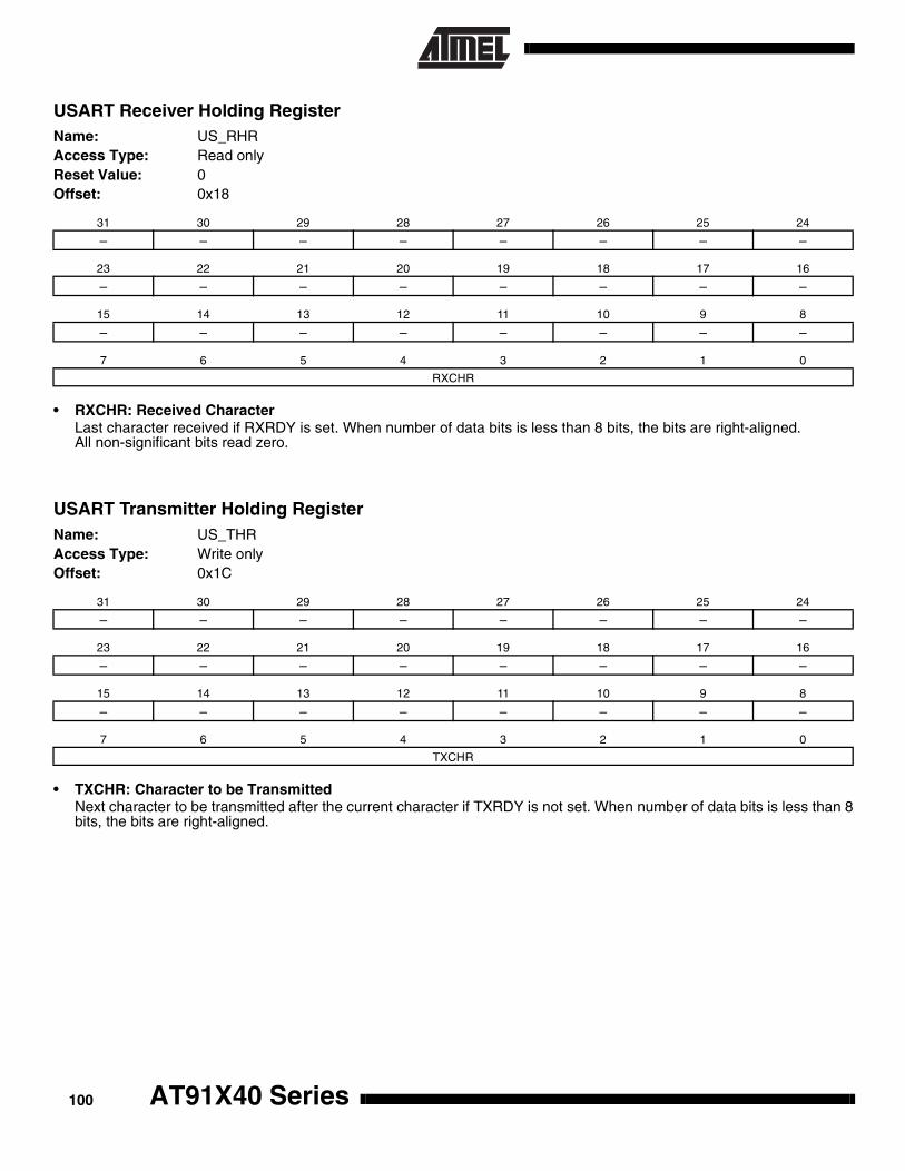
USART Receiver Holding RegisterName: US_RHRAccess Type: Read onlyReset Value: 0Offset: 0x18
• RXCHR: Received CharacterLast character received if RXRDY is set. When number of data bits is less than 8 bits, the bits are right-aligned.All non-significant bits read zero.
USART Transmitter Holding RegisterName: US_THRAccess Type: Write onlyOffset: 0x1C
• TXCHR: Character to be TransmittedNext character to be transmitted after the current character if TXRDY is not set. When number of data bits is less than 8bits, the bits are right-aligned.
31 30 29 28 27 26 25 24
– – – – – – – –
23 22 21 20 19 18 17 16
– – – – – – – –
15 14 13 12 11 10 9 8
– – – – – – – –
7 6 5 4 3 2 1 0
RXCHR
31 30 29 28 27 26 25 24
– – – – – – – –
23 22 21 20 19 18 17 16
– – – – – – – –
15 14 13 12 11 10 9 8
– – – – – – – –
7 6 5 4 3 2 1 0
TXCHR
AT91X40 Series100

AT91X40 Series
USART Baud Rate Generator RegisterName: US_BRGRAccess Type: Read/WriteReset Value: 0Offset: 0x20
• CD: Clock DivisorThis register has no effect if Synchronous Mode is selected with an external clock.
Notes: 1. Clock divisor bypass (CD = 1) must not be used when internal clock MCK is selected (USCLKS = 0).
2. In Synchronous Mode, the value programmed must be even to ensure a 50:50 mark:space ratio.
31 30 29 28 27 26 25 24
– – – – – – – –
23 22 21 20 19 18 17 16
– – – – – – – –
15 14 13 12 11 10 9 8
CD
7 6 5 4 3 2 1 0
CD
CD Effect
0 Disables Clock
1 Clock Divisor Bypass (1)
2 to 65535Baud Rate (Asynchronous Mode) = Selected Clock / (16 x CD) Baud Rate (Synchronous Mode) = Selected Clock / CD (2)
101

USART Receiver Time-out RegisterName: US_RTORAccess Type: Read/WriteReset Value: 0Offset: 0x24
• TO: Time-out ValueWhen a value is written to this register, a Start Time-out Command is automatically performed.
Time-out duration = TO x 4 x Bit period
USART Transmitter Time-guard RegisterName: US_TTGRAccess Type: Read/WriteReset Value: 0Offset: 0x28
• TG: Time-guard Value
Time-guard duration = TG x Bit period
31 30 29 28 27 26 25 24
– – – – – – – –
23 22 21 20 19 18 17 16
– – – – – – – –
15 14 13 12 11 10 9 8
– – – – – – – –
7 6 5 4 3 2 1 0
TO
TO
0 Disables the RX Time-out function.
1 - 255 The Time-out counter is loaded with TO when the Start Time-out Command is given or when each new data character is received (after reception has started).
31 30 29 28 27 26 25 24
– – – – – – – –
23 22 21 20 19 18 17 16
– – – – – – – –
15 14 13 12 11 10 9 8
– – – – – – – –
7 6 5 4 3 2 1 0
TG
TG
0 Disables the TX Time-guard function.
1 - 255 TXD is inactive high after the transmission of each character for the time-guard duration.
AT91X40 Series102
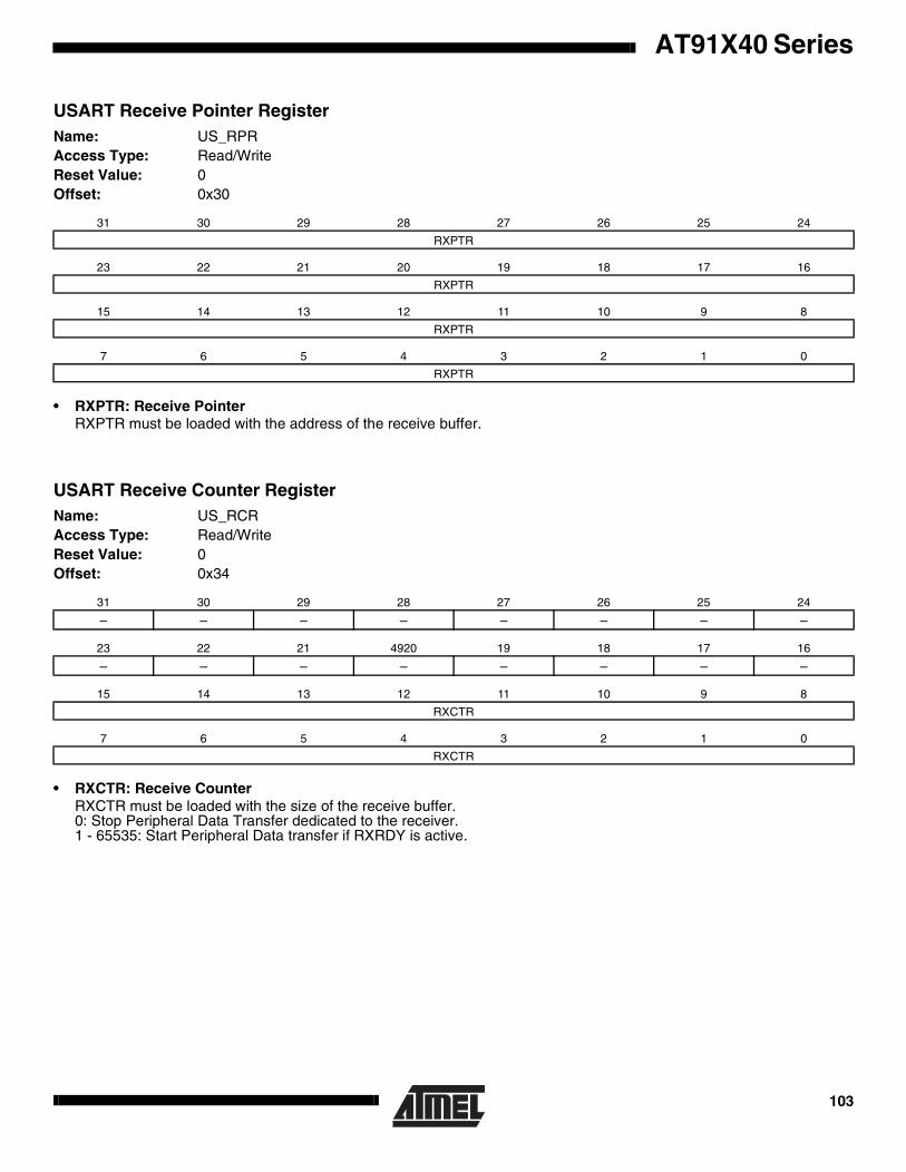
AT91X40 Series
USART Receive Pointer RegisterName: US_RPRAccess Type: Read/WriteReset Value: 0Offset: 0x30
• RXPTR: Receive PointerRXPTR must be loaded with the address of the receive buffer.
USART Receive Counter RegisterName: US_RCRAccess Type: Read/WriteReset Value: 0Offset: 0x34
• RXCTR: Receive CounterRXCTR must be loaded with the size of the receive buffer. 0: Stop Peripheral Data Transfer dedicated to the receiver.1 - 65535: Start Peripheral Data transfer if RXRDY is active.
31 30 29 28 27 26 25 24
RXPTR
23 22 21 20 19 18 17 16
RXPTR
15 14 13 12 11 10 9 8
RXPTR
7 6 5 4 3 2 1 0
RXPTR
31 30 29 28 27 26 25 24
– – – – – – – –
23 22 21 4920 19 18 17 16
– – – – – – – –
15 14 13 12 11 10 9 8
RXCTR
7 6 5 4 3 2 1 0
RXCTR
103

USART Transmit Pointer RegisterName: US_TPRAccess Type: Read/WriteReset Value: 0Offset: 0x38
• TXPTR: Transmit PointerTXPTR must be loaded with the address of the transmit buffer.
USART Transmit Counter RegisterName: US_TCRAccess Type: Read/WriteReset Value: 0Offset: 0x3C
• TXCTR: Transmit CounterTXCTR must be loaded with the size of the transmit buffer. 0: Stop Peripheral Data Transfer dedicated to the transmitter.1 - 65535: Start Peripheral Data transfer if TXRDY is active.
31 30 29 28 27 26 25 24
TXPTR
23 22 21 20 19 18 17 16
TXPTR
15 14 13 12 11 10 9 8
TXPTR
7 6 5 4 3 2 1 0
TXPTR
31 30 29 28 27 26 25 24
– – – – – – – –
23 22 21 20 19 18 17 16
– – – – – – – –
15 14 13 12 11 10 9 8
TXCTR
7 6 5 4 3 2 1 0
TXCTR
AT91X40 Series104

AT91X40 Series
TC: Timer Counter The AT91X40 Series features a Timer Counter block whichincludes three identical 16-bit timer counter channels. Eachchannel can be independently programmed to perform awide range of functions including frequency measurement,event counting, interval measurement, pulse generation,delay timing and pulse width modulation.
Each Timer Counter channel has 3 external clock inputs, 5internal clock inputs, and 2 multi-purpose input/output sig-nals which can be configured by the user. Each channel
drives an internal interrupt signal which can be pro-grammed to generate processor interrupts via the AIC(Advanced Interrupt Controller).
The Timer Counter block has two global registers which actupon all three TC channels. The Block Control Registerallows the three channels to be started simultaneously withthe same instruction. The Block Mode Register defines theexternal clock inputs for each Timer Counter channel,allowing them to be chained.
Figure 43. TC Block Diagram
Timer CounterChannel 0
Timer CounterChannel 1
Timer CounterChannel 2
SYNC
Parallel IOController
TC1XC1S
TC0XC0S
TC2XC2S
INT
INT
INT
TIOA0
TIOA1
TIOA2
TIOB0
TIOB1
TIOB2
XC0
XC1
XC2
XC0
XC1
XC2
XC0
XC1
XC2
TCLK0
TCLK1
TCLK2
TCLK0
TCLK1
TCLK2
TCLK0
TCLK1
TCLK2
TIOA1
TIOA2
TIOA0
TIOA2
TIOA0
TIOA1
AdvancedInterrupt
Controller
TCLK0TCLK1TCLK2
TIOA0TIOB0
TIOA1TIOB1
TIOA2TIOB2
Timer Counter Block
TIOA
TIOB
TIOA
TIOB
TIOA
TIOB
SYNC
SYNC
MCK/2
MCK/8
MCK/32
MCK/128
MCK/1024
105

Signal Name Description
Note: After a hardware reset, the Timer Counter block pins are controlled by the PIO Controller. They must be configured to be con-trolled by the peripheral before being used.
Timer Counter DescriptionThe three Timer Counter channels are independent andidentical in operation. The registers for channel program-ming are listed in Table 17.
Counter
Each Timer Counter channel is organized around a 16-bitcounter. The value of the counter is incremented at eachpositive edge of the selected clock. When the counter hasreached the value 0xFFFF and passes to 0x0000, an over-flow occurs and the bit COVFS in TC_SR (Status Register)is set.
The current value of the counter is accessible in real-timeby reading TC_CV. The counter can be reset by a trigger.In this case, the counter value passes to 0x0000 on thenext valid edge of the selected clock.
Clock Selection
At block level, input clock signals of each channel caneither be connected to the external inputs TCLK0, TCLK1or TCLK2, or be connected to the configurable I/O signalsTIOA0, TIOA1 or TIOA2 for chaining by programming theTC_BMR (Block Mode).
Each channel can independently select an internal or exter-nal clock source for its counter:• Internal clock signals: MCK/2, MCK/8, MCK/32,
MCK/128, MCK/1024
• External clock signals: XC0, XC1 or XC2
The selected clock can be inverted with the CLKI bit inTC_CMR (Channel Mode). This allows counting on theopposite edges of the clock.
The burst function allows the clock to be validated when anexternal signal is high. The BURST parameter in the ModeRegister defines this signal (none, XC0, XC1, XC2).
Note: In all cases, if an external clock is used, the duration of each of its levels must be longer than the system clock (MCK) period. The external clock frequency must be at least 2.5 times lower than the system clock (MCK).
Figure 44. Clock Selection
Channel Signal DescriptionXC0, XC1, XC2 External Clock Inputs
TIOACapture Mode: General Purpose InputWaveform Mode: General Purpose Input
TIOBCapture Mode: General Purpose InputWaveform Mode: General Purpose Input/Output
INT Interrupt Signal Output
SYNC Synchronization Input Signal
Block Signals DescriptionTCLK0, TCLK1, TCLK2 External Clock Inputs
TIOA0 TIOA Signal for Channel 0
TIOB0 TIOB Signal for Channel 0TIOA1 TIOA Signal for Channel 1TIOB1 TIOB Signal for Channel 1
TIOA2 TIOA Signal for Channel 2TIOB2 TIOB Signal for Channel 2
MCK/2
MCK/8
MCK/32
MCK/128
MCK/1024
XC0
XC1
XC2
CLKS
CLKI
BURST
1
SelectedClock
AT91X40 Series106
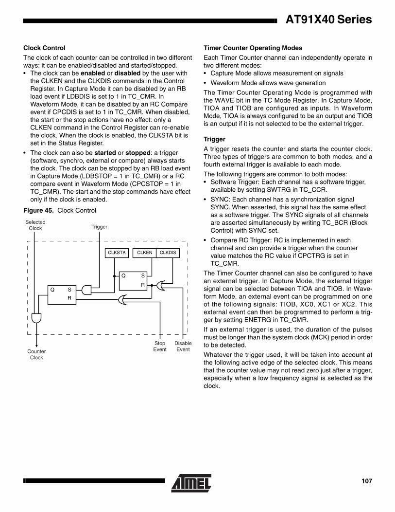
AT91X40 Series
Clock Control
The clock of each counter can be controlled in two differentways: it can be enabled/disabled and started/stopped.• The clock can be enabled or disabled by the user with
the CLKEN and the CLKDIS commands in the Control Register. In Capture Mode it can be disabled by an RB load event if LDBDIS is set to 1 in TC_CMR. In Waveform Mode, it can be disabled by an RC Compare event if CPCDIS is set to 1 in TC_CMR. When disabled, the start or the stop actions have no effect: only a CLKEN command in the Control Register can re-enable the clock. When the clock is enabled, the CLKSTA bit is set in the Status Register.
• The clock can also be started or stopped: a trigger (software, synchro, external or compare) always starts the clock. The clock can be stopped by an RB load event in Capture Mode (LDBSTOP = 1 in TC_CMR) or a RC compare event in Waveform Mode (CPCSTOP = 1 in TC_CMR). The start and the stop commands have effect only if the clock is enabled.
Figure 45. Clock Control
Timer Counter Operating Modes
Each Timer Counter channel can independently operate intwo different modes:• Capture Mode allows measurement on signals
• Waveform Mode allows wave generation
The Timer Counter Operating Mode is programmed withthe WAVE bit in the TC Mode Register. In Capture Mode,TIOA and TIOB are configured as inputs. In WaveformMode, TIOA is always configured to be an output and TIOBis an output if it is not selected to be the external trigger.
Trigger
A trigger resets the counter and starts the counter clock.Three types of triggers are common to both modes, and afourth external trigger is available to each mode.
The following triggers are common to both modes:• Software Trigger: Each channel has a software trigger,
available by setting SWTRG in TC_CCR.
• SYNC: Each channel has a synchronization signal SYNC. When asserted, this signal has the same effect as a software trigger. The SYNC signals of all channels are asserted simultaneously by writing TC_BCR (Block Control) with SYNC set.
• Compare RC Trigger: RC is implemented in each channel and can provide a trigger when the counter value matches the RC value if CPCTRG is set in TC_CMR.
The Timer Counter channel can also be configured to havean external trigger. In Capture Mode, the external triggersignal can be selected between TIOA and TIOB. In Wave-form Mode, an external event can be programmed on oneof the following signals: TIOB, XC0, XC1 or XC2. Thisexternal event can then be programmed to perform a trig-ger by setting ENETRG in TC_CMR.
If an external trigger is used, the duration of the pulsesmust be longer than the system clock (MCK) period in orderto be detected.
Whatever the trigger used, it will be taken into account atthe following active edge of the selected clock. This meansthat the counter value may not read zero just after a trigger,especially when a low frequency signal is selected as theclock.
Q S
R
S
R
Q
CLKSTA CLKEN CLKDIS
StopEvent
DisableEventCounter
Clock
SelectedClock Trigger
107

Capture Operating Mode This mode is entered by clearing the WAVE parameter inTC_CMR (Channel Mode Register). Capture Mode allowsthe TC Channel to perform measurements such as pulsetiming, frequency, period, duty cycle and phase on TIOAand TIOB signals which are inputs.
Figure 46 shows the configuration of the TC Channel whenprogrammed in Capture Mode.
Capture Registers A and B (RA and RB)
Registers A and B are used as capture registers. Thismeans that they can be loaded with the counter value whena programmable event occurs on the signal TIOA.
The parameter LDRA in TC_CMR defines the TIOA edgefor the loading of register A, and the parameter LDRBdefines the TIOA edge for the loading of Register B.
RA is loaded only if it has not been loaded since the lasttrigger or if RB has been loaded since the last loading ofRA.
RB is loaded only if RA has been loaded since the last trig-ger or the last loading of RB.
Loading RA or RB before the read of the last value loadedsets the Overrun Error Flag (LOVRS) in TC_SR (StatusRegister). In this case, the old value is overwritten.
Trigger Conditions
In addition to the SYNC signal, the software trigger and theRC compare trigger, an external trigger can be defined.
Bit ABETRG in TC_CMR selects input signal TIOA or TIOBas an external trigger. Parameter ETRGEDG defines theedge (rising, falling or both) detected to generate an exter-nal trigger. If ETRGEDG = 0 (none), the external trigger isdisabled.
Status Register
The following bits in the status register are significant inCapture Operating Mode. • CPCS: RC Compare Status
There has been an RC Compare match at least oncesince the last read of the status
• COVFS: Counter Overflow Status
The counter has attempted to count past $FFFF sincethe last read of the status
• LOVRS: Load Overrun Status
RA or RB has been loaded at least twice without anyread of the corresponding register, since the last readof the status
• LDRAS: Load RA Status
RA has been loaded at least once without any read,since the last read of the status
• LDRBS: Load RB Status
RB has been loaded at least once without any read,since the last read of the status
• ETRGS: External Trigger Status
An external trigger on TIOA or TIOB has been detectedsince the last read of the status
AT91X40 Series108

AT91X40 Series
Figure 46. Capture Mode
MC
K/2
MC
K/8
MC
K/3
2
MC
K/1
28
MC
K/1
024
XC
0
XC
1
XC
2
TCC
LKS
CLK
I
QS R
S R
Q
CLK
STA
CLK
EN
CLK
DIS
BU
RS
T
TIO
B
Reg
iste
r C
Cap
ture
R
egis
ter A
C
aptu
re
Reg
iste
r BC
ompa
re R
C =
16-b
it C
ount
er
AB
ETR
G
SW
TRG
ETR
GE
DG
CP
CTR
G
TC_IMR
Trig
LDRBS
LDRAS
ETRGS
TC_SR
LOVRS
COVFS
SY
NC
1
MTI
OB
TIO
A
MTI
OA
LDR
A
LDB
STO
P
If R
A is
not
load
edor
RB
is lo
aded
If R
A is
load
ed
LDB
DIS
CPCS
INT
Edg
e D
etec
tor
Edg
e D
etec
tor
LDR
B
Edg
e D
etec
tor
CLK
OV
F
RE
SE
T
Tim
er C
ount
er C
hann
el
109

Waveform Operating ModeThis mode is entered by setting the WAVE parameter inTC_CMR (Channel Mode Register).
Waveform Operating Mode allows the TC Channel to gen-erate 1 or 2 PWM signals with the same frequency andindependently programmable duty cycles, or to generatedifferent types of one-shot or repetitive pulses.
In this mode, TIOA is configured as output and TIOB isdefined as output if it is not used as an external event(EEVT parameter in TC_CMR).
Figure 47 shows the configuration of the TC Channel whenprogrammed in Waveform Operating Mode.
Compare Register A, B and C (RA, RB, and RC)
In Waveform Operating Mode, RA, RB and RC are all usedas compare registers.
RA Compare is used to control the TIOA output. RB Com-pare is used to control the TIOB (if configured as output).RC Compare can be programmed to control TIOA and/orTIOB outputs.
RC Compare can also stop the counter clock (CPCSTOP =1 in TC_CMR) and/or disable the counter clock (CPCDIS =1 in TC_CMR).
As in Capture Mode, RC Compare can also generate a trig-ger if CPCTRG = 1. A trigger resets the counter so RC cancontrol the period of PWM waveforms.
External Event/Trigger Conditions
An external event can be programmed to be detected onone of the clock sources (XC0, XC1, XC2) or TIOB. Theexternal event selected can then be used as a trigger.
The parameter EEVT in TC_CMR selects the external trig-ger. The parameter EEVTEDG defines the trigger edge foreach of the possible external triggers (rising, falling orboth). If EEVTEDG is cleared (none), no external event isdefined.
If TIOB is defined as an external event signal (EEVT = 0),TIOB is no longer used as output and the TC channel canonly generate a waveform on TIOA.
When an external event is defined, it can be used as a trig-ger by setting bit ENETRG in TC_CMR.
As in Capture Mode, the SYNC signal, the software triggerand the RC compare trigger are also available as triggers.
Output Controller
The output controller defines the output level changes onTIOA and TIOB following an event. TIOB control is usedonly if TIOB is defined as output (not as an external event).
The following events control TIOA and TIOB: software trig-ger, external event and RC compare. RA compare controlsTIOA and RB compare controls TIOB. Each of these
events can be programmed to set, clear or toggle the out-put as defined in the corresponding parameter in TC_CMR.
The tables below show which parameter in TC_CMR isused to define the effect of each event.
If two or more events occur at the same time, the prioritylevel is defined as follows:
1. Software Trigger
2. External Event
3. RC Compare
4. RA or RB Compare
Status
The following bits in the status register are significant inWaveform Mode:• CPAS: RA Compare Status
There has been a RA Compare match at least oncesince the last read of the status
• CPBS: RB Compare Status
There has been a RB Compare match at least oncesince the last read of the status
• CPCS: RC Compare Status
There has been a RC Compare match at least oncesince the last read of the status
• COVFS: Counter Overflow
Counter has attempted to count past $FFFF since thelast read of the status
• ETRGS: External Trigger
External trigger has been detected since the last readof the status
Parameter TIOA Event
ASWTRG Software Trigger
AEEVT External Event
ACPC RC Compare
ACPA RA Compare
Parameter TIOB Event
BSWTRG Software Trigger
BEEVT External Event
BCPC RC Compare
BCPB RB Compare
AT91X40 Series110
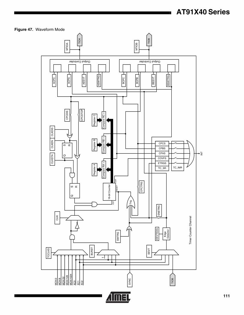
AT91X40 Series
Figure 47. Waveform Mode
MC
K/2
MC
K/8
MC
K/3
2
MC
K/1
28
MC
K/1
024
XC
0
XC
1
XC
2
TC
CLK
S
CLK
I
QS R
S R
Q
CLK
ST
AC
LKE
NC
LKD
IS
CP
CD
IS
BU
RS
T
TIO
B
Reg
iste
r A
Reg
iste
r B
Reg
iste
r C
Com
pare
RA
=
Com
pare
RB
=
Com
pare
RC
=
CP
CS
TO
P
16-b
it C
ount
er
EE
VT
EE
VT
ED
G
SY
NC
SW
TR
G
EN
ET
RG
CP
CT
RG
TC_IMR
Trig
AC
PC
AC
PA
AE
EV
T
AS
WT
RG
BC
PC
BC
PB
BE
EV
T
BS
WT
RG
TIO
A
MT
IOA T
IOB
MT
IOB
CPAS
COVFS
ETRGS
TC_SR
CPCS
CPBS
CLK
OV
FR
ES
ET
Output Controller Output Controller
INT
1
Edg
e D
etec
tor
Tim
er C
ount
er C
hann
el
111

TC User InterfaceTC Base Address: 0xFFFE0000
TC_BCR (Block Control Register) and TC_BMR (Block Mode Register) control the TC block. TC Channels are controlledby the registers listed in Table 17. The offset of each of the Channel registers in Table 17 is in relation to the offset of thecorresponding channel as mentioned in Table 16.
Note: Read only if WAVE = 0
Table 16. TC Global Memory Map
Offset Channel/Register Name Access Reset State
0x00 TC Channel 0 See Table 17
0x40 TC Channel 1 See Table 17
0x80 TC Channel 2 See Table 17
0xC0 TC Block Control Register TC_BCR Write Only –
0xC4 TC Block Mode Register TC_BMR Read/Write 0
Table 17. TC Channel Memory Map
Offset Register Name Access Reset State
0x00 Channel Control Register TC_CCR Write Only –
0x04 Channel Mode Register TC_CMR Read/Write 0
0x08 Reserved –
0x0C Reserved –
0x10 Counter Value TC_CV Read/Write 0
0x14 Register A TC_RA Read/Write(1) 0
0x18 Register B TC_RB Read/Write(1) 0
0x1C Register C TC_RC Read/Write 0
0x20 Status Register TC_SR Read Only 0
0x24 Interrupt Enable Register TC_IER Write Only –
0x28 Interrupt Disable Register TC_IDR Write Only –
0x2C Interrupt Mask Register TC_IMR Read Only 0
AT91X40 Series112

AT91X40 Series
TC Block Control Register Register Name: TC_BCRAccess Type: Write onlyOffset: 0xC0
• SYNC: Synchro Command0 = No effect.1 = Asserts the SYNC signal which generates a software trigger simultaneously for each of the channels.
31 30 29 28 27 26 25 24
– – – – – – – –
23 22 21 20 19 18 17 16
– – – – – – – –
15 14 13 12 11 10 9 8
– – – – – – – –
7 6 5 4 3 2 1 0
– – – – – – – SYNC
113
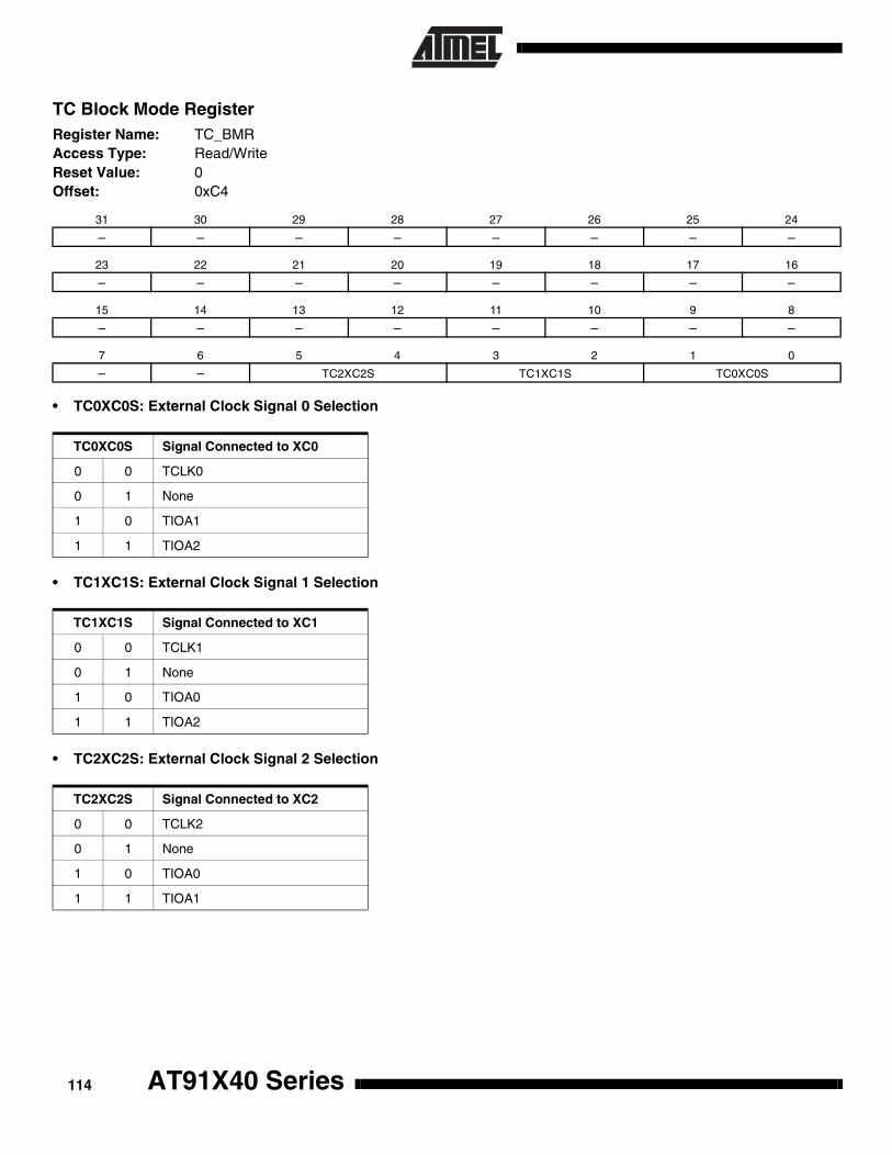
TC Block Mode Register Register Name: TC_BMRAccess Type: Read/WriteReset Value: 0Offset: 0xC4
• TC0XC0S: External Clock Signal 0 Selection
• TC1XC1S: External Clock Signal 1 Selection
• TC2XC2S: External Clock Signal 2 Selection
31 30 29 28 27 26 25 24
– – – – – – – –
23 22 21 20 19 18 17 16
– – – – – – – –
15 14 13 12 11 10 9 8
– – – – – – – –
7 6 5 4 3 2 1 0
– – TC2XC2S TC1XC1S TC0XC0S
TC0XC0S Signal Connected to XC0
0 0 TCLK0
0 1 None
1 0 TIOA1
1 1 TIOA2
TC1XC1S Signal Connected to XC1
0 0 TCLK1
0 1 None
1 0 TIOA0
1 1 TIOA2
TC2XC2S Signal Connected to XC2
0 0 TCLK2
0 1 None
1 0 TIOA0
1 1 TIOA1
AT91X40 Series114
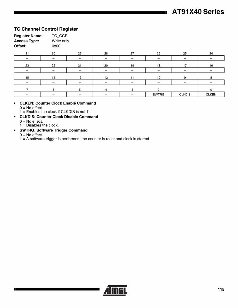
AT91X40 Series
TC Channel Control Register Register Name: TC_CCRAccess Type: Write onlyOffset: 0x00
• CLKEN: Counter Clock Enable Command0 = No effect.1 = Enables the clock if CLKDIS is not 1.
• CLKDIS: Counter Clock Disable Command0 = No effect.1 = Disables the clock.
• SWTRG: Software Trigger Command0 = No effect.1 = A software trigger is performed: the counter is reset and clock is started.
31 30 29 28 27 26 25 24
– – – – – – – –
23 22 21 20 19 18 17 16
– – – – – – – –
15 14 13 12 11 10 9 8
– – – – – – – –
7 6 5 4 3 2 1 0
– – – – – SWTRG CLKDIS CLKEN
115

TC Channel Mode Register: Capture ModeRegister Name: TC_CMRAccess Type: Read/WriteReset Value: 0Offset: 0x04
• TCCLKS: Clock Selection
• CLKI: Clock Invert 0 = Counter is incremented on rising edge of the clock.1 = Counter is incremented on falling edge of the clock.
• BURST: Burst Signal Selection
• LDBSTOP: Counter Clock Stopped with RB Loading0 = Counter clock is not stopped when RB loading occurs.1 = Counter clock is stopped when RB loading occurs.
• LDBDIS: Counter Clock Disable with RB Loading 0 = Counter clock is not disabled when RB loading occurs.1 = Counter clock is disabled when RB loading occurs.
31 30 29 28 27 26 25 24
– – – – – – – –
23 22 21 20 19 18 17 16
– – – – LDRB LDRA
15 14 13 12 11 10 9 8
WAVE = 0 CPCTRG – – – ABETRG ETRGEDG
7 6 5 4 3 2 1 0
LDBDIS LDBSTOP BURST CLKI TCCLKS
TCCLKS Clock Selected
0 0 0 MCK/2
0 0 1 MCK/8
0 1 0 MCK/32
0 1 1 MCK/128
1 0 0 MCK/1024
1 0 1 XC0
1 1 0 XC1
1 1 1 XC2
BURST
0 0 The clock is not gated by an external signal
0 1 XC0 is ANDed with the selected clock
1 0 XC1 is ANDed with the selected clock
1 1 XC2 is ANDed with the selected clock
AT91X40 Series116

AT91X40 Series
• ETRGEDG: External Trigger Edge Selection
• ABETRG: TIOA or TIOB External Trigger Selection0 = TIOB is used as an external trigger.1 = TIOA is used as an external trigger.
• CPCTRG: RC Compare Trigger Enable0 = RC Compare has no effect on the counter and its clock.1 = RC Compare resets the counter and starts the counter clock.
• WAVE = 0 0 = Capture Mode is enabled.1 = Capture Mode is disabled (Waveform Mode is enabled).
• LDRA: RA Loading Selection
• LDRB: RB Loading Selection
ETRGEDG Edge
0 0 None
0 1 Rising Edge
1 0 Falling Edge
1 1 Each Edge
LDRA Edge
0 0 None
0 1 Rising Edge of TIOA
1 0 Falling Edge of TIOA
1 1 Each Edge of TIOA
LDRB Edge
0 0 None
0 1 Rising Edge of TIOA
1 0 Falling Edge of TIOA
1 1 Each Edge of TIOA
117

TC Channel Mode Register: Waveform ModeRegister Name: TC_CMRAccess Type: Read/WriteReset Value: 0Offset: 0x04
• TCCLKS: Clock Selection
• CLKI: Clock Invert 0 = Counter is incremented on rising edge of the clock.1 = Counter is incremented on falling edge of the clock.
• BURST: Burst Signal Selection
• CPCSTOP: Counter Clock Stopped with RC Compare0 = Counter clock is not stopped when counter reaches RC.1 = Counter clock is stopped when counter reaches RC.
• CPCDIS: Counter Clock Disable with RC Compare0 = Counter clock is not disabled when counter reaches RC.1 = Counter clock is disabled when counter reaches RC.
31 30 29 28 27 26 25 24
BSWTRG BEEVT BCPC BCPB
23 22 21 20 19 18 17 16
ASWTRG AEEVT ACPC ACPA
15 14 13 12 11 10 9 8
WAVE = 1 CPCTRG – ENETRG EEVT EEVTEDG
7 6 5 4 3 2 1 0
CPCDIS CPCSTOP BURST CLKI TCCLKS
TCCLKS Clock Selected
0 0 0 MCK/2
0 0 1 MCK/8
0 1 0 MCK/32
0 1 1 MCK/128
1 0 0 MCK/1024
1 0 1 XC0
1 1 0 XC1
1 1 1 XC2
BURST
0 0 The clock is not gated by an external signal.
0 1 XC0 is ANDed with the selected clock.
1 0 XC1 is ANDed with the selected clock.
1 1 XC2 is ANDed with the selected clock.
AT91X40 Series118

AT91X40 Series
• EEVTEDG: External Event Edge Selection
• EEVT: External Event Selection
Note: If TIOB is chosen as the external event signal, it is configured as an input and no longer generates waveforms.
• ENETRG: External Event Trigger Enable0 = The external event has no effect on the counter and its clock. In this case, the selected external event only controlsthe TIOA output.1 = The external event resets the counter and starts the counter clock.
• CPCTRG: RC Compare Trigger Enable0 = RC Compare has no effect on the counter and its clock.1 = RC Compare resets the counter and starts the counter clock.
• WAVE = 1 0 = Waveform Mode is disabled (Capture Mode is enabled).1 = Waveform Mode is enabled.
• ACPA: RA Compare Effect on TIOA
• ACPC: RC Compare Effect on TIOA
EEVTEDG Edge
0 0 None
0 1 Rising Edge
1 0 Falling Edge
1 1 Each Edge
EEVT
Signal Selected as External Event TIOB Direction
0 0 TIOB Input(1)
0 1 XC0 Output
1 0 XC1 Output
1 1 XC2 Output
ACPA Effect
0 0 None
0 1 Set
1 0 Clear
1 1 Toggle
ACPC Effect
0 0 None
0 1 Set
1 0 Clear
1 1 Toggle
119

• AEEVT: External Event Effect on TIOA
• ASWTRG: Software Trigger Effect on TIOA
• BCPB: RB Compare Effect on TIOB
• BCPC: RC Compare Effect on TIOB
• BEEVT: External Event Effect on TIOB
• BSWTRG: Software Trigger Effect on TIOB
AEEVT Effect
0 0 None
0 1 Set
1 0 Clear
1 1 Toggle
ASWTRG Effect
0 0 None
0 1 Set
1 0 Clear
1 1 Toggle
BCPB Effect
0 0 None
0 1 Set
1 0 Clear
1 1 Toggle
BCPC Effect
0 0 None
0 1 Set
1 0 Clear
1 1 Toggle
BEEVT Effect
0 0 None
0 1 Set
1 0 Clear
1 1 Toggle
BSWTRG Effect
0 0 None
0 1 Set
1 0 Clear
1 1 Toggle
AT91X40 Series120
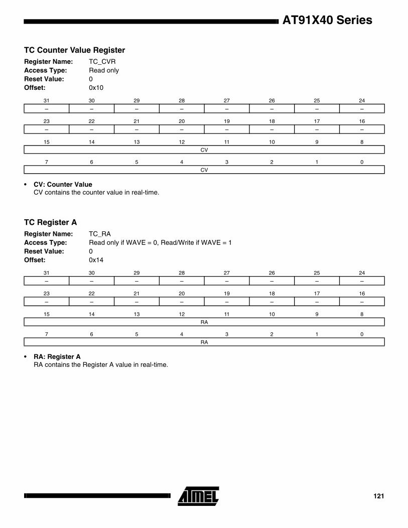
AT91X40 Series
TC Counter Value Register Register Name: TC_CVRAccess Type: Read onlyReset Value: 0Offset: 0x10
• CV: Counter ValueCV contains the counter value in real-time.
TC Register ARegister Name: TC_RAAccess Type: Read only if WAVE = 0, Read/Write if WAVE = 1Reset Value: 0Offset: 0x14
• RA: Register ARA contains the Register A value in real-time.
31 30 29 28 27 26 25 24
– – – – – – – –
23 22 21 20 19 18 17 16
– – – – – – – –
15 14 13 12 11 10 9 8
CV
7 6 5 4 3 2 1 0
CV
31 30 29 28 27 26 25 24
– – – – – – – –
23 22 21 20 19 18 17 16
– – – – – – – –
15 14 13 12 11 10 9 8
RA
7 6 5 4 3 2 1 0
RA
121
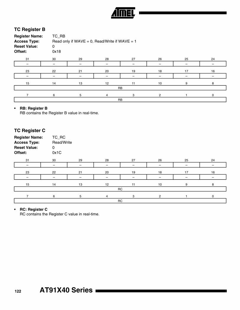
TC Register BRegister Name: TC_RBAccess Type: Read only if WAVE = 0, Read/Write if WAVE = 1Reset Value: 0Offset: 0x18
• RB: Register BRB contains the Register B value in real-time.
TC Register CRegister Name: TC_RCAccess Type: Read/WriteReset Value: 0Offset: 0x1C
• RC: Register CRC contains the Register C value in real-time.
31 30 29 28 27 26 25 24
– – – – – – – –
23 22 21 20 19 18 17 16
– – – – – – – –
15 14 13 12 11 10 9 8
RB
7 6 5 4 3 2 1 0
RB
31 30 29 28 27 26 25 24
– – – – – – – –
23 22 21 20 19 18 17 16
– – – – – – – –
15 14 13 12 11 10 9 8
RC
7 6 5 4 3 2 1 0
RC
AT91X40 Series122
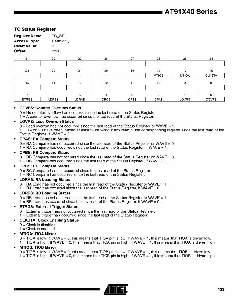
AT91X40 Series
TC Status Register Register Name: TC_SRAccess Type: Read onlyReset Value: 0Offset: 0x20
• COVFS: Counter Overflow Status0 = No counter overflow has occurred since the last read of the Status Register.1 = A counter overflow has occurred since the last read of the Status Register.
• LOVRS: Load Overrun Status0 = Load overrun has not occurred since the last read of the Status Register or WAVE = 1.1 = RA or RB have been loaded at least twice without any read of the corresponding register since the last read of theStatus Register, if WAVE = 0.
• CPAS: RA Compare Status0 = RA Compare has not occurred since the last read of the Status Register or WAVE = 0.1 = RA Compare has occurred since the last read of the Status Register, if WAVE = 1.
• CPBS: RB Compare Status0 = RB Compare has not occurred since the last read of the Status Register or WAVE = 0.1 = RB Compare has occurred since the last read of the Status Register, if WAVE = 1.
• CPCS: RC Compare Status0 = RC Compare has not occurred since the last read of the Status Register.1 = RC Compare has occurred since the last read of the Status Register.
• LDRAS: RA Loading Status0 = RA Load has not occurred since the last read of the Status Register or WAVE = 1.1 = RA Load has occurred since the last read of the Status Register, if WAVE = 0.
• LDRBS: RB Loading Status0 = RB Load has not occurred since the last read of the Status Register or WAVE = 1.1 = RB Load has occurred since the last read of the Status Register, if WAVE = 0.
• ETRGS: External Trigger Status0 = External trigger has not occurred since the last read of the Status Register.1 = External trigger has occurred since the last read of the Status Register.
• CLKSTA: Clock Enabling Status0 = Clock is disabled.1 = Clock is enabled.
• MTIOA: TIOA Mirror0 = TIOA is low. If WAVE = 0, this means that TIOA pin is low. If WAVE = 1, this means that TIOA is driven low.1 = TIOA is high. If WAVE = 0, this means that TIOA pin is high. If WAVE = 1, this means that TIOA is driven high.
• MTIOB: TIOB Mirror 0 = TIOB is low. If WAVE = 0, this means that TIOB pin is low. If WAVE = 1, this means that TIOB is driven low.1 = TIOB is high. If WAVE = 0, this means that TIOB pin is high. If WAVE = 1, this means that TIOB is driven high.
31 30 29 28 27 26 25 24
– – – – – – – –
23 22 21 20 19 18 17 16
– – – – – MTIOB MTIOA CLKSTA
15 14 13 12 11 10 9 8
– – – – – – – –
7 6 5 4 3 2 1 0
ETRGS LDRBS LDRAS CPCS CPBS CPAS LOVRS COVFS
123
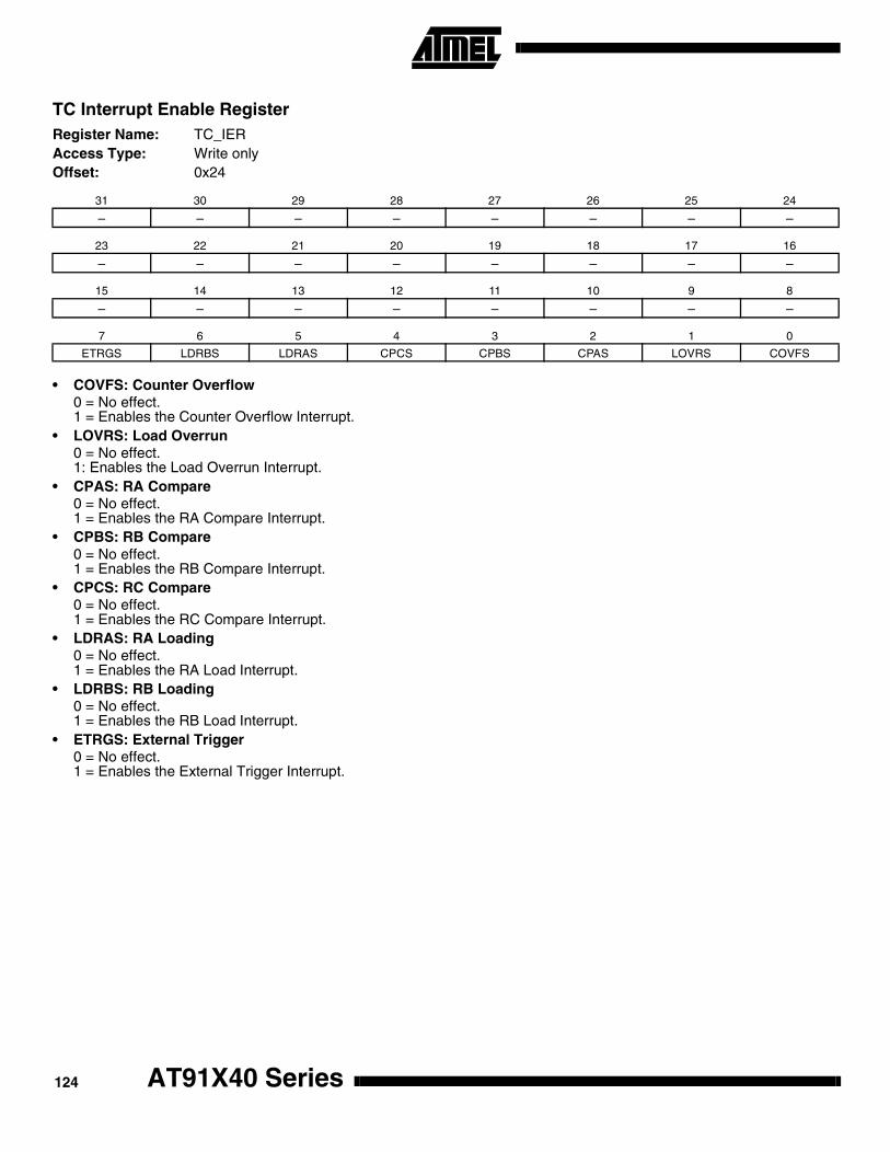
TC Interrupt Enable Register Register Name: TC_IERAccess Type: Write onlyOffset: 0x24
• COVFS: Counter Overflow 0 = No effect.1 = Enables the Counter Overflow Interrupt.
• LOVRS: Load Overrun 0 = No effect.1: Enables the Load Overrun Interrupt.
• CPAS: RA Compare 0 = No effect.1 = Enables the RA Compare Interrupt.
• CPBS: RB Compare 0 = No effect.1 = Enables the RB Compare Interrupt.
• CPCS: RC Compare 0 = No effect.1 = Enables the RC Compare Interrupt.
• LDRAS: RA Loading 0 = No effect.1 = Enables the RA Load Interrupt.
• LDRBS: RB Loading 0 = No effect.1 = Enables the RB Load Interrupt.
• ETRGS: External Trigger 0 = No effect.1 = Enables the External Trigger Interrupt.
31 30 29 28 27 26 25 24
– – – – – – – –
23 22 21 20 19 18 17 16
– – – – – – – –
15 14 13 12 11 10 9 8
– – – – – – – –
7 6 5 4 3 2 1 0
ETRGS LDRBS LDRAS CPCS CPBS CPAS LOVRS COVFS
AT91X40 Series124
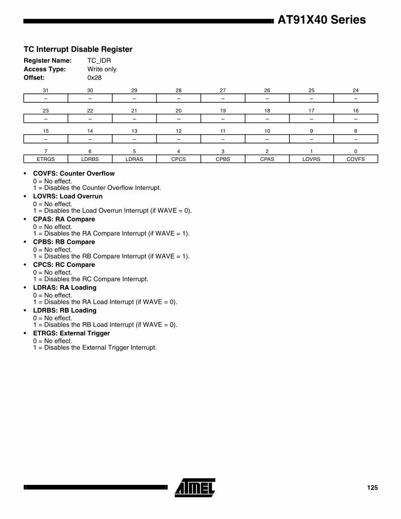
AT91X40 Series
TC Interrupt Disable Register Register Name: TC_IDRAccess Type: Write only Offset: 0x28
• COVFS: Counter Overflow 0 = No effect.1 = Disables the Counter Overflow Interrupt.
• LOVRS: Load Overrun 0 = No effect.1 = Disables the Load Overrun Interrupt (if WAVE = 0).
• CPAS: RA Compare 0 = No effect.1 = Disables the RA Compare Interrupt (if WAVE = 1).
• CPBS: RB Compare 0 = No effect.1 = Disables the RB Compare Interrupt (if WAVE = 1).
• CPCS: RC Compare 0 = No effect.1 = Disables the RC Compare Interrupt.
• LDRAS: RA Loading 0 = No effect.1 = Disables the RA Load Interrupt (if WAVE = 0).
• LDRBS: RB Loading 0 = No effect.1 = Disables the RB Load Interrupt (if WAVE = 0).
• ETRGS: External Trigger 0 = No effect.1 = Disables the External Trigger Interrupt.
31 30 29 28 27 26 25 24
– – – – – – – –
23 22 21 20 19 18 17 16
– – – – – – – –
15 14 13 12 11 10 9 8
– – – – – – – –
7 6 5 4 3 2 1 0
ETRGS LDRBS LDRAS CPCS CPBS CPAS LOVRS COVFS
125
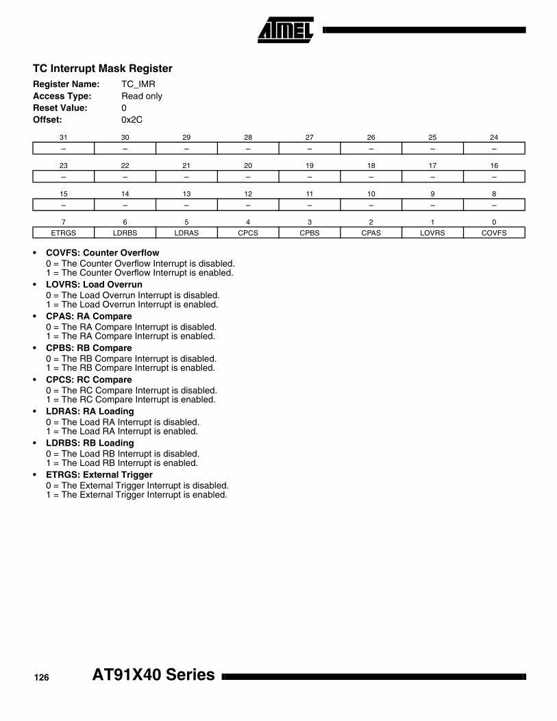
TC Interrupt Mask Register Register Name: TC_IMRAccess Type: Read onlyReset Value: 0Offset: 0x2C
• COVFS: Counter Overflow 0 = The Counter Overflow Interrupt is disabled.1 = The Counter Overflow Interrupt is enabled.
• LOVRS: Load Overrun 0 = The Load Overrun Interrupt is disabled.1 = The Load Overrun Interrupt is enabled.
• CPAS: RA Compare 0 = The RA Compare Interrupt is disabled.1 = The RA Compare Interrupt is enabled.
• CPBS: RB Compare 0 = The RB Compare Interrupt is disabled.1 = The RB Compare Interrupt is enabled.
• CPCS: RC Compare 0 = The RC Compare Interrupt is disabled.1 = The RC Compare Interrupt is enabled.
• LDRAS: RA Loading 0 = The Load RA Interrupt is disabled.1 = The Load RA Interrupt is enabled.
• LDRBS: RB Loading 0 = The Load RB Interrupt is disabled.1 = The Load RB Interrupt is enabled.
• ETRGS: External Trigger 0 = The External Trigger Interrupt is disabled.1 = The External Trigger Interrupt is enabled.
31 30 29 28 27 26 25 24
– – – – – – – –
23 22 21 20 19 18 17 16
– – – – – – – –
15 14 13 12 11 10 9 8
– – – – – – – –
7 6 5 4 3 2 1 0
ETRGS LDRBS LDRAS CPCS CPBS CPAS LOVRS COVFS
AT91X40 Series126

© Atmel Corporation 2000.Atmel Corporation makes no warranty for the use of its products, other than those expressly contained in the Company’s standard war-ranty which is detailed in Atmel’s Terms and Conditions located on the Company’s web site. The Company assumes no responsibility forany errors which may appear in this document, reserves the right to change devices or specifications detailed herein at any time withoutnotice, and does not make any commitment to update the information contained herein. No licenses to patents or other intellectual prop-erty of Atmel are granted by the Company in connection with the sale of Atmel products, expressly or by implication. Atmel’s products arenot authorized for use as critical components in life support devices or systems.
Atmel Headquarters Atmel Operations
Corporate Headquarters2325 Orchard ParkwaySan Jose, CA 95131TEL (408) 441-0311FAX (408) 487-2600
EuropeAtmel U.K., Ltd.Coliseum Business CentreRiverside WayCamberley, Surrey GU15 3YLEnglandTEL (44) 1276-686-677FAX (44) 1276-686-697
AsiaAtmel Asia, Ltd.Room 1219Chinachem Golden Plaza77 Mody Road TsimhatsuiEast KowloonHong KongTEL (852) 2721-9778FAX (852) 2722-1369
JapanAtmel Japan K.K.9F, Tonetsu Shinkawa Bldg.1-24-8 ShinkawaChuo-ku, Tokyo 104-0033JapanTEL (81) 3-3523-3551FAX (81) 3-3523-7581
Atmel Colorado Springs1150 E. Cheyenne Mtn. Blvd.Colorado Springs, CO 80906TEL (719) 576-3300FAX (719) 540-1759
Atmel RoussetZone Industrielle13106 Rousset CedexFranceTEL (33) 4-4253-6000FAX (33) 4-4253-6001
Fax-on-DemandNorth America:1-(800) 292-8635
International:1-(408) 441-0732
Web Sitehttp://www.atmel.com
BBS1-(408) 436-4309
Printed on recycled paper.
1354B-07/00/0M
Marks bearing ® and/or ™ are registered trademarks and trademarks of Atmel Corporation.Terms and product names in this document may be trademarks of others.ARM, Thumb and ARM Powered are registered trademarks of ARM Limited. ARM7TDMI is a trademark of ARM Ltd.