artisan technology group is your source for quality … · 2013-11-12 · artisan technology group...
TRANSCRIPT

Artisan Technology Group is your source for quality new and certified-used/pre-owned equipment
• FAST SHIPPING AND DELIVERY
• TENS OF THOUSANDS OF IN-STOCK ITEMS
• EQUIPMENT DEMOS
• HUNDREDS OF MANUFACTURERS SUPPORTED
• LEASING/MONTHLY RENTALS
• ITAR CERTIFIED SECURE ASSET SOLUTIONS
SERVICE CENTER REPAIRSExperienced engineers and technicians on staff at our full-service, in-house repair center
WE BUY USED EQUIPMENTSell your excess, underutilized, and idle used equipment We also offer credit for buy-backs and trade-inswww.artisantg.com/WeBuyEquipment
REMOTE INSPECTIONRemotely inspect equipment before purchasing with our interactive website at www.instraview.com
LOOKING FOR MORE INFORMATION? Visit us on the web at www.artisantg.com for more information on price quotations, drivers, technical specifications, manuals, and documentation
Contact us: (888) 88-SOURCE | [email protected] | www.artisantg.com
SMViewInstra
PENTLAND SYSTEMS LIMITED
OPERATING MANUAL
MPV905
Pentland Systems Limited 1 Cochrane Square Brucefield Industrial Park LIVINGSTON West Lothian Scotland EH54 9DR
Telephone: (0506) 464666 Fax No: (0506) 463030
Additional copies of this manual are available at a nominal charge from Pentland Systems Limited at the above address. Please state clearly which manual(s) you require.
Artisan Technology Group - Quality Instrumentation ... Guaranteed | (888) 88-SOURCE | www.artisantg.com

PEN1LAND SYSTEMS LIMITED
MPV905 OPERATING MANUAL
Pentland Systems is committed providing products of the highest quality that meet or exceed customers' requirements. We have taken great care to ensure that this product will perform satisfactorily. If you should have any difficulty, Pentland Systems Applications Engineers are available to assist you. Our address, fax and phone numbers are on the preceeding page.
The information provided in this manual is believed to be helpful, accurate and reliable; however Pentland Systems Limited assumes no responsibility for errors or omissions. Pentland Systems has no control over the use of this information, and all such use shall be entirely at the users own risk. Prices and specifications are subject to change without notice. No patent rights or licences to any of the cirucits described herein are implied or granted to any third party. Pentland Systems Limited does not authorize or warrant any Pentland Systems product for use in life support devices and/or systems.
Should it become necessary to return this product for repair, please refer to the return procedures at the end of this manual.
CHANGE HISTORY
CN No. 240 120 147 805 10967
DATE MAR'85 JUN'86 NOV'86 JUL'87 SEP'90
REVISION 1.0 1.1 - l.A l.B
** THIS MANUAL APPLIES TO THE MPV905 - Rev 1 ONLY**
Copyright© 1990 Pentland Systems Limited- Edition l.B
Artisan Technology Group - Quality Instrumentation ... Guaranteed | (888) 88-SOURCE | www.artisantg.com
TABLE OF CONTENTS
Page
Chapter 1 - GENERAL INFORMATION 1
1 0 1 Introduction o o o o o o o o o o o o o o o o o o o o o o o o o o o o o o o o o o o o o o o o o o o o o o 1
1o2 General Description ooooooooooooooooooooooooooooooooooooooo 1
1o3 Specification o o o o o o o o o o o o o o o o o 0 0 o o 0 0 0 o o o o o o o o o o. o o o o o o o. o o 2
Chapter 2 - INSTALLATION INSTRUCTIONS 3 >'
2 o 1 Introduction o o o o o o o o o o o o o o o o o o o o o o o o o o o o o o o o o o o o o o o o o o o o o o 3
2 0 2 Preparing the board o o o o o o o o o o o o o • o o o o o o o o o o o o o o o o o o o o o o o o • 3 2.201 Base Address Selection 0000000000000000000000000000000 6 2o2o2 Output Current Range Selection ooooooooooooooooooooooo 7 2o2o3 Address Modifier Code Response ooo•oooooooooooooooo•oo 7
2 0 2 o 3 o 1 Programming the PROM o o o o o o o o o o o o o o o o o o o o o o o o o o o o o 8 2.2.3.2 Programming Examples ............................. 9
Chapter 3 - OPERATING INSTRUCTIONS 11
3. 1 Introduction . . . . . . . . . . . . . . . . . . . . . . . . . . . . . . . . . . . . . . . . . . . . . 11 3o1o1 Jumpers Setting Checklist oooo•ooooooooooooooooooooooo 11
3 0 2 Operating Procedure o o o o o o o o o o o o o o o o o o o o o o o o o o o o o o o o o o o o o o 11 3 0 2 0 1 Programming o o o o o o o o o o o o o o o o o o o o o o o o o o o o o o o o o o o o o o o o o 11
3 o 2 o 1 o 1 Address Map o o o o o o o o o o o o o o o o o o o o o o o o o o o o o o o o o o o o o 12 3o2o2 CoPoUo Instructions 000000000000000000000000000000000 12 3o2o3 Analog Output Section 00 00 00 00 00 00 00 00 oo 00 ..... 00 00 .. 13
3o2o3o1 Analog Output Current & Converter Input Codes 000 13
« 3o2o3o 1 Calculating Output Current from Input Code 000000 14 3o2o3o3 Output Range Selection • o o o 0 0 0 0 o 0 00 00 o 00000 00 000 o 14 3 0 2. 3 o 4 Out put Check o o o o o o o o o o o o o o o o 0 • o o o o o o o 0 o o o o o o o o o o 14
3o2o4 Output Calibration 0000 00 00 00 00 00 00 00 00 00 0000 0000 0000 15 3o2o5 Output Loading 00 o o 00 000000 o 0 00 0 0 0 0 0 o 00 00 000000000 00 o 16
3o3 Analog Connector ooooooooooooooooooooooooooooooooooooooooo 17
3o4 Factory Set Configuration •ooooooooooooooooooooooooooooooo 17
Artisan Technology Group - Quality Instrumentation ... Guaranteed | (888) 88-SOURCE | www.artisantg.com

Chapter 4 - FUNCTIONAL DESCRIPTION 18
4. 1 Introduction . . . . . . . . . . . . . . . . . . . . . . . . . . . . . . . . . . . . . . . . . . . . . 18
4.2 General Information ...................................•.. 18
4. 3 Theory of Operation . . . . . . . . . . . . . . . . . . . . . . . . . . . . . . . . . . . . . . 18 4.3. 1 Address/AM Decoder ...............................••. 18 4 . 3. 2 Memory Access . . . . . . . . . . . . . . . . . . . . . . . . . . . . . . . . . . . . . . . 19 4.3.3 Timing and Control Logic ...................•....•••. 19 4.3.4 Analog Output ....................................... 19
Chapter 5 - PROGRAMMING EXAMPLES 20
5. 1 Introduction ............................................. 20
5. 2 Static Analog Output Check . . . . . . . . . . . . . . . . . . . . . . . . . . . . • • . 20
5. 3 Dynamic Analog Output Check .............................. 21
Chapter 6 - SUPPORT INFORMATION 22
6.1 Components List
6.2 Board Layout
6.3 VMEbus Spec - Address Modifier Codes
6.4 Digital to Analog Converter DAC800 Data Sheet Precision Voltage to Current Converter/Transmitter XTR110
6.5 Circuit Diagram
Appendix A - VMEbus Backplane Connectors and VME Board Connectors
Artisan Technology Group - Quality Instrumentation ... Guaranteed | (888) 88-SOURCE | www.artisantg.com
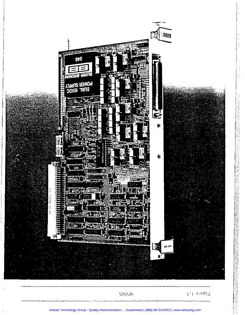
S06J\dY-; L ·L 0Jn~u
Artisan Technology Group - Quality Instrumentation ... Guaranteed | (888) 88-SOURCE | www.artisantg.com

Artisan Technology Group - Quality Instrumentation ... Guaranteed | (888) 88-SOURCE | www.artisantg.com

Chapter 1 - GENERAL INFORMATION
1.1 INTRODUCTION
This manual provides general information, installation instructions, operating instructions, functional description and applications software examples for the MPV905 analog output board (current source).
1.2 GENERAL DESCRIPTION
The MPV905 analog output board is electrically and mechanically compatible with, and interfaces directly to the VMEbus. ·
The features of the MPV905 include:-
- 8 current source output channels. - 12 bit resolution. - 3 output ranges covering standard industrial requirements. - Address block selectable in 16 Mbyte memory space.
Dynamic analog outputs (using a single digital to analog converter to drive all 8 channels) allow the MPV905 to provide high channel density on a single board. This approach frees system space for other peripherals and minimizes per channel power requirement.
Digital output data for each channel is stored in on-board RAM and the corresponding analog output voltage of the DAC is stored in separate sample and hold circuits. These circuits are continually updated by refresh circuitry. A voltage to current converter on each channel then provides the current output.
The host CPU changes data in the on-board RAM, and therefore the output current, by a write operation to the appropriate channel. Glitch free operation is ensured as the refresh circuitry is disabled while new data is being written to the RAM. At power up, all outputs are set to minimum current output for the selected range.
Address and Address Modifier (AM) decoding are jumper programmable in the 16Mbyte memory space.
An on-board DC to DC converter powers the MPV905 from the +5V system supply, the current source outputs being powered from a user supply.
... /
Artisan Technology Group - Quality Instrumentation ... Guaranteed | (888) 88-SOURCE | www.artisantg.com
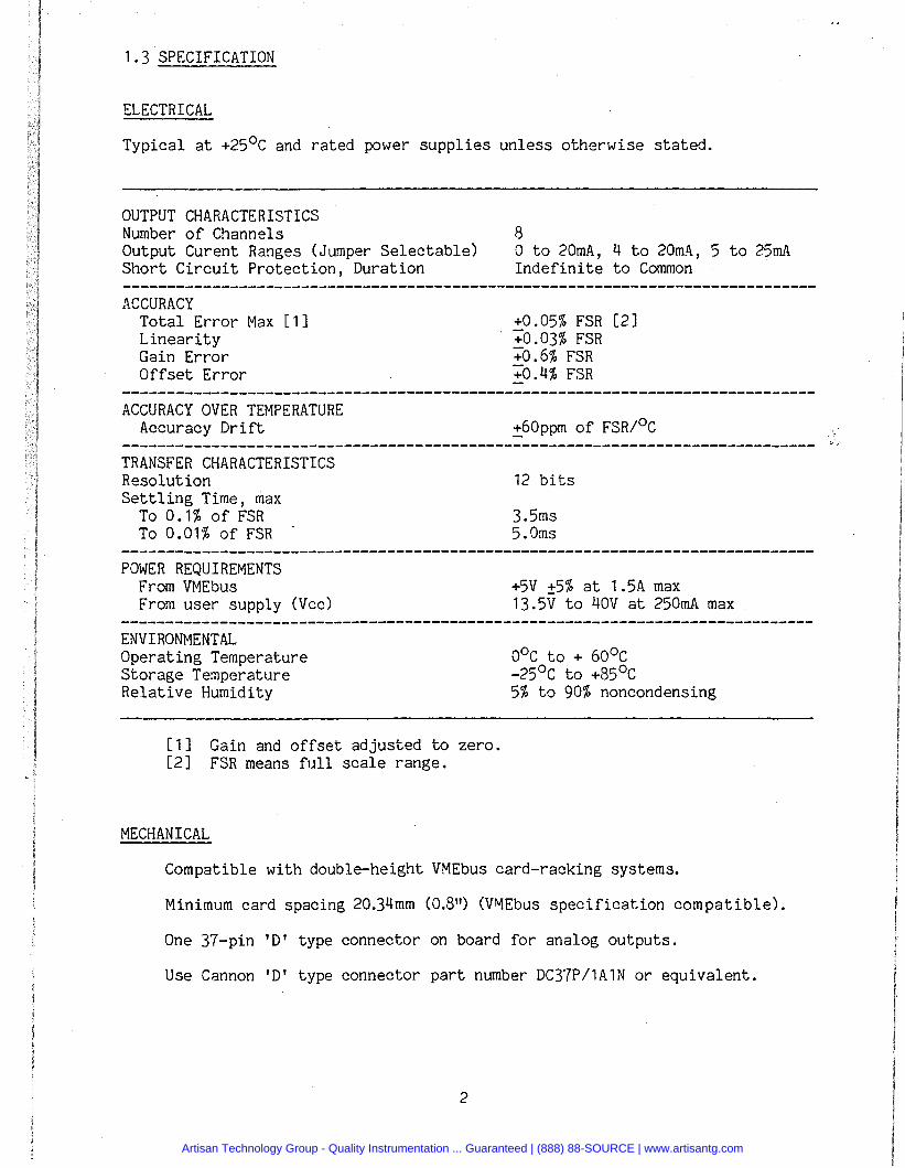
1.3 SPECIFICATION
ELECTRICAL
Typical at +25°C and rated power supplies unless otherwise stated.
OUTPUT CHARACTERISTICS Number of Channels Output Curent Ranges (Jumper Selectable) Short Circuit Protection, Duration
ACCURACY Total Error Max [1] Linearity Gain Error Offset Error
ACCURACY OVER TEMPERATURE Accuracy Drift
8 0 to 20mA, 4 to 20mA, 5 to 25mA Indefinite to Common
+0.05% FSR [2] "+0.03% FSR +0.6% FSR "+0.4% FSR
+60ppm of FSR/°C ------------------------------------------------------------------------------ ~,' TRANSFER CHARACTERISTICS Resolution Settling Time, max
To 0.1% of FSR To 0.01% of FSR
POWER REQUIREMENTS From VMEbus From user supply (Vee)
ENVIRONMENTAL Operating Temperature Storage Temperature Relative Humidity
[1] Gain and offset adjusted to zero. [2] FSR means full scale range.
MECHANICAL
12 bits
3.5ms 5.0ms
+5V +5% at 1.5A max 13.5V to 40V at 250mA max
o0 c to + 60°C -25°c to +85°C 5% to 90% noncondensing
Compatible with double-height VMEbus card-racking systems.
Minimum card spacing 20.34mm (0.8") (VNIEbus specification compatible).
One 37-pin 'D' type connector on board for analog outputs.
Use Cannon 'D' type connector part number DC37P/1A1N or equivalent.
2
Artisan Technology Group - Quality Instrumentation ... Guaranteed | (888) 88-SOURCE | www.artisantg.com

Chapter 2 - INSTALLATION INSTRUCTIONS
2.1 INTRODUCTION
This chapter provides installation instructions and an overview of the user selectable options on the MPV905.
2.2 PREPARING THE BOARD
This section describes the hardware preparation of the MPV905 prior to installation in a VMEbus system. Following the instructions described in this section will ensure that the board is configured as desired and will function as expected when installed.
MPV905 boards are factory calibrated and tested prior to shipment with> jumpers in pre-determined positions.
Figure 2.1 indicates the physical position of the jumpers on the board.
Table 2.1 lists each jumper, its function and the factory set position.
A detailed description of each jump2r is given in sections 2.2.1 through 2.2.3.
To alter the address modifier code response from the factory set values, the user must program the decoding PROM as described in section 2.2.3.1.
Before installation, the user should verify the configuration of the jumpers and, if necessary, alter the configuration to suit particular system requirements.
The board should not be installed or removed while power is applied to the VMEbus system.
3
Artisan Technology Group - Quality Instrumentation ... Guaranteed | (888) 88-SOURCE | www.artisantg.com

Figure 2.1 Position of Jumpers and Pots
RV1 Gain Adjust
RV2 Offset Adjust ~----,,--,
I I I I Channel 7 Ill ~ __ J L _ = __.
Channel 5
r---~r--1
II I ,, !_- -~L-- _j
r--1 I
Channel 3 I Ill ~ __ .J
Channel 2
Channel 1
r---, I I L __ ....J
r- -i ~--- 1 I I I 1- jll \_I L __ '-- _.
IC9 AM Response
PROM J4 Response
J3 Base Address
(A16-A23)
J2 u I r- Base Address L- (A08-A15)
J1 Base Address "·
(A04-A07)
Channel 6
--Channel 4
Spare Jumpers
Channel 0
I CHANNEL JUMPER GAIN OFFSET -------- ADJUST I ADJUST :e: l GAIN l 0 J10 RV10 RV20
110013 l ~ADJUST l 1 J 11 RV11 RV21 I I I
JUMPERS -:co: 2 I I I I 2 J12 RV12 RV22 I I I I
I 10::::0L..1 :s: OFFSET : 3 J13 RV13 RV23 11 __ 1
l -:--i ADJUST l 4 J14 RV14 RV24 I I I 5 J15 RV15 RV25 I I I I
6 J16 RV16 I RV26 I -------- 7 I I RV27 J17 I RV17 I
4
Artisan Technology Group - Quality Instrumentation ... Guaranteed | (888) 88-SOURCE | www.artisantg.com
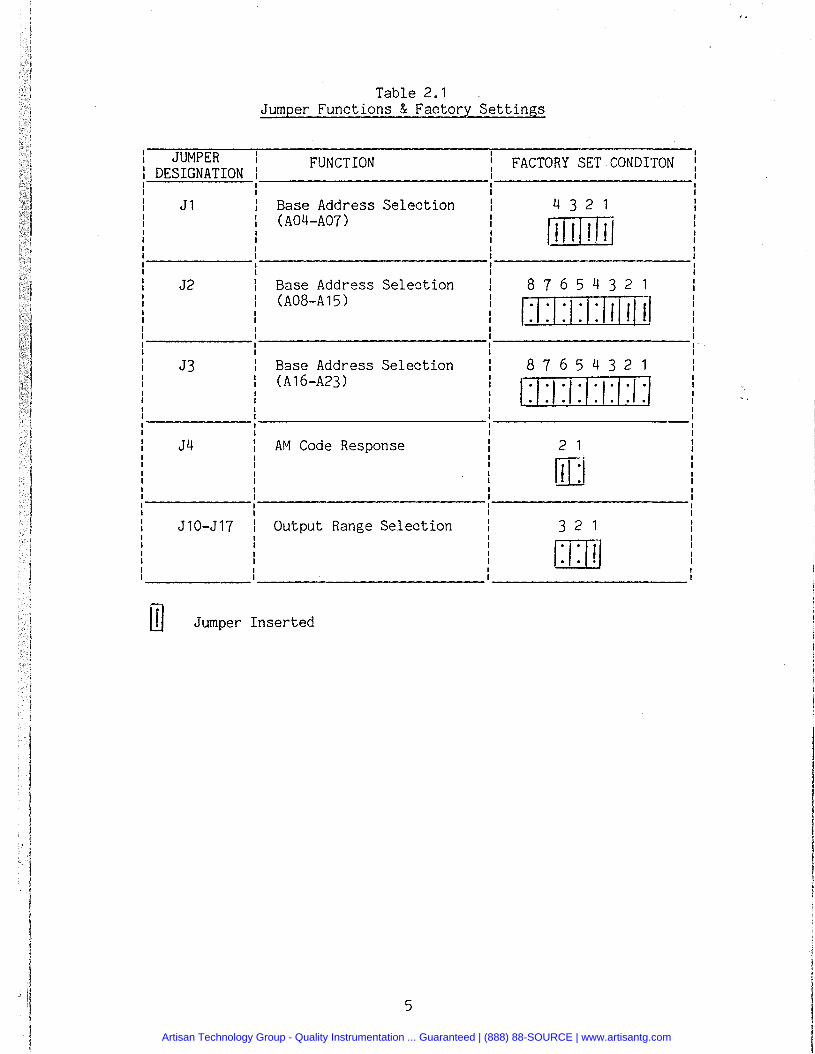
Table 2.1 Jum2er Functions & Factory Settings
JUMPER I I I FUNCTION I FACTORY SET CONDITON
DESIGNATION : I I
I I I I
J1 I Base Address Selection I 4 3 2 1 I I
(A04-A07) I
IIIIIJ.Iil I
-J2 I Base Address Selection I 8 7 6 5 4 3 2 1 I I
(A08-A15) I
1:1:1:1 :I :lfll/ fl I
J3 I Base Address Selection I 8 7 6 5 4 3 2 1 I I
(A16-A23) I
I :I :1:1 :I :1:1 :I :1 I
; "' I I I I I I I I
J4 I AM Code Response I 2 1 I I
[[J
J10-J17 I Output Range Selection I 3 2 1 I I ' em
UU Jumper Inserted
5
Artisan Technology Group - Quality Instrumentation ... Guaranteed | (888) 88-SOURCE | www.artisantg.com

2.2.1 Base Address Selection
The base address of the MPV905 can be set to any value by selecting the appropriate combination of positions on jumpers J1, J2 and J3. The factory set configuration is FFF800H. To change the sense of a bit simply change the jumper setting for that bit.
The MPV905 occupies 8 successive memory locations (word locations) within the system memory map.
Figure 2.2 shows the location and factory set configuration of the jumpers J1, J2 and J3. Table 2.2 lists the jumper positions that determine which base address is selected.
Figure 2.2 Base Address Selection Jumpers
8 7 6 5 4 3 2 1
I :I :I : I : I : I :I :I : I J3
8 8 7 6 5 4 3 2 1 c
I :I :I :I :I : I 'I ! I i I J2
4 3 2 1
lililtlil J1
Table 2.2 Base Address Jumper Selection
ADDRESS FACTORY I JUMPER LINE SET
A04 0 J1 Position 1 A05 0 2 A06 0 3 A07 0 4 A08 0 J2 Position 1 A09 0 2 A10 0 3 A 11 I 1 4 A12 I 1 5 I
A13 I 1 I 6 I
A14 I 1 7 I
A15 I 1 8 I
A16 I 1 J3 Position 1 A17 1 2 A18 1 3 A19 1 4 A20 1 5 A21 1 6 A22 I 1 I 7 A23 I 1 I 8 I I
NOTE: 0 = Jumper Inserted 1 = Jumper Removed
6
Artisan Technology Group - Quality Instrumentation ... Guaranteed | (888) 88-SOURCE | www.artisantg.com

2.2.2 Output Current Range Selection
Jumpers J10 to J17 are used to set the output current range of the analog outputs.
Each output is set at the factory for 4 to 20mA operation (complementary straight binary coding).
When changing the output current range first remove all the jumper links, then insert those required for the desired range. Table 2.3 lists the available analog output ranges and the appropriate jumper settings.
Figure 2.3 shows the factory set condition for the jumpers of all channels. Refer to Figure 2.1 for the appropriate channel and corresponding jumper number.
Figure 2.3 Analog Output Range Selection Jumper
~3
JUMPERS 2 1
Table 2.3
~ L-.1
GAIN ADJUST
OFFSET ADJUST
Analog Output Range Selection
RANGE
0 to 20rnA * 4 to 20mA
5 to 25rnA I
JUMPER SELECTION INSERT I REMOVE
2,3 1 1 '3
1 2,3 2
-=~~~~~~'--------- ---------* NOTE:- Factory Set Condition
2.2.3 Address Modifier Code Response
IC9 is a PROM, which in conjunct ion with jumper J4, positions 1 and 2, allows the response to address modifier codes to be varied to suit user requirements. The PROM/jumper combination offers the options shown in Table 2.4. The PROM program which enables this response is shown in the programming chart of Figure 2.5, at the end of this chapter.
7
!>,'
Artisan Technology Group - Quality Instrumentation ... Guaranteed | (888) 88-SOURCE | www.artisantg.com
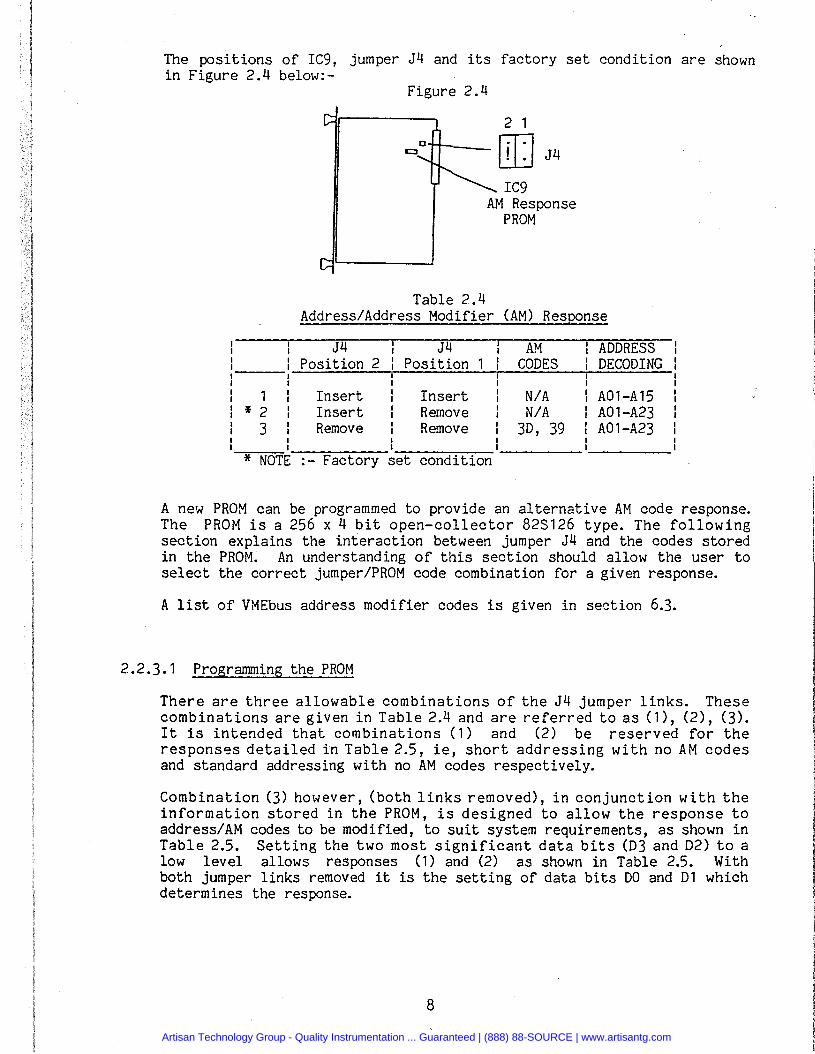
The positions of IC9, jumper J4 and its factory set condition are shown in Figure 2.4 below:-
Figure 2.4
Table 2.4
2 1
[[] J4
IC9 AM Response
PROM
Address/Address Modifier (AM) Res22nse
J4 I J4 AM I ADDRESS I I
Position 2 I Position 1 I CODES I DECODING I I I I I I I
1 I Insert I Insert I N/A I A01-A15 I I I
* 2 I Insert I Remove I N/A I A01-A23 I I I
3 I Remove I Remove I 3D, 39 I A01-A23 I I I I I I I
* NOTE :- Factory set condition
A new PROM can be programmed to provide an alternative AM code response. The PROM is a 256 x 4 bit open-collector 82S126 type. The following section explains the interaction between jumper J4 and the codes stored in the PROM. An understanding of this section should allow the user to select the correct jumper/PROM code combination for a given response.
A list of VMEbus address modifier codes is given in section 6.3.
2.2.3.1 Programming the PROM
There are three allowable combinations of the J4 jumper links. These combinations are given in Table 2.4 and are referred to as (1), (2), (3). It is intended that combinations (1) and (2) be reserved for the responses detailed in Table 2.5, ie, short addressing with no AM codes and standard addressing with no AM codes respectively.
Combination (3) ho\o~ever, (both links removed), in conjunction with the information stored in the PROM, is designed to allow the response to address/AM codes to be modified, to suit system requirements, as shown in Table 2.5. Setting the two most significant data bits (D3 and D2) to a low level allows responses (1) and (2) as shown in Table 2.5. With both jumper links removed it is the setting of data bits DO and D1 which determines the response.
8
Artisan Technology Group - Quality Instrumentation ... Guaranteed | (888) 88-SOURCE | www.artisantg.com

The following section (2.2.3.2) illustrates the method to be used when programming the PROM to produce a given response.
Table 2.5 Address/AM Response Options with Jumper Links Removed
AM CODE I DATA BIT I I RESPONSE NOTE ( 1) : D3 D2 D1 DO .
XY : 0 0 0 0 I Short addressing with AM I
XY : 0 0 0 1 I Short addressing with AM I
XY : 0 0 1 0 I Standard addressing with AM I
XY : 0 0 1 1 I No response to address/AM I I
-===~~-~~~~--~~ NOTE: The AM code indicated as XY can take any of the possible values defined in the VMEbus specification Revision B. (See Section C).
2.2.3.2 Programming Examples
The Factory Response
Referring to Table 2.4, the programming of the PROM to give the factory set response is as follows.
1. Decide upon STANDARD or SHORT addressing- STANDARD (ie, A01-A23 decoded)
2. Decide upon AM codes to which the board will respond - 3D, 39.
3. Refer to Table 2.5 and under "response" heading look for "Standard addressing with AM". The data to be stored at the relevant memory addresses can then be read from the table (in this case 0010 (02H)).
4. Place the code obtained in (3), (ie 02H), at memory locations 3D and 39.
5. Refer to Table 2.5 and under "response" heading look for "No response to address/AM". The data to be stored at the relevant memory addresses, (in this case all locations other than 3D and 39), can then be read from the table, (in this case 0011 (03H)).
6. Place the code obtained in (5), (ie, 03H), at all memory locations other than 3D and 39.
9
Artisan Technology Group - Quality Instrumentation ... Guaranteed | (888) 88-SOURCE | www.artisantg.com

Short Addressing With AM
Assume that the following response is desired - Short Address decoding, (ie, A01 -A 15 decoded) and AM codes 20 and 29* to be responded to. The following steps would yield the data to be placed in the PROM.
1. Addressing mode- SHORT.
2. Code response - 20 and 29.
3. Refer to Table 2.5 and under "response" heading look for "Short addressing with AM" (Note - there are two entries under this heading). The data to be stored at the relevant memory address can then be read from the table, (in this there is a choice of two codes - 0000 (OOH) or 0001 (01H)).
4. Place either of the codes obtained in (3), (ie, OOH or 01H), at memory locations 20 and 29.
5. Refer to table 2.5 and under "response" heading look for "No response to address/AM". The data to be stored at the relevant · memory addresses (in this case all locations other than 20 and 29), ,. can then be read from the table, (in this case 03H).
6. Place the code obtained in (5), (ie, 03H) at all memory locations other than 20 and 29.
Similar reasoning applies to any other combination of address/AM response.
*Any number and combination of AM codes may be catered for.
1 0
Artisan Technology Group - Quality Instrumentation ... Guaranteed | (888) 88-SOURCE | www.artisantg.com

;~
Chapter 3 - OPERATING INSTRUCTIONS
3.1 INTRODUCTION
This chapter provides the necessary information to allow the use of the MPV905 in a VMEbus system.
3. 1.1 Jumper Setting Checklist
Before plugging the board into a VMEsystem and applying power, check, to ensure proper system operation, that the following options have been correctly set.
1. Base Address. Has the Base Address of the board been set to suit system requirements? (Section 2.2.1)
2. Address Modifier Response. Has Address Modifier Response been correctly set? (Section 2.2.3)
3. Output Range. Has the correct current output range been selected? (Section 2.2.2)
3.2 OPERATING PROCEDURE
The board is shipped from the factory in a calibrated condition and ready for use. Installation only requires plugging the card into an empty slot in the V'1Ebus card cage and wiring the analog connector. However, the board can be adapted to suit user requirements therefore, some features of the board are jumper selectable. These features are covered in chapter 2 which should be referred to before using the board or if a configuration other than the factory set condition is desired.
3.2.1 Programming
The board is programmed as 8 successive memory locations (word locations), jumper selectable within the 16 Mbyte address range, in 8 word blocks, commencing at address OOOOOOH. The analog output has a resolution of 12-bits and therefore word accesses are required for each channel.
11
Artisan Technology Group - Quality Instrumentation ... Guaranteed | (888) 88-SOURCE | www.artisantg.com

3.2. 1.1 Address Map (Memory Map)
The address map (memory map) for the MPV905 board is shown in Figure 3.1. The base address is jumper selectable. (Section 2.2.1)
Output data (i.e. data to set an analog output to a particular value) is transferred to the board from the CPU with MOVE instructions to the appropriate addresses. 8 consecutive addresses are used, starting from the base address XXXXXO, (the X-states are selected as previously described). As each operation is a word access, word addressing must be used (even addresses only).
NOTE : A read operation to a channel results in the channel being reset to the lowest current output in the selected range. ·
Figure 3.1 MPV905 Address (Memory) Map
Factory Set WRITE READ Address D15 D11 DO D15 D11 DO FFF800l///////// OUTO l l/////////1 RESET OUTO FFF802l///////// OUT1 l l/1///////l RESET OUT1 FFF804l///////// OUT2 l l///////1/l RESET OUT2
/IIIII/I/ • l /////////' /II/IIIII • l ///////// ll/1///// . l ///////// Ill////// . l /////////
• l/11111111 l /////////. FFF80E l I I I I I I I I I OUT7 l I I I I I I I I I l--.,-RE"""s=E=T.....,O"""u=T=7---
3.2.2 CPU Instructions
The CPU transfers data to the MPV905 by using MOVE instructions, using the addresses and data lines shown in the address (memory) map of Figure 3. 1. These instructions are described in the following 1 ist. The selected base address of the board is XXXXXO (factory set to FFF800H). The CPU register Dn is used as the data register (and may be any of the allowable registers within the CPU).
MOVE. W Dn, FFF800 - This instruct ion moves the contents of data register Dn, within the CPU, to analog output OUT0.
MOVE.W Dn,FFF802 - This instruction moves the contents of data register Dn, within the CPU, to analog output OUT1.
MOVE.W Dn,FFF80E - This instruction moves the contents of data register Dn, within the CPU, to analog output OUT7.
This illustrates the procedure for transferring data to the MPV905 to allow each output to be individually set.
12
Artisan Technology Group - Quality Instrumentation ... Guaranteed | (888) 88-SOURCE | www.artisantg.com

3.2.3 Analog Output Section
3.2.3.1 Analog Output Current and Converter Input Codes
The digital input value of a selected output is converted to a current. The digital to analog converter gives an output coding scheme of complementary straight binary.
Table 3.1 illustrates the full-scale negative, mid-scale and full-scale positive output currents for the three output ranges with the corresponding digital input codes of the digital to analog converter and the value of the least significant bit (LSB).
Figure 3.2 shows, in graphical form, the relationship between the digital input code and the output current.
e.g. In Table 3.2 a digital input code of (X)FFFH corresponds to an output current of 4mA in the range 4 to 20mA. In the same range a value of (X)OOOH will produce an output current of 19.996mA.
Table 3.1 Complementary Straight Binary
SELECTED : NEGATIVE : MIDSCALE : POSITIVE 1 RESOLUTION RANGE : FULL SCALE : : FULL SCALE .
OUTPUT CODE : : (X)FFFH : (X)7FFH : (X)OOOH 0 to 20mA! O.'OOmA : +10.0mA ! +19.995mA :- 4.88uA
____ I __ _
4 to 20mA! 4.00mA : +12.0mA : +19.996mA : 3.91uA I ~------ --.-...,....,...
5 to 25mA: 5.00mA ! +15.0mA ! +24.995~~ : 4.88uA I I
NOTE:- x-indicates don't care states
Figure 3.2 Complementary Straight Binary
Output Current 25mA 20mA 20mA
5mA 4mA OmA
1 3
X)OOOH Digital Input Code
Artisan Technology Group - Quality Instrumentation ... Guaranteed | (888) 88-SOURCE | www.artisantg.com

3.2.3.2 Calculating Output Current From Input Code
The analog output current may be calculated from the input code, written by the CPU, as shown below.
Output Current = Negative Full Scale +
where,
(4095-code) x range 409
range = theoretical range of values in the selected output range. code = DECIMAL value of code placed in CPU register and written to
output (with four MSB's set to zero).
NOTE: The code consists of 12 significant bits; bits D00-D11. In the CPU register bits D12 to D15 can be set to any value before data is written to the output. However, before using the following formula, bits D12 to D15 must be set to 0 for all input codes.
e.g. consider an output range of 0 to 20mA and a code of 7FFH. Then,
range = 20mA
code = Decimal value of 7FFH = 2047
Output Current = OmA + (4095 - 2047) x 46~6 = 10mA
Referring to Table 3.1 it can be seen that for a code of 7FFH, the expected voltage is 10mA.
3.2.3.3 Output Range Selection
The analog outputs are factory set for a range of 4 to 20mA. Other output ranges can be selected as described in section 2.2.2.
3.2.3.4 Output Check
Static checks of the analog outputs can be performed by loading the memory locations with output data words. The base address XXXXXO is factory set to FFFSOOH (refer to address map Figure 3.1). The ideal values for positive and negative full scale are shown in Tables 3.1 and 3.2. The most significant four bits of the data word (D11-D15) are don't care states.
A program which performs a simple dynamic check of the analog outputs is listed in section 5.3.
14
Artisan Technology Group - Quality Instrumentation ... Guaranteed | (888) 88-SOURCE | www.artisantg.com

3.2.4 Output Calibration
Each of the analog outputs can be calibrated by means of a gain and offset adjustment as outlined below:-
Install the MPV905 in a VMEbus system and allow it to reach thermal equilibrium (about 20 minutes under power) before commencing the procedure. The positions of the calibration potentiometers are shown in Figure 2.1.
Since rnultirneters are generally more capable of accurate voltage than current measurement, it is recommended that the scheme shown in Figure 3.3 be adopted during the calibration procedure. This involves the use of a resistive load on each output of the MPV905 and the use of a rnultirneter to measure the voltage developed across the resistor in response to the current passing through it. The recommended resistance value is 500 Ohm +/-0.01% , 0.25W , T.C. of resistance 10 ppm per degree Cor better.
1. Connect a DVM (5 1/2 digit) between the appropriate output being calibrated and a return on the front panel 'D' type connector.
2. Load the appropriate memory location with the code XFFFH. (XFFEH if · 0 to 20 rnA range).
3. Adjust the appropriate offset control until the DVM reads, for the range of interest, the value indicated in Table 3.3
4. Load the appropriate memory location with the. code XOOOH.
5. Adjust the appropriate gain control until the DVM reads, for the range of interest, the value indicated in Table 3.3
6. Return to step 2 and repeat through 6 until the desired voltages are obtained.
Calibration is now complete.
15
Artisan Technology Group - Quality Instrumentation ... Guaranteed | (888) 88-SOURCE | www.artisantg.com

. : .
RANGE
0 to 20rnA 4 to 20rnA 5 to 25rnA
Figure 3.3 Recommended Calibration Method
DVM (5 1/2 DIGIT):
I I
1-1 I I I I I I I I I I T I
500 Ohm 0.01%
Table 3.3 Calibration Values
-~ --~ - T-1-.---- I I I I I I I
0 0
DATA (X)FFFH-:-DATA -(X)FFEH DATA (X)OOOH
2V +1mV 2.5V-+1mV
2. 44mV +0. 5mV 9. 9976V + 1. OmV 9.9980V +"1.0mV 12.498V ~1.0mV
3.2.5 Output Loading
1 LSB
4.88uA 3.91uA 4.88uA
The maximum load resistance into which the MPV905 will source current is dependent upon the value of the user defined external power'source. Figure 3.4 shows the relationship between load resistance and power supply (Vee on the front panel 'D' type connector).
2000
RL (Ohms) 1500
1000
500
0 . 15
Figure 3.4 Maximum RL vs Vee
Io max =
20 25
1 6
30 40----+:Vcc (Volts)
Artisan Technology Group - Quality Instrumentation ... Guaranteed | (888) 88-SOURCE | www.artisantg.com

3.3 Analog Connector
The analog front panel connector, P3, is a 37 way 'D' type socket (female). The mating connector should be a 37 way 'D' type plug (male). Use Cannon type DC37P/1A1N or equivalent.
'D' Type Connector Pinout
19 0 Vee (USER SUPPLIED) Vee (USER SUPPLIED) 0 37 18 0 Vee (USER SUPPLIED)
OV (ANALOG COMMON) 0 36 17 0 OV (ANALOG COMMON) OV (ANALOG COMMON) 0 35 16 0 OV (ANALOG COMMON) OV (ANALOG COMMON) 0 34 15 0 OV (ANALOG COMMON) OV (ANALOG COMMON) 0 33 14 0 OV (ANALOG COMMON) OV (ANALOG COMMON) 0 32 13 0 OV (ANALOG COMMON) OV (ANALOG COMMON) 0 31 12 0 OV (ANALOG COMMON) OV (ANALOG COMMON) 0 30 11 0 OV (ANALOG COMMON) OV (ANALOG COMMON) 0 29 10 0 OV (ANALOG COMMOH) OV (ANALOG COMMON) 0 28 9 0 OV (ANALOG COMMON) OV (ANALOG COMMON) 0 27 8 0 OUT4 OV (ANALOG COMMON) 0 26 7 0 OUT5 OV (ANALOG COMMON) 0 25 6 0 OUT6 OV (ANALOG COMMON) 0 24 5 0 OUT7 OV (ANALOG COMMOtJ) 0 23 4 0 OUTO OV (ANALOG COMMON) 0 22 3 0 OUT1 OV (ANALOG COMMON) 0 21 2 0 OUT2 OV (ANALOG COMMON) 0 20 1 ("'\ OUT3
3.4 Factory Set Configuration
All boards are shipped from the factory ready for immediate use, however, they do have a number of user selectable options. These options and their factory set conditions, which have already been described, are summarized below:
BASE ADDRESS . . . . . . . . . . . . . . . . . . . . . FFF800H ADDRESS/AM RESPONSE .............. STANDARD ADDRESSING/ALL AM CODES OUTPUT RANGE . . . . . . . . . . . . . . . . . . . . . 4 TO 20mA
17
Artisan Technology Group - Quality Instrumentation ... Guaranteed | (888) 88-SOURCE | www.artisantg.com

Artisan Technology Group - Quality Instrumentation ... Guaranteed | (888) 88-SOURCE | www.artisantg.com

Chapter 4 - FUNCTIONAL DESCRIPTION
4.1 INTRODUCTION
This chapter is intended to provide a background to the theory of operation for the MPV905 8 Channel analog output board. It should be read while referring to the schematics, major component data sheets (Chapter 6), and where appropriate, other chapters in this manual.
4.2 GENERAL INFORMATION
The MPV905 is a 8 channel analog current source output board with 12 bit resolution which interfaces directly to the VMEbus. Figure 4.1 shows a block diagram of the board.
4.3 THEORY OF OPERATION
The design of the fJIPV905 board is based on a dynamic output approach. This uses a single digital to analog converter (DAC) to drive all 8 outputs. Digital data for each channel is stored in the on-board RAM while analog output data for each channel is stored in separate sample and hold circuits. The control and refresh circuitry contains a channel counter that selects, from RAM, the appropriate DAC input for the channel being updated and multiplexes the DAC output to the appropriate sample and hold circuit. Thus the output data is updated independently of the CPU.
The CPU changes data in the on-board RAM by a write operation on data 1 ines DOO-D11, (DOO is the LSB), to the appropriate channel. When this occurs, the control logic disables the refresh circuitry to prevent output glitches and to allow the CPU to change the data stored in the onboard RAM.
4.3.1 Address/AM Decoder
The address decoding section consists of three eight bit magnitude comparators (IC17, IC20, and IC21). These devices monitor address bits A04 through A23 inclusive. The address modifier (AM) decoding is performed by the PROM (IC9). The operation of this section would be as follows:-
The user would insert the appropriate combination of jumper links at positions J1, J2 and J3 thus setting the base address of the board within the memory map. The jumper links at J4 (in combination with the program stored in the PROM IC9) would also be appropriately set to select the desired response to the AM codes.
18
Artisan Technology Group - Quality Instrumentation ... Guaranteed | (888) 88-SOURCE | www.artisantg.com

.--ADDRESS ...
.) MODIFIER VME bus CONTROL f- -· --·-··-
ADDRESS LOGIC ADDRESS AND AH
BUS .... DECODER
VHEbus v t -
DATA ........ VM[bus DATA
DATA BUS ....... STORAGE ... OUTPUT / K BUS RECEIVER .... RAM CONTROL CLOCK
13-5 v r "~-:,sv +ISV
~"' L--- DC TO DC f--oOV{A) ~ DIGITAL .~ -.. r -~
,./ TO ANALOG CONVERTER ~ DEHULTI' OV{D) -15V CONVERTER
-PL£xER M • CH 7
P' , r-
I' 3'
MPV 905 Block Diagram
Artisan Technology Group - Quality Instrumentation ... Guaranteed | (888) 88-SOURCE | www.artisantg.com

Upon initiation of a data transfer on the VMEbus, the levels on the address lines A04 through A23 inclusive are compared with the levels set at the jumper positions J1, J2 and J3. Only when every driven l~vel exactly matches the corresponding set level, will the three comparator outputs (P=Q) be driven to the active LOW level, indicating that the address placed on the bus matches the set address.
Similarly, with AM decoding, a recognisable A~ code on bus lines AMO through AM5 inclusive will re$ult in the PROM outputs being driven to the active LOW level. Assumin1 that the transfer is neither an interrupt cycle nor a LONGWORD cycle, IACK and LWORD are monitored to check this), then a HIGH level will appear at pin 8 of IC7. This HIGH level is an indication to subsequent control circuitry that the MPV905 should respond during the current transfer.
4.3.2 Memory Access
The data to be output is stored in the on-board RAM (IC2, IC6 and IC10) during a write cycle to the board. The memory is enabled to allow write operations to take place when the output of IC7 pin 8 is in the HIGH state. A HIGH level at this point clocks IC19, enabling bus buffers IC1 and IC5, thus allowing the data on the bus to be presented to the inputs of the RAM. Following this, the monostable (IC11 pin 1) is triggered and applies the write enable signal to the RAM thus latching (storing) the data present on the data lines DOO through 011. DTACK is then driven, through IC18, to indicate that data has been stored.
4.3.3 Timing and Control Logic
IC14, R9 and C14 form a 50kHz clock, the output of which is fed to a counter (IC15). The counter outputs are fed via IC22 to both the address inputs of the RP.:-.1 and to the address input of the demultiplexer (IC24). The counter "counts" from 0 to 7 and resets. P.s it does so, it cycles around the values stored in RAM for each of the outputs. As each location is accessed, the stored data is applied to the input of the digital to analog converter and the output of the converter is switched through the multiplexer to the appropriate output device. This process continues without interruption until a new value is written to the board. During a data write operation the clock is disabled and the counter output is frozen at the current value. The address of the memory location to be updated is fed via IC22 to the RAM address lines allowing the appropriate location to be filled with new data. At the end of the transfer, the clock is restarted and the counter again cycles around the data stored in memory.
4.3.4 Analog Output
Each of the analog outputs is a combined filter device followed by a voltage to current converter. that any glitches which occur during the switching at the output.
19
and sample-and-hold The filtering ensures process do not appear
Artisan Technology Group - Quality Instrumentation ... Guaranteed | (888) 88-SOURCE | www.artisantg.com

Artisan Technology Group - Quality Instrumentation ... Guaranteed | (888) 88-SOURCE | www.artisantg.com
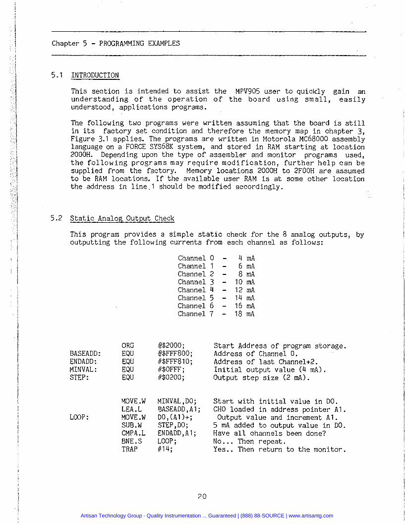
Chapter 5 - PROGRAMMING EXAMPLES
5.1 INTRODUCTION
This section is intended to assist the MPV905 user to quickly gain an understanding of the operation of the board using small, easily understood, applications programs.
The following two programs were written assuming that the board is still in its factory set condition and therefore the memory map in chapter 3, Figure 3.1 applies. The programs are written in Motorola MC68000 assembly language on a FORCE SYS68K system, and stored in RAM starting at location 2000H. Depending upon the type of assembler and monitor programs used, the following programs may require modification, further help can be supplied from the factory. Memory locations 2000H to 2FOOH are assumed to be RAM locations. If the available user RAM is at some other location the address in line,1 should be modified accordingly.
5.2 Static Analog Output Check
This program provides a simple static check for the 8 analog outputs, by outputting the following currents from each channel as follows:
ORG BASEADD: EQU ENDADD: EQU MINVAL: EQU STEP: EQU
r-tOVE.W LEA.L
LOOP: MOVE.W SUB.W CMPA.L BNE.S TRAP
Channel 0 Channel 1 Channel 2 Channel 3 Channel 4 Channel 5 Channel 6 Channel 7
4mA 6 rnA 8mA
10 rnA 12 rnA 14 rnA 16 rnA 18 rnA
@$2000; Start Address of program storage. @$FFF800; Address of Channel 0. II$FFF810; Address of last Channel+2. II$0FFF; Initial output value (4 rnA). 11$0200; Output step size (2 rnA).
MINVAL,DO; Start with initial value in DO. BASEADD , A 1 ; CHO loaded in address pointer A1. DO, (A 1 )+; Output value and increment A1. STEP,DO; 5 rnA added to output value in DO. ENDADD, A 1; Have all channels been done? LOOP; No ... Then repeat. 1114; Yes .. Then return to the monitor.
20
Artisan Technology Group - Quality Instrumentation ... Guaranteed | (888) 88-SOURCE | www.artisantg.com

5.3 Dynamic Analog Output Check
This program performs a simple dynamic check of all analog outputs. A ramp (sawtooth) waveform with amplitude plus and minus full scale and frequency approximately 30Hz will be produced at each output.
This program can be used to check correct operation of all channels.
ORG @$2000; Start address of program storage. BASEADD: EQU @$FFF800; Address of channel 0. ENDADD: EQU 11$FFF810; Address of channel 7+2. MAXVAL: EQU 11$0000; Maximum output value. MINVAL: EQU 11$0FFF; Minimum output value. STEP: EQU 11$0F; Output step size.
START: MOVE.W MAXVAL,DO; Start with maximum value in DO and CHO RAMPDOWN: LEA.L BASEADD,AO; address in AO. LOOP1: MOVE.W DO,(AO)+; Output a value then increment the
channel address in AO. CMPA.L ENDADD,AO; Have all channels been done? BNE.S LOOP1; No ... The repeat. ADD.W STEP,DO; Yes .. Then next value. CMPI MINVA.L,DO; Check for minimum output value and BLT RAMPDOWN; repeat if not done ...
RAMPUP: LEA.L BASEADD,AO; Else begin to ramp up with min value LOOP2: MOVE.W DO, (AO)+; in DO and CHO address in AO.
CMPA.L ENDADD,AO; Have all channels been done? BNE.S LOOP2; No ... Then repeat. SUB.W STEP,DO; Yes .. Then next value. CMPI MAXVAL,DO; Check for max output value and repeat BGT RAMPUP; if not done ... J~P START; Else begin again.
21
Artisan Technology Group - Quality Instrumentation ... Guaranteed | (888) 88-SOURCE | www.artisantg.com

Chapter 6 - SUPPORT INFORMATION
6.1 COMPONENTS LIST
COMPONENT I DESCRIPTION DESIGNATION I
I I
R1 I Resistor Metal Oxide 27K 2% 0.25W R2 : Resistor Metal Oxide 2K2 10% 0.25W R3 I Resistor Metal Oxide 2K2 10% 0.25W R4 Resistor Metal Oxide 4K7 2% 0.25W R5 Resistor Metal Oxide 2K2 10% 0.25W R6 Resistor Metal Oxide 2K2 10% 0.25W R7 Resistor Metal Oxide 1M 10% 0.25W R8 Resistor Metal Oxide 2K2 10% 0.25W R9 Resistor Metal Oxide 910R 10% 0.25W R10 Resistor Metal Oxide 2K2 10% 0.25W R11 Resistor Carbon Film 6M8 10% 0.25W R12 : Resistor Metal Oxide 22R 2% 0.25W R13 I Resistor Metal Oxide 51K 2% 0.25W R14 I Resistor Metal Oxide 24R 2% 0.25\~ R15 I Resistor Metal Oxide 24R 2% 0.25W Rl6 I Resistor Metal Oxide 51K 2% 0.25W R17 I Resistor Metal Oxide 24R 2% 0.25W R18 I Resistor Metal Oxide 51K 2% 0.25W R19 I Resistor Metal Oxide 51K 2% 0.25W R20 I Resistor Metal Oxide 24R 2% 0.25W R21 I Resistor Metal Oxide 33K 2% 0.25W R22 Resistor Metal Oxide 33K 2% 0.25W R23 Resistor Metal Oxide 33K 2% 0.25W R24 Resistor Metal Oxide 33K 2% 0.25W R25 Resistor Metal Oxide 24R 2% 0.25W R26 Resistor Metal Oxide 51K 2% 0.25W R27 Resistor Metal Oxide 22R 2% 0.25W R28 Resistor Metal Oxide 22R 2% 0.25W R29 Resistor Metal Oxide 22R 2% 0.25W R30 Resistor Metal Oxide 22R 2% 0.25W R31 Resistor Metal Oxide 33K 2% 0.25W R32 Resistor Metal Oxide 33K 2% 0.25W R34 Resistor Metal Oxide 33K 2% 0.25W R35 Resistor Metal Oxide 33K 2% 0.25W R36 Resistor Metal Oxide 24R 2% 0.25W R37 Resistor Metal Oxide 51K 2% 0.25W R38 Resistor Metal Oxide 24R 2% 0.25W R39 I Resistor Metal Oxide 51K 2% 0.25W R40 : Resistor Metal Oxide 24R 2% 0.25W R41 I Resistor Metal Oxide 51K 2% 0.25W
I I
RV1-RV18 I Variable Resistor 100K 20 Turn Top Adjust
Artisan Technology Group - Quality Instrumentation ... Guaranteed | (888) 88-SOURCE | www.artisantg.com

COMPONENT DESIGNATION
C1-C13 C14
C15-C20 C21 C22 C23 C24 C25 C26 C27 C28 C29 C30 C31 C32 C33 C34 C35 C36 C37 C38 C39 C40 C41 C42 C43 C44 C45 C46 C47 C48 C49 C50 C51 C52 C53 C54 C55 C56 C57 C58 C59 C60 C61 C62 C63 C64 C65 C66 C67
DESCRIPTION
Capacitor Ceramic Z5U 0. 1uF 50V 20% Capacitor Polypropylene 0.01uF 63V 10% Capacitor Ceramic Z5U 0.1uF 50V 20% Capacitor Tanatalum Tap 10uF 35V 20% Capacitor Ceramic Z5U 0. 1uF 50V 20% Capacitor Tanatalum Tap 10uF 35V 20% Capacitor Ceramic Z5U 0. 1uF 50V 20% Capacitor Tanatalum Tap 10uF 35V 20% Capacitor Tanatalum Tap 10uF 35V 20% Capacitor Ceramic Z5U 0.1uF 50V 20% Capacitor Tanatalum Tap 10uF 35V 20% Capacitor Ceranic Z5U 0. 1uF 50V 20% Capacitor Tanatalum Tap 10uF 35V 20% Capacitor Ceramic Z5U 0.1uF 50V 20% Capacitor Tanatalum Tap 10uF 35V 20% Capacitor Ceramic Z5U 0.1uF 50V 20% Capacitor Polypropylene 68000pF 63V 10% Capacitor Polypropylene 68000pF 63V 10% Capacitor Tanatalum Tap 10uF 35V 20% Capacitor Ceramic Z5U 0.1uF 50V 20% Capacitor Tanatalum Tap 10uF 35V 20% Capacitor Ceramic Z5U 0.1uF 50V 20% Capacitor Polypropylene 68000pF 63V 10% Capacitor Polypropylene 68000pF 63V 10% Capacitor Polypropylene 68000pF 63V 10% Capacitor Polypropylene 68000pF 63V 10% Capacitor Tanatalum Tap 10uF 35V 20% Capacitor Ceramic Z5U 0. 1uF 50V 20% Capacitor Tanatalum Tap 10uF 35V 20% Capacitor Ceramic Z5U 0. 1uF 50V 20% Capacitor Polypropylene 68000pF 63V 10% Capacitor Polypropylene 68000pF 63V 10% Capacitor Ceramic Z5U 0.1uF 50V 20% Capacitor Tanatalum Tap 10uF 35V 20% Capacitor Ceramic Z5U 0. 1uF 50V 20% Capacitor Tanatalum Tap 10uF 35V 20% Capacitor Polypropylene 68000pF 63V 10% Capacitor Polypropylene 68000pF 63V 10% Capacitor Tanatalum Tap 10uF 35V 20% Capacitor Ceramic Z5U 0.1uF 50V 20% Capacitor Polypropylene 68000pF 63V 10% Capacitor Polypropylene 68000pF 63V 10% Capacitor Polypropylene 68000pF 63V 10% Capacitor Polypropylene 68000pF 63V 10% Capacitor Polypropylene 63000pF 63V 10% Capacitor Polypropylene 68000pF 63V 10% Capacitor Tanatalum Tap 10uF 35V 20% Capacitor Ceramic Z5U 0. 1uF 50V 20% Capacitor Tanatalum Tap 10uF 35V 20% Capacitor Ceramic Z5U 0.1uF 50V 20%
Artisan Technology Group - Quality Instrumentation ... Guaranteed | (888) 88-SOURCE | www.artisantg.com
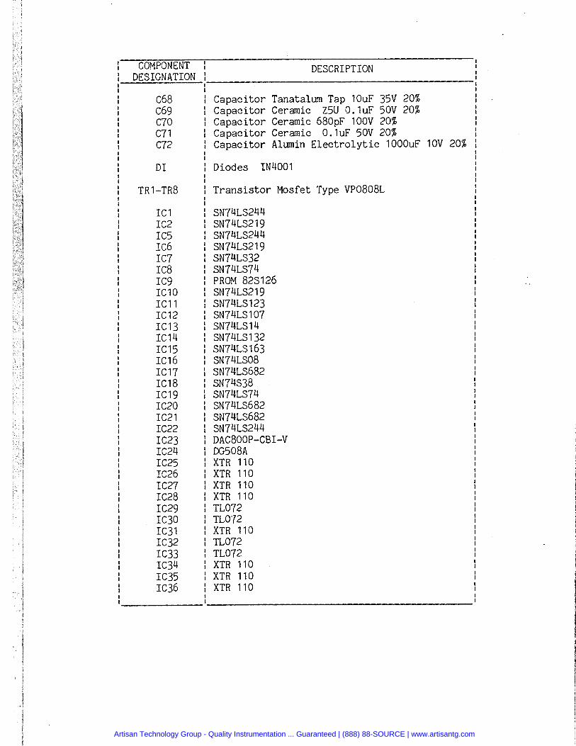
COMPONENT DESIGNATION
DESCRIPTION
C68 : Capacitor Tanatalurn Tap 10uF 35V 20% C69 : Capacitor Ceramic Z5U 0. 1uF 50V 20% C70 : Capacitor Ceramic 680pF 100V 20% C71 : Capacitor Ceramic 0. 1uF 50V 20% C72 : Capacitor Alurnin Electrolytic 1000uF 10V 20%
DI
TR1-TR8
IC1 IC2 IC5 IC6 IC7 res IC9 IC10 IC11 IC12 IC13 IC14 IC15 IC16 IC17 IC18 IC19 IC20 IC21 IC22 IC23 IC24 IC25 IC26 IC27 IC28 IC29 IC30 IC31 IC32 IC33 IC34 IC35 IC36
Diodes IN4001
Transistor Mosfet Type VP0808L
SN74LS244 SN74LS219 SN74LS244 SN74LS219 SN74LS32 SN74LS74 PROM 82S126 SN74LS219 SN74LS123 SN74LS107 SN74LS14 SN74LS132 SN74LS163 SN74LS08
I SN74LS682 SN74S38 SN74LS74 SN74LS682 SN74LS682 SN74LS244 DAC800P-CBI-V DG508A XTR 110 XTR 110 XTR 110 XTR 110 TL072 TL072 XTR 110 TL072 TL072 XTR 110 XTR 110 XTR 110
Artisan Technology Group - Quality Instrumentation ... Guaranteed | (888) 88-SOURCE | www.artisantg.com

Artisan Technology Group - Quality Instrumentation ... Guaranteed | (888) 88-SOURCE | www.artisantg.com

P3
:r,, ~
1~~R5 ~ l--· ---. _ ____j tij ~~~~121'1~,lliffi
~ ~TR8 0'2 Dl u~ C~6 -+<.JJ!, I 2' ~ ~ TR7 --{0- -a::::J- ~FI c---:-.:lC.,_,.26..,...-....,, iii a. ~TR'- ~ e llt-~Z~ Ill-~,, ll' 'I(T~IIO c:::::J TR? C.b~ .l\~ ~~ · · -CJ r.B;, ~c EEill ~ ~ c lt~ffl @ I~~ Z7j Rvl,r I
cb8+U ~ ~ 6'\- ~ ~ ri0 -+()~ d~ :I"\u
p XT'H~ I~ r Jf>?.fo I 1# p xMio I ~ .~ X~~~ I <{)&, ID!lil i3il IQ"'i'"" I 1"' 22 1"'·~ I I '""I"''' I ~:·~~~~ ~V ~i~:i 1~
1~1~1 = --f!iT& i""'-i2f•'-l ~~~~~ ~VcA)
~ FllCffi ~~ l~ 1D~~I JP~ll
~ 1~ lc~ Jc~]C~~l ---fi:ID- --rn:o- 1c'f8jcq.2jc'f<> jc,.._l
--ann- --c:!ID~
I rc~~ 9 b,A,C. 600 J'l. J
6Q' 6' 11 m ~o oe o~; m 'DC ·I>C
C:OI-lVf:RTf:IC!
~~ o.J\J ~~ -illfr-
--m!}-
EJEJ =fm: m () 0 0 Ci2 C:.6 C't
I~ I I~ I~ I~ -< 0 b1P2~ ~ ~ TP -~ 0 Cl~ tJ. ~ u 't ~f ~$ '*" ... ,.. .... .... ~
r ~
1P6 ~P5 OC:._I_I cf1 IT 3
1
~ 5
~~~ nt~ ~~ =~ l..h ~ u; Q~ ~~ ~~ ~ 0
TPI CIO C"" C2
~ 10~ .c;:, ,o ~ " cO~ Q~ 1-t~l 1ft.~
:t- c-.1 ,... t!' ,.. u~
~
ci~: ~ v ~ De.·~ ADDIU;~~ 5f::L!:c.T
~ tf'Ol .lrc:n 1
"' I~ ~!1 ... ,... TP~ C)C.? C)CI
~OC)C9
~~~~~ t= I
~-OTPIO
Orp~
OTPa 0TP7
~
Oc.n ~a J't -------- -----·-------
PI
0'1 . N
OJ 0 )> ;o 0
r )> -< 0 c: ----i
Artisan Technology Group - Quality Instrumentation ... Guaranteed | (888) 88-SOURCE | www.artisantg.com

Artisan Technology Group - Quality Instrumentation ... Guaranteed | (888) 88-SOURCE | www.artisantg.com

Table 2.9 Address Modifier Codes
--r-I
HEX I ADDRESS MODIFIER I FUNCTION I DEFINED I I I
CODE I 5 4 3 2 1 0 I FUNCTION I BY I I I I I I I
3F I H H H H H H I Standard Addressing Supervisory I VMEbuSSpec:-I I I
Ascending Access 3E I H H H H H L I Standard Addressing Supervisory I VMEbus Spec. I I I
Program Access 3D I H H H H L H I Standard Addressing Supervisory I VMEbus Spec. I I I
Data access 3C I H H H H L L I Undefined I Reserved I I I
38 I H H H L H H I Standard Addressing Non-Privil. I VMEbus Spec. I I I
Ascending Access I .,, I
3A I H H H L H L I Standard Addressing Non-Privil. I VMEbus Spec. I I I
Program Access 39 I H H H L L H I Standard Addressing Non-Privil. I VMEbus Spec. I I I
Data access 38 I H H H L L L I Undefined I Reserved I I I
30-37 I H H L X X X I Undefined I Reserved I I I
2F I H L H H H H I Undefined I Reserved I I I
2E I H L H H H L I Undefined I Reserved I I I
2D I H L H H L H I Short Addressing Supervisory I VMEbus Spec. I I I
I/0 Access 2C I H L H H L L I Undefined I Reserved I I I
28 I H L H L H H I Undefined I Reserved I I I I
2A I H L H L H L I Undefined I Reserved I I I
29 I H L H L L H I Short Addressing Non-Privileged I VMEbus Spec. I I I
I/0 Access 28 I H L H L L L I Undefined I Reserved I I I
20-27 I H L L X X X I Undefined I Reserved I I I
10-1F I L H X X X X I Undefined I Reserved I I I
OF I L L H H H H I Extended Supervisory Ascending I VMEbus Spec. I I I
Access OE I L L H H H L I Extended Supervisory Program I VMEbus Spec. I I I
Access OD I L L H H L H I Extended Supervisory Data I VMEbus Spec. I I I
Access oc I L L H H L L I Undefined I Reserved I I I
08 I L L H L H H I Extended Non-Privileged I VMEbus Spec. I I I
Ascending Access OA I L L H L H L I Extended Non-Privileged Program I VMEbus Spec. I I I
Access 09 I L L H L L H I Extended Non-Privileged Data I VMEbus Spec. I I I
Access 08 I L L H L L L I Undefined I Reserved I I I
00-07 I L L L X X X I Undefined I Reserved I I I I I I
-------~------------------I I -------------
Artisan Technology Group - Quality Instrumentation ... Guaranteed | (888) 88-SOURCE | www.artisantg.com

NOTES:
Address Modifier Codes (Cont'd)
Short address uses 15 address lines (A01-A15) Standard address uses 23 address lines (A01-A23) Extended address uses 31 address lines (A01-A31)
Codes defined by the ''VMEbus Spec." should not be used for purposes othe than those specified.
Codes defined by "User'' may be used for any purpose which the VMEbus user (board vendor or customer) deems appropriate (page switching, memory protection, MASTER or task identification, privileged access to resources, etc.,).
Codes defined by "Reserved" should not be used by the user;c, they are reserved for system use and future enhancements.
2
Artisan Technology Group - Quality Instrumentation ... Guaranteed | (888) 88-SOURCE | www.artisantg.com

BURR-BROWN®
I• II •I DAC800 DAC800P
Integrated Circuit DIGITAL-TO-ANALOG CONVERTER
FEATURES • LOW COST HIGH RELIABILITY SINGLE-CHIP
REPLACEMENT FOR INDUSTRY STANDARD DACBO
• 12-BIT RESOLUTION
• ±1/2LSB MAXIMUM NONLINEARITY, oo C to +70° C
• GUARANTEED MONOTONICITY. ooc to +70°C
• DUAL-IN-LINE PACKAGE WITH INDUSTRY STANDARD (DACBO) PINOUT
• HERMETIC PACKAGE (optional)
• TWO PACKAGE OPTIONS: hermetic side-brazed and molded plastic
• GUARANTEED SPECIFICATIONS WITH ±12V AND ±15V SUPPLIES
DESCRIPTION The DAC800 is a third-generation monolithic Integrated Circuit that is a pin-for-pin equivalent to the industry-standard DAC80 first introduced by Burr-Brown. It has all of the functions of its predecessor plus faster settling time and enhanced reliability because of its monolithic construction.
The current output model of the DAC800 is a singlechip integrated circuit containing a subsurface zener reference diode, high speed current switches, and laser-trimmed thin-film resistors. The DAC800 provides output voltage ranges of ±2.5V. ±5V, ±lOY, 0 to +5V. 0 to +IOV (V models) or output current ranges of ±1.175mA or 0 to -2.35mA (I model).
This high accuracy converter offers a maximum nonlinearity error of± I I 2LSB. ±JOppmi''C max-
imum gain drift and guaranteed monotonicity, all over0°C to +70°C. In the bipolar configuration, total drift is guaranteed to be Jess than 25ppm of FsRrc. The DAC800 is in a 24-pin dual-in-line package with the popular DAC80 pinout. Two package options ·~·. are available: a hermetic ceramic side-brazed package and a low-cost molded plastic package (voltage out only).
For designs that require a wide temperature range, see Burr-Brown models DAC850 and DAC851.
"" ... ::::> a. :!: _, • ... c; c;
VOLTAGE MODEL
6.3V REF OUT
GAIN ADJUST
•Vee
COMMON
SUMMING JUNCTION
20VRANGE
IQV RANGE
BIPOLAR OFFSET
REF INPUT
VouT
·Vee
LOGIC SUPPLY
PaleniS pend•ng may apply upon 1he allowance and issuance of palenls thereon. The product may also be covered in other countries by one or more intcrnalional patc::nts.
lnlerniltionill Airport lndustriill Park. P.O. Box t 1400 ·Tucson. Arizona 85734 ·Tel. 16021 746- tIll ·Twx: 910.952-1111 ·Cable: BBRCORP · Telex: 66-6491
C l~l<~ Hurr-Brt•v.n Ct•rpnr;tiHtn l'l>S-l40<. Pronlcd in U.S.A. March. 1984
Artisan Technology Group - Quality Instrumentation ... Guaranteed | (888) 88-SOURCE | www.artisantg.com

SPECIFICATIONS ELECTRICAL Typ1ca1 at +25"C and i Vee - 12V or 15V unless otherw1se noted.
MODEL DACSOO, DACSOOP
PARAMETER MIN TYP MAX UNITS
DIGITAL INPUT Resolulion 12 bits Logic Levels
(over spec_ temp range)'"
v~ (L09ic "1") +2 16.5 voc y._ (LI)9ie "0") 0 +0.8 VDC 1~ (V~ = +2.4V) +20 pA 1._ (Vw = +0.4V) -0.36 mA
ACCURACY linearity Error at 2s•c ±114 ±112 LSB Differential Linearity Error ±112 +1, -314 LSB Gain Error~ ±0.1 ±0.3 % Offset Error1 ~"~ ±0.05 ±0.15 %oiFSR"'
POWER SUPPLY SENSmVITY +15V and +5V Supplies ±0.0001 ±0.001 %of FSRI'J!.Va: -15VSupply ±0.003 ±0.006 %of FSRI'J!.Va:
DRIFT'~(o·c to +1o•c1 Bipolar Drill (±lull scale drift
tor the bipolar connection) ±10 ±25 ppmoiFSRrC Total error over o•c to +7«r-Cca.
Unipolar ±0.06 ±0.15 %o1FSR Bipolar ±0.05 ±0.12 %o1FSR
Gain ±10 ±30 pprni"C Unipolar ONset ±1 ±3 ppmoiFSRrC Bipolar ONset ±7 ±15 ppmoiFSRrC Oit1erential Linearity o• C to + 10• C ±112 +1, -7/8 LSB Linearity Error o• C to + 10• C ±112 LSB Mono1onic1ty Temp. Range. min 0 +70 •c
CONVERSION SPEED, V models Sellling Time to ±0.01% of FSR
For FSR Change 20V range, 2k0 load 3 5 psec 10V range, 2k0 load 2,5 4 pSec
For 1LSB Change. Major Carry, 2k0 load 1.5 pSee
Slew Rate, 2k0 load 10 15 V/pSec
CONVERSION SPEED. I model (DAC800 only)
Sellling Time to ±0.01% of FSR For FSR Change_
100 to 1000 load 300 nsec 1k0 load 1 snec
ANALOG OUTPUT, V models Ranges (=Vee = 15V) .. r2.5, ±5. :t10. 0 to +5, 0 to +10 v Outpul Current ±5 mA Output Impedance (OC) 0.05 0 Shor1 Circuit to Common. Duration Indefinite
ANALOG OUTPUT. I model (DAC800 only)
Ranges: Bipolar ±0.88 ±1.175 ±1.47 mA Unipolar 0 to -1.76 0 to -2.35 0 to -2.94 mA
Output Impedance: Bipolar 3.1 kO Unipolar 7.2 kO
Compl•ance -2.5 +2.5 v REFERENCE VOLTAGE OUTPUT .. 6.23 +6.30 +6.37 v Current (tor external loads). Source 1.5 2.5 mA Tempco of Onft ±10 !:30 ppmrc
POWER SUPPLY REQUIREMENTS %Vee :t11.4 :t15 ±16.5 voc
Voo ...
1"4.5 +5.0 +16.5 VDC Supply Drain
.. 15V. -15V (no load) +8 .. 20 +12, -25 mA 85V (11)9•C supply) +7 +10 mA
TEMPERATURE RANGE Specification 0 +70 ·c Operating'., -25 +85 ·c Storage. -60 +100 ------'- ·c
The inlormatoon in this publication has been carefully checked and is believed to be reliable; however, no responsibility is assumed for possible inaccuracies or omissions. Prices and specifications are subject to change without notice. No patent rights are granted to any of the circuits described herein.
MECHANICAL
DACSOO I"" r:·--· ... ") 13
.I ' ' .
NOTE: Leads in true position within 0.010'" (0.25mm 1 ~
1 r .. 1\ ~~· ~~.-~~-~~·~]
1.1 l L j J 12
A at MMC at seating plane.
~ u u u u u ~ I
L ..... . A F JL j
Pin numbers shown for reference on!y. Numbers may not be marked on package.
kage
.. -·- N-1--·~ £ mtm1111f- l.
I , K J
Lj__ D J : S~ting I I ~:
.J H - G'-- Plane .._ l
I I ... v .JM
DIM
A
c D F
G H
J K L
M
N
OIM
A
B c D F
G H J K
L M N
NOTES:
INCHES
MIN MAX
1.18~ 1.215
.105 .170 .015 .021 .035 .060
.100 BASIC
.03o I .o1o
.OOtl I .o12
.120' .240 .600BASIC
- I 10" .025 I .060
MILLIMETERS
MIN I t.IAX
30.10 I 30.811 2.67 I 4.32
0.38 I 0.53 o.e9 I 1.52
2.5<1 BASIC
0.761 1.78
o2o 1 o.Jo 3.05-1 6.10
1524 BASIC
- I 100 0.64 I 1.52
CASE: Ceramic MATING CONNECTOR:
0245MC
WEIGHT: 4.1 grams (0.15 OZ.)
DACSOOP
•0000000000001
I 'l . I IJ tJ (j () (j () (j tJ (j () () (] []
NOTE: Leads in true position within 0.010" (0.25mm) A at MMC at seating plane.
j,J \ -~~ .
IN( HE$
MI .... MAX
1.233 1.283
.638 .875 .1811 .224 .015 .023
.043 .082
.100 BASIC .030 .OliO
.oo81 .o 16 .1DO .132
.800 BASIC o• 15•
.0181 .022
Mll.t.IMfHR$
MI .... MA>
31.32 32.611
13.87 14.81 4.211 5.811 0.38 0,68 1.011 1.57
2.54 BASIC 0.78f 2.211
0.201 0.38 2.64 '3.35
15.24 BASI~l o• 1 1s•
0.48 o.58j
CASE: Plastic MATING CONNECTOR:
0245MC WEIGHT: 3.7 grams
(0.13 OZ.)
(1) Refer to Logic Input Compatibility section. (2) Adjustable to zero with external trim potentiometer. (3) FSR means "Ful! Scale Range" and is 20V for :t10V range, 10V for ±5
range. etc. (4) To maintain drift spec internal feedback resistors must be used lor!
current output models. (5) Includes the effects of gain. offset and linearity drift. Gain and ollse
errors are adjusted to zero at +25" C. (6) A minimum of ±13V supply is required for ±10V and 0 to 10\' ranges
All other ranges accept ±12V supplies. (7) Power dissipation 1s an additionaltOOmW, max. when Voo is operated
at +15V. (8) Max operating temperature for OACBOOP-CBI-V is +70"C
Artisan Technology Group - Quality Instrumentation ... Guaranteed | (888) 88-SOURCE | www.artisantg.com
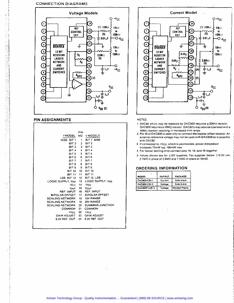
CONNECTION DIAGRAMS
Voltage Models
PIN ASSIGNMENTS
PIN I MODEL NO
MSB BIT 1 1 BIT 2 2 BIT 3 3 BIT 4 4 BIT 5 5 BIT 6 6 BIT 7 7 BIT 8 8 BIT 9 9
BIT 10 10 BIT 11 11
LSB· BIT 12 12 LOGIC SUPPLY. Voo 13
-Vee 14
lour 15 REF. INPUT 16
BIPOLAR OFFSET 17
SCALING NETWORK 18 SCALING NETWORK 19 SCALING NETWORK 20
COMMON 21 +Vee 22
GAIN ADJUST 23 6.3V REF. OUT 24
9 •Vee
Ill 1DMliJ1Dkll ~to
151 r:OOktt D.Dl,.f ·Vee
I~ 1Dk!l • ' to ~ .. lOOk!!
V MODELS
BIT 1 MSB BIT 2 BIT 3 BIT 4 BIT 5 BIT 6 BIT 7 BIT 8 BIT 9 BIT 10 BIT 11 BIT 12 LSB LOGIC SUPPLY. Voo
-Vee Vour REF. INPUT BIPOLAR OFFSET 10V RANGE 20V RANGE SUMMING JUNCTION COMMON +Vee GAIN ADJUST 6.3V REF OUT
Current Model
NOTES.
·Vee
lllku to
IOOkll
1 DAC80 wh1ch may be replaced by DAC800 requires a 33Mll resistor. DAC800 requires a 10M f.! resislor DACao·s may also be opera led w11h a 10M! I resistor resulting m increased trim range.
2. Pin 16 of DAC800 1s used only to connect the bipolar offset resislor. An external reference voltage may not be used with DAC800 as is possible With OAC80.
3. If connected to +Vee. which is permissible. power dissipation increases 75mW typ. 100mW max.
4. For faslest settling time connect pins 19. 18. and 15 together.
5 Values shown are for ±15V supplies. For supplies below -:=13.5V use 2.7MO m place of 3.9MO and 7 5MO in place of 10m0.
ORDERING INFORMATION
MODEL OUTPUT PACKAGE
OAC800-CBI·I Curren I Side-braze
DAC800-e81-V Vol! age S1de-br1ze
OAC800P-C81-V Vollage Molded Plastic
Artisan Technology Group - Quality Instrumentation ... Guaranteed | (888) 88-SOURCE | www.artisantg.com

DISCUSSION OF SPECIFICATIONS DIGITAL INPUT CODES
The DAC800 accepts complementary binary digital input codes. The CBI model may be connected by the user for any one of three complementary codes: CSB. CTC. or COR.
TABLE I. Digital Input Codes.
DIGITAL INPUT ANALOG OUTPUT
CSB COB CTC" Com pl. Com pl. Com pl.
MSB LSB Straight Offset Two's
l l Binary Binary Com pl.
000000000000 +Full Scale +Full Scale ·1LSB
011111111111 +1/2 Full Scale Zero -Full Scale
100000000000 112 Full Scale ·1LSB ·1LSB +Full Scale
111111111111 Zero -Full Scale Zero
"Invert the MSB of the COB code with an external in•·erter to obtain CTC code.
ACCURACY
Linearity of a D/ A converter is the true measure of its performance. The linearity error of the DAC800 is specified over its entire temperature range. This means that the analog output will not vary by more than ±l/2LSB, maximum, from an ideal straight line drawn between the end points (inputs all"l"s and all "O"s) over the specified temperature range of 0°C to + 70"C.
Differential linearity error of a D/ A converter is the deviation from an ideal I LSB voltage change from one adjacent output state to the next. A differential linearity error specification of ±I 1 2LS B means that the output voltage step sizes can range from I/2LSB to 3/2LSB when the input changes from one adjacent input state to the next.
Monotonicity over a 0°C to +70°C range is guaranteed in the DAC800 to insure that the analog output will increase or remain the same for increasing input digital codes.
DRIFT
Gain Drift is a measure of the change in the full scale range output over temperature expressed in parts per million per uc (ppmtC). Gain Drift is established by: I) testing the end point differences for each DAC800 model at O"C. +25"C and +70"C: 2) calculating the gain change with respect to the +25"C value and: 3) dividing by the temperature change. This figure is expressed in ppm/uC.
Offset Drift is a measure of the change in output with all "l"s on the inputs over the specified temperature range. The Offset is measured at O"C. +25"C and +70"C. The maximum change in Offset is referenced to the Offset at +25"C and is divided by the temperature change. This drift is expressed in parts per million of full scale range per "C (ppm of FSRt"C).
Bipolar Drift is a measure: of the change in plus or i1'tinus full scale: output o\'er the specification temperature range for the: bipolar connection. Because Bipolar {)ffsc:t Drift and (iain Drift have canceling interactions. Bipolar Drift is not simply the sum of the t Wtl. Tow! hi polar error ovc:r tc:mpc:rature is calculated using Bipolar Drift. then adding± I; 2LSH of linearity error.
SETTLING TIME
Settling time is the total time (including slew time) required for the output to settle within an error band around its final value after a change in input (see Figure I).
Voltage Output Models: Three settling times are specified to ±0.01% of full scale range (FSR); two for maximum full scale range changes of20V, IOV. and one for a I LSB change. The ILSB change is measured at the major carry (0 111 ... 11 to 1000 ... 00). the point at which the worst case settling time occurs.
Current Output Model: Two settling times are specified to ±!).01% of FSR. Each is given for the current model connected with two different resistive loads: 100 to 1000 and IOOOO.Internal resistors are provided for connecting a nominal load resistance of approximately IOOOQ for output voltage ranges of± IV and 0 to -2V. ·
I ' _1\JIII !!!!I v Models JJ~
# 1 l.l~ ~~
1 M;del~ ~ lOki! Feedback jl
' II _..L J I I II '0 ., ~ g' 0.3
[I) .. ~a: 0 .,
l\ I J I!''· ! !.1 .5 ~ 0.1 .,en :> = - :> ~ u. 0.03
l1 ~...-sk\1 Feedb~ck I i j iii
~ l, ~ Iii coO c -·- c u. .,
~ 0.01 ., ,~,~ ~~II '~ ·t-t-t1Ttt11
f' 'L"~ l Q.
0.003
0.001 0.1
~ "!!! RL=1011 ·' ~ to 1100111 1 ~1'-r-..br. ~r--..r-..,
10
Settling Time '~'sec·
100
FIGURE I. Full Scale Range Settling Time vs Final Value Error Band.
COMPLIANCE
Compliance voltage is the maximum voltage swing allowed on the current output node in order to maintain specified accuracy. The maximum compliance voltage of all current output models is -2.5V to +2.5V.
POWER SUPPLY SENSITIVITY
Power supply sensitivity is a measure of the effect of a power supply change on the D/ A converter output. It is defined as a percent of FSR per percent of change in either the positive. negative. or logic supplies ahout the nominal power supply voltages (sec Figure 2).
Artisan Technology Group - Quality Instrumentation ... Guaranteed | (888) 88-SOURCE | www.artisantg.com

For bipolar (COH. CTC) configurations. apply the digital input code that should produce the maximum negative output voltage and adjust the Offset potentiometer for minus full scale voltage. Example: If the Full Scale Range is connected for 20V. the maximum negative output voltage is -IOV. See Table II for corresponding codes and the Connection Diagrams for offset adjustment connections. Offset should be adjusted prior to gain.
Gain Adjustment: For either unipolar or bipolar configurations, apply the digital input that should give the maximum positive voltage output. Adjust the Gain potentiometer for this positive full scale voltage. See Table II for positive full scale voltages and the Connection Diagrams for gain adjustment connections.
TABLE II. Digital Input/ Analog Output.
Analog Oulpul
Oigilal lnpul Vollage• Current
MSB LSB Olo+10V :t10V Olo-2mA I I 000000000000 +9.9976V +9.9951V -1.9995mA 011111111111 +S.OOOOV o.oooov -1.0000mA 100000000000 +4.9976V -0.0049V -0.9995mA 111111111111 o.oooov -10.0000V O.OOOOmA
OneLSB 2.«mV 4.88mV 0.488jJA
'To obtain values for other binary ranges: 0 to +5V range: divide 0 to +lOV range values by 2. ±5V range: divide ±lOV range values by 2. ±2.5V range: divide ±lOV range values by 4.
VOLTAGE OUTPUT MODELS
Output Range Connections
±1m A
-0.9995mA O.OOOOmA
+O.OOOSmA +1.0000mA
0.488jJA
I
I
Internal scaling resistors provided in the DAC800 may be connected to produce bipolar output voltage ranges of ± IOV. ±5V or ±2.5V or unipolar output voltage ranges of 0 to +5V or 0 to+ IOV. See Figure 6.
® BIPOLAR 5.36kll 17 OFFSET --- '\Nv
FROM WEIGHTED RESISTOR NETWORK
-:-
©COMMON .,..
OUTPUT
RESISTOR TOLERANCES =.25'/o
FIGURE 6. Output Amplifier Voltage Range Scaling Circuit.
TABLE Ill. Output Voltage Range ConnectionsVoltage Model DAC800.
OUIJ'UI Di~ilal Connecl Connect Connccl Connec1
R;mge lnJ>UI Codes Pin 15 lo Pin 1710 Pin 19 10 Pin 1610
:!:10 COH or CTC 19 10 15 24 :!:5 COH or CTC IH 20 NC 24
!2.5V COH or CIC 18 20 20 24
0 '" +10\' CSH 18 21 r>C 24 0 to +5V CSR 18 21 ~0 24
Gain and offset drift are minimized because of the thermal tracking of the scaling resistors with other device
components. Connections for various output· voltage ranges are shown in Table Ill. Settling time for a full scale range change is specified as 3p.sec for the 20-volt range and 2.5p.sec for the 10-volt range.
CURRENT OUTPUT MODEL
The resistive scaling network and equivalent output circuit of the current model differ from the voltage model and are shown in Figures 7 and 8.
5.36kn @ liEF. I•PUT ® -..v-. 17
~ tMk<o ~~ ,. ....... r .. 111
4.281tl,l 15}--J 2D
Rulltor tolennc:u :t25'4
FIGURE 7. Internal Scaling Resistors.
Internal scaling resistors (Figure 7) are provided to scale an external op amp or to configure load resistors for a voltage output. These connections are described in the following sections.
If the internal resistors are not used for voltage scaling. external RL (or RF) resistors should have a TCR of
+
0 TO 2.35mA I I .. ( :t25%
FIGURE 8. Current Output Model Equivalent . Output Circuit.
±25ppm/°C or less to minimize drift. This will typically add ±50ppmtC plus the TCR of RL (or RF) to the total drift.
Driving a Resistive Load Unipolar
A load resistance. Rt. = Ru + Rt.s. connected as shown in Figure 9 will generate a voltage range. Vm•T. determined by:
( Rr. X 7.2k0)
Von= -2.35mA Rt. + 7.2k!l
J 0+
Fl (ill R. F 9. Current Output Mode! Equivalent Circuit Connected for llnirolar Voltage Output with Resistive l.oad.
Artisan Technology Group - Quality Instrumentation ... Guaranteed | (888) 88-SOURCE | www.artisantg.com

lo achi<.:ve spt:cifit:d drift. connect the Internal scaling rt:sistor (Ru) as shown to an external metal film trim resistor ( R,s) to provide full scale out put voltage range of 0 to -2V. If the internal resistors are not used. external R, (or RF) resistors should have a TCR of ±25ppm/"C or less to minimize drift. This will typically add ±50ppm;"C plus the TCR of R1. (or RF) to the total drift. Tolerances on internal equivalent resistors are wide. R1.s will have to be selected for each unit.
Driving a Resistive Load Bipolar
The equivalent output circuit for a bipolar output voltage range is shown in Figure 10, Rt = Ru + Rts. VouT is determined by:
V =±I 175mA(Rt x 3.07k!1) OUT . Rt + 3.07k!1
To achieve specified drift, connect 1.71k!1 and 2.55k!1 internal scaling resistors in parallel (Ru) and add an external metal film resistor (Rts) in series to obtain a full
i) 0+
FIGURE 10. Current Output Model Connected for Bipolar Output Voltage with Resistive Load.
scale output range of ±IV. The tolerances on the internal equivalent resistors are wide. R1.s will have to be selected for each unit.
Driving An External Op Amp
The current output model DAC800 will drive the summing junction of an op amp used as a current to voltage converter to produce an output voltage. See Figure II.
416kn
4.Z6kn
I 0 Ia Z.35mA
71kn
"FOR FAST SETTLING TIMES.
FIGURE II. External Op Amp- Using Internal Feed back Resistors.
v,H'I = lol I X R,
where lo1·1 is the DAC800 output current and Rr is the feedback resistor. Using the internal feedback resistors of the current output model DAC800 provides output voltage ranges the same as the voltage model DAC800. To obtain the desired output voltage range when connecting an external op amp. refer to Table IV.
TABLE IV. Voltage Range of Current Output DAC800.
Output Digital @'"eel Connect Connect Connect Range Input Codes A to Pin 17 to Pin 19 to Pin 16 to
0 ±10V COB orCTC 19 15 24 ±5V COB orCTC 18 15 NC 24
±2.5V COBorCTC 18, 15 15 24 0 to +10V CSB 18 21 NC 24 0 to +5V CSB 18 21 15 24
Output Larger Than 20V Range
For output voltage ranges larger than ±IOV, a high voltage op amp may be employed with an external feedback resistor. Use louT values of±l.l75mA±25% for bipolar voltage ranges and -2.35mA ±25% for unipolar voltage ranges. See Figure 12. Use protection ,diodes when a high voltage op amp is used.
"FOR OUTPUT VOLTAGE SWINGS UP TO 140V P11·
FIGURE 12. External Op Amp- Using External Feedback Resistors.
The feedback resistor, RF, should have a temperature coefficient as low as possible. Using an external feedback resistor, overall drift of the circuit increases due to the lack of temperature tracking between RF and the internal scaling resistor network. This will typically add 50 ppm/"C + R" drift to total drift.
LOGIC INPUT COMPATIBILITY
DAC800 digital inputs are TTL. LSTTL and 54!74HC CMOS compatible over the operating range of Vuu. +5 to + 15V. The input switching threshold remains at the TTL threshold over supply range of Voo. +5V to +15V.
Logic "0" input current over temperature is low enough to permit driving DAC800 directly from outputs of 4000B and 54/74C CMOS devices over the logic power supply range of+5V to +I5V.
I
Artisan Technology Group - Quality Instrumentation ... Guaranteed | (888) 88-SOURCE | www.artisantg.com

BURR-BROWN®
I• II •I I II •I XTR110
PRECISION VOLTAGE-TO-CURRENT CONVERTER/TRANSMITTER
FEATURES • 4mA TO 20mA TRANSMITTER • SELECTABLE INPUT/OUTPUT RANGES:
OV to +5V, OV to +lOV Inputs OmA to 20mA, 5mA to 25mA Outputs Other Ranges
• 0.01% MAX NONLINEARITY, 12 BIT • PRECISION +10V REFERENCE OUTPUT • SINGLE SUPPLY OPERATION • CURRENT SOURCING TO COMMON • WIDE SUPPLY RANGE, 13.5V TO 40V
DESCRIPTION The XTRIIO is a monolithic precision voltage-tocurrent converter. It can convert standard OV to +IOV or OV to +5V inputs into 4mA to 20mA, or 5mA to 25mA outputs. The required external MOS transistor keeps heat outside the XTRIIO package to optimize performance under all output conditions.
A precision +IOV reference output can drive lOrnA.
+IOV REF
APPLICATIONS • INDUSTRIAL PROCESS CONTROL • PRESSURE/TEMPERATURE TRANSMITTERS • CURRENT-MODE BRIDGE EXCITATION • GROUNDED TRANSDUCER CIRCUITS • CURRENT SOURCE REFERENCE FOR DATA
ACQUISITION • PROGRAMMABLE CURRENT SOURCE FOR TEST
EQUIPMENT • AUTOMATED MANUFACTURING • POWER PLANT /ENERGY SYSTEM MONITORING
An external transistor can be added for more current, e.g. 33mA for 300!1 bridges.
The XTRIIO is a key data acquisition component, designed for high noise immunity current-mode transmission. It is also ideal as a precision programmable current source for transducer circuits and test equipment.
~SOURCE RESISTOR
: SOURCE SENSE
!J l OFFSET I f" ;"\ ~ (ZERO) ADJUST
' - t ( 8 l SPAN ADJUST R,
COMMON ( Z ~g) 16mA SPAN
International Airport Industrial Park· P.O. Box 11400 ·Tucson. Arizona 85734 · Tel.i60217~6-llll ·Twx: 910-952-1111 ·Cable: BBRCORP ·Telex: 66-6491
"'I~S4 Hurr-Bro"n Cnrrora11on PllS-5.15 f'llllll'd Ill 1 \ ·\ ,11\t.'lllht.•r. JliS.t
Artisan Technology Group - Quality Instrumentation ... Guaranteed | (888) 88-SOURCE | www.artisantg.com

SPECIFICATIONS ELECTRICAL At T. = +25•C and Va; = +24V and RL = 2500+ unless otherwise specified. Test circuit: see Figure 1.
XTR110AG XTR110BG I PARAMETER CONDITIONS MIN TYP MAX MIN TYP MAX UNITS
TRANSMITTER
Transfer Function lo = 10 ((VREF IN/16) + (VoNo/4) + (V,,../2))/RsPAN Input Range: VoNo Specified performance 0 +10 . . v
VIN2 Specified performance 0 +5 . . v Current, lo Specified performance"' 4 20 . . mA
Derated performance"' 0 40 . . mA Nonlinearity 16mA/20mA span••• O.Ql 0.025 0.002 0.005 %of span Offset Current, los lo=4mA'"
Initial Ill 0.4 0.1 %of span vs Temp Ill 0.005 0.003 %of spanrc vs Supply, Vrx Ill 0.005 . %ofspanN
Span Error lo= 20mA Initial Ill 0.6 0.2 %of span vs Temp Ill 0.005 0.003 %ofspanrc vs Supply, Vrx Ill 0.005 %ofspanN
Output Resistance From drain of FET (0EXT) 131 10 X 10° . Cl Input Resistance v.N, 27 . kCl
VIN2 22 . kCl VRE.F IN 19 . kCl
Dynamic Response Settling Time To 0.1% of span 15 . psec
To 0.01% of span 20 . psec Slew Rate 1.3 . mAipsec
.!.o.,'
VOLTAGE REFERENCE
Output Voltage +9.95 +10 +10.05 +9.98 . +10.02 v vs Temp 50 30 ppmrc vs Supply, Vrx Line regulation 0.005 . %N vs Output Current Load regulation 0.01 . %/mA vs Time 100 . ppm/1k hrs
Trim Range ,., -0.100 +0.25 . . v Output Current'5' Specified performance 10 . mA
POWER SUPPLY
Input Voltage, Vrx +13.5 +40 . . v Quiescent Current Excluding lo 3 4.5 . . mA
TEMPERATURE RANGE
Specification -40 +85 . . ·c : Operating -55 +125 . . ·c
·-Storage -55 +125 . . •c
·Specification same as grade to the immediate left. +Specifications apply to the range of RL shown in Typical Performance Curves.
NOTES: (1) Including internal reference. (2) Span is the change in output current resulting from a full-scale change in input voltage. (3) Within compliance range limited by (+Vrx- 2V) + Vos required for linear operation of the FET. (4) For v •• , adjustment circuit see Figure 2. (5) For extended l•e• drive circuit see Figure 6.
PIN CONFIGURATION
SOURCE RESISTOR
COMMON
v •• , IN
V,N, JlOV)
V,Nz (5V)
TOP VIEW
+Vrx
V•e• FORCE
GATE DRIVE
SOURCE SENSE
v •• , SENSE
v •• , ADJUST
4mA SPAN
ZERO ADJUST
ZERO ADJUST
SPAN ADJUST :,11 "-:/ 16mA SPAN
ABSOLUTE MAXIMUM RATINGS
Power Supply, +Vrx •...• 00. 00 •••••• 00 00. 00 •••••••••••••• 40V Input Voltage, VoNo, VoN2, VReF IN . . • . . . . . . • . . . . . . . • . . . • . • . . +Vrx Storage Temperature Range • • • • • . • . • . • . • • • • • -55•c to +125•c Lead Temperature (soldering, 10sec) ••••••..••••••..•••• 3QO•C Output Short Circuit Duration, Gate Drive
and V""' Force ••••••••.•... Continuous to common and +Vee Output Current Using Internal 50Cl Resistor • • . . . . . • • • • • • 40mA
ORDERING INFORMATION
XTR110 X G
Basic model number·-------~ T__,_
Performance grade code -------l A, B: -40°C to +85°C
Package code---------------~ G: 16-pin hermetic DIP
I
Artisan Technology Group - Quality Instrumentation ... Guaranteed | (888) 88-SOURCE | www.artisantg.com

MECHANICAL
~~6 ~[~ ~ ~ ~]~ :91 NOTE: Leads in true position within .010"
(.25mm) A at MMC at seat1ng plane.
o, 8 Pin numbers shown for reference only. L A ~ ~J-- Numbers may not be marked on p8ckageF. ====~
-+--J t •
DIM
A
c 0
G
H
ti<CHES MILLIMETERS Mil< MAX MIN MAX
.790 .810 20.07 20.57
.105 170 2.67 4.32
.015 .021 0.38 0.53
.048 .060 1.22 1.52
.100 BASIC 2.54 BASIC
.o3o T .o1o o.76 T t.78
.ooa T .o12 o.2o T o.3o
L__ S••1in; Pl•n• L,~.\.-
o.64 I 1.s2
I( .120 1 .2•o 3.os T 6.to
.300 BASIC 7.62 BASIC L .. -- l to• T 10°
N .o25 I .06o
TYPICAL PERFORMANCE CURVES T A = +25"C. Vee = 24VDC, RL = 2500 unless otherwise noted.
MAXIMUM RL vs Vee 2500 r--.,---,---.,---,----r-----,
2000 !-__;__; ___ _
§: 1500
rt
~ c "' c. "' 0 t tl
>
o~--~--~--~--~----~-
VtN
OV
lo into
5000
OV
15 20 25 30 35 40
+Vee (V)
PULSE RESPONSE
lo POWER SUPPLY REJECTION vs FREQUENCY
10~--=:~ r '" I ==-~~!§> j 4J
0.1
<l (; 0.01 -f~f-=ia <i
0.001 '----------------' 10 100 lk 10k lOOk
Rtppte Frequency (Hz)
Icc VS TEMPERATURE (see Figure 1) 5r---,-------~--------~---r-.
i I , . 1 I lo = 20mA H . ,0 .m; I
;(
g L _ __:_ ____ -----, ~1
OL---L------L---~-----~ -40 -20 0 20 40 60 80
VoN
OV
Temperature ( 0 C)
SETTI,ING TIME WITH POS VoN STEP ~
OV lo Error
(0.01% of Span/Box)
~ t
VReF LINE REGULATION vs FREQUENCY
10 g- .. LZL!+e -+"+-:::pm:;
~ ~ 0.1
~
> <l 0.01 -fi·~§: __ X-i1~~-: ~ i~~
0 001 ~------------~ 10 100 lk 10k lOOk
Roppte Frequency (HZJ
'2 .. c. ., 0 !:. 2 -1 w
TOTAL OUTPUT ERROR vs TEMPERATURE
-21-----
-40 -20 0 20 40 60 80
Temperature (°C)
SETTLING TIME WITH NEG VoN STEP
VoN
ov
ov lo Error
(0.01% of Span/Box)
Q)
"' a:_ .,o ~ 0 :o-cac ~ Q) Q) ·c..o E E {!!<(
Q) c > 0 0 ·;; .0 0<( c "' ...,
- ' ~--1.-.;.f-t- : -~ -+~
····i·-····~.lflllll ....
-":!~ i~:_i-~f~jJ;k-.=l
0
JUNCTION TEMPERATURE RISE vs VReF OUTPUT CURRENT
2 4
VoEF Ou:put Current (mA) r lol'' has m•n•mal effect on T,)
Artisan Technology Group - Quality Instrumentation ... Guaranteed | (888) 88-SOURCE | www.artisantg.com

THEORY OF OPERATION The XTRIIO is designed to convert a high level input voltage into a positive output current.
A block diagram of the XTRIIO is shown in Figure I. The circuit contains four main functional blocks: (I) a precision resistor divider network (Rt-Rs), (2) a voltageto-current converter (At, Qt, R6, R1, (3) a current-tocurrent converter (A2, Rs, R9, QExT), and (4) a precision +IOV reference.
The precision divider network sums three input voltages to the noninverting input of At. These are YtNt (IOV full scale), YtNl (5V full scale), and VREF IN (for offsetting).
In the voltage-to-current converter, the op amp, At, forces its input voltage across the span setting resistors, R6 and R1. Since Qt is a high gain Darlington, base current error is negligible and all current flows to the current-tocurrent converter (into Rs). The transfer function including input divider is as follows:
IRs= [(VREF IN/16) + (Vu.a/4) + YtN2/2)]/RsPAN
where RsPAN is the resistance from Qt emitter to common.
The current-to-current converter is the output section of the XTRIIO transmitter. The voltage across the 500!1 resistor (Rs) is forced across the 50!1 resistor (R9) by A2
V,N = OV TO +IOV R,~ 15ko R3
R,
TEST CIRCUIT
+IOV REFERENCE
Ra
and the external MOSFET (QExr). Since. no current flows in the gate of the MOSFET, all current is delivered to the output. This current (lour) is ten times the internal current through Rs. Use of the external transistor keeps power out of the precision IC to maintain accuracy.
The overall transfer function for the XTRIIO transmitter is:
Io = IO[(VREF IN/16) + (VtNt/4) + (YtN2/2)]/RsPAN·
For output currents beyond 40mA an external resistor can be used in place of R9.
The +IOV reference provides input offsetting, e.g. 4mA offset for the 4ma to 20mA output configuration. The reference can deliver lOrnA and is protected from shorts to common. Higher current can be provided for other applications by using an external NPN transistor connected to the sense and force pins.
INSTALLATION AND OPERATING INSTRUCTIONS BASIC CONNECTION
The basic connection of the XTRIIO is the standah:l OV to +IOV input; 4mA to 20mA output configuration is shown in Figure L
+ ~ lpF TANTALUM
+Vee
SOURCE RESISTOR
RL 2500
s
+
v (24V)
+
~ 4mA lo 20mA
VL
Ill To maintain accuracy, make a separate direct connection between pins 1 and 13. 121 Oexr is any P-channel enhancement-mode power MOSFET with appropriate voltage and power rating. For last response use FETs with low input capacitance JC, 55). Some recommended devices are: Ferranti. ZVPOI series and Supertex VPOI series. 131 For 20mA span. strap 4mA and 16mA pins together to common.
FIGURE I. Block Diagram of the XTRIIO in Basic Connection: OV to +lOY in. 4mA to 20mA out.
Artisan Technology Group - Quality Instrumentation ... Guaranteed | (888) 88-SOURCE | www.artisantg.com

EXTERNAL TRANSISTOR
Connections to the MOSFET are gate drive (pin 14) and source resistor (pin I). To eliminate errors due to resistance in the connection between pin I and the source of the external transistor, connect pin 13 directly to pin I as shown in Figure I.
+Vee may originate at the XTRIIO site or may be brought in as part of a three-wire twisted line. Be sure to use sufficient bypassing close to the XTRIIO on the +Vee line.
COMMONS
Careful attention should be directed toward proper connection of the commons. All commons should be joined at one point as close to pin 2 of the XTRIIO as possible. The exception is the louT return. It can be returned to any place where it will not modulate the common at pin 2.
VOLTAGE REFERENCE
The reference voltage is accurately regulated at pin 12 (VREF sense). To preserve accuracy, any load including pin 3 should be connected to this point.
The circuit in Figure 2 shows coarse and fine adjustment of the voltage reference.
·Rs GIVES HIGHER RESOLUTION WITH REDUCED RANGE. SET Rs = On FOR lARGER RANGE.
VREF FORCE
VREF SENSE
20kO VREF R
FIGURE 2. Optional Adjustment of Reference Voltage.
OFFSET(ZERO)ADJUSTMENT
The offset current can be adjusted by using the potentiometer, R,, shown i~ Figure 3. The procedure is to set the input voltage to zero and then adjust R, to give 4mA at the output. For spans starting at OmA, the following special procedure is recommended: set the input to a small nonzero value and then adjust R, to the proper output current. When the input is zero the output will be zero. Figure 4 and 5 show graphically how offset is adjusted.
SPAN ADJUSTMENT
The span is adjusted at the full-scale output current using the potentiometer, R2, shown in Figure 3. This adjustment is interactive with the offset adjustment, and a few iterations may be necessary. For the circuit shown, set the input voltage to +IOV full scale and then adjust R, to give 20mA full-scale output. Figures 4 and 5 show
graphically how span is adjusted.
The values of R2, RJ, and R4 for adjusting the span are determined as follows: choose R. in series to slightly decrease the span; then choose R2 and RJ to increase the span to be adjustable about the center value.
r
lpF TANTALUM v THIRD WIRE
~ Ill II>
lOOko~•n OFFSET R. ADJU!IT IOOkO
SPAN ADJUST
+ 24V-::--
I RL f IV TO 2500 +SV OUT
-FIGURE 3. Offset and Span Adjustment Circuit for
OV to +IOV Input, 4mA to 20mA Output.
8 10
Input Voltage, VoN, (V)
FIGURE 4. Zero and Span ofOV to +IOV,N, 4mA to 20mA Output Configuration.
< .s .E
c: ~ :; tl :; a. :; 0
4 6 8 10 Input Voltage. VoN, (V)
FIGURE 5. Zero and Span ofOV to -JOY,,, OmA to 20m;\ Output Configurati(ln.
Artisan Technology Group - Quality Instrumentation ... Guaranteed | (888) 88-SOURCE | www.artisantg.com

STANDARD CURRENT RANGES OR SPANS
Table I shows the pin connections for standard XTRIIO current ranges.
TABLE I. Pin Connections for Standard Ranges.
Input Range (V) Output Range (mA) Pln3
0-10 0-20 Com 2-10 4-20
0- 10 4-20 +10V Ref
0-10 5-25 +10V Ref
0-5 0-20 Com 1-5 4-20
0-5 4-20 +10V Ref
0-5 5-25 +10V Ref
EXTENDED SPAN
For spans beyond 40mA, the internal 500 resistor (R9) may be replaced by an external resistor connected between pins 13 and 16. This resistor should have a low TC. Also the self heating of this external resistor can cause nonlinearity. Choose one with an adequate power rating.
EXTENDED REFERENCE CURRENT DRIVE
The current drive capability of the XTRIIO's internal reference is lOrnA. This can be extended if desired by adding an external NPN transistor shown in Figure 6.
+IOV •• ,
FORCE 15
SENSE 12
FOR IOOmA WITH UP TO Vee =40V USE 2N3055 FOR 0•••
FIGURE 6. Extended Reference Current Drive.
LOW TEMPERATURE COEFFICIENT (TC) OPERATION
+Vee
Although the precision resistors in the XTRI 10 track within Ippm/°C, the output current depends upon the
RTD
FIGURE 7. 4mA to 20mA Singlc:-Supply RTD Transmitter.
Pln4 PinS Pln9 Pin 10
Input Com Com Com
Input Com Com Open
Input Com Com Com
Com Input Com Com
Com Input Com Open
Com Input Com Com
absolute temperature coefficient of any one of the resistors, R6, R1, Rs, and R9. Since the absolute TC of the resistors is 20ppm/°C, maximum, the TC of the output current can have 20ppm/°C drift. For low TC operation, zero TC resistors can be substituted for either the span resistors (R6 or R1) or for the source resistor (R9) but not both.
ERROR CALCULATIONS
Errors can be calculated by considering these key parameters:
I. Offset Current (Initial, vs Temperature, vs Supply) 2. Span Error (Initial, vs Temperature, vs Supply) 3. Nonlinearity
Lower errors can readily be obtained by externally adjusting the initial offset and span errors to zero (see Performance Curves).
TYPICAL APPLICATIONS The XTRliO is ideal for a variety of applications requiring high noise immunity current-mode signal transmission. The precision +IOV reference is convenient and can be exciting for bridges and transducers. Selectable ranges make it very useful as a precision programmable current source. The compact design and low price of the XTRIIO allow versatility with a minimum of external components and design engineering expense.
Figures 7 through 12 show typical applications of the XTRIIO.
• THE XTRIIO IS CAPABLE OF DRIVING LARGE CAPACITIVE LOADS OFTEN USED IN LOW CUTOFF FREQUENCY FILTERS.
Artisan Technology Group - Quality Instrumentation ... Guaranteed | (888) 88-SOURCE | www.artisantg.com

, I
FIGURE 8. 4mA to 20mA Single-Supply Bridge Transmitter.
*THE XTRIIO WILL OPERATE WITH GROUND TRANSDUCERS.
FIGURE 9. OmA to 20mA Single-Supply Thermocouple Transmitter.
I ISOLATION BARRIER -1
IMO
0 TO -IOV
ISOLATED POWER SUPPLY (7221
I
I SOlDO
FIGURE 10. Isolated 4mA to 20mA Channel.
+15V
v,
Artisan Technology Group - Quality Instrumentation ... Guaranteed | (888) 88-SOURCE | www.artisantg.com

OA TO IDA OUT
FIGURE II. OA to lOA High Current Voltage-toCurrent Converter.
TABLE II. Possible Input/Output Ranges.
R,....=62500 R .... = 1562.50 (54) Pin 9 =Open (54) Pin 9 =Common
(55) Pin 10 = Common (55) Pin 10 = Open
Transfer Offset Transfer Offset Rallo (mAIV) (mA) Rallo (mAIV) (mA)
1.3'2' 0 5.2 0 1.22 0 4.88 0 1.2 0 4.8 0 1.2 1 4.8 4 1.066 0 4.26 0 1.066 1.33 4.26 5.33 1 0 4 0 0.9 0 3.6 0 0.8 0 3.2 0 0.8 1 3.2 4 0.8 4 3.2 16 0.8 5 3.2 20 0.5 0 2 0 0.5 8 2 32131
0.4 0 1.6 0 0.4 1 1.6 4 0.4 8 1.6 32'31
0.4 9 1.6 36131
0.2 0 0.8 0 0.2 8 0.8 32'31
0.13 0 0.53 0 0.13 10.66 0.53 42.66'31
0.1 0 0.4 0 0.1 4 0.4 16 0.1 8 0.4 32'31
0.1 12 0.4 48131
·- .....
v,H·
• SEE TABLES I AND II FOR RANGES.
FIGURE 12. Programmable Current Source.
R,.... =12500 (54) Pin 9 = Common
lour•
?
' (55) Pin 10 = Common Connection To Input Pins
,.,
Transfer Offset Rallo (mAIV) (mA) (53) Pin 3 (51) Pin 4 (52) Pin 5
6.5 0 Input Input Input 6.10 0 Open Input Input 6 0 Common Input Input 6 5 10V Input Input 5.33 0 Common Open Input 5.33 6.66 10V Open Input 5 0 Input Input Open 4.5 0 Input Common Input 4 0 Common Common Input 4 5 10V Common Input 4 20 Common 10V Input 4 25 10V 10V Input 2.5 0 Input Input Common 2.5 4013
' Input Input 10V 2 0 Common Input Common 2 5 10V Input Common 2 40131 Common Input 10V 2 45131 10V Input 10V 1 0 Input Common Open 1 40131 Input 10V Open 0.66 0 Input Open Common 0.66 53.33'3
' Input Open 10V 0.5 0 Input Common Common 0.5 20 Input 10V Common 0.5 4013
' Input Common 10V 0.5 60131
lnp_u~~ 10V 10V - ----
NOTES: (1) Maximum rated output current= 25mA for linear operation. Pertormance on nonstandard ranges not guaranteed. (2) Example: For a 1.3mAN transfer ratio and a OmA offset. the output will be 13mA full scale for an input of 10V full scale. (3) Maximum rated output current= 40mA with internal resistor Ro.
The onformation in this publication has been carefully checked and is believed to be reltable: however. no responsibility is assumed for possoble inaccuracoes or omissions. Prices and specifications are subject to change without notoce No patent roghts are granted to any of the corcuits descrobed hereon
Artisan Technology Group - Quality Instrumentation ... Guaranteed | (888) 88-SOURCE | www.artisantg.com

~s ~\\~~"" ~-..... . ..
PI t5V
r Bl&' /.IvY:, E17~ E\6 ' A"''Z 619 I AM)
A2) I AMI. A1L.~·-
I
t.~ '· -.. "lr:rr---=:l
11 ~12 ~
lo::.::• ~'6-
- ... I t.J1 A:.,.. It..':,?
A2S~ I Ate L - --'
ov
..aA io-j _.,. P,.Ull OIIC•III'IOOOIOt poo.......:;f jtl ...... t
A'J A:l H,
• hrJ /.f) c ,, :=: ~ '.
~·1(l.l. I- ~-~.
c I &?+ II •
«Jo I [jf0L ,, c 60 ll ·t I
!' ,· 2l 0....,. .{1. Cl3 \ TL(J7{ I
1
r
IL
-t(lW,
ll,
r . ov: •
. ... !!. ...... ? I DO NOT SCALE I '""-''L -~ ~-~ l .... t:'YCL'j I .,<:....;-1, IIU.fliUAl trtCI,t(.Att()ill lOLIIIUoi.CU BURP BROWN LTQ ~
lMLI• Otttt._.l( (U'lO a::JOlu.HO r'1 u. iJ:
fuouS"
"'" !IIPV <l.o.:: - ---~--------------~ -(IR(.UIT O•AC.QAt-\
OIM(.-.OO.At I ......couu.• '
ORG No DIMCIISIOJ4 1111 IIIILLIIIIII.UU OtllllNI~-....cttiS
•otLIU AS Al'f't,tCAnl
\)30119 ....,, I 01 r \ .. '\
Artisan Technology Group - Quality Instrumentation ... Guaranteed | (888) 88-SOURCE | www.artisantg.com

Artisan Technology Group - Quality Instrumentation ... Guaranteed | (888) 88-SOURCE | www.artisantg.com

APPENDIX A
VMEbus BACKPLANE CONNECTORS AND VME BOARD CONNECTORS
INTRODUCTION
This appendix identifies the VMEbus backplane J1/P1 connector pin assignments, and which ones are used on the MPV905 Series. The following table lists the pin assignments by pin number order. (The connector consists of three rows of pins labeled rows A, B, and C.)
J1/P1 Pin Assignments
PIN NUMBER
ROW A SIGNAL
MNEMONIC
ROW B SIGNAL
MNEMONIC
ROW C SIGNAL
MNEMONIC
1 2 3 4 5 6 7 8 9
10 11 12 13 14 15 16 17 18 19 20 21 22 23 24 25 26 27 28 29 30 31 32
NOTE:
DOO D01 D02 D03 D04 D05 D06 D07 GND SYSCLK (1) GND DS1* DSO* WRITE* (1) GND DTACK* GND AS* mm IACK* IA.CKIN* IACKOUT* AM4 A07 A06 A05 A04 A03 A02 A01 -12V (1) +5V
BBSY* ( 1) BCLR* (1) ACFAIL* (1) BGOIN* (2) BGOOUT* (2) BG1IN* (3) BG10UT* (3) BG21N* (4) BG20UT* (4) BG3IN* (5) BG30UT* (5) BRO* ( 1) BR1 * ( 1) BR2* (1) BR3* (1) AMO AM1 AM2 AM3 GND SERCLK (1) SERDA.T ( 1) GND IRQ7* ( 1) IRQ6* (1) IRQ5* ( 1) IRQ4* (1) IRQ3* ( 1) IRQ2* ( 1) IRQ1 * ( 1) +5V STDBY ( 1 ) +5V
D08 D09 D10 D11 D12 ( 1) D13 ( 1) D14 (1) D15 ( 1) GND SYSF AIL* ( 1) BERR* (1) SYSRESET* UvORD* AM5 A23 A22 A21 A20 A19 A18 A17 A16 A15 A14 A13 A12 A 11 A10 A09 A08 +12V (1) +5V
(1) Indicates signals used by MPV905 Series and not connected on board.
(2) Signals connected together on Board MPV905 Series (3) Signals connected together on Board MPV905 Series (4) Signals connected together on Board MPV905 Series (5) Signals connected together on Board MPV905 Series
Artisan Technology Group - Quality Instrumentation ... Guaranteed | (888) 88-SOURCE | www.artisantg.com

Artisan Technology Group - Quality Instrumentation ... Guaranteed | (888) 88-SOURCE | www.artisantg.com

WARRANTY & SERVICE
Pentland Systems Limited is committed to providing products of the highest quality. All new hardware products supplied by Pentland Systems carry a one year warranty against defects in materials and workmanship. An extended warranty service is available if required. Full details of this warranty are contained in Pentland Systems' Terms and Conditions of Sale, copies of which are available on request from Pentland Systems.
All products are temperature-cycled, calibrated and fully tested before leaving the factory. It is highly unlikely that a new unit will be defective. Please take great care to confirm that the product is faulty before returning it.
The product may have been damaged during shipment. Ensure that any damage is reported to the carrier and to your supplier as soon as possible after receipt. Keep all the packing materials, which may be required to assist in investigating the cause of the damage. .
In the event of a failure requiring a product to be returned for repair or replacement, please proceed as follows. This will ensure that the time to repair or replace a faulty product is minimised. It is essential to provide the following information (preferably by Fax or other written means), whether or not the board is still under Warranty. This will help Pentland Systems to deal with the unit as quickly and effectively as possible. Please include a copy of this information with the returned product.
Before any product is returned, a Pentland Authorised Return (PAR) number should be obtained from the original supplier. Products should be returned in their original packing via the supplier from whom they were purchased. Pentland Systems will issue PAR numbers within 24 hours of receiving a request supported by the required information. Failure to supply sufficient information or to apply fo(~ PAR number prior to return will cause delays. ·
INFORMATION REQUIRED PRIOR TO RETURN
1) The name and full address of the Company returning the product.
2) The name, telephone and fax numbers of a Technical Contact familiar with the reason for return.
3) The Product type (eg MPV901), its serial number (eg X12345), the name of the original Supplier and the date of purchase (if known).
4) Whether the product is to be returned Under Warranty. If so, specify if it is a New Product.
5) A complete description of the fault condition. This should include the precise symptoms of the fault plus all relevant and useful information concering the system the product is used in.
Please note:
The Warranty is valid for one year from shipment to the original customer by Pentland Systems or three months from shipment after repair or update. Up to three years extended warranty may be purchased.
The product must be returned in its original packing, or be carefully protected in such a way as to avoid mechanical and electrostatic damage.
Use outwith the published specification and any unauthorised modification or repair will render the warranty void and may result in delays and additional repair costs.
If the warranty has expired or is invalid, the customer is liable for the full costs of repair and shipping to Pentland Systems. Details of charges are available on request from Pentland Systems.
Pentland Systems Applications Engineers are available to help you. If you have any difficulty regarding the performance and use of Pentland Systems products, please feel free to write, fax or phone the Customer Support Department for assistance.
Phone +44 1506 464666 FaL+441506463030
Internet: [email protected] Compuserve: 100063,622
Document No. P61661 Revision 02
Artisan Technology Group - Quality Instrumentation ... Guaranteed | (888) 88-SOURCE | www.artisantg.com

Artisan Technology Group - Quality Instrumentation ... Guaranteed | (888) 88-SOURCE | www.artisantg.com

Artisan Technology Group is your source for quality new and certified-used/pre-owned equipment
• FAST SHIPPING AND DELIVERY
• TENS OF THOUSANDS OF IN-STOCK ITEMS
• EQUIPMENT DEMOS
• HUNDREDS OF MANUFACTURERS SUPPORTED
• LEASING/MONTHLY RENTALS
• ITAR CERTIFIED SECURE ASSET SOLUTIONS
SERVICE CENTER REPAIRSExperienced engineers and technicians on staff at our full-service, in-house repair center
WE BUY USED EQUIPMENTSell your excess, underutilized, and idle used equipment We also offer credit for buy-backs and trade-inswww.artisantg.com/WeBuyEquipment
REMOTE INSPECTIONRemotely inspect equipment before purchasing with our interactive website at www.instraview.com
LOOKING FOR MORE INFORMATION? Visit us on the web at www.artisantg.com for more information on price quotations, drivers, technical specifications, manuals, and documentation
Contact us: (888) 88-SOURCE | [email protected] | www.artisantg.com
SMViewInstra