as of june 6, 2019 (subject to change) monday …
TRANSCRIPT
35
MONDAY PRESENTATIONS
* Invited Paper
SESSION PL01: Plenary Session I Session Chairs: Stacia Keller and Christian Wetzel
Monday Morning, July 8, 2019 Evergreen Ballroom E-I, Lobby Level
8:45 AM Welcome / Opening Ceremony by W. Alan Doolittle, Georgia Institute of Technology
9:00 AM *PL01.01 Developments of Nonpolar/Semipolar Edge Emitting Laser Diodes and VCSELs Shuji Nakamura; University of California Santa Barbara, United States.
9:45 AM *PL01.02 Development of Vertical GaN Power Devices Jun Suda; Nagoya University, Japan.
10:30 AM BREAK
11:00 AM *PL01.03 Efficiency of Nitride LEDs—Impact of Point and Extended Defects Nicolas Grandjean; École Polytechnique Fédérale de Lausanne (EPFL), Switzerland.
11:45 AM *PL01.04 Emerging Applications of III-Nitride Nanocrystals Zetian Mi; University of Michigan, United States.
SESSION A01: UVC LEDs Session Chairs: Akira Hirano and Leo Schowalter
Monday Afternoon, July 8, 2019 Evergreen Ballroom E-F, Lobby Level
2:00 PM *A01.01 LEE Enhancement in AlGaN UVC LED Using Photonic Crystal Reflector Hideki Hirayama1, Yukio Kashima1, 2, Yasuhiro Watanabe3, Tomohiko Shibata3, Noritoshi Maeda1, Masafumi Jo1, Eriko Matsuura1, 2, Takeshi Iwai4, Mitsunori Kokubo5, Takaharu Tashiro5, Kanji Furuta6, Ryuichiro Kamimura6, Yamato Osada6, Hideki Takagi7, Yuuichi Kurashima7, Yasushi Iwaisako8 and Tugumu Nagano9; 1RIKEN, Japan; 2Marubun Co.Ltd., Japan; 3DOWA Electronics Co. Ltd., Japan; 4Tokyo Ohka Kogyo Co. Ltd, Japan; 5Toshiba Machine Co. Ltd., Japan; 6ULVAC Inc., Japan; 7AIST, Japan; 8Nippon Tungsten Co. Ltd, Japan; 9Dai Nippon Printing Co. Ltd., Japan.
2:30 PM A01.02 High Performance UVC LEDs Below 240 nm Fabricated with Pseudomorphic AlGaN/AlN Technology Leo Schowalter1, 2, Akira Yoshikawa2, Satoshi Yamada1, 2, Jonathan Mann1, Shyam Bharadwaj3, Josh Lederman3, Ryosuke Hasegawa2, Yuta Honma2, Tomohiro Morishita2, James Grandusky1, Amy Miller1, Kazuhiro Nagase2, Debdeep Jena3 and Grace Xing3; 1Crystal IS, United States; 2Asahi Kasei, Japan; 3Cornell University, United States.
2:45 PM A01.03 Fully Transparent AlGaN-Based UVC LEDs with MOVPE-Grown Tunnel Junctions Luca Sulmoni1, Christian Kuhn1, Martin Guttmann1, Johannes Glaab2, Frank Mehnke1, Norman Susilo1, Tim Wernicke1, Markus Weyers2 and Michael Kneissl1, 2; 1Technische Universität Berlin, Germany; 2Leibniz-Institut für Höchstfrequenztechnik, Germany.
3:00 PM A01.04 Analysis and Control of Mg Diffusion Effect in III-Nitride UV Light-Emitting Devices Theeradetch Detchprohm, Chuan-Wei Tsou, Hoon Jeong, Young Jae Park, Karan Mehta, Ping Chen, Doug Yoder, Shyh-Chiang Shen and Russell Dupuis; Georgia Institute of Technology, Georgia.
3:15 PM A01.05 Impact of Mg Doping of the Electron Blocking Layer on the Reliability of UVC Light Emitting Diodes Jan Ruschel1, Johannes Glaab1, Hyun Kyong Cho1, Jens C. Rass1, Neysha Lobo Ploch1, Norman Susilo2, Tim Wernicke2, Sven Einfeld1, Markus Weyers1 and Michael Kneissl2; 1Ferdinand-Braun-Institut, Germany; 2Technische Universität Berlin, Germany.
3:30 PM A01.06 Microscopic Nonuniform Structure of AlGaN-Based 260 and 285 nm Light-Emitting Multiple Quantum Wells Grown on AlN Templates with Dense Macrosteps Analyzed by Cathodoluminescence Spectroscopy Yosuke Nagasawa1, Ryuichi Sugie2, Kazunobu Kojima3, Akira Hirano1, Masamichi Ipponmatsu1, Yoshio Honda4, Hiroshi Amano4, 5, 6, Isamu Akasaki6, 7 and Shigefusa F. Chichibu3, 4; 1UV Craftory Co. Ltd., Japan; 2Toray Research Center, Inc., Japan; 3Tohoku University, Japan; 4Nagoya University, Japan; 5Nagoya University, Japan; 6Nagoya University, Japan; 7Meijo University, Japan.
3:45 PM BREAK
SESSION A02: Vertical Cavity Lasers Session Chairs: Theeradetch Detchprohm and Sven Einfeld
Monday Afternoon, July 8, 2019 Evergreen Ballroom E-F, Lobby Level
4:15 PM *A02.01 Epitaxy and Performance of VCSEL Structures Tetsuya Takeuchi1, Satoshi Kamiyama1, Motoaki Iwaya1 and Isamu Akasaki1, 2; 1Meijo University, Japan; 2Nagoya University, Japan.
4:45 PM A02.02 Blue-Geen GaN-Based VCSEL with a Monolithic Curved Mirror Fabricated on a Free Standing Semi-Polar {20-21} GaN Substrate Tatsuya Matou, Tatsushi Hamaguchi, Kentaro Hayashi, Tatsuro Jyokawa, Hiroshi Nakajima, Masayuki Tanaka, Noriko Kobayashi, Masamichi Ito, Maho Ohara, Hideki Watanabe, Rintaro Koda and Katsunori Yanashima; Sony Corporation, Japan.
5:00 PM A02.03 Room-Temperature Continuous-Wave Operations of GaN-Based Vertical-Cavity Surface-Emitting Lasers with Buried GaInN Tunnel Junctions Kazuki Kiyohara1, 2, Ryota Fuwa1, Mahito Odawara1, Tetsuya Takeuchi1, Satoshi Kamiyama1, Motoaki Iwaya1, Isamu Akasaki1, 3 and Tatsuma Saito2; 1Meijo University, Japan; 2Stanley Electric Co., Ltd., Japan; 3Nagoya University, Japan.
5:15 PM A02.04 Quality Factors of Vertical Cavities Based on Dislocation-Free and Atomically Flat III-Nitride Hexagonal Micro-Prisms Filip Hjort1, Maryam Khalilian2, Filip Lenrick3, Olof Hultin2, Jovana Colvin4, Marcus Bengths1, Jörgen Bengtsson1, Johan Gustavsson1, Jonas Johansson2, Rainer Timm4, Reine Wallenberg3, Jonas Ohlsson2, Zhaoxia Bi2, Åsa Haglund1, Anders Gustafsson2 and Lars Samuelson2; 1Chalmers University of Technology, Sweden; 2Lund University, Sweden; 3Lund University, Sweden; 4Lund University, Sweden.
5:30 PM A02.05 Thermal Management Strategies for III-N VCSELs Using Electro-Opto-Thermal Numerical Simulations Karan Mehta2, Yuh-Shiuan Liu2, Jialin Wang2, Hoon Jeong2, Theeradetch Detchprohm2, Shyh-Chiang Shen2, Russell Dupuis1 and Doug Yoder2; 2Georgia Institute of Technology, United States.
5:45 PM A02.06 Electrically Injected Nonpolar GaN-Based VCSELs with Lattice-Matched Nanoporous Distributed Bragg Reflector Mirrors Saadat Mishkat-Ul-Masabih1, Andrew A. Aragon1, Morteza Monavarian1, Ting Luk2 and Daniel Feezell1; 1University of New Mexico, United States; 2Sandia National Laboratories, United States.
SESSION B01: Vertical P-N Junctions Session Chairs: Srabanti Chowdhury and Tetsu Kachi
Monday Afternoon, July 8, 2019 Cedar Ballroom, Second Floor
2:00 PM *B01.01 High Breakdown Voltage Vertical p-n Junction GaN Diodes Tomoyoshi Mishima; Hosei University, Japan.
2:30 PM B01.02 High Voltage Implantation-Free Vertical GaN Power P-N Diodes with a Novel Low-Temperature Plasma-Based Planar Edge Termination Houqiang Fu, Kai Fu, Hanxiao Liu, Shanthan Reddy Alugubelli, Xuanqi Huang, Hong Chen, Tsung-Han Yang, Jossue Montes, Chen Yang, Jingan Zhou, Fernando Ponce and Yuji Zhao; Arizona State University, United States.
As of June 6, 2019(subject to change)
36
2:45 PM B01.03 Achieving a Record High p-n Junction Breakdown Electric Field of 3.9 MV/cm in GaN Using Ion-Compensated Moat Etch Termination Dong Ji1, 2, Burcu Ercan2 and Srabanti Chowdhury1, 2; 1Stanford University, United States; 2University of California Davis, United States.
3:00 PM B01.04 Avalanche Capability and Recoverable Breakdown Walkout in Polarization-Doped Vertical GaN pn Diodes Elena Fabris1, Carlo De Santi1, Alessandro Caria1, Kazuki Nomoto2, Zongyang Hu2, Wenshen Li2, Xiang Gao3, Debdeep Jena2, Grace Xing2, Gaudenzio Meneghesso1, Enrico Zanoni1 and Matteo Meneghini1; 1University of Padova, Italy; 2Cornell University, United States; 3IQE, United States.
3:15 PM B01.05 GaN-on-GaN PIN Diodes with a High Baliga’s Figure-of-Merit of 29.7 GW/cm2 Cong Hu1, Jiale Wang1, Sung-Wen Huang Chen2, Hao-Yu Wang3, Hsien-Chin Chiu3, Hao-Chung Kuo2, Ke Xu4, Dabing Li5 and Xinke Liu1; 1Shenzhen University, China; 2National Chiao Tung University, Taiwan; 3Chang-Gung University, Taiwan; 4Suzhou Institute of Nano-tech and Nano-bionics, China; 5Changchun Institute of Optics, Fine Mechanics and Physics, China.
3:30 PM B01.06 Threshold Switching and Memory Behaviors of GaN-on-GaN Regrown Vertical p-n Diodes with High Temperature Stability Kai Fu, Houqiang Fu, Xuanqi Huang, Tsung-Han Yang, Hong Chen, Jossue Montes, Chen Yang, Jingan Zhou and Yuji Zhao; Arizona State University, United States.
3:45 PM BREAK
SESSION B02: Power Devices Session Chairs: Elison Matioli and Chang Soo Suh
Monday Afternoon, July 8, 2019 Cedar Ballroom, Second Floor
4:15 PM *B02.01 Enhancement-Mode p-GaN-HEMT Epitaxy Technology on 200 mm Si Substrates Hu Liang1, Niels Posthuma2, Steve Stoffels2, Ming Zhao1 and Stefaan Decoutere2; 1imec vzw, Belgium; 2imec vzw, Belgium.
4:45 PM B02.02 200mm GaN Power—Technology Status on QST® Platform Vladimir Odnoblyudov, Cem Basceri and Ozgur Aktas; QROMIS, Inc., United States.
5:00 PM B02.03 High-Voltage Low-ON-Resistance p-GaN Gate HEMTs on Si with Suppressed Current Collapse Operations Up to 1000 V Huaxing Jiang1, Renqiang Zhu1, Qifeng Lyu1, Peng Xiang2, Kai Cheng2 and Kei May Lau1; 1Hong Kong University of Science and Technology, Hong Kong; 2Enkris Semiconductor, Inc., China.
5:15 PM B02.04 Low on-Resistance and Low Trapping Effects in 1200 V Superlattice GaN-on-Silicon Heterostructures Riad Kabouche1, Idriss Abid1, Malek Zegaoui1, Roland Puesche2, Joff Derluyn2, Stefan Degroote2, Marianne Germain2, Alaleh Tajalli3, Matteo Meneghini3, Gaudenzio Meneghesso3 and Farid Medjdoub1; 1IEMN, France; 2EpiGaN, Belgium; 3University of Padova, Italy.
5:30 PM B02.05 624V 5A All-GaN Integrated Cascode for Power Switching Applications Sheng Jiang, Kean Boon Lee, Joseph Pinchbeck, Yidi Yin and Peter Houston; University of Sheffield, United Kingdom.
5:45 PM LATE NEWS
SESSION G01: Unconventional Growth and Substrates Session Chairs: Russell Dupuis and Jeehwan Kim
Monday Afternoon, July 8, 2019 Evergreen Ballroom A-C, Lobby Level
2:00 PM *G01.01 Sputtering of III-Nitrides and Device Performance of Sputtered Material Hiroshi Fujioka1, 2, Kohei Ueno1 and Atsushi Kobayshi1; 1The University of Tokyo, Japan; 2Japan Science and Technology Agency, Japan.
2:30 PM G01.02 Growth of InGaN LEDs Directly on Metal Foils Vladimir Matias1, Christopher Sheehan1 and Brendan P. Gunning2; 1iBeam Materials, United States; 2Sandia National Laboratories, United States.
2:45 PM G01.03 MOVPE Growth of AlGaN on High-Temperature Annealed Sputter-Deposited AlN Templates Kenjiro Uesugi1, Kanako Shojiki2, Yusuke Hayashi3 and Hideto Miyake3, 2; 1Mie University, Japan; 2Mie University, Japan; 3Mie University, Japan.
3:00 PM G01.04 MBE Growth and Epitaxial Characteristics of AlN on Tantalum Nitride Thin Films Neeraj Nepal1, Scott Katzer1, Brian P. Downey1, Matthew T. Hardy1, David Storm1, Eric N. Jin2, 1 and David Meyer1; 1U.S. Naval Research Laboratory, United States; 2National Research Council (NRC), United States.
3:15 PM G01.05 Optical Waveguiding in MEMOCVD-Grown AlGaN for DUV Integrated Optoelectronic Devices Richard Floyd, Fatima Asif, Mikhail Gaevski, Grigory Simin, MVS Chandrashekhar and Asif Khan; University of South Carolina, United States.
3:30 PM G01.06 High-Q Aluminum Nitride Microring Resonators on Sapphire Grown by Ultrahigh Temperature Molecular Beam Epitaxy Yi Sun1, David A. Laleyan1, Eric T. Reid1, Ping Wang1, Xianhe Liu1, Ayush Pandey1, Mohammad Soltani2 and Zetian Mi1; 1University of Michigan, United States; 2Raytheon, United States.
3:45 PM BREAK
SESSION G02: Epitaxy for UV Devices Session Chairs: Hideto Miyake and Craig Moe
Monday Afternoon, July 8, 2019 Evergreen Ballroom A-C, Lobby Level
4:15 PM *G02.01 Controlling Defects in AlGaN and AlN for High Efficiency Deep UV LEDs Tim Wernicke1, Frank Mehnke1, Norman Susilo1, Martin Guttmann1, Eviathar Ziffer1, Felix Nippert1, Jonas Weinrich2, Anna Mogilatenko2, Bettina Belde1, Luca Sulmoni1, Sylvia Hagedorn2, Sebastian Walde2, Carsten Netzel2, Christian Kuhn1, Johannes Enslin1, Priti Gupta1, Axel Hoffmann1, Markus Weyers2 and Michael Kneissl1, 2; 1Technische Universität Berlin, Germany; 2Leibniz-Institut für Höchstfrequenztechnik, Germany.
4:45 PM G02.02 Ultraviolet-B Band Lasers Fabricated on Highly Relaxed Al0.55Ga0.45N Thick Films Grown on Sputtered AlN Templates with High Temperature Annealed Shohei Teramura1, Yusuke Sakuragi1, Shinji Yasue1, Shunya Tanaka1, Yuya Ogino1, Motoaki Iwaya1, Tetsuya Takeuchi1, Satoshi Kamiyama1, Sho Iwayama1, 2, Isamu Akasaki1, 3 and Hideto Miyake2; 1Meijo University, Japan; 2Mie University, Japan; 3Nagoya University, Japan.
5:00 PM G02.03 Reducing Residual Stress and Dislocation Density in AlN/SiC by MOCVD for UV-C LEDs Christian J. Zollner, Abdullah Almogbel, Feng Wu, Burhan SaifAddin, Michael Iza, James Speck, Steven P. DenBaars and Shuji Nakamura; University of California, Santa Barbara, United States.
5:15 PM G02.04 Relaxation of AlGaN Epitaxial Layers on Native GaN Substrates Seiji Mita1, Ke Wang2, Ronny Kirste1, Shun Washiyama2, Dennis E. Szymanski2, Will Mecouch1, Yan Guan2, Ramón Collazo2 and Zlatko Sitar1, 2; 1Adroit Materials, United States; 2North Carolina State University, United States.
5:30 PM G02.05 Nonpolar (10-10) M-Plane AlxGa1−xN Layers Grown on M-Plane Sapphire by MOVPE Duc V. Dinh1, Hiroshi Amano1, 2 and Markus Pristovsek1; 1Nagoya University, Japan; 2Nagoya University, Japan.
5:45 PM G02.06 Interdiffusion in AlN/AlxGa1-xN Distributed Bragg Reflectors Grown by Molecular Beam Epitaxy—Formation of Unintentional Interfacial Layers Maud Nemoz1, Fabrice Semond1, Stéphanie Rennesson1, Mathieu Leroux1, Denis Lefebvre1, Sophie Bouchoule2, Gilles Patriarche2, Francois Réveret3, Tobias Schulli4, Jesus Zuniga-Perez1 and Jean-Yves Duboz1; 1CNRS, France; 2CNRS, France; 3Université Clermont Auvergne, France; 4ESRF, France.
37
SESSION H01: Nano-LEDs Session Chair: Katsumi Kishino Monday Afternoon, July 8, 2019
Regency Ballroom E-G, Second Floor
2:00 PM *H01.01 III-N Nanocolumn Visible LEDs Katsumi Kishino1, 2, K. Narita1, A. Yanagihara1, D. Hatakeyama1, K. Takimoto1, N. Sakakibara1, T. Oto3, 2 and R. Togashi1, 2; 1Sophia University, Japan; 2Sophia University, Japan; 3Yamagata University, Japan.
2:30 PM H01.02 Electrically Injected GHz-Class GaN/InGaN Core-Shell Nanowire-Based µ-LEDs—Carrier Dynamics and Nanoscale Homogeneity Mohsen Nami, Morteza Monavarian, Arman Rashidi, Saadat Mishkat-Ul-Masabih, Ashwin K. Rishinaramangalam, Steve Brueck and Daniel Feezell; Center for High-Technology Materials, The University of New Mexico, United States.
2:45 PM H01.03 Dislocation-Free, Relaxed c-Oriented Platelets of InGaN as Templates for Visible nanoLEDs Zhaoxia Bi1, Taiping Lu2, Olof Hultin2, Ali Nowzari1, Bo Monemar1, Kristian Storm3, Jonas Ohlsson3, Anders Gustafsson1 and Lars Samuelson1; 1Lund University, Sweden; 2RISE Acreo AB, Sweden; 3Hexagem AB, Sweden.
3:00 PM H01.04 Towards Electrically-Injected Deep-UV Core-Shell Nanorod LEDs Pierre-Marie Coulon1, Gunnar Kusch2, Norman Susilo3, Lucia Spasevski2, Tim Wernicke3, Michael Kneissl3, Robert Martin2 and Philip Shields1; 1University of Bath, United Kingdom; 2University of Strathclyde, United Kingdom; 3Technische Universität Berlin, Institute of Solid State Physics, Germany.
3:15 PM H01.05 Top–Down Fabrication, Annealing and Regrowth of GaN Nanocolumns for Core–Shell LEDs and Advanced Structures for Power Electronics Vitaly Z. Zubialevich1, Pietro Pampili1 and Peter Parbrook1, 2; 1University College Cork, Ireland; 2University College Cork, Ireland.
3:30 PM H01.06 Site- and Polarity-Controlled MOVPE of InGaN/GaN Nanowires for High-Speed LEDs on Silicon Substrates Christian Blumberg1, Fabian Wefers1, Johanna Meier2, Gerd Bacher2, Nils Weimann1 and Werner Prost1; 1University Duisburg-Essen, Germany; 2University Duisburg-Essen, Germany.
3:45 PM BREAK
SESSION D01: Novel Device Concepts Session Chairs: Yvon Cordier and Charles R. Eddy Jr.
Monday Afternoon, July 8, 2019 Regency Ballroom E-G, Second Floor
4:15 PM *D01.01 GaN Nanowires Based Piezoelectric Generators Noelle Gogneau1, Pascal Chretien2, Nicolas Jamond1, Lu Lu1, Nikoletta Jegenyes1, Martina Morassi1, Tanbir Sodhi1, Laurent Travers1, Jean-Christophe Harmand1, Francois H. Julien1, Elie Lefeuvre1, Frédéric Houze2 and Maria Tchernycheva1; 1Center for Nanosciences and Nanotechnologies C2N-CNRS, France; 2Laboratoire de Génie Électrique et Électronique de Paris, France.
4:45 PM D01.02 Aluminum Nitride-Based Flexible Surface Acoustic Wave Devices Fabricated on Transparent Polyethylene Naphthalate for Wearable Sensing Leonardo Lamanna1, 2, Francesco Rizzi1, Francesco Guido1, Luciana Algieri1, Sergio Marras1, Vincenzo M. Mastronardi1, Antonio Qualtieri1 and Massimo De Vittorio1, 2; 1IIT - Istituto Italiano di Tecnologia, Italy; 2Università del Salento, Italy.
5:00 PM D01.03 Flexible Piezoelectric Generators and Pulse Sensors Using Single-Crystalline III-N Thin Film Jie Chen1, 2, 3, Noor Nabulsi2, Weijie Wang2, 3, Heidi Johnson4, Seung Kyu Oh2, 3, 5, Haoran Liu6, Shahab Shervin2, Sara Pouladi1, 2, 3 and Jae-Hyun Ryou1, 2, 5; 1University of Houston, United States; 2University of Houston, United States; 3University of Houston, United States; 4Brigham Young University, United States; 5University of Houston, United States; 6Houston Methodist Research Institute, United States.
5:15 PM D01.04 Flexible Capacitive Piezoelectric Sensor with Ultra-Long Vertical GaN Wires Joël Eymery1, Amine El Kacimi2 and Emmanuelle Pauliac-Vaujour2; 1CEA, IRIG MEM NRS, France; 2CEA, Leti, Minatec Campus, France.
5:30 PM D01.05 Flexible Metal Foil Substrate with Transfer-Free Epitaxially Grown Single-Crystalline III-N Film for Bendable Inorganic Photonic and Electronic Devices Jae-Hyun Ryou1, Shahab Shervin1, Kamrul Alam1, Mi-Hee Ji2, Kaveh Shervin1, Seung Kyu Oh1, Theeradetch Detchprohm2, Jiming Bao1 and Russell Dupuis2; 1University of Houston, United States; 2Georgia Institute of Technology, United States.
5:45 PM D01.06 Demonstration of Transverse Quasi-Phase-Matched AlN Waveguide SHG Device Fabricated by Surface-Activated Bonding and Silicon Removal Shuhei Yamaguchi1, Asahi Yamauchi1, Takuya Onodera1, Masahiro Uemukai1, Yusuke Hayashi2, Hideto Miyake2, Toshiki Hikosaka3, Shinya Nunoue3, Keishi Shiomi1, Yasufumi Fujiwara1 and Ryuji Katayama1; 1Osaka University, Japan; 2Mie University, Japan; 3Toshiba Corporation, Japan.
SESSION I01: Advanced InGaN Characterization Session Chairs: Frank Bertram and Shigefusa Chichibu
Monday Afternoon, July 8, 2019 Regency Ballroom A-C, Second Floor
2:00 PM *I01.01 Quantitative Atom Probe Tomography of Ternary III-N Alloys—Accuracy Issues and Correlation with Optical Spectroscopy Lorenzo Rigutti; Normandie University, France.
2:30 PM I01.02 Impact of Indium Content on Carrier Localization Length and Wave Function Overlap in Polar InGaN Quantum Wells—Implications for the Green Gap Problem Daniel S. Tanner1, Philip Dawson2, Menno Kappers3, Rachel Oliver3 and Stefan Schulz1; 1Tyndall National Institute, Ireland; 2University of Manchester, United Kingdom; 3University of Cambridge, United Kingdom.
2:45 PM I01.03 Nanoscale Characterization of Indium Segregation in III-Nitride Thin Films by Tip-Enhanced Raman Spectroscopy Emanuele Poliani1, Daniel Seidlitz1, Maximilian Ries1, 2, Markus R. Wagner1 and Axel Hoffmann1; 1Technische Universität Berlin, Germany; 2School for Analytical Sciences Adlershof, Germany.
3:00 PM I01.04 Nanoscale Indium Homogeneity Analysis of an In-Rich InGaN Film by Cathodoluminescence Bowen Sheng1, 2, Xiantong Zheng1, Frank Bertram2, Ping Wang1, Gordon Schmidt2, Jürgen Bläsing2, Zhaoying Chen1, Peter Veit2, André Strittmatter2, Juergen Christen2, Bo Shen1 and Xinqiang Wang1; 1Peking University, China; 2Otto-von-Guericke-University Magdeburg, Germany.
3:15 PM *I01.05 Challenges in Shifting the Emission of InGaN Quantum Wells towards the Red Martin Albrecht; Leibniz-Institut für Kristallzüchtung, Germany.
3:45 PM BREAK
SESSION F01: Bulk Growth and P-Doping Session Chairs: Izabella Grzegory and Daisuke Tomida
Monday Afternoon, July 8, 2019 Regency Ballroom A-C, Second Floor
4:15 PM *F01.01 Acidic Ammonothermal Growth of Bulk GaN Yutaka Mikawa, Takayuki Ishinabe, Yuji Kagamitani, Kirotaka Ikeda and Tae Mochizuki; Mitsubishi Chemical Corporation, Japan.
4:45 PM F01.02 Effects of an Extra Al Metal Added During the Acidic Ammonothermal Growth of GaN Crystals Daisuke Tomida1, Quanxi Bao1, 3, Makoto Saito1, 2, Kohei Kurimoto3, Mizuki Ito1, Tohru Ishiguro1 and Shigefusa F. Chichibu1; 1Tohoku University, Japan; 2Mitsubishi Chemical Corporation, Japan; 3Japan Steel Works, Ltd., Japan.
5:00 PM F01.03 Thick GaN Crystals of High Purity Grown with an Increased Rate by Ammonobasic Method Karolina Grabianska1, Robert Kucharski1, Marcin Zajac1, Damian Wlodarczyk2, Mikolaj Amilusik1, Andrzej Suchocki2, Leszek Konczewicz1, Elzbieta Litwin-Staszewska1, Ryszard Piotrzkowski1 and Michal Boćkowski1, 3; 1Polish Academy of Sciences, Poland; 2Polish Academy of Sciences, Poland; 3Nagoya University, Japan.

38
5:15 PM F01.04 Defect Analysis of Ammonothermal GaN and HVPE-GaN Grown on Ammonothermal GaN Seeds Using Synchrotron X-Ray Rocking Curve Imaging Lutz Kirste1, Tomasz Sochacki3, Marcin Zajac3, Thu Nhi Tran Thi2, Jose Baruchel2 and Michal Boćkowski3; 1Fraunhofer Institute for Applied Solid State Physics, Germany; 2European Synchrotron Research Facility, France; 3Institute of High Pressure Physics, Polish Academy of Sciences, Poland.
5:30 PM F01.05 Vertical GaN p-n Diodes on Low Dislocation and Low Resistive GaN Wafer Produced by OVPE Method Junichi Takino1, 2, Tomoaki Sumi1, Yoshio Okayama1, Masaki Nobuoka1, Akira Kitamoto2, Masayuki Imanishi2, Masashi Yoshimura2, Naomi Asai3, Hiroshi Ohta3, Tomoyoshi Mishima3 and Yusuke Mori2; 1Panasonic Corporation, Japan; 2Osaka University, Japan; 3Hosei University, Japan.
5:45 PM F01.06 Implantation of Beryllium into Thin Unintentionally Doped Layers of Gallium Nitride Crystallized by Halide Vapor Phase Epitaxy Michal Boćkowski1, Malgorzata Iwinska1, Tomasz Sochacki1, Mikolaj Amilusik1, Boleslaw Lucznik1, Michal Fijalkowski1, Rafal Jakiela2, Adam Barcz2, Marek Oklej1, Aneta Sidor1 and Izabella Grzegory1; 1Institute of High Pressure Physics Polish Academy of Sciences (Unipress), Poland; 2Institute of Physics Polish Academy of Sciences, Poland.
POSTER SESSIONSSESSION AP01: Poster Session I: Light Emitting Devices
Monday Afternoon, July 8, 2019 6:30 PM - 8:30 PM
Grand Ballroom, Second Floor
AP01.01 The Effect of Al(Ga)N Capping Layers in InGaN/GaN Quantum Wells Emitting from Green to Red Stefano Vichi1, 2, Yoann Robin1, Stefano Sanguinetti2, Markus Pristovsek1 and Hiroshi Amano1; 1Nagoya University, Japan; 2Università degli Studi di Milano-Bicocca, Italy.
AP01.02 MOVPE GaN Wires with m-Plane Core-Shell GaN/AlGaN MQWs for UV Emission Vincent Grenier1, Nicolas Mollard2, Catherine Bougerol1, 3, Bruno Gayral1, Eva Monroy1, Joël Eymery4, Gwénolé Jacobin3 and Christophe Durand1; 1University Grenoble Alpes, CEA, IRIG-PHELIQS-NPSC, France; 2University Grenoble Alpes, CEA IRIG-MEM-LEMMA, France; 3University Grenoble Alpes, CNRS-NPSC, Institut Néel, France; 4University Grenoble Alpes, CEA IRIG-MEM-NRS, France.
AP01.03 Monolithic Two Color Array of InGaN LEDs with Galvanic Isolation Provided by p-n-p Junction Szymon Grzanka1, 2, Dario Schiavon1, 2, Krzysztof Gibasiewicz1, Jacek Kacperski1, 2, Anna Kafar1, 2 and Piotr Perlin1, 2; 1Institute of High Pressure Physics, Polish Academy of Sciences, Poland; 2TopGaN Laser Ltd., Poland.
AP01.04 Electrically-Tunable Monolithic Broadband InGaN-GaN Light-Emitting Diodes—A Consequence of Transient Quantum Confined Stark Effect in Strained Quantum Wells Vikas Pendem, Pratim K. Saha, Shonal Chouksey, Tarni Aggarwal, Ankit Udai, Swaroop Ganguly and Dipankar Saha; Indian Institute of Technology Bombay, India.
AP01.05 Fabrication Process Development on III-Nitride Based Three-Dimensional Light Emitting Diodes for High Electrical Efficiency Kie Young Woo, Hwan-Seop Yeo, Yong Chul Sim, Kwanjae Lee, Seung-Hyuk Lim and Yong-Hoon Cho; Korea Advanced Institute of Science and Technology, Korea (the Republic of).
AP01.06 Recent Progress in AlGaN UV-C LEDs Grown on SiC Abdullah s. Almogbel1, 2, Burhan SaifAddin1, Christian J. Zollner1, Michael Iza1, Hamad Albraithen2, Ahmed Y. Alyamani2, Abdulrahman M. Albadri2, Shuji Nakamura1, Steven P. DenBaars1 and James Speck1; 1University of California, Santa Barbara, United States; 2KACST, Saudi Arabia.
AP01.07 Strain Free GaN/InAlN Chirped Short Period Superlattice Reduced Thickness Top Cladding for 450 nm InGaN Laser Diode Avinash S. Paliwal2, 1, Kuldip Singh1 and Manish Mathew2, 1; 1CSIR-Central Electronics Engineering Research Institute, Pilani, India, India; 2Academy of Scientific and Innovative Research (AcSIR), CSIR-CEERI Campus, Pilani, India.
AP01.08 Arrays of Nitride MicroLEDs with Tunnel Junctions Grown by Plasma Assisted Molecular Beam Epitaxy Julia Slawinska, Marcin Siekacz, Grzegorz Muziol, Henryk Turski, Krzesimir Nowakowski-Szkudlarek, Mikolaj Zak, Mikolaj Chlipala, Anna Feduniewicz-Zmuda, Marta Sawicka and Czeslaw Skierbiszewski; Institute of High Pressure Physics, Polish Academy of Sciences, Poland.
AP01.09 High-Temperature Optical Characterization of GaN-Based LEDs for Future Power Electronic Modules Syam Madhusoodhanan1, Abbas Sabbar1, Jiangbo Wang2, Binzhong Dong2, Stanley Atcitty3, Robert Kaplar3, Alan Mantooth1, Shui-Qing Yu1 and Zhong Chen1; 1University of Arkansas, United States; 2HCSemitek, China; 3Sandia National Lab, United States.
AP01.10 Disorder-Induced Broadband Omnidirectional Distributed Bragg Reflectors Using Dielectric and Nanoporous GaN Systems Morteza Monavarian, Behnam Abaie, Saadat Mishkat-Ul-Masabih, Arash Mafi and Daniel Feezell; The University of New Mexico, United States.
AP01.11 Achieving High Uniformity of 200 mm GaN-on-Si LED Epiwafers for Micro LED Applications with Precise Strain-Engineering Atsushi Nishikawa, Alexander Loesing and Burkhard Slischka; ALLOS Semiconductors GmbH, Germany.
AP01.12 AlGaInN LED Degradation Control Method Oleg Rabinovich1, Sergey Nikiforov2, Sergey Didenko1, Marina Orlova1, Sergey Marenkin1, Alexey Ril1 and Svetlana Podgornaya1; 1NUST MISIS, Russian Federation; 2Arhilight, Russian Federation.
AP01.14 High Quality AlN and AlGaN Grown on NPSS by MOCVD Jianzheng Hu1, Shangfeng Liu2, 1, Vincent Wang1, Xinqiang Wang2 and Shiping Guo1; 1Advanced Microfabrication Equipment Inc., China; 2Peking University, China.
AP01.15 Low-Efficiency-Droop InGaN Quantum Dot Green Light-Emitting Diodes Chunyu Zhao1, 2, Chak Wah Tang1, Billy Lai1, Guanghui Cheng2, Jiannong Wang2 and Kei May Lau1; 1Hong Kong University of Science and Technology, Hong Kong; 2Hong Kong University of Science and Technology, Hong Kong.
AP01.16 Application of UV-A and UV-B LEDs for Advanced Semiconductor Metrology and Process Control Kamau Prince; LayTec, Germany.
AP01.17 Development and Temperature-Dependent Characterizations of Resonant Cavity Light Emitting Diodes Using Airgap/AlGaN Distributed Bragg Mirrors Chuan-Wei Tsou, Theeradetch Detchprohm, Young Jae Park, Karan Mehta, Ping Chen, Hoon Jeong, Doug Yoder, Russell Dupuis and Shyh-Chiang Shen; Georgia Institute of Technology, Georgia.
AP01.18 Fabrication of Dielectric Distributed Bragg Reflector Mirror in UV Laser Fabricated on Sapphire Substrate Shinji Yasue1, Kosuke Sato1, 3, Yusuke Sakuragi1, Yuya Ogino1, Shunya Tanaka1, Shohei Teramura1, Sho Iwayama1, Motoaki Iwaya1, Satoshi Kamiyama1, Tetsuya Takeuchi1 and Isamu Akasaki1, 2; 1Meijo University, Japan; 2Akasaki Research Center, Nagoya University, Japan; 3Asahi-Kasei Corporation, Japan.
AP01.19 Controlled, Scalable and Facile Growth of GaN Nanowire-Based LEDs on Variety of Functional Substrates by MOCVD Muhammad A. Johar1, Aadil Waseem1, Hyun-Gyu Song2, Cho Yong-Hoon2 and Sang-Wan Ryu1; 1Chonnam National University, Korea (the Republic of); 2Korea Advanced Insitute of Science and Technology, Korea (the Republic of).
AP01.20 Optimization of m-Plane Core-Shell InGaN/GaN Nanowires for Flexible Visible LEDs Akanksha Kapoor1, Vincent Grenier1, Nan Guan2, Catherine Bougerol3, Bruno Gayral1, Gwénolé Jacopin3, Francois H. Julien2, Maria Tchernycheva2, Christophe Durand1 and Joël Eymery4; 1University Grenoble Alpes, CEA,IRIG-PHELIQS-NPSC, France; 2Center of Nanoscience and Nanotechnologies (C2N), France; 3University Grenoble Alpes, CNRS, Institut Néel, France; 4University Grenoble Alpes, CEA, IRIG-MEM-NRS, France.
39
AP01.21 Toward Quantitative Measurement of Sub-Nanometer In Fluctuations in InGaN Quantum Well Govindo J. Syaranamual1, Tara P. Mishra1, 2, Jing Yang Chung1, 2, Zhang Li1, Sarah A. Goodman3, Soo Jin Chua4, Eugene A. Fitzgerald3, Stephen J. Pennycook2 and Silvija Gradecak3; 1Singapore-MIT Alliance for Research and Technology, Singapore; 2National University of Singapore, Singapore; 3Massachusetts Institute of Technology, United States; 4National University of Singapore, Singapore.
AP01.22 Recent Advances in Underwater Wireless Optical Communications Using Micro-LEDs Georgios Arvanitakis1, Rui Bian2, Jonathan McKendry1, Chen Cheng2, Enyuan Xie1, Xiangyu He1, Gang Yang1, 3, Johannes Herrnsdorf1, Mohamed Islim2, Ardimas Purwita2, Erdan Gu1, Harald Haas2 and Martin Dawson1; 1University of Strathclyde, United Kingdom; 2University of Edinburgh, United Kingdom; 3Harbin Institute of Technology at WeiHai, China.
AP01.23 AlGaN UVC LEDs Directly Grown on DC-Sputtered and High Temperature Annealed AlN Templates Shunsuke Kuwaba1, 2, Yuri Itokazu1, 2, Shogo Motegi2, 1, Yosuke Mogami1, 2, Atsushi Osawa3, Kazuto Osaki3, Yukitake Tanioka3, Atsushi Maeoka3, Masafumi Jo1, Norihiko Kamata2 and Hideki Hirayama1; 1RIKEN, Japan; 2Saitama University, Japan; 3SCREEN Finetech Solutions Co. Ltd., Japan.
AP01.24 A Core-Shell-Like High-Efficiency Micro-LED Array Grown on Sapphire Nano-Membrane Seungmin Lee1, Jongmyeong Kim1, Jehong Oh1, Jungel Ryu1, Yongjo Park1 and Euijoon Yoon1, 2, 3; 1Seoul National University, Korea (the Republic of); 2Seoul National University, Korea (the Republic of); 3Seoul National University, Korea (the Republic of).
AP01.25 Demonstration of Band-to-Band Tunneling and Avalanche Regime in InGaN LEDs Nicola Renso1, Carlo De Santi1, Pradip Dalapati1, Desiree Monti1, Michael Binder2, Bastian Galler2, Roland Zeisel2, Gaudenzio Meneghesso1, Enrico Zanoni1 and Matteo Meneghini1; 1University of Padova, Italy; 2Osram Opto Semiconductors GmbH, Germany.
AP01.26 Fabrication and Characterization of Multi-Quantum-Shell LEDs with Tunnel Junction Hideki Murakami1, Atsushi Suzuki1, Kyohei Nokimura1, Minoru Takebayashi1, Nanami Goto1, Mizuki Terazawa1, Weifang Lu1, Naoki Sone1, 3, Kazuyoshi Iida1, 4, Masaki Ohya1, 4, Satoshi Kamiyama1, Tetsuya Takeuchi1, Motoaki Iwaya1 and Isamu Akasaki1, 2; 1Meijo University, Japan; 2Akasaki Research Center, Nagoya University, Japan; 3Koito Manufacturing CO., LTD, Japan; 4Toyoda Gosei, Japan.
AP01.27 Color Conversion Enhancement of Light-Emitting Diode with Chemical Synthesized Metal Nanoparticles Through Surface Plasmon Coupling Wen-Yen Chang1, Chun-Han Lin1, Hsin-Chun Chiang1, Yao-Tseng Wang1, Chia-Chun Ni1, Chien-Yu Chen1, Cheng-Jin Cai1, Wai Fong Tse1, Yang Kuo2, Yean-Woei Kiang1 and Chih Chung Yang1; 1National Taiwan University, Taiwan; 2Tung Nan University, Taiwan.
AP01.28 Monolithic InGaN RGB LEDs for Full Color Micro-Displays by Jet Printing of Nanospheres Wai Yuen Fu, Hao Lyu and Hoi Wai Choi; The University of Hong Kong, Hong Kong.
AP01.29 Anisotropic Dependence of Light Extraction Behavior on Propagation Path in AlGaN-Based Deep-Ultraviolet Light-Emitting Diodes Hui Wang1, Tongjun Yu1, Lei Fu1, Huimin Lu2 and Jiejun Wu1; 1Peking University, China; 2University of Science and Technology Beijing, China.
AP01.30 FDTD Modeling of Light Extraction in Realistic Flip-Chip InGaN microLEDs Jordan M. Smith1 and Steven P. DenBaars1, 2; 1University of California, Santa Barbara, United States; 2University of California Santa Barbara, United States.
AP01.31 Bulk nGaN/InGaN/pGaN Nanostructures for High Resolution and Brightness 10x10μm2 Micro-LEDs Pixels Soufiane Karrakchou2, 1, Yacine Halfaya1, Suresh Sundaram1, Adama Mballo1, Taha Ayari2, 1, Walid El Huni1, Renaud Puybaret1, Youssef El Gmili1, Simon Gautier3, Paul Voss2, 1, Jean Paul Salvestrini2, 1 and Abdallah Ougazzaden2, 1; 1UMI 2958 Georgia Tech - CNRS, France; 2Georgia Institute of Technology, United States; 3Institut Lafayette, France.
AP01.32 Behavior of AlGaN/AlGaN MQWs Emission by Improving Underling Layer Kengo Nagata1, 2, Hiroaki Makino1, 2, Keita Kataoka3, Tetsuo Narita3 and Yoshiki Saito1, 2; 1Toyoda Gosei, Japan; 2TS Opto, Japan; 3Toyota Central R&D Labs, Japan.
AP01.33 Gain Modeling in InGaN/GaN Microdisk Lasers Christelle Brimont1, François Chiaruttini1, Laetitia Doyennette1, Farsane Tabataba-Vakili2, 3, Iannis Roland2, Moustafa El Kurdi2, Xavier Checoury2, Sébastien Sauvage2, Stéphanie Rennesson4, Eric Frayssinet4, Julien Brault4, Benjamin Damilano4, Jean-Yves Duboz4, Fabrice Semond4, Bruno Gayral3, Philippe Boucaud4 and Thierry Guillet1; 1Laboratoire Charles Coulomb (L2C), Université de Montpellier, CNRS, France; 2C2N, CNRS, University Paris Sud, France; 3CEA, INAC PHELIQS University Grenoble Alpes, France; 4Université Côte d’Azur, CRHEA-CNRS, France.
AP01.34 Color Conversion of GaN Blue LEDs Using QDs Embedded in Nanoporous GaN Bingjun Li1, Zachary Fishman2, Shu Hu2 and Jung Han1; 1Yale University, United States; 2Yale University, United States.
AP01.35 Improvement of DUV LED Efficiencies by Ultra-Thick AlN Epilayer and Moth-Eye Microstructure Changqing Chen, Hanling Long, Shuai Wang, Jun Zhang, Yi Zhang, Maocheng Shan and Jiangnan Dai; Huazhong University of Science and Technology, China.
AP01.36 Lattice Matched InAlN/GaN 1D Photonic Band Gap Crystal (PBC) Structures for Single Mode High-Power Laser Diodes Prabha Sana1, Christoph Berger1, Armin Dadgar1, Marc Peter Schmidt2, Jürgen Bläsing1, Gordon Schmidt1, Hartmut Witte1, Sebastian Metzner1, Frank Bertram1, Juergen Christen1 and André Strittmatter1; 1Otto-von-Guericke Universität Magdeburg, Germany; 2Otto-von-Guericke Universität Magdeburg, Germany.
SESSION BP01: Poster Session I: Electronic Devices Monday Afternoon, July 8, 2019
6:30 PM - 8:30 PM Grand Ballroom, Second Floor
BP01.01 Defect Investigation of Regrown, Vertical GaN p-n Diodes Using Deep-Level Optical Spectroscopy Gregory Pickrell1, Andrew Armstrong1, Andrew Allerman1, Mary Crawford1, Daniel Feezell2, Morteza Monavarian2, Andrew A. Aragon2, Alec Talin3, Francois Leonard3, Kimberlee Celio3, Caleb Glaser1, Jeffrey Kempisty1 and Vincent Abate1; 1Sandia National Laboratories (NM), United States; 2University of New Mexico, United States; 3Sandia National Laboratories (CA), United States.
BP01.02 Effects of P-GaN Capping Layer on AlGaN/GaN HEMT Wonho Jang, Hyun-Seop Kim and Ho-Young Cha; Hongik University, Korea (the Republic of).
BP01.03 Monolithically Integrated GaN Power ICs Design Facilitated by the MVSG Compact Model Applied to Enhancement-Mode p-GaN Gate HEMTs Shuzhen You1, Xiangdong Li1, 3, Bertrand Parvais1, 2, Niels Posthuma1, Karen Geens1, Steve Stoffels1 and Stefaan Decoutere1; 1imec, Belgium; 2Vrije Universiteit Brussels, Belgium; 3KU Leuven, Belgium.
BP01.04 Impact of Interfacial Impurities on the Electrical Performance of Regrown Nonpolar (10-10) GaN Vertical p-n Diodes Andrew A. Aragon1, Morteza Monavarian1, Isaac Stricklin1, Gregory Pickrell2, Mary Crawford2, Andrew Allerman2, Andrew Armstrong2 and Daniel Feezell1; 1Center for High-Technology Materials, The University of New Mexico, United States; 2Sandia National Laboratories, United States.
BP01.05 Experimental and Analytical Determination of Optimum Carbon Doping Level in AlGaN/GaN HEMT on Silicon Nayana Remesh, Nagaboopathy Mohan, Rangarajan Muralidharan, Srinivasan Raghavan and Digbijoy N. Nath; Indian Institute of Science, India.
BP01.06 Characteristics of the Resonant Field-Noise Around GaN-HEMT Switching Circuits Katsumi Furuya, Hiroshi Chonan, Toshihide Ide, Ryosaku Kaji, Noriyuki Takada and Mitsuaki Shimizu; National Institute of Advanced Industrial Science and Technology (AIST), Japan.
40
BP01.07 AlGaN/GaN HEMT 2DEG Impact by In Situ SiNx Passivating Layer Stoichiometry Grown by MOCVD Md Anwar Siddique1, Raju Ahmed1, Jonathan Anderson1 and Edwin L. Piner1, 2; 1Texas State University, United States; 2Texas State University, United States.
BP01.08 Growth and Characterization of AlxGa1-xN/GaN/AlN Double-Hetero Structure HEMT Uiho Choi, Kyeongjae Lee, Taemyung Kwak, Taehoon Jang, Yongjun Nam, Donghyeop Jung, Byeongchan So and Okhyun Nam; Korea Polytechnic University, Korea (the Republic of).
BP01.09 Investigation of Relationship Between E-Mode GaN HEMT Dynamic Ron and Different Test Conditions Ziyang Xiao, Prasad Venkatraman, Ali Salih and Woochul Jeon; ON Semiconductor, United States.
BP01.10 Low RF Loss Buffer Layers on 3C-SiC/Si(111) Templates for AlGaN/GaN High Electron Mobility Transistors Eric Frayssinet1, Luan Nguyen1, Marie Lesecq2, Nicolas Defrance2, Remi Comyn1, Thi Huong Ngo1, Marcin Zielinski3, Marc Portail1, Jean-Claude De Jaeger2 and Yvon Cordier1; 1University Côte d’Azur CNRS-CRHEA, France; 2CNRS IEMN, University Lille, France; 3NOVASiC, France.
BP01.11 Dynamic Performance of AlGaN MOSHFETs with High-k ALD Oxides Mikhail Gaevski1, Shahab Mollah1, Kamal Hussain1, Richard Floyd1, Md Abdullah-Al Mamun1, MVS Chandrashekhar1, Iftikhar Ahmad1, Grigory Simin1, Virginia Wheeler2, Charles R. Eddy Jr.2 and Asif Khan1; 1University of South Carolina, United States; 2U.S. Naval Research Laboratory, United States.
BP01.12 Direct Bonding of GaN and Diamond Without an Intermediate Layer at Room Temperature Jianbo Liang1, Makoto Kasu2, Martin Kuball3 and Naoteru Shigekawa1; 1Osaka City University, Japan; 2Saga University, Japan; 3University of Bristol, United Kingdom.
BP01.13 High Performance Lateral GaN Schottky Barrier Diode on Silicon Substrate with High Breakdown Voltage of 2.74 kV and High Power Figure-of-Merit of 2.53 GW/cm2 with Post-Anode-Annealing Treatment Tao Zhang, Jincheng Zhang, Hong Zhou and Yue Hao; Xidian University, China.
BP01.14 Low Static and Dynamic ON-Resistance with Improved Power Figure-of-Merit in AlGaN/GaN HEMTs on CVD Diamond Kumud Ranjan, Arulkumaran Subramaniam and Geok Ing Ng; Nanyang Technological University, Singapore.
BP01.15 High Performance Lateral GaN Schottky Barrier Diode on Silicon Substrate with Molybdenum Anode and Low Turn-on Voltage of 0.31 V Yi Wang, Tao Zhang, Hong Zhou, Jincheng Zhang and Yue Hao; Xidian University, China.
BP01.16 Normally-Off High Electron Mobility Transistors with Regrown p-GaN Gate and LPCVD SiNx Passivation Yaozong Zhong1, 2, Shuai Su1, 2, Yu Zhou2, Xin Chen2, Hongwei Gao2, Qian Sun1, 2 and Hui Yang1, 2; 1University of Science and Technology of China, China; 2Suzhou Institute of Nano-Tech and Nano-Bionics, China.
BP01.17 Improvement of Proton Radiation Hardness Through Bi-Layer Gate Insulating System in GaN-Based MIS-HEMTs Sung-Jae Chang1, Kyu-Jun Cho1, Hyun-Wook Jung1, Jeong-Jin Kim1, Yoo Jin Jang1, Sung-Bum Bae1, Dong-Seok Kim2, Youngho Bae3, Hyung Sup Yoon1, Ho-Kyun Ahn1, Byoung-Gue Min1, Haecheon Kim1 and Jong-Won Lim1; 1Electronics and Telecommunications Research Institute, Korea (the Republic of); 2Korea Multi-Purpose Accelerator Complex, Korea Atomic Energy Research Institute, Korea (the Republic of); 3Uiduk University, Korea (the Republic of).
BP01.18 AlxGa1-xN (x>0.4) Channel MOSHFETs with High-k ALD Gate-Oxides Shahab Mollah1, Kamal Hussain1, Richard Floyd1, Md Abdullah-Al Mamun1, Mikhail Gaevski1, MVS Chandrashekhar1, Iftikhar Ahmad1, Grigory Simin1, Virginia Wheeler2, Charles R. Eddy Jr.2 and Asif Khan1; 1University of South Carolina, United States; 2Naval Research Laboratory, United States.
BP01.19 Lateral GaN Schottky Barrier Diode for Wireless High Power Transfer with High RF/DC Conversion Efficiency Kui Dang, Hong Zhou, Jincheng Zhang, Jing Ning and Yue Hao; Xidian University, China.
BP01.20 Threshold Voltage Shift in AlGaN/GaN HEMTs with Body-Diode Based Back-Gate Control Isra Mahaboob, Michael Yakimov, Sean A. Tozier, Kasey Hogan, Emma Rocco and Fatemeh (Shadi) Shahedipour-Sandvik; SUNY Polytechnic Institute, United States.
BP01.21 Polarization Edge Termination for GaN Vertical Power Devices Matthew R. Peart and Jonathan Wierer; Lehigh University, United States.
BP01.22 The Demonstration of Nearly Ideal GaN Vertical Schottky Diodes After Gamma Irradiation Zhaoke Bian, Shenglei Zhao, Jincheng Zhang, Tao Zhang, Jiabo Chen and Yue Hao; Xidian University, China.
BP01.23 High Average Breakdown Field Between Gate and Drain in AlGaN/GaN HEMTs with High-k Passivation Layer Ryo Tomita, Shingo Ueda, Yuki Kawada and Kazushige Horio; Shibaura Institute of Technology, Japan.
BP01.24 Electronic Band Structure of Etched-and-Regrown Interfaces in p-i-n GaN Epilayers Using Electron Holography Shanthan Reddy Alugubelli1, Hanxiao Liu1, Houqiang Fu2, Kai Fu2, Yuji Zhao2 and Fernando Ponce1; 1Arizona State University, United States; 2Arizona State University, United States.
BP01.25 Limitations for Reliable Operation at Elevated Temperatures of AlGaN/GaN HEMT Grown by MOCVD on Silicon Substrate Lars Heuken1, Alessandro Ottaviani1, Dirk Fahle2, Thorsten Zweipfennig3, Gerrit Lükens3, Holger Kalisch3, Andrei Vescan3, Michael Heuken2, 3 and Joachim N. Burghartz1; 1Institut für Mikroelektronik Stuttgart, Germany; 2AIXTRON SE, Germany; 3RWTH Aachen University, Germany.
BP01.26 Comparison of Performance Limits of GaAs and GaN Vertical Superjunction Devices Xiang Zhou and T. Paul Chow; Rensselaer Polytechnic Institute (RPI), United States.
BP01.27 Field Dependent Off-State Degradation and Recovery of NiO, TiO2 and Al2O3 Based MOS-HEMTs Jaya Jha, Mudassar Imam Yahya Meer, Swaroop Ganguly and Dipankar Saha; IIT Bombay, India.
BP01.28 An Over 2300 V AlGaN/GaN HEMT with AlGaN Back Barrier and Hybrid Drain Contacts Weihang Zhang, Jincheng Zhang and Yue Hao; Xidian University, China.
BP01.29 β-Ga2O3 Versus GaN HEMTs—A Closer Look Sandeep Kumar, Rohith Soman, Anamika S. Pratiyush, Rangarajan Muralidharan and Digbijoy N. Nath; Indian Institute of Science (IISc), India.
BP01.30 Evaluation of Subsequent Implantation Effect into Mg Implanted Region in GaN Shinya Takashima1, Ryo Tanaka1, Katsunori Ueno1, Hideaki Matsuyama1, Yuta Fukushima1, Masaharu Edo1, Kohei Shima2, Kazunobu Kojima2, Shigefusa F. Chichibu2, 3 and Akira Uedono4; 1Fuji Electric Co., Ltd., Japan; 2Tohoku University, Japan; 3Nagoya University, Japan; 4University of Tsukuba, Japan.
SESSION CP01: Poster Session I: Photovoltaics, Energy Harvesting and Photo Detectors
Monday Afternoon, July 8, 2019 6:30 PM - 8:30 PM
Grand Ballroom, Second Floor
CP01.01 Design and Simulation of High-Efficiency GaN-Based Betavoltaic Battery Dong-Seok Kim1, Yong Seok Hwang1, Jaekwon Suk1, Jun-Hyeok Lee2, Jeong-Gil Kim2, Hyeon-Su Lee2 and Jung-Hee Lee2; 1Korea Atomic Energy Research Institute, Korea (the Republic of); 2Kyungpook National University, Korea (the Republic of).
CP01.02 The Effects of Hydrogen Passivation on the Performance of GaInNAs Solar Cells Collin Brown1, Vincent R. Whiteside1, Miwa Fukuda1, Tong Mou2, Bin Wang2, Amrit Kaphle3, Parameswar Hari3, Khalid Hossain4, Terry Golding4, Mathieu Leroux5, Mohamed Al Khalfioui5 and Ian R. Sellers1; 1University of Oklahoma, United States; 2University of Oklahoma, United States; 3University of Tulsa, United States; 4Amethyst Research Inc., United States; 5CRHEA-CNRS, France.
41
CP01.03 AlGaN-Based Deep Ultraviolet Schottky Barrier Photodetectors Grown on Si(111) by MOCVD Meixin Feng, Fangzhou Liang, Yingnan Huang, Qian Sun, Jianxun Liu, Xiujian Sun, Xiaoning Zhan, Hongwei Gao, Yu Zhou and Hui Yang; Suzhou Institute of Nano-tech and Nano-bionics, CAS, China.
CP01.04 Influence of AlN Buffer Layer on the Performance of GaN-Based UV Photodetection Devices Govind Gupta1, Shibin Krishna1, Neha Aggarwal1, Abhiram Gundimeda2, Alka Sharma1 and Sudhir Husale1; 1CSIR-National Physical Laboratory, India; 2University of Cambridge, United Kingdom.
CP01.05 Graphene/InGaN Quantum Dots-Based Ultrahighly Sensitive Photodetectors Anqi Hu and Xia Guo; Beijing University of Posts and Telecommunications, China.
CP01.06 Improved Electrical Properties of InGaN Thin Films Grown on AlN Buffer Layer by RF Sputtering for Solar Cell Applications Pratheesh Kumar Jakkala; Illinois College, United States.
CP01.07 Growth and Fabrication of Al0.30Ga0.70N/AlN Heterostructure Based Solar-Blind UV Photodetection Device Neha Aggarwal, Shubhendra K. Jain, Lalit Goswami, Jasveer Singh, Nita Dilawar and Govind Gupta; CSIR-National Physical Laboratory, India.
CP01.08 Utilization of GaN and Its Alloy Nanostructures as Photoelectrodes for Solar Hydrogen Generation Shivaram B. Kubakaddi; Jawaharlal Nehru Centre for Advanced Scientific Research, Bengaluru, India, India.
SESSION DP01: Poster Session: Sensors, Actuators and Acoustic Devices
Monday Afternoon, July 8, 2019 6:30 PM - 8:30 PM
Grand Ballroom, Second Floor
DP01.01 Influence of Ionic Surfactant Adsorption on the Response of Reference-Electrode-Free GaN/AlGaN/GaN pH Sensors Jianan Wang1, Xing Zhang1, Hua Li1, Haoran Li2, Stacia Keller2, Umesh K. Mishra2, Brett Nener1, Giacinta Parish1 and Rob Atkin1; 1The University of Western Australia, Australia; 2University of California Santa Barbara, United States.
DP01.02 Ultra-High Sensitive Mercury Ion Detector Using AlGaN/GaN HEMT Shivanshu Mishra1, Nidhi Chaturvedi1, Richard Lossy2, Kuldip Singh1, Pharyanshu Kachhawa1, Amber Jain1, Dheeraj Kharbanda1, Kaushal Kishore3, Ashok Chauhan1, Pramod Khanna1 and Joachim Wuerfl2; 1CSIR- Central Electronics Engineering Research Institute, India; 2Ferdinand-Braun-Institut Leibniz-Institut für Höchstfrequenztechnik, Germany; 3CSIR- Central Electronics Engineering Research Institute, India.
DP01.03 Sensitivity of N-Polar GaN Surface Barrier to Ambient Gases Probed by Contactless Electroreflectance Lukasz Janicki1, Jan Misiewicz1, Marcin Siekacz2, Henryk Turski2, Joanna Moneta2, Sandeep Gorantla3, Czeslaw Skierbiszewski2, 4 and Robert Kudrawiec1, 3; 1Wroclaw University of Science and Technology, Poland; 2Institute of High Pressure Physics PAS, Poland; 3Polich Center for Technology Developement PORT, Poland; 4TopGaN Sp. z o.o., Poland.
DP01.04 Development of AlGaN/GaN High Electron Mobility Transistor Based Gas Sensors for Harsh Environmental Applications Chuyoung Cho, Hae-Yong Jeong, Hyeong-Ho Park and Kyung-Ho Park; Korea Advanced Nano Fab Center, Korea (the Republic of).
DP01.05 Design Factors for Reference Electrode Free AlGaN/GaN-Based pH Sensors Giacinta Parish1, Farah L. Khir1, 2, N. R. Krishnan1, Jianan Wang1, Jonathan Krisjanto1, Haoran Li3, Gilberto A. Umana-Membreno1, Stacia Keller3, Umesh K. Mishra3, Murray V. Baker1, Brett Nener1 and Matthew Myers4, 1; 1University of Western Australia, Australia; 2Universiti Teknologi MARA, Malaysia; 3University of California, Santa Barbara, United States; 4CSIRO, Australia.
SESSION EP01: Poster Session I: Processing, Fabrication and Thermal Management
Monday Afternoon, July 8, 2019 6:30 PM - 8:30 PM
Grand Ballroom, Second Floor
EP01.01 Pick-and-Place of III-Nitride Devices without Dicing, Enabled by 2D h-BN Grown on Micro-Patterned SiO2/Sapphire Substrates Taha Ayari1, 2, Suresh Sundaram1, 2, Chris Bishop3, Adama Mballo2, Phuong Vuong2, Yacine Halfaya2, Soufiane Karrakchou4, 2, Simon Gautier3, Paul Voss4, 2, Jean Paul Salvestrini2, 1 and Abdallah Ougazzaden4, 2; 1Georgia Tech Lorraine, France; 2CNRS, UMI 2958, G T-CNRS, France; 3Institut Lafayette, France; 4Georgia Institute of Technology, France.
EP01.02 Electro-Plated Micro Stud Bumps—An Efficient, Scalable Bonding Technology for Flip Chip Mounting of UV LED Dies Jens Rass1, 2, Neysha Lobo Ploch1, 2, Christoph Stölmacker1, Andreas Thies1, Stefan Hochheim1, Frank Schnieder1, Anna Mogilatenko1, Jan Ruschel1, Steffen Knigge1, Olaf Krüger1 and Sven Einfeld1; 1Ferdinand-Braun-Institut, Leibniz-Institut für Höchstfrequenztechnik, Germany; 2UVphotonics NT GmbH, Germany.
EP01.03 Thermal Conductivity of AlGaN Layers Grown by MOCVD Dat Q. Tran1, Pitsiri Sukkaew1, Hengfang Zhang1, Jr-Tai Chen1, Motoaki Iwaya2, Isamu Akasaki3, Bo Monemar1, Vanya Darakchieva1 and Plamen P. Paskov1; 1Linkoping University, Sweden; 2Meijo University, Japan; 3Nagoya University, Japan.
EP01.04 Effects of Semiconductor Surface Treatments and Dielectric Anneal on the Electrical Characteristics of GaN-Based Metal-Insulator-Semiconductor Devices Benjamin McEwen1, Isra Mahaboob1, Kasey Hogan1, Emma Rocco1, Vincent Meyers1, Sean A. Tozier1, Aivars Lelis2, Ronald Green2, Franklin Nouketcha2 and Fatemeh (Shadi) Shahedipour-Sandvik1; 1SUNY Polytechnic Institute, United States; 2U.S. Army Research Laboratory, United States.
EP01.05 Compositional Changes Occurring in GaN-on-Diamond Adhesion Layers Jonathan Anderson1 and Edwin L. Piner2; 1Texas State University, United States; 2Texas State University, United States.
EP01.06 Deep Level Traps Introduced in GaN Layers by High-Temperature Thermal Treatment with SiN Cap Layers Satomu Furuta1, Masahiro Horita1, 2, Nariaki Tanaka3, Tohru Oka3 and Jun Suda1, 2; 1Nagoya University, Japan; 2Institute of Materials and Systems for Sustainability, Japan; 3Toyoda Gosei, Japan.
EP01.07 A Hybrid Dry/Photoelectrochemical Etch Approach for Complete Removal of AlN Capping Layer and Ohmic Contact Formation to p-GaN Surface Vincent Meyers, Emma Rocco, Kasey Hogan, Sean A. Tozier, Benjamin McEwen, Isra Mahaboob and Fatemeh (Shadi) Shahedipour-Sandvik; State University of New York Polytechnic Institute, United States.
EP01.08 Electrochemical Characterization on N-Type GaN for Simple Wet-Etching Utilizing S2O8
2- Containing Solution Masachika Toguchi1, Kazuki Miwa1, Fumimasa Horikiri2, Noboru Fukuhara2, Yoshinobu Narita2, Takehiro Yoshida2 and Taketomo Sato1; 1Hokkaido University, Japan; 2SCIOCS Co., Ltd., Japan.
SESSION FP01: Poster Session: Bulk Growth Monday Afternoon, July 8, 2019
6:30 PM - 8:30 PM Grand Ballroom, Second Floor
FP01.01 Detailed Study of HVPE-GaN Doped with Silicon Boleslaw Lucznik, Malgorzata Iwinska, Tomasz Sochacki, Mikolaj Amilusik, Michal Fijalkowski, Marcin Zajac, Elzbieta Litwin-Staszewska, Ryszard Piotrzkowski, Leszek Konczewicz, Piotr Jaroszynski, Aneta Sidor, Izabella Grzegory and Michal Boćkowski; Institute of High Pressure Physics Polish Academy of Sciences (Unipress), Poland.
FP01.02 The p-T Windows for Crystallization of GaN from Solution in Ga-Fe in Gas and Solid Pressure Media Systems Bohdan Sadovyi1, P. Sadovyi1, S. Porowski1, I. Petrusha2, V. Turkevich2, A. Nikolenko3, B. Tsykaniuk3, V. Strelchuk3 and Izabella Grzegory1; 1Institute of High Pressure Physics Polish
42
Academy of Sciences, Poland; 2V. Bakul Institute for Superhard Materials NASU, Ukraine; 3V. Lashkariov Institute of Semiconductor Physics NASU, Ukraine.
FP01.03 Near-Colorless Free-Standing Bulk GaN c-Plane Substrates with Excellent Crystal Quality Grown by the Ammonothermal Method Daryl Key, Edward Letts and Tadao Hashimoto; SixPoint Materials Inc., United States.
FP01.04 Growth Behaviors of Different GaN Crystal Planes in the Basic Ammonothermal Method Tengkun Li1, Guoqiang Ren1, 2, Xu J. Su1, Zongliang Liu1 and Ke Xu1, 2; 1Suzhou Institute of Nano-Tech and Nano-Bionics, Chinese Academy of Sciences, China; 2Suzhou Nanowin Science and Technology Co,Ltd., China.
FP01.05 Comparison of Stress States and Dislocations in HVPE-AlN Films Grown on Sapphire Substrate with Different Buffer Layer Xu J. Su1, Jun Huang1 and Ke Xu1, 2; 1Suzhou Institute of Nano-Tech and Nano-Bionics, Chinese Academy of Sciences, China; 2Suzhou Nanowin Science Tecnology Co., Ltd, China.
FP01.06 Reduction of Dislocation Density and Curvature of GaN Substrates Grown by Hydride Vapor Phase Epitaxy Jianfeng Wang1, 2, Yu Xu1, 2, Demin Cai2, Yumin Zhang1, 2, Mingyue Wang1, 2, Zongyao Li2, Xiaojian Hu1, 2 and Ke Xu1, 2; 1Suzhou Institute of Nano-Tech and Nano-Bionics, Chinese Academy of Sciences, China; 2Suzhou Nanowin Science and Technology Co., Ltd, China.
FP01.07 Characterization of V-Pits in Fe Doped GaN Grown by HVPE Yumin Zhang1, 2, 3, Jianfeng Wang1, 2, Demin Cai2, Yu Xu1, 2, Mingyue Wang1, 2, Xiaojian Hu1, 2 and Ke Xu1, 2; 1Suzhou Institute of Nano-tech and Nano-Bionics, Chinese Academy of Sciences, China; 2Suzhou Nanowin Science and Technology Co., Ltd., China; 3University of Science and Technology of China, China.
FP01.08 Influence of Dislocation on the Thermal Decomposition of GaN Yumin Zhang1, 2, 3, Jianfeng Wang1, 2, Demin Cai2, Yu Xu1, 2, Mingyue Wang1, 2, Xiaojian Hu1, 2, Zongyao Li2 and Ke Xu1, 2; 1Suzhou Institute of Nano-tech and Nano-Bionics, Chinese Academy of Sciences, China; 2Suzhou Nanowin Science and Technology Co., Ltd., China; 3University of Science and Technology of China, China.
SESSION GP01: Poster Session I: Epitaxial Growth Monday Afternoon, July 8, 2019
6:30 PM - 8:30 PM Grand Ballroom, Second Floor
GP01.01 Dispersion-Free Low RF Loss GaN-on-Si Structures Grown on 200 mm Si Substrate Using MOVPE Ming Zhao1, Shane Chang1, 2, 3, Robert Langer1 and Nadine Collaert1; 1imec, Belgium; 2KU Leuven, Belgium; 3National Chiao Tung University, Taiwan.
GP01.02 Nitridation of GaAs Films Obtained by Close-Spaced Vapor Transport Technique José de Jesús C. Bueno1, Godofredo García1, Alberto Luna1, Fabiola Nieto2, Tomás Díaz1, Enrique Rosendo1, Antonio Coyopol1, Román Romano1, Crisóforo Morales1 and Reina Galeazzi1; 1Benemérita Universidad Autónoma de Puebla, Mexico; 2Benemérita Universidad Autónoma de Puebla, Mexico.
GP01.03 Polarity Control in Hot-Wall MOCVD III-Nitride Epitaxy on On-Axis and Vicinal SiC (000-1) Substrates Hengfang Zhang1, Ingemar Persson1, Per Persson1, Alyssa Mock1, Pitsiri Sukkaew1, Jr-Tai Chen2 and Vanya Darakchieva1; 1Linköping University, Sweden; 2SweGaN AB, Sweden.
GP01.04 Optimization of GaN Nanowires Reformation Process by MOCVD for Device-Quality GaN Templates Rosalia Delgado-Carrascon1, Dat Q. Tran1, Pitsiri Sukkaew1, Alyssa Mock1, Plamen P. Paskov1, Rafal Ciechonski2, Jonas Ohlsson3, 4, Yadan Zhu3, Bo Monemar1, Lars Samuelson3 and Vanya Darakchieva1; 1Sweden4Center for III-Nitride Technology C3NiT - Janzén, Linköping University, Sweden; 2GLO-AB, Ideon Science Park, Sweden; 3Department of Solid State Physics, Nanolund, LundUniversity, Sweden; 4Hexagem AB, Sweden.
GP01.05 InxGa1-xN Alloys Grown by Plasma-Assisted Molecular Beam Epitaxy (PAMBE) with Growth Rates Up to 1.3 μm/hr Kelsey Jorgensen and James Speck; University of California, Santa Barbara, United States.
GP01.06 Combining Nano-Patterned Sapphire and High Temperature Annealing of AlN for UV LEDs Sylvia Hagedorn1, Sebastian Walde1, Nadine Tillner2, Ralph-Stephan Unger1, Harun H. Solak3, Hans-Juergen Lugauer2 and Markus Weyers1; 1Ferdinand-Braun-Institut Berlin, Germany; 2Osram Opto Semiconductors GmbH, Germany; 3EULITHA AG, Switzerland.
GP01.07 Single Crystal Multilayer Nitride, Metal, Oxide Structures on Engineered Silicon for New Generation RF Filters Application Rytis Dargis1, Andrew Clark1, Azadeh Ansari2, Zhijian Hao2, Mingyo Park2, DeaGyu Kim2, Robert Yanka1, Richard Hammond1, Mukul Debnath1 and Rodney Pelzel1; 1IQE Plc, United States; 2Georgia Institute of Technology, United States.
GP01.08 Optimization of MOCVD Regrown n-GaN Stefano Leone1, Peter Brueckner1, Philipp Doering2, Theodor Fuchs1, Lutz Kirste1, Stefan Mueller1, Mario Prescher1, Ruediger Quay1 and Oliver Ambacher1; 1Fraunhofer IAF, Germany; 2Inatech, Germany.
GP01.09 Broad-Band UV Emission from a Two-Dimensional Array of AlGaN Microstructures Mitsuru Funato, Ken Kataoka and Yoichi Kawakami; Kyoto University, Japan.
GP01.10 Development of Semi-Polar (11-22) GaN for Green Emitters on Si Substrates X Yu, S H. Shen, X. M. Zhao, C Zhu, P Fletcher, Y Cai, Jie Bai and T Wang; University of Sheffield, United Kingdom.
GP01.11 Plasma-Assisted Atomic Layer Epitaxy of Indium Aluminum Nitride Studied Using In Situ Grazing Incidence Small-Angle X-Ray Scattering Jeffrey M. Woodward2, Samantha G. Rosenberg2, Scooter D. Johnson1, Neeraj Nepal1, Zachary R. Robinson3, Karl F. Ludwig4 and Charles R. Eddy Jr.1; 1U.S. Naval Research Laboratory, United States; 2ASEE (residing at U.S. Naval Research Laboratory), United States; 3State University of New York at Brockport, United States; 4Boston University, United States.
GP01.12 Enhanced Strain Relaxation in AlGaN Layers Grown on Sputter-Based AlN Templates Yosuke Mogami1, 2, Shogo Motegi1, 2, Atsushi Osawa3, Kazuto Osaki3, Yukitake Tanioka3, Atsushi Maeoka3, Yuri Itokazu1, 2, Shunsuke Kuwaba1, 2, Masafumi Jo1, Noritoshi Maeda1, Hiroyuki Yaguchi2 and Hideki Hirayama1; 1RIKEN, Japan; 2Saitama University, Japan; 3SCREEN Finetech Solutions Co. Ltd, Japan.
GP01.13 Growth of Lattice-Relaxed InGaN Thick Films on Patterned Sapphire Substrates by Tri-Halide Vapor Phase Epitaxy Kentaro Ema, Rio Uei, Mitsuki Kawabe, Hisashi Murakami, Yoshinao Kumagai and Akinori Koukitu; Tokyo University of Agriculture and Technology, Japan.
GP01.14 The Ammonia Predose—A Tool for Controlling the Bow in GaN-on-Si Structures Alexander M. Hinz1, David Wallis1, 2 and Rachel Oliver1; 1University of Cambridge, United Kingdom; 2University of Cardiff, United Kingdom.
GP01.15 Achieving High-Quality and Coalescence-Free AlN Template on Nano-Patterned Sapphire Substrate by Pre-Planarization Technique Chia-Yen Huang1, Yem-Yeu Chang2, Cheng-Yao Huang3, Chia-Lung Tsai1, Hung-Wei Yen3, Yew-Chung Wu1, Yi-Keng Fu1 and Yuh-Renn Wu1; 1Industrial Technology Research Institute, Taiwan; 2Crystalwise Technology Inc., Taiwan; 3National Taiwan University, Taiwan.
GP01.17 Pulsed Sputter Deposition of AlN and GaN Florian Hörich, Christopher Kahrmann, Jürgen Bläsing, Armin Dadgar and André Strittmatter; Otto-von-Guericke University, Germany.
GP01.18 Mechanisms of Intrinsic Carbon Doping During MOVPE of AlN- and GaN-Based Materials Roman Talalaev and Anna Lobanova; STR Group, Russian Federation.
GP01.19 Shubnikov de-Hass Oscillations of 2DEG in AlN/GaN Heterostructures Grown by Molecular Beam Epitaxy Liuyun Yang, Wenjie Zhang, Jingyue Wang, Tao Wang, Ding Wang, Xiaosong Wu, Bo Shen and Xinqiang Wang; Peking University, China.
GP01.20 P-Doped GaMnN(As) Epitaxial Layers with High Mn Concentration Grown by MBE Edyta Piskorska-Hommel1, 2, Jaroslaw Serafinczuk2, 3, Milosz

43
Grodzicki2, 4, Dominika Majchrzak1, 2, Jean-Guy Rousset2 and Detlef Hommel2, 4; 1Institute of Low Temperature and Structure Research PAS W.Trzebiatowski Institute, Poland; 2PORT Polish Center for Technology Development, Poland; 3Faculty of Fundamental Problems of Technology, Wroclaw University of Science and Technology, Poland; 4Faculty of Physics and Astronomy, University of Wroclaw, Poland.
GP01.21 Growth by PAMBE and Characterization of GaN Doped with As, Towards an Efficient p-Type Doping of III-N Semiconductors for Deep UV Emitters Jean-Guy Rousset1, Ciechanowicz Paulina1, 2, Milosz Grodzicki1, 2, Edyta Piskorska-Hommel1, 3, Jaroslaw Serafinczuk1, 4, Ewelina Zdanowicz1, 5, Robert Kudrawiec1, 5 and Detlef Hommel1, 2; 1PORT - Polish Center for Technology Development, Poland; 2Faculty of Physics and Astronomy, University of Wroclaw, Poland; 3Institute of Low Temperature and Structure Research, Polish Academy of Sciences, Poland; 4Faculty of Microsystems Electronics and Photonics, Wroclaw University of Science and Technology, Poland; 5Faculty of Fundamental Problems of Technology, Wroclaw University of Science and Technology, Poland.
GP01.22 Dramatic Improvement in the Surface Quality of High Temperature Annealed c-Plane (0001) Sapphire Substrates and Its Impact on the Quality of AlN Films from 1 nm to 2 µm Habib Ahmad, Evan A. Clinton, Christopher M. Matthews, Zachary Engel and William A. Doolittle; Georgia Institute of Technology, United States.
GP01.23 PAMBE Growth of 1- or 2-ML Thick In(Ga)N/GaN Quantum Wells Chen Li, Yurii Maidaniuk, Andrian Kuchuk, Yuriy Mazur, Mourad Benamara, Morgan Ware and Gregory Salamo; Institute for Nanoscience and Engineering, United States.
GP01.25 Optimizing Underlayers for Efficient GaInN/GaN Quantum Well Structures—The Delicate Interplay of Hydrogen and Indium Philipp Horenburg1, Fedor Alexej Ketzer1, Silke Wolter1, Torsten Langer1, Philipp Henning1, 2, Shawutijiang (Savutjan) Sidikejiang (Sidik)1, Heiko Bremers1, 2, Uwe Rossow1 and Andreas Hangleiter1, 2; 1Braunschweig University of Technology, Germany; 2Braunschweig University of Technology, Germany.
GP01.26 Suppressing the Compositional Nonuniformity of AlGaN Grown on HVPE-AlN Template with Large Macro-Steps Xiaojuan Sun1, 2, Ke Jiang1, 2, Yuping Jia1, 2, Zhiming Shi1, 2, Shanli Zhang1, 2 and Dabing Li1, 2; 1Changchun Institute of Optics, Fine Mechanics and Physics, Chinese Academy of Sciences, China; 2University of Chinese Academy of Sciences, China.
GP01.27 Decreasing the Threading Dislocation Density of GaN Films by Preferentially Passivating the Etched Defect Pits Ziguang Ma, Wei Hu and Hong Chen; Institute of Physics, Chinese Academy Sciences, China.
GP01.28 Epitaxial Lateral Overgrowth of GaN on Partially Crystallized Cavity Engineered Sapphire Substrate Jeonghwan Jang1, Jungel Ryu1, Duyoung Yang1, Daehan Choi1, Seungmin Lee1, Daeyoung Moon1, Giwoong Kim1, Jehong Oh1, Yongjo Park1 and Euijoon Yoon1, 2, 3; 1Seoul National University, Korea (the Republic of); 2Research Institute of Advanced Materials, Korea (the Republic of); 3Inter-University Semiconductor Research Center, Korea (the Republic of).
GP01.29 Nitrogen-Rich Condition for High Efficiency P-Type Doping of GaN by Plasma-Assisted Molecular Beam Epitaxy Haipeng Tang and Sharif Sadaf; National Research Council Canada, Canada.
GP01.30 Simple and Accurate Modelling and Prediction of AlGaN MOVPE Growth for HEMT Structures Matthew Charles, Joel Kanyandekwe and Matthieu Lafossas; CEA-LETI, France.
SESSION HP01: Poster Session I: Nanostructures and Nano-Devices Monday Afternoon, July 8, 2019
6:30 PM - 8:30 PM Grand Ballroom, Second Floor
HP01.01 The Influence of AlN Buffer Layer on the Growth of Self-Assembled GaN Nanocolumns on Graphene Andreas Liudi Mulyo1, 2, Mohana Krishnappa Rajpalke1, Per Erik Vullum3, Helge Weman1, Katsumi Kishino2, 4 and Bjørn-Ove Fimland1; 1Norwegian University of Science and Technology (NTNU), Norway; 2Sophia University, Japan; 3SINTEF Industry, Norway; 4Sophia University, Japan.
HP01.02 Displacement Talbot Lithography for Nano-Engineering of III-Nitride Materials Pierre-Marie Coulon1, Benjamin Damilano2, Blandine Alloing2, Sebastian Walde3, Johannes Enslin4, Gunnar Kusch5, Pierre Chausse1, Stephane Vézian2, Sylvia Hagedorn3, Tim Wernicke4, Jean Massies2, Jesus Zuniga-Perez2, Markus Weyers3, Michael Kneissl4, 3, Carol Trager-Cowan5, Robert Martin5 and Philip Shields1; 1University of Bath, United Kingdom; 2Université Côte d’Azur, CNRS, CRHEA, France; 3Ferdinand-Braun-Institut, Germany; 4Technische Universität Berlin, Institute of Solid State Physics, Germany; 5University of Strathclyde, United Kingdom.
HP01.03 Structural Stability of GaN Nanowires in Aqueous Electrolytes Under High Optical Excitation Intensities Florian Pantle, Max Kraut, Julia Winnerl, Martin Hetzl, Felix Eckmann, Ian D. Sharp and Martin Stutzmann; Walter Schottky Institute, Germany.
HP01.04 An Alternative Route for Low-Temperature Growth of Crystalline III-Nitride Thin Films and Nanostructures—Hollow-Cathode Plasma-Assisted Atomic Layer Deposition Necmi Biyikli1, Adnan Mohammad1, Deepa Shukla2 and Saidjafarzoda Ilhom1; 1University of Connecticut, United States; 2University of Connecticut, United States.
HP01.05 Ferroelectric Polarization Switching Behavior of Hf0.5Zr0.5O2 on Gallium Nitride HEMT Heterostructures Chunlei Wu, Hansheng Ye, Benjamin Grisafe, Suman Datta and Patrick Fay; University of Notre Dame, United States.
HP01.06 High Linearity Double-Channel Al(In)GaN/GaN FinFET with High On-Current Jun-Hyeok Lee, Jeong-Min Ju, Kyung-Wan Kim, Jeong-Gil Kim, Dong-Hyeok Son, Seung-Hyeon Kang, Yong-Soo Lee and Jung-Hee Lee; Kyungpook National University, Korea (the Republic of).
HP01.07 Boosting Rabi Splitting of Exciton-Polaritons in a GaN Microrod by Manipulating Optical Modes Guo Yu, Junchao Li, Menglai Lei, Hua Zong and Xiaodong Hu; Peking University, China.
HP01.08 Wafer-Scale MoS2/GaN Heterostructure Growth Using Metalorganic Chemical Vapor Deposition Taemyung Kwak, Juhun Lee, Hyunwoo Jang, Byeongchan So, Uiho Choi and Okhyun Nam; Korea Polytechnic University, Korea (the Republic of).
HP01.09 Selective Area Growth of GaN Nanowires on Silicon Carbide Theresa Hoffmann1, Andrea Wieland1, Julia Winnerl1, Markus Döblinger2, Sonja Matich1 and Martin Stutzmann1; 1Walter Schottky Institute, Germany; 2Ludwig-Maximilians-Universität München, Germany.
HP01.10 Analysis of GaN Vertical Nanowire Transistors with Negative Transconductance as Well as Contact Potential Near Drain Dong-Hyeok Son, Jeong-Gil Kim, Jun-Hyeok Lee, Hyeoun-Su Lee, Yong-Soo Lee and Jung-Hee Lee; Kyungpook National University, Korea (the Republic of).
HP01.11 The Study of Size Dependent Carrier Capture and Recombination Rate of InGaN Nano-Disk in a Wire Array by Ultrafast Transient Absorption Spectroscopy Pratim K. Saha, Shonal Chouksey, Vikas Pendem, Tarni Aggarwal, Ankit Udai, Swaroop Ganguly and Dipankar Saha; Indian Institute of Technology Bombay, India.
HP01.12 Strongly Linear Polarized Emission from InGaN Quantum Wire Grown by MOCVD on c-Axis GaN Template Hwan-Seop Yeo, Kwanjae Lee, Yong Chul Sim and Yong-Hoon Cho; Korea Advanced Institute of Science and Technology, Korea (the Republic of).
HP01.13 Lattice-Matched Nano/Mesoporous AlGaN DBRs for Vertical-Cavity GaN Nanowire Lasers on Si Substrates Mahmoud Behzadirad1, Morteza Monavarian1, Neal Wostbrock1, Saadat Mishkat-Ul-Masabih1, Alejandro Manjavacas2, Daniel Feezell1 and Tito Busani1; 1University of New Mexico, United States; 2University of New Mexico, United States.
HP01.14 Birefringence of Subsurface Porous GaN Multilayers Alexander Hinz, Peter Griffin, Tongtong Zhu, Rachel Oliver and Boning Ding; University of Cambridge, United Kingdom.
44
SESSION IP01: Poster Session I: Optical and Electronic Properties Monday Afternoon, July 8, 2019
6:30 PM - 8:30 PM Grand Ballroom, Second Floor
IP01.01 Direct Determination of Carrier Concentration in InGaN/GaN Quantum Wells by Photomodulated Reflectivity—Evidence that Efficiency Droop Process has a Greater than 3rd Power Dependence on Carrier Concentration Matthew Halsall1, Iain Crowe1, Rachel Oliver3, Menno Kappers3 and Colin J. Humphreys2; 1The University of Manchester, United Kingdom; 2Queen Mary University of London, United Kingdom; 3University of Cambridge, United Kingdom.
IP01.02 Optical and Structural Properties of One-Directionally Lattice-Matched (11-22) Oriented AlInN/GaN Heterostructures Shawutijiang (Savutjan) Sidikejiang (Sidik)1, Philipp Henning1, 2, Philipp Horenburg1, Heiko Bremers1, 2, Uwe Rossow1, Ferdinand Scholz3 and Andreas Hangleiter1, 2; 1Braunschweig University of Technology, Germany; 2Braunschweig University of Technology, Germany; 3University of Ulm, Germany.
IP01.03 Temperature Dependent Capacitance-Voltage Spectroscopy of Self-Assembled GaN Quantum Dot Ensembles Carlo A. Sgroi1, Julien Brault2, Jean-Yves Duboz2, Sébastien Chenot2, Arne Ludwig1 and Andreas D. Wieck1; 1Ruhr-Universität Bochum, Germany; 2CNRS – CRHEA, France.
IP01.04 Photoluminescence and Structural Properties of GaN/AlN SLs—Quantum Well Width vs Built-in Electric Field Effects Andrian Kuchuk1, Yuriy Mazur1, Yurii Maidaniuk1, Pijush Ghosh2, Hryhorii Stanchu1, Mourad Benamara1, Morgan Ware1 and Gregory Salamo1; 1Institute for Nanoscience and Engineering, United States; 2Electrical Engineering Department, United States.
IP01.05 Electrical Properties of GaN Schottky Barrier Diodes with 14 MeV Fast Neutron Irradiation Yuan Ren1, 3, Xing Lu1, 2, Huaxing Jiang2, Baijun Zhang1, Zhitao Chen3 and Kei May Lau2; 1Sun Yat-sen University, China; 2Hong Kong University of Science and Technology, Hong Kong; 3Guangdong Institute of Semiconductor Industrial Technology, China.
IP01.06 All-Optical Determination of Free-Carrier Concentration and Composition in Cubic GaN and AlGaN Elias Baron1, Michael Deppe2, Fabian Tacken2, Martin Feneberg1, Donat J. As2 and Rüdiger Goldhahn1; 1Otto-von-Guericke-Universität Magdeburg, Germany; 2University of Paderborn, Germany.
IP01.07 Two-Wavelength Excited Photoluminescence Study of Upconversion Photoluminescence from GaPN Alloys Hiroyuki Yaguchi1, Wataru Takahashi1, Kengo Takamiya1, Shuhei Yagi1, Norihiko Kamata1, Yuji Hazama2 and Hidefumi Akiyama2; 1Saitama University, Japan; 2The University of Tokyo, Japan.
IP01.08 Influence of the Strain Relaxation on the Optical Property of AlGaN Quantum Wells Yuri Itokazu1, 2, Yosuke Mogami1, 2, Shunsuke Kuwaba1, 2, Shogo Motegi1, 2, Atsushi Osawa3, Kazuto Osaki3, Yukitake Tanioka3, Masafumi Jo1, Norihiko Kamata2 and Hideki Hirayama1; 1RIKEN, Japan; 2Saitama University, Japan; 3SCREEN Finetech Solutions Co. Ltd, Japan.
IP01.09 Electron Beam Induced Current Study of Defects in InGaN LEDs and Laser Diode Structures Lucja Marona1, 2, Dario Schiavon1, 2, Szymon Grzanka1, 2 and Piotr Perlin1, 2; 1Institute of High Pressure Physics, Poland; 2TopGaN, Poland.
IP01.10 Deep Level Luminescence of HVPE Grown GaN by Below-Bandgap Photo-Excitation Daisuke Uehara1, Moe Kikuchi1, Bei Ma1, Ken Morita1, Hideto Miyake2 and Yoshihiro Ishitani1; 1Chiba University, Japan; 2Mie University, Japan.
IP01.11 Characterization of Potential Fluctuations and Optical Constants in Al1-xInxN Alloys Grown on C-Plane GaN Substrate Daichi Imai1, Tomoaki Yamaji1, Makoto Miyoshi2, Tetsuya Takeuchi1 and Takao Miyajima1; 1Meijo University, Japan; 2Nagoya Institute of Technology, Japan.
IP01.12 Direct Observation of the Carrier Behavior by Kelvin Probe Force Microscopy Yuping Jia1, Xiaojuan Sun1, Cuihong Kai1, Zhiming Shi1 and Dabing Li1, 2; 1Changchun Institute of Optics, Fine Mechanics and Physics,
Chinese Academy of Sciences, China; 2University of Chinese Academy of Sciences, China.
IP01.13 Interfacial Polarization of Thin Alq3, Gaq3 and Erq3 Films on GaN(0001) Antoni Ciszewski, Milosz Grodzicki, Jakub Sito and Piotr Mazur; University of Wroclaw, Poland.
IP01.14 Impact of Substrate Misorientation on Nanoscale Optical Properties of InGaN/GaN Quantum Wells Thomas Weatherley, Wei Liu, Camille Haller, Jean-François Carlin, Raphaël Butté and Nicolas Grandjean; EPFL, Switzerland.
IP01.15 Double Differential Femto-Second Transient Absorption Spectroscopy for Real-Time Probing of Near-Surface Carrier and Photon Dynamics in Semiconductors Shonal Chouksey and Dipankar Saha; Indian Institute of Technology Bombay, India.
IP01.16 Effect of High Temperature Annealing on the Structural and Optical Effects of AlN Grown by Molecular Beam Epitaxy Eric T. Reid, David A. Laleyan, Ping Wang and Zetian Mi; University of Michigan–Ann Arbor, United States.
IP01.17 Surface Electronic Properties of Si-Doped AlGaN and the Thermionic Emission Characteristics with Adsorption of Alkali Metal Atoms Shigeya Kimura1, Hisashi Yoshida1, Shota Uchida2 and Akihisa Ogino2; 1Toshiba, Japan; 2Shizuoka University, Japan.
IP01.18 First-Principles Calculation of Band Gaps of Al1-xInxN Alloys and Short Period Al1-xInxN/Al1-yInyN Superlattices Takahiro Kawamura1, Yuma Fujita1, Yuya Hamaji1, Toru Akiyama1, Yoshihiro Kangawa2, Izabela Gorczyca3, Tadeusz Suski3, Malgorzata Wierzbowska3 and Stanislaw Krukowski3; 1Mie University, Japan; 2Kyushu University, Japan; 3Institute of High Pressure Physics, Poland.
IP01.19 Optical Properties of Rare Earth Nitrides Muhammad Azeem1, 2; 1University of Sharjah, United Arab Emirates; 2Victoria University of Wellington, New Zealand.
IP01.20 Effects of 3 MeV Proton Radiation on Ultrawide Bandgap Aluminum Nitride Schottky Barrier Diodes Jossue Montes, Houqiang Fu, Tsung-Han Yang, Hong Chen, Xuanqi Huang, Kai Fu, Izak Baranowski and Yuji Zhao; Arizona State University, United States.
IP01.21 Electrical Characterization of Vertically Conducting GaN-on-Si Heterojunctions Christopher M. Matthews, Evan A. Clinton and William A. Doolittle; Georgia Institute of Technology, United States.
SESSION JP01: Poster Session I: Defect Characterization and Engineering
Monday Afternoon, July 8, 2019 6:30 PM - 8:30 PM
Grand Ballroom, Second Floor
JP01.01 Issues in the Extraction by X-Ray Diffraction of Threading Dislocations Density in GaN Films Grown on Silicon Substrate Victor R. Yon, Patrice Gergaud, Emmanuel Nolot and Matthew Charles; CEA, France.
JP01.02 Behavior of Dislocations Propagating from GaN Substrate to Epitaxial Layer Sho Inotsume1, 2, Nobuhiko Kokubo1, 2, 3, Hisashi Yamada2, Shoichi Onda1, Jun Kojima1, Junji Ohara1, 4, Shunta Harada1, Miho Tagawa1 and Toru Ujihara1, 2; 1Nagoya Graduate Schools, Japan; 2AIST GaN-OIL, Japan; 3Current affiliation: Hitachi,Ltd, Japan; 4Current affiliation: DENSO Corporation, Japan.
JP01.04 DLTS Investigation of Transient Capacitance and Trap States on p-GaN Gate HEMT Structures Song Yang1, Sen Huang2, Jin Wei1, Yuru Wang1, Zheyang Zheng1, Jiabei He1 and Kevin J. Chen1; 1The Hong Kong University of Science and Technology, Hong Kong; 2Institute of Microelectronics, Chinese Academy of Sciences, China.
45
JP01.05 Annealing Behavior of Deep Levels in Carbon Implanted n-GaN Giovanni Alfieri and Vinoth K. Sundaramoorthy; ABB, Switzerland.
JP01.06 Multilateral Investigation of Electrical and Microstructural Properties of Threading Dislocations in Na-Flux-Grown GaN Crystals Takeaki Hamachi1, Tetsuya Tohei1, Masayuki Imanishi2, Yusuke Mori2 and Akira Sakai1; 1Osaka University, Japan; 2Osaka University, Japan.
JP01.07 GaN Surface Sputter Damage Investigated Using Deep-Level Transient Spectroscopy Xiaoyan Tang1, Simon Hammersley1, Vladimir Markevich1, Iain Crowe1, Ian Hawkins1, Trevor Martin2, Tony Peaker1 and Matthew Halsall1; 1University of Manchester, United Kingdom; 2IQE, United Kingdom.
JP01.08 Surface States in AlGaN/GaN High Electron Mobility Transistors—Qualitative Profiles from Channel Photocurrent Spectroscopy Yury Turkulets and Ilan Shalish; Ben Gurion University in the Negev, Israel.
JP01.09 Defects Characterization of Mg Implanted Homoepitaxial GaN on High Quality GaN Substrates Yekan Wang1, Kenny Huynh1, Tingyu Bai1, Mathew H. Breckenridge2, James Tweedie3, Michal Boćkowski4, Yuzi Liu5, Ramón Collazo2, Zlatko Sitar2 and Mark Goorsky1; 1University of California Los Angeles, United States; 2North Carolina State University, United States; 3Adroit Materials, Inc, United States; 4Institute of High Pressure Physics, Poland; 5Argonne National Laboratory, United States.
JP01.10 The Impact Of Point Defects Present in He Implanted N-Type and P-Type GaN Layers on Thermal Decomposition of InGaN/GaN QWs in Blue and Green LED and Laser Diodes Emitters Mikolaj Grabowski1, Ewa Grzanka1, 2, Szymon Grzanka1, 2, Artur Lachowski1, 6, Julita Smalc-Koziorowska1, 2, Robert Czernecki1, 2, Roman Hrytsak1, 3, Grzegorz Gawlik4, Andrzej Turos4, 5 and Mike Leszczynski1, 2; 1Institute of High Pressure Physics Polish Academy of Sciences, Poland; 2Top-GaN Ltd, Poland; 3University of Rzeszow, Poland; 4Institute of Electronic Materials Technology, Poland; 5Institute of Electron Technology, Poland; 6Warsaw University of Technology, Poland.
JP01.11 Microstructural and Compositional Analysis of N-Polar GaN:Mg Hillock Structures Emma Rocco1, Isra Mahaboob1, Kasey Hogan1, Sean A. Tozier1, Vincent Meyers1, Benjamin McEwen1, Olivia Licata2, Baishakhi Mazumder2, Jamie Hart3, Mitra Taheri3, Michael Reshchikov4 and Fatemeh (Shadi) Shahedipour-Sandvik1; 1SUNY Polytechnic Institute, Colleges of Nanoscale Science and Engineering, United States; 2University at Buffalo, United States; 3Drexel University, United States; 4Virginia Commonwealth University, United States.
JP01.12 Electronic Properties of GaN Nanopipe Threading Dislocation with M-Plane Surface Takashi Nakano1, Kenta Chokawa1, Masaaki Araidai2, 1, Kenji Shiraishi2, 1, Atsushi Oshiyama2, Shigeyoshi Usami1, Akira Kusaba3, Yoshihiro Kangawa4, 2, Atsushi Tanaka2, Yoshio Honda2, 1 and Hiroshi Amano2, 1; 1Graduate School of Engineering, Nagoya University, Japan; 2Institute of Materials and Systems for Sustainability, Nagoya University, Japan; 3Graduate School of Engineering, Kyushu University, Japan; 4Research Institute for Applied Mechanics Kyushu University, Japan.
JP01.13 Transient Hall Effect Characterization of Non-Exponential Photocarrier Decay in AlGaN/GaN Heterostructures David R. Daughton, BoKuai Lai and Jeffrey Lindemuth; Lake Shore Cryotronics, United States.
JP01.14 Characteristics of Proton Irradiated AlGaN/GaN HEMTs Structures Jaime Freitas; U.S. Naval Research Laboratory, United States.
SESSION KP01: Poster Session: Structural Analysis Monday Afternoon, July 8, 2019
6:30 PM - 8:30 PM Grand Ballroom, Second Floor
KP01.01 Correlation Between Surface Nanostructure and Luminescence in Mg-Doped GaN Layers Grown on Miscut GaN Substrates Po-Yi Su1, Hanxiao Liu1, Shuo Wang1, Hongpo Hu2, Binzhong Dong2, Zhihao Wu2, Jiangbo Wang2, Rong Liu2 and Fernando Ponce1; 1Arizona State University, United States; 2HC SemiTek Corporation, China.
KP01.02 Analysis of Highly Si-Doped GaN Using Various Lattice Vibration Modes Observed by Infrared and Raman Spectroscopy Bei Ma; Chiba University, Japan.
KP01.03 Observation of Lattice-Plane Bending Angle Modulation of Mg-Doped GaN Homo-Epitaxy by X-Ray Diffraction Topography Jaemyung Kim1, Okkyun Seo1, Chulho Song2, Satoshi Hiroi1, Yanna Chen3, Yoshihiro Irokawa4, Toshihide Nabatame4, Yasuo Koide4 and Osami Sakata1; 1National Institute for Materials Science, Japan; 2NISSAN ARC, LTD., Japan; 3Northwestern University, United States; 4National Institute for Materials Science, Japan.
KP01.04 Structural Analyses of GaInN Films Grown at Different Temperatures on (0001)GaN/a-Al2O3 Templates by RF-MBE Soichiro Ohno1, Tomohiro Yamaguchi1, Tsutomu Araki2, Tohru Honda1, Takeyoshi Onuma1, Hideki Hashimoto1, Yusuke Nakajima1, Hiroki Hirukawa1 and Ryosuke Yoshida1; 1Kogakuin University, Japan; 2Ritsumeikan university, Japan.
KP01.05 Mechanical Stress Mapping of GaN and AlInGaP Films by Raman Scattering Spectroscopy for Characterization of LEDs David M. Miller, Darren Dunphy, Xiaoru Guo, Gregory Stone and Sungwook Huh; Lumileds, United States.
SESSION MP01: Poster Session I: New Materials and Device Concepts
Monday Afternoon, July 8, 2019 6:30 PM - 8:30 PM
Grand Ballroom, Second Floor
MP01.01 Efficient Hybrid Organic/Inorganic P-N White Light-Emitting Diodes with 4,4’-cyclohexane-1,1-diylbis[N,N-bis(4-methylphenyl)aniline] as Hole Transport Layer Danbei Wang1, Bin Liu1, Hongmei Zhang2, Hong Zhao1, Tao Tao1, Zili Xie1, Rong Zhang1, 3 and Youdou Zheng1; 1Nanjing University, China; 2Institute of Advanced Materials (IAM), Nanjing University of Posts and Telecommunications, China; 3Xiamen University, China.
MP01.02 Boron Rich B(Al)N Alloys Grown by MOVPE Adama Mballo1, Phuong Vuong1, Tinh Tran2, Suresh Sundaram1, 3, 4, Yacine Halfaya1, Feras AlQatari2, Xiao Tang2, Xiaohang Li2, Paul Voss1, 4 and Abdallah Ougazzaden1, 4; 1CNRS, UMI 2958, G T - CNRS, France; 2King Abdullah University of Science and Technology, Saudi Arabia; 3GT Lorraine, France; 4Georgia Institute of Technology, France.
MP01.03 Structural and Electronic Properties of the V-V Compounds Isoelectronic to GaN and Isostructural to Gray Arsenic Zhao Yang, Dan Han and Shiyou Chen; East China Normal University, China.
MP01.04 Proposal of N-Polar (Al)GaN/AlN High Electron Mobility Transistor and its Heteroepitaxy Tadatoshi Ito1, Narihito Okada1, Ryota Sakamoto1, Tatsuya Isono1, Yongzhao Yao2, Yukari Ishikawa2 and Kazuyuki Tadatomo1; 1Yamaguchi University, Japan; 2Japan Fine Ceramics Center (JFCC), Japan.
MP01.05 Growth of AlN Barriers in Al/AlN/Al SIS Josephson Junctions by Low Temperature Atomic Layer Epitaxy Charles R. Eddy Jr.1, Daniel J. Pennachio2, Joon S. Lee2, Anthony McFadden2, Samantha G. Rosenberg3, 1, Yu H. Chang2 and Chris J. Palmstrøm2; 1Naval Research Laboratory, United States; 2University of California Santa Barbara, United States; 3American Society for Engineering Education, United States.
MP01.06 GaN/AlInO Waveguide for Visible Light Communications Rebecca M. Lentz, Matthew R. Peart and Jonathan J. Wierer; Lehigh University, United States.
MP01.07 Insights into Nucleation and Growth of Thermodynamically Controlled CVD Growth of Hexagonal Boron Nitride (h-BN) Ankit Rao and Srinivasan Raghavan; Indian Institute of Science, India.
46
TUESDAY PRESENTATIONS
* Invited Paper
SESSION A03: Efficiency in Light Emitters Session Chairs: Yasufumi Fujiwara and Yoichi Kawakami
Tuesday Morning, July 9, 2019 Evergreen Ballroom E-F, Lobby Level
8:30 AM *A03.01 Exploring the Fundamentals of Efficiency in III-N LEDs James Speck; University of California, United States.
9:00 AM A03.02 Demonstration of Tunneling and Sub-Bandgap Recombination in InGaN LEDs at Extremely Low Current Levels Nicola Renso, Matteo Buffolo, Carlo De Santi, Gaudenzio Meneghesso, Enrico Zanoni and Matteo Meneghini; University of Padova, Italy.
9:15 AM A03.03 Auger Recombination in AlGaN/AlN Quantum Wells Felix Nippert1, Mohammad Tollabi Mazraehno1, 2, Matthew J. Davies2, Marc P. Hoffmann2, Hans-Juergen Lugauer2, Thomas Kure1, Michael Kneissl1, Axel Hoffmann1 and Markus R. Wagner1; 1Technische Univeristät Berlin, Germany; 2OSRAM Opto Semiconductors GmbH, Germany.
9:30 AM A03.04 On the Origin of Thermal and Efficiency Droop in III-Nitride Light-Emitting Diodes—A Temperature-Dependent Carrier Dynamics Method Arman Rashidi, Morteza Monavarian, Andrew A. Aragon and Daniel Feezell; Center for High-Technology Materials, The University of New Mexico, United States.
9:45 AM A03.05 Modeling of Thermal Droop in InGaN Layers and UV-A LEDs—Contribution of SRH Recombination and Thermionic Escape Carlo De Santi, Matteo Meneghini, Desiree Monti, Gaudenzio Meneghesso and Enrico Zanoni; University of Padova, Italy.
10:00 AM A03.06 Modeling of Lateral Carrier Diffusion by Considering Indium Composition Fluctuation in Green InGaN LEDs and the Influences of QW Numbers Ren-Shiun Liou1, Guillaume Lheureux2, Bastien Bonef2, Cheyenne Lynsky2, Ryan White2, Abdullah Alhassan2, James Speck2, Claude Weisbuch2, 4 and Yuh-Renn Wu1, 3; 1National Taiwan University, Taiwan; 2University of California, Santa Barbara, United States; 3Industrial Technology Research Institute, Taiwan; 4CNRS-Ecole Polytechnique, France.
10:15 AM BREAK
SESSION A04: Light Emitter Systems Session Chairs: Philippe Boucaud, T. Paul Chow and Piotr Perlin
Tuesday Morning, July 9, 2019 Evergreen Ballroom E-F, Lobby Level
10:45 AM *A04.01 Gallium Nitride Micro-LED Drive Circuits for Visible Light Communications Johannes Herrnsdorf1, Jonathan McKendry1, Alexander Griffiths1, Michael Strain1, Robert Henderson2 and Martin Dawson1; 1University of Strathclyde, United Kingdom; 2University of Edinburgh, United Kingdom.
11:15 AM A04.02 Heterogeneously Integrated InGaN Laser—A Grand Challenge from Perspective of Silicon Photonics Toshihiro Kamei1, 2, Takeshi Kamikawa1, Masahiro Araki1, Steven P. DenBaars1, Shuji Nakamura1 and John E. Bowers1; 1University of California, Santa Barbara, United States; 2National Institute of Advanced Industrial Science and Technology, Japan.
11:30 AM A04.03 A III-Nitride on Silicon Nanophotonic Platform—Electrical Injection and Microlaser Photonic Circuits Farsane Tabataba-Vakili1, 2, Stéphanie Rennesson3, Benjamin Damilano3, Laetitia Doyennette4, Christelle Brimont4, Thierry Guillet4, Eric Frayssinet3, Julien Brault3, Jean-Yves Duboz3, Iannis Roland1, Moustafa El Kurdi1, Xavier Checoury1, Sébastien Sauvage1, Fabrice Semond3, Bruno Gayral2 and Philippe Boucaud3; 1C2N, CNRS, University Paris-Sud, Université Paris-Saclay, France; 2CEA, INAC-PHELIQS,
University Grenoble Alpes, France; 3Université Côte d’Azur, CRHEA-CNRS, France; 4L2C, Université de Montpellier, France.
11:45 AM A04.04 MOVPE of Cascaded LEDs Using GaN:Mg/GaN:Ge Tunnel Junctions Silvio Neugebauer, Jürgen Bläsing, Armin Dadgar and André Strittmatter; Otto-von-Guericke University Magdeburg, Germany.
12:00 PM A04.05 High-Power InGaN Superluminescent Diode with 400-MHz Modulation Bandwidth Exciting Perovskite Nanocrystals for Solid-State Lighting and Visible Light Communication Abdullah A. Alatawi1, 2, Jorge A. Holguin-Lerma1, Chun H. Kang1, Chao Shen1, Ibrahim Dursun4, Lutfan Sinatra3, Abdulrahman M. Albadri2, Ahmed Y. Alyamani2, Osman M. Bakr4, Tien Khee Ng1 and Boon S. Ooi1; 1King Abdullah University of Science and Technology (KAUST), Saudi Arabia; 2King Abdulaziz City for Science and Technology (KACST), Saudi Arabia; 3Quantum Solutions LLC, Saudi Arabia; 4King Abdullah University of Science and Technology (KAUST), Saudi Arabia.
12:15 PM A04.06 Room-Temperature Continuous-Wave Electrically Injected GaN-on-Si Microdisk Lasers Meixin Feng, Jin Wang, Jianxun Liu, Qian Sun, Hongwei Gao, Yu Zhou, Jianping Liu, Shuming Zhang, Deyao Li, Liqun Zhang and Hui Yang; Suzhou Institute of Nano-Tech and Nano-Bionics, Chinese Academy of Sciences, China.
SESSION B03: High Frequency HEMTs Session Chairs: Debdeep Jena and Farid Medjdoub
Tuesday Morning, July 9, 2019 Cedar Ballroom, Second Floor
8:30 AM *B03.01 W Band and Beyond GaN Devices Yan Tang1, D. Micovic2, D. Regan1, J. Wong1, A. Schmitz1, S. Kim1 and A. Corrion1; 1HRL Laboratories, LLC, United States; 2Raytheon, United States.
9:00 AM B03.02 Evaluation of Bias-Dependent Electron Velocity in mm-Wave N-Polar GaN Deep Recess HEMTs Extracted from Small-Signal Equivalent Circuit Parameters Brian Romanczyk1, Matthew Guidry1, Xun Zheng1, Haoran Li1, Elaheh Ahmadi2, Stacia Keller1 and Umesh K. Mishra1; 1University of California, Santa Barbara, United States; 2University of Michigan, United States.
9:15 AM B03.03 Deeply-Scalded GaN-on-Si HEMTs with fT up to 300 GHz Zhihong Liu1, Weichuan Xing2, Hanlin Xie1, Kumud Ranjan2, Kenneth E. Lee1 and Geok Ing Ng2; 1Singapore-MIT Alliance for Research and Technology, Singapore; 2Nanyang Technological University, Singapore.
9:30 AM B03.04 High Linearity Graded AlGaN Channel Field Effect Transistors with Epitaxial Passivation Shahadat H. Sohel1, Andy Xie2, Edward Beam2, Hao Xue1, Towhidur Razzak1, Sanyam Bajaj1, Yu Cao2, Wu Lu1 and Siddharth Rajan1; 1The Ohio State University, United States; 2Qorvo, Inc., United States.
9:45 AM *B03.05 Next Generation RF Switches Using the Super Lattice Castellated Field Effect Transistor (SLCFET) Robert S. Howell; Northrop Grumman Corporation, United States.
10:15 AM BREAK
SESSION B04: Vertical Devices Session Chairs: Rongming Chu and Hu Liang
Tuesday Morning, July 9, 2019 Cedar Ballroom, Second Floor
10:45 AM B04.01 Vertical GaN Fin Transistor for High Power RF Applications Nadim Chowdhury1, Qingyun Xie1, Ujwal Radhakrishna1, Joshua A. Perozek1, Xingyu Zou1, Thomas Jokinen2, Garrett J. Schlenvogt2, Dimitri A. Antoniadis1 and Tomas Palacios1; 1Massachusetts Institute of Technology, United States; 2Silvaco, Inc., United States.
11:00 AM B04.02 Vertical GaN-on-Si Power Devices Elison Matioli; Ecole Polytechnique Federale de Lausanne, Switzerland.
47
11:15 AM B04.03 Leakage and Breakdown Mechanisms of 1.2 kV GaN Vertical Power FinFETs Ming Xiao1, Xiang Gao2, Tomas Palacios3 and Yuhao Zhang1; 1Virginia Tech, United States; 2IQE RF LLC, United States; 3Massachusetts Institute of Technology, United States.
11:30 AM B04.04 Threshold Voltage Variations in Semi-Vertical GaN-on-Si FETs—A Comprehensive Study Kalparupa Mukherjee1, Matteo Borga1, Maria S. Ruzzarin1, Steve Stoffels2, Karen Geens2, Hu Liang2, Stefaan Decoutere2, Gaudenzio Meneghesso1, Enrico Zanoni1 and Matteo Meneghini1; 1University of Padua, Italy; 2imec, Belgium.
11:45 AM B04.05 Fabrication and Characterization of First GaN-on-Si Based Vertical MOSFETs Debaleen Biswas, Naoki Torii, Keiji Yamamoto and Takashi Egawa; Nagoya Institute of Technology, Japan.
12:00 PM B04.06 E-Mode AlGaN/GaN Vertical Trench MIS-HEMTs with a High (~1 A/mm) Drain Current Fabricated Using AlGaN Regrowth Technique Akio Yamamoto, Keito Kanatani, Naofumi Yoneda and Masaaki Kuzuhara; University of Fukui, Japan.
12:15 PM B04.07 Estimation of Impact Ionization Coefficient in GaN and Its Temperature Dependence by Photomultiplication Measurements Utilizing Franz-Keldysh Effect Takuya Maeda1, Tetsuo Narita2, Hiroyuki Ueda2, Masakazu Kanechika2, Tsutomu Uesugi2, Tetsu Kachi3, Tsunenobu Kimoto1, Masahiro Horita1, 3 and Jun Suda1, 3; 1Kyoto University, Japan; 2Toyota Central R&D Labs., Inc., Japan; 3Nagoya University, Japan.
SESSION G03: BN Epitaxy Session Chairs: Guillaume Cassabois and Xiaohang Li
Tuesday Morning, July 9, 2019 Evergreen Ballroom A-C, Lobby Level
8:30 AM G03.01 Growth of BGaN Films Using BBr3 Gas as B Source in MBE Richard C. Cramer, Bastien Bonef, John English and James Speck; University of California, Santa Barbara, United States.
8:45 AM G03.02 Optimization of Vapor Phase Epitaxy for Thick Boron Nitride Films Anthony Rice, Andrew Allerman, Mary Crawford, Michael Smith, Gregory Pickrell and Paul Sharps; Sandia National Laboratories, United States.
9:00 AM G03.03 Ion-Irradiation Effects on Crystal Quality of Epitaxial c-BN (001) Films Kazuyuki Hirama, Yoshitaka Taniyasu, Hideki Yamamoto and Kazuhide Kumakura; NTT Basic Research Laboratories, Japan.
9:15 AM G03.04 MOVPE Grown Hexagonal Boron Nitride for SERS Application Dipankar Chugh, Jennifer Wong-Leung, Li Li, Mykhaylo Lysevych, Chennupati Jagadish and Hoe Tan; Australian National University, Australia.
9:30 AM G03.05 Molecular Beam Epitaxy and Characterization of Hexagonal Boron Nitride Quantum Dots Ping Wang1, David A. Laleyan1, Eric T. Reid1, Jiseok Gim2, Qiannan Wen1, Zhe Liu1, Zhaohui Zhong1, Mackillo Kira1, Robert Hovden2 and Zetian Mi1; 1University of Michigan, United States; 2University of Michigan, United States.
9:45 AM G03.06 Phase Control of CVD-Grown BN Layer on Al2O3 Substrate Hisashi Yamada1, Sho Inotsume1, 2, Naoto Kumagai1, Toshikazu Yamada1 and Mitsuaki Shimizu1, 2; 1National Institute of Advanced Industrial Science and Technology (AIST), Japan; 2Nagoya-University, Japan.
10:00 AM LATE NEWS
10:15 AM BREAK
SESSION G04: Epitaxy for UV Applications Session Chairs: Motoaki Iwaya and Michael Kneissl
Tuesday Morning, July 9, 2019 Evergreen Ballroom A-C, Lobby Level
10:45 AM *G04.01 Growth of Ultrathin GaN Quantum Wells Towards Deep Ultraviolet Light Sources Xinqiang Wang1, Y.X. Wang1, S Ivanov2, Tao Wang1, Bowen Sheng1, Shiping Guo3, Hideto Miyake4, Frank Bertram5, Xin Rong1, V Kozlovsky6, Juergen Christen5 and Bo Shen1; 1Peking University, China; 2Ioffe Institute, Russian Federation; 3Advanced Micro-Fabrication Equipment Inc, China; 4Mie University, Japan; 5Otto-von-Guericke-University Magdeburg, Germany; 6Lebedev Physical Institute, Russian Federation.
11:15 AM G04.02 Highly Efficient UV Emission from Ultrathin GaN/AlN Quantum Wells Grown by Metalorganic Vapor Phase Epitaxy Mitsuru Funato, Hirotsugu Kobayashi and Yoichi Kawakami; Kyoto University, Japan.
11:30 AM G04.03 High Quality AlN Growth by Ammonia-Free High Temperature MOVPE Xuqiang Shen, K Kojima and H Okumura; National Institute of Advanced Industrial Science and Technology (AIST), Japan.
11:45 AM G04.04 High-Temperature Molecular Beam Epitaxy and Characterization of High Quality Al(Ga)N on Sapphire David A. Laleyan1, Eric T. Reid1, Xianhe Liu1, Ayush Pandey1, Mohammad Soltani2, Gianluigi Botton3 and Zetian Mi1; 1University of Michigan, United States; 2Raytheon BBN Technologies, United States; 3McMaster University, Canada.
12:00 PM G04.05 Crack and Strain Free 16 µm Thick AlN on Sapphire Templates Iftikhar Ahmad1, Kamal Hussain1, Md Abdullah-Al Mamun1, Mikhail Gaevski1, MVS Chandrashekhar1, Kenny Huynh2, Michael E. Liao2, Tingyu Bai2, Mark Goorsky2, Grigory Simin1 and Asif Khan1; 1University of South Carolina, United States; 2University of California, Los Angeles, United States.
12:15 PM G04.06 Epitaxial Lateral Overgrowth of AlN with Partially Non-Dislocation-Region on Vicinal AlN Template Narihito Okada1, Fijun Kim1, Takahiro Saito1, Sachie Fujikawa2, Noritoshi Maeda3, Hideki Hirayama3 and Kazuyuki Tadatomo1; 1Yamaguchi University, Japan; 2Tokyo Denki University,
Japan; 3Riken, Japan.
SESSION H02: Nanostructures and Nano-Devices I Session Chairs: Zhaoxia Bi and Andreas Waag
Tuesday Morning, July 9, 2019 Regency Ballroom E-G, Second Floor
8:30 AM *H02.01 Challenges in Accurate Assessment of Nanorod Structures Robert Martin; University of Strathclyde, United Kingdom.
9:00 AM H02.02 AlGaN Microfins for Efficient UV Emitters: Growth and Optical Characterization Christoph Margenfeld1, 2, Hendrik Spende1, 2, Maximilian Zapf3, Hans-Juergen Lugauer4, Carsten Ronning3, Hergo-Heinrich Wehmann1, 2 and Andreas Waag1, 2; 1Technische Universität Braunschweig, Germany; 2Epitaxy Competence Center ec2, Germany; 3Friedrich Schiller University Jena, Germany; 4Osram Opto Semiconductors GmbH, Germany.
9:15 AM H02.03 Problematics of P-Type AlN Nanowires—Mg/In Codoping and Activation Issues Alexandra M. Siladie1, 3, Gwénolé Jacopin2, Ana Cros4, Núria Garro4, Eric Robin5, 3, Damien Calliste6, Pascal Pochet6, Fabrice Donatini2, Julien Pernot2 and Bruno Daudin1; 1CEA, INAC-PHELIQS “Nanophysics and Semiconductors” Group, France; 2Institut Néel, Université Grenoble Alpes, CNRS, Grenoble INP, France; 3Université Grenoble Alpes, France; 4Institute of Materials Science (ICMUV), Universidad de Valencia, Spain; 5CEA, INAC-MEM, LEMMA, France; 6CEA, INAC-MEM, L-SIM, France.
9:30 AM H02.04 High Performance of AlGaN/GaN FinMISHFETs by Using m-Plane Sidewall Channel Quan Dai, Dong-Hyeok Son, Young-Jun Yoon, Ryun-Hwi Kim, Jeong-Gil Kim, Jun-Hyeok Lee, Hyeon-Su Lee, Kyung-Wan Kim, Yong-Soo Lee and Jung-Hee Lee; Kyungpook National University, Korea (the Republic of).
48
9:45 AM H02.05 Fabrication of GaN-on-GaN Vertical Nanowire Schottky Barrier Diodes by Top-Down Approach Yaqiang Liao1, Jia Wang1, Yuto Ando1, Xu Yang1, Jun Hirotani1, Maki Kushimoto1, Manato Deki1, Atsushi Tanaka1, Shugo Nitta1, Yoshio Honda1, Kevin J. Chen2, 1 and Hiroshi Amano1; 1Nagoya University, Japan; 2Hong Kong University of Science and Technology, China.
10:00 AM H02.06 Surface Passivation Effect by Saturated Ozone Water Treatment on InGaN/GaN Nanostructures Fabricated by Hydrogen Environment Anisotropic Thermal Etching (HEATE) Yusuke Namae1, Daichi Ito1, Akihiro Matsuoka1, Yuki Ooe1, Yuta Moriya1 and Akihiko Kikuchi1, 2; 1Sophia University, Japan; 2Sophia Nantechnology Research Center, Japan.
SESSION M01: Ultrawide Gap Materials and Properties Session Chairs: Sergej Karpov and André Strittmatter
Tuesday Morning, July 9, 2019 Regency Ballroom E-G, Second Floor
10:45 AM *M01.01 Dopants and Defects in Ultrawide-Band-Gap Nitrides Chris G. Van de Walle; University of California, Santa Barbara, United States.
11:15 AM *M01.02 Hexagonal Boron Nitride: Physics and Applications in the Deep Ultraviolet Guillaume Cassabois; Montpellier University, France.
11:45 AM M01.03 High Quality h-BN Thin Films and Their Application as Flexible Buffer Layer for Conventional III-Nitrides Epitaxy Fang Liu1, Xin Rong1, Tao Wang1, Ye Yu3, Bowen Sheng1, 2, Jiaqi Wei1, Yuantao Zhang3, Frank Bertram2, Fujun Xu1, Xuelin Yang1, Juergen Christen2, Bo Shen1 and Xinqiang Wang1; 1Peking University, China; 2Otto-von-Guericke-University Magdeburg, Germany; 3Jilin University, China.
12:00 PM M01.04 Control of Lateral Quality of 2D h-BN Governs Selective Area Growth of III-N Device Structures Suresh Sundaram1, 2, 3, Taha Ayari2, 3, Soufiane Karrakchou1, 2, Adama Mballo2, Phuong Vuong2, Yacine Halfaya2, Paul Voss1, 2, Jean Paul Salvestrini1, 2, 3 and Abdallah Ougazzaden1, 2; 1Georgia Institute of Technology, France; 2CNRS, UMI 2958, GT - CNRS, France; 3GT Lorraine, France.
12:15 PM M01.05 Metal Organic Chemical Vapor Deposition of Hexagonal Boron Nitride on Transition Metal Surfaces Michael Snure, Gene Siegel, Timothy Prusnick and Stefan C. Badescu; Air Force Research Laboratory, United States.
SESSION I02: Excitons in AIGaN Session Chairs: Axel Hoffmann and Saulius Marcinkevicius
Tuesday Morning, July 9, 2019 Regency Ballroom A-C, Second Floor
8:30 AM *I02.01 Control Over Dipolar Exciton Fluids in GaN/(AlGa)N Nanostructures Maria Vladimirova1, François Chiaruttini1, Thierry Guillet1, Christelle Brimont1, Benoit Jouault1, Pierre Lefebvre1, Sébastien Chenot2, Yvon Cordier2 and Benjamin Damilano2; 1CNRS-University of Montpellier, France; 2University Cote d’Azur/CNRS, France.
9:00 AM I02.02 Excitonic Effects on Radiative Recombination in AlGaN Quantum Wells for Deep UV Emitters Greg Rupper, Chelsea R. Haughn, Michael Wraback and Gregory Garrett; U.S. Army Research Laboratory, United States.
9:15 AM I02.03 Role of Exciton Recombination Processes on Internal Quantum Efficiency in AlGaN-Based UV-B Multiple Quantum Wells Hideaki Murotani1, 2, Hiroyuki Miyoshi2, Ryohei Takeda2, M. A. Khan3, Noritoshi Maeda3, Masafumi Jo3, Hideki Hirayama3 and Yoichi Yamada2; 1National Institute of Technology, Tokuyama College, Japan; 2Yamaguchi University, Japan; 3RIKEN Cluster for Pioneering Research, Japan.
9:30 AM I02.04 Kinetic Monte Carlo Simulations of Carrier Dynamics in AlGaN/AlGaN Quantum Wells Oleg Kravcov, Juras Mickevičius and Gintautas Tamulaitis; Vilnius University, Lithuania.
9:45 AM I02.05 Comparative Study of AlGaN Multiple Quantum Wells on Annealed-Sputtered-AlN and MOVPE-Grown-AlN on Sapphire Substrates Kanako Shojiki1, Ryota Ishii2, Kenjiro Uesugi3, Mitsuru Funato2, Yoichi Kawakami2 and Hideto Miyake4, 1; 1Mie University, Japan; 2Kyoto University, Japan; 3Mie University, Japan; 4Mie University, Japan.
10:00 AM I02.06 Optically Pumped Stimulated Emission from AlGaN-Based UV-C Multiple Quantum Wells with High Internal Quantum Efficiency of 16 % at 750 K Hideaki Murotani1, 2, Keisuke Hisanaga2, Ryohei Tanabe2, Akira Hamada2, Noritoshi Maeda3, Masafumi Jo3, Hideki Hirayama3 and Yoichi Yamada2; 1National Institute of Technology, Tokuyama College, Japan; 2Yamaguchi University, Japan; 3RIKEN Cluster for Pioneering Research, Japan.
10:15 AM BREAK
SESSION I03: 2D Gas Properties Session Chairs: Elke Meissner and Grace Xing
Tuesday Morning, July 9, 2019 Regency Ballroom A-C, Second Floor
10:45 AM I03.01 2D Electron-Hole Gas Bilayers in Undoped AlN/GaN/AlN Heterostructures Reet Chaudhuri, Jeffrey Miller, Samuel J. Bader, Grace Xing and Debdeep Jena; Cornell University, United States.
11:00 AM I03.02 Role of Background Impurities on the Formation of a 2DEG in GaN/AlGaN Heterostructures Stefan Schmult1, Steffen Wirth2, Victor Solovyev3, Rico Hentschel4, Andre Wachowiak4, Andreas Großer4, Igor V. Kukushkin3 and Thomas Mikolajick1, 4; 1TU Dresden, Germany; 2Max-Planck-Institute for Chemical Physics of Solids, Germany; 3Institute of Solid State Physics RAS, Russian Federation; 4NaMLab gGmbH, Germany.
11:15 AM I03.03 Spectroscopic Toolbox for Nitride HEMT Characterization Yury Turkulets and Ilan Shalish; Ben Gurion University, Israel.
11:30 AM I03.04 Operando Analysis of Local Piezoelectric Lattice Distortion in AlGaN/GaN HEMT Devices Using Synchrotron Radiation Nanobeam X-Ray Diffraction Akira Ueda1, Haruna Shiomi1, Tetsuya Tohei1, Yuji Ando2, Tamotsu Hashizume2, Yasuhiko Imai3, Kazushi Sumitani3, Shigeru Kimura3 and Akira Sakai1; 1Osaka University, Japan; 2Hokkaido University, Japan; 3JASRI, Japan.
11:45 AM I03.05 Effects of Surface Treatments on the Surface State Density of AlGaN/GaN Heterostructures Eric Blanton1, Timothy Prusnick1, 2, Gene Siegel1, 2, Gordon J. Grzybowski1, 2, Bruce Claflin1, Nicholas R. Glavin3 and Michael Snure1; 1Air Force Research Laboratory, United States; 2KBRWyle, United States; 3Air Force Research Laboratory, United States.
12:00 PM *I03.06 Electrical Force Microscopies for the Study of Nitride Semiconductors—Results and Challenges Ana Cros1, Núria Garro1, Albert Minj2, A. Madalina Siladie3 and Bruno Daudin3; 1University of Valencia, Spain, Spain; 2CNRS UMR 6252, France; 3University Grenoble-Alpes, CEA-INAC, PHELIQS, France.
SESSION A05: Vertical Cavity Emitters Session Chairs: Hideki Hirayama and Takao Miyajima
Tuesday Afternoon, July 9, 2019 Evergreen Ballroom E-F, Lobby Level
2:00 PM *A05.01 Progress in Ultraviolet Vertical-Cavity Surface-Emitting Lasers Russell Dupuis, Theeradetch Detchprohm, Chuan-Wei Tsou, Young Jae Park, Hoon Jeong, Jialin Wang, Karan Mehta, Ping Chen, P. D. Yoder and Shyh-Chiang Shen; Georgia Institute of Technology, United States.
2:30 PM A05.02 AlGaN Multiple Quantum Well (MQW) Design for Low Threshold Mid Ultraviolet Laser Qiang Guo1, Ronny Kirste2, Seiji Mita2, Pramod Reddy2, Shun Washiyama1, Yan Guan1, Felix Nippert3, Will Mecouch2, Ramón Collazo1, 2 and Zlatko Sitar1, 2; 1North Carolina State University, United States; 2Adroit Materials, United States; 3Technische Universität Berlin, Germany.
49
2:45 PM A05.03 Design of Tunnel-Injected Sub-300 nm AlGaN-Based Lasers Syed Mohammad Najib Hasan1, Zane Jamal-Eddine1, Darshana Wickramaratne2, Banaful Paul1, Siddharth Rajan1 and Shamsul Arafin1; 1The Ohio State University, United States; 2U.S. Naval Research Laboratory, United States.
3:00 PM A05.04 Optimization of Al Composition Gradient P-Type AlGaN Cladding Layer in UV-B Laser Structure Yuya Ogino1, Kosuke Sato1, 2, Shinji Yasue1, Motoaki Iwaya1, Satoshi Kamiyama1, Tetsuya Takeuchi1 and Isamu Akasaki1, 3; 1Meijo University, Japan; 2Asahi-Kasei Cooperation, Japan; 3Akasaki Research Center, Nagoya University, Japan.
3:15 PM A05.05 Vertical Microcavity Based on an AlGaN Membrane with Two Dielectric Distributed Bragg Reflectors Emitting at 330 nm Filip Hjort1, Johannes Enslin2, Michael A. Bergmann1, Munise Cobet2, Johan Gustavsson1, Tim Wernicke2, Michael Kneissl2 and Åsa Haglund1; 1Chalmers University of Technology, Sweden; 2Technische Universität Berlin, Germany.
3:30 PM A05.06 High Power Blue Surface Emitting Superluminescent LEDs Rory Cahill1, 2, Pleun Maaskant2, Mahbub Akhter2 and Brian Corbett1, 2; 1University College Cork, Ireland; 2Tyndall National Institute, Ireland.
3:45 PM BREAK
SESSION A06: Tunnel Junction Emitters Session Chairs: Emmanouil Kioupakis and Tetsuya Takeuchi
Tuesday Afternoon, July 9, 2019 Evergreen Ballroom E-F, Lobby Level
4:15 PM A06.01 Tunnel Junctions for Nitride Laser Diodes Czeslaw Skierbiszewski, Marcin Siekacz, Grzegorz Muziol, Henryk Turski, Krzesimir Nowakowski-Szkudlarek, Mateusz Hajdel, Mikolaj Zak, Anna Feduniewicz-Zmuda, Pawel Wolny and Marta Sawicka; Institute of High Pressure Physics, Polish Academy of Sciences, Poland.
4:30 PM A06.02 Nano-Cathodoluminescence Investigations of Cascaded InGaN/GaN LED Using GaN:Mg/GaN:Ge Tunnel Junctions Juergen Christen, Gordon Schmidt, Peter Veit, Frank Bertram, Silvio Neugebauer, Jürgen Bläsing, Armin Dadgar and André Strittmatter; Otto-von-Guericke-University Magdeburg, Germany.
4:45 PM A06.03 Hybrid MOCVD/MBE Tunnel Junctions for III-Nitride UVC LEDs and Low Voltage Penalty Blue LEDs Jianfeng Wang1, Erin Young1, Burhan SaifAddin1, Christian J. Zollner1, Abdullah Almogbel1, Micha Fireman1, Michael Iza1, Shuji Nakamura1, 2, Steven P. DenBaars1, 2 and James Speck1; 1University of California, Santa Barbara, United States; 2University of California, Santa Barbara, United States.
5:00 PM A06.04 GaN:Mg/GaN:Ge Tunnel Junctions for Better Light Emitters Christoph Berger, Silvio Neugebauer, Cleophace Seneza, Jürgen Bläsing, Armin Dadgar and André Strittmatter; Otto-von-Guericke-University Magdeburg, Germany.
5:15 PM A06.05 Ge-Doped GaN and (Al,Ga)N Tunnel Junctions on Top of Blue and UV Emitting Structures Victor Fan Arcara1, 2, Benjamin Damilano2, Guy Feuillet1, Stéphane Vézian2, Sébastien Chenot2 and Jean-Yves Duboz2; 1CEA, France; 2CNRS - CRHEA, France.
5:30 PM A06.06 High Wall Plug Efficiency III-Nitride LEDs with Tunnel Junction Contacts Grown Entirely by MOCVD Abdullah I. Alhassan1, 2, Abdulrahman M. Albadri1, Hamad Albraithen1, James Speck2, Steven P. DenBaars2, Shuji Nakamura2 and Ahmed Y. Alyamani1; 1King Abdulaziz City for Science and Technology, Saudi Arabia; 2University of California, Santa Barbara, United States.
5:45 PM A06.07 Size Dependence of Recombination Processes in Tunnel Junction µLEDs Krzysztof Gibasiewicz1, Grzegorz Muziol1, Marcin Siekacz1, Jacek Kacperski2, Szymon Grzanka1, 2, Lucja Marona1, 2, Czeslaw Skierbiszewski1, Piotr Perlin1, 2 and Tadeusz Suski1; 1Institute of High Pressure Physics, Poland; 2TopGaN, Poland.
SESSION B05: Transistor Performance and Circuits Session Chairs: Robert Howell and Tomas Palacios
Tuesday Afternoon, July 9, 2019 Cedar Ballroom, Second Floor
2:00 PM *B05.01 Degradation of GaN-Based Lateral and Vertical Devices—Challenges and Perspectives Matteo Meneghini, Carlo De Santi, Alessandro Barbato, Matteo Borga, Eleonora Canato, Francesca Chiocchetta, Elena Fabris, Zhan Gao, Fabrizio Masin, Kalparupa Mukherjee, Arianna Nardo, Fabiana Rampazzo, Maria S. Ruzzarin, Mehdi Rzin, Alaleh Tajalli, Marco Barbato, Gaudenzio Meneghesso and Enrico Zanoni; University of Padova, Italy.
2:30 PM B05.02 Suppression of Green Luminescence by Co-Implantation of Mg/F Ions into GaN at High Temperature Masahiro Takahashi1, Atsushi Tanaka2, 3, Shigeyoshi Usami1, Yuto Ando1, Hirotaka Watanabe2, Manato Deki2, Maki Kushimoto1, Shugo Nitta2, Yoshio Honda2 and Hiroshi Amano2, 4, 5; 1Nagoya University, Japan; 2Nagoya University IMaSS, Japan; 3NIMS, Japan; 4Nagoya University ARC, Japan; 5Nagoya University VBL, Japan.
2:45 PM B05.03 QuanFINE–High RF Performance AlGaN/AlN/GaN HEMTs with a Thin Buffer Layer Ding Yuan Chen1, 2, Johan Bergsten2, Anna Malmros2, Mattias Thorsell2, Hans Hjelmgren2, Jr-Tai Chen1, Olof Kordina1 and Niklas Rorsman2; 1SweGaN AB, Sweden; 2Chalmers University of Technology, Sweden.
3:00 PM B05.04 Remarkable Lateral Breakdown Voltage in Thin Channel AlGaN/GaN High Electron Mobility Transistors on Thick AlN/Sapphire Templates Idriss Abid1, Riad Kabouche1, Malek Zegaoui1, Catherine Bougerol2, Remi Comyn3, Yvon Cordier3 and Farid Medjdoub1; 1IEMN, France; 2Université Grenoble Alpes, France; 3CHREA, France.
3:15 PM B05.05 Monolithic GaN Power Circuits for Highly-Efficient, Fast-Switching Converter Applications with Higher Functionality Patrick Waltereit, Richard Reiner, Stefan Moench, Stefan Mueller, Heiko Czap, Michael Dammann, Lutz Kirste and Ruediger Quay; Fraunhofer Institute for Applied Solid State Physics IAF, Germany.
3:30 PM B05.06 p-GaN Gate HEMTs, RTL Logic and Gate Driver Monolithically Integrated on 200 mm QST® Substrates for GaN ICs Xiangdong Li1, 2, Karen Geens2, Weiming Guo2, Ming Zhao2, Shuzhen You2, Niels Posthuma2, Steve Stoffels2, Hu Liang2, Vladimir Odnoblyudov3, Cem Basceri3, Ozgur Aktas3, Guido Groeseneken1, 2 and Stefaan Decoutere2; 1KU Leuven, Belgium; 2imec, Belgium; 3Qromis, Inc., United States.
3:45 PM BREAK
SESSION B06: Electronic Device Frontiers Session Chairs: Andrei Vescan and Patrick Waltereit
Tuesday Afternoon, July 9, 2019 Cedar Ballroom, Second Floor
4:15 PM *B06.01 The New Nitrides—Epitaxial Integration of 2D, Ferromagnetic and Superconducting Nitrides with GaN and AlN for Novel Device Applications Debdeep Jena1, 2; 1Cornell University, United States; 2Cornell University, United States.
4:45 PM B06.02 Room Temperature NDR in Digital Alloy AlGaN Barrier RTDs Ding Wang1, 2, 3, Zhaoying Chen1, Tao Wang1, Shanshan Sheng1, Juan Su3, Wei Tan3, Shiping Guo4, Jian Zhang3, Bo Shen1 and Xinqiang Wang1; 1Peking University, China; 2Tsinghua University, China; 3China Academy of Engineering Physics, China; 4Advanced Micro-Fabrication Equipment Inc, China.
5:00 PM B06.03 Control of Resonant Tunneling Voltage in III-Nitride Double-Barrier Heterostructures by δ-Doping Engineering Jimy Encomendero, Vladimir Protasenko, Debdeep Jena and Grace Xing; Cornell University, United States.
5:15 PM B06.04 First Demonstration of AlGaN-Based HEMTs with AlN/GaN Superlattice Channels Ming Xiao1, 2, Yuhao Zhang1, Weihang Zhang2, Hengsheng Shan3, 2, Kui Dang2, Jincheng Zhang2 and Yue Hao2; 1Virginia Polytechnic Institute and State University, United States; 2Xidian University, China; 3Shaanxi University of Science and Technology, China.
50
5:30 PM B06.05 Multi-Channel Tri-Gate Architecture for Future GaN Power Devices Luca Nela, Jun Ma and Elison Matioli; EPFL, Switzerland.
5:45 PM B06.06 Novel GaN Based ScAlN Barrier Transistors with Greater Than 2A/mm Current Density James Gillespie1, Andrew J. Green1, Robert Fitch1, Dennis Walker1, Antonio Crespo1, Yu Cao2, Cathy Lee2, Edward Beam2, Andy Xie2, Jose Jimenez2, Vipan Kumar2, Miles Lindquist3, Daniel Brooks1, Gregg Jessen1 and Kelson Chabak1; 1Air Force Research Laboratory, United States; 2Qorvo, United States; 3KBRWyle, United States.
SESSION G05: P-Type and N-Polar Epitaxy Session Chairs: Hiroshi Fujioka and Kazunobu Kojima
Tuesday Afternoon, July 9, 2019 Evergreen Ballroom A-C, Lobby Level
2:00 PM *G05.01 Growth of P-Type GaN Layers with Low Mg Concentrations by Using MOVPE and the Application to Vertical Power Devices Tetsuo Narita1, Kazuyoshi Tomita1, Yutaka Tokuda2, Tatsuya Kogiso2, Takuya Maeda3, Masahiro Horita3, 4, Masakazu Kanechika1, Hiroyuki Ueda1, Tetsu Kachi4 and Jun Suda3, 4; 1Toyota Central R&D Labs. Inc., Japan; 2Aichi Institute of Technology, Japan; 3Kyoto University, Japan; 4Nagoya University, Japan.
2:30 PM G05.02 The Role of Hyper Mg Doping from 1.5×10²⁰ to 7.8×1020 cm-3 on the Performance of GaN Homojunction Tunnel Diodes Exhibiting Negative Differential Resistance Ehsan Vadiee, Evan A. Clinton and William A. Doolittle; Georgia Institute of Technology, United States.
2:45 PM G05.03 Minimizing Mg Re-Passivation in All MOCVD Tunnel Junction Based LEDs Victor Fan Arcara1, 2, Benjamin Damilano2, Guy Feuillet1, Aimeric Courville2, Sébastien Chenot2 and Jean-Yves Duboz2; 1CEA - LETI, France; 2CNRS - CRHEA, France.
3:00 PM G05.04 Electrical Characterization of N-Polar GaN PN Diodes Grown by MOCVD Dolar Khachariya1, Dennis E. Szymanski2, Pramod Reddy3, Erhard Kohn2, Zlatko Sitar2, 3, Ramón Collazo2 and Spyridon Pavlidis1; 1North Carolina State University, United States; 2North Carolina State University, United States; 3Adroit Materials, United States.
3:15 PM G05.05 Properties of Nitrogen-Polar p-Type AlGaN/GaN Superlattices Grown by MOCVD Athith Krishna, Aditya Raj, Nirupam Hatui, Stacia Keller and Umesh K. Mishra; University of California, Santa Barbara, United States.
3:30 PM G05.06 Growth of High Quality (000-1) GaN on Bulk GaN by Plasma-Assisted Molecular Beam Epitaxy Using the AlN Initiation Layer Christian Wurm, Elaheh Ahmadi, Feng Wu, Stacia Keller, James Speck and Umesh K. Mishra; University of California, Santa Barbara, United States.
3:45 PM BREAK
SESSION G06: Van-der-Waals Epitaxy Session Chairs: Elaheh Ahmadi and Yasushi Nanishi
Tuesday Afternoon, July 9, 2019 Evergreen Ballroom A-C, Lobby Level
4:15 PM *G06.01 Opportunity and Challenges in 2D Material-Based Layer Transfer (2DLT) of III-N System Jeehwan Kim and Wei Kong; Massachusetts Institute of Technology, United States.
4:45 PM G06.02 Plasma-Assisted Molecular Beam Epitaxy of GaN on Graphene—The Effect of Kinetics Marion Gruart1, 2, Nathaniel Feldberg1, 2, Bruno Gayral1, 2, Catherine Bougerol2, 3, Stéphanie Pouget1, 2, Edith Bellet-Amalric1, 2, Núria Garro4, Ana Cros4, Hanako Okuno5, 2 and Bruno Daudin1, 2; 1CEA-Grenoble, France; 2Université Grenoble Alpes, France; 3CNRS-Institut Néel, France; 4Institute of Materials Science (ICMUV), Universidad de Valencia, Spain; 5CEA-INAC, MEM, CEA-Grenoble, France.
5:00 PM G06.03 Van der Waals Epitaxy of Flexible AlGaN Deep UV LEDs on Monolayer Graphene Ping Wang, Ayush Pandey, David A. Laleyan, Walter J. Shin, Eric T. Reid, Dehui Zhang, Zhe Liu, Zhaohui Zhong and Zetian Mi; University of Michigan, United States.
5:15 PM G06.04 Investigation of GaN with Low Threading Dislocation Density Grown on Graphene/Sputtered AlN Composite Substrate Yachao Zhang, Ge Liu, Kai Su, Jincheng Zhang and Yue Hao; Xidian University, China.
5:30 PM G06.05 A New Approach for Multifunctional Two-Dimension Structure Formation Akihiro Hashimoto; University of Fukui, Japan.
5:45 PM G06.06 Systematic Approach to Developing Empirical Interatomic Potentials for Two-Dimensional III-Nitrides Yuya Hasegawa, Toru Akiyama, Abdul Pradipto, Kohji Nakamura and Tomonori Ito; Mie University, Japan.
SESSION H03: Nanostructures and Nano-Devices II Session Chairs: Yasuhiko Arakawa and Bruno Daudin
Tuesday Afternoon, July 9, 2019 Regency Ballroom E-G, Second Floor
2:00 PM *H03.01 Nitride Nanowires for Mechanically Flexible Devices Maria Tchernycheva1, Nan Guan1, Martina Morassi1, Lorenzo Mancini1, Nuno Amador1, Camille Barbier1, Akanksha Kapoor2, Joël Eymery2, Christophe Durand2, Vladimir Dubrovskii3, Andrey Babichev3, Ali Madouri1, Noelle Gogneau1, Francois H. Julien1, Ludovic Largeau1 and Jean-Christophe Harmand1; 1C2N-CNRS, University Paris Sud, University Paris Saclay, France; 2University Grenoble Alpes, CEA, INAC, France; 3ITMO University, Russian Federation.
2:30 PM H03.02 Determination of Crystallographic Polarity in Two-Terminal GaN Nanowire Devices by Lateral Piezoresponse Force Microscopy Matt Brubaker, Alexana Roshko, Paul Blanchard, Samuel Berweger, Charles Little, Todd Harvey and Kris Bertness; National Institute of Standards and Technology, United States.
2:45 PM H03.03 GaN Thin Film and Nanowire Based Flexible Energy Harvesting Nanodevices and Pressure Sensor Aadil Waseem, Muhammad A. Johar, Mostafa Afifi Hassan, Indrajit V. Bagal, Jin Ho Kang and Sang-Wan Ryu; Chonnam National University, Korea (the Democratic People’s Republic of).
3:00 PM H03.04 Tuning the Photonic Bandgap in GaN Nanopillar Arrays on Stretchable PDMS Films Kwai Hei Li, Yuk Fai Cheung and Hoi Wai Choi; The University of Hong Kong, Hong Kong.
3:15 PM H03.05 Selective Area Sublimation of GaN for the Fabrication of Nano-Porous Structures and Arrays of Nanolasers Benjamin Damilano1, Stéphane Vézian1, Pierre-Marie Coulon2, Thi Huong Ngo1, Pierre Valvin3, Julien Brault1, Virginie Brandli1, Marc Portail1, Philip Shields2, Jean Massies1 and Bernard Gil3; 1CRHEA-CNRS, France; 2University of Bath, United Kingdom; 3L2C-CNRS, France.
3:30 PM H03.06 Strain-Relaxation Studies of Thick (>100nm) and Wide (>500nm) InGaN Stripe Arrays Chirag Gupta, Yusuke Tsukada, Shubhra Pasayat, Wenjian Liu, Stacia Keller, Shuji Nakamura and Umesh K. Mishra; University of California, Santa Barbara, United States.
3:45 PM BREAK
SESSION L01: Piezoelectricity and Theory for Electronic Devices Session Chairs: Chris Van de Walle and Doug Yoder
Tuesday Afternoon, July 9, 2019 Regency Ballroom E-G, Second Floor
4:15 PM *L01.01 Nonlinear Piezoelectricity in III-N Heterostructures—The Role of the Growth Plane Saroj K. Patra1, 3 and Stefan Schulz1, 2; 1Tyndall National Institute, Ireland; 2University College Cork, Ireland; 3University College Cork, Ireland.
51
4:45 PM L01.02 The Mobility of a GaN-on-AlN Two-Dimensional Hole Gas Samuel J. Bader, Reet Chaudhuri, Grace Xing and Debdeep Jena; Cornell University, United States.
5:00 PM L01.03 Automated Simulation-Assisted Design and Layout of 600V, Lateral GaN Power HFETs Collin Hitchcock1, Shuyao Chen1, 2 and T. Paul Chow1; 1Rensselaer Polytechnic Institute, United States; 2Cornell University, United States.
5:15 PM L01.04 Phenomena Limiting the Off-State Breakdown Voltage in AlGaN/GaN HEMTs for Power Converters Nicolò Zagni1, Francesco Maria Puglisi1, Paolo Pavan1, Alessandro Chini1 and Giovanni Verzellesi2, 3; 1Università degli Studi di Modena e Reggio Emilia, Italy; 2Università degli Studi di Modena e Reggio Emilia, Italy; 3Università degli Studi di Modena e Reggio Emilia, Italy.
5:30 PM L01.05 Currents in Nitride Tunnel Junctions Jean-Yves Duboz, Victor Fan Arcara and Borge Vinter; CNRS, France.
5:45 PM LATE NEWS
SESSION I04: InGaN Properties Session Chairs: Adrian Avramescu and Lorenzo Rigutti
Tuesday Afternoon, July 9, 2019 Regency Ballroom A-C, Second Floor
2:00 PM I04.01 High Temperature Switching of Exciton Character in Double InGaN/GaN Quantum Wells Tadeusz Suski1, Grzegorz Staszczak1, Grzegorz Muziol1, Czeslaw Skierbiszewski1, 2 and Piotr Perlin1, 2; 1Institute of High Pressures Physics, UNIPRESS, Poland; 2TopGaN, Poland.
2:15 PM I04.02 Carrier Dynamics of Nonpolar and Polar InGaN/GaN MQWs at High Temperatures Xuanqi Huang1, Dongying Li1, Houqiang Fu1, Kai Fu1, Tsung-Han Yang1, Chen Yang1, Jingan Zhou1, Jossue Montes1, Steven P. DenBaars2, Shuji Nakamura2, Cun-Zheng Ning1 and Yuji Zhao1; 1Arizona State University, United States; 2University of California, Santa Barbara, United States.
2:30 PM I04.03 Impact of Point Defects on Auger Recombination in InGaN/GaN Quantum Well in the Droop Regime Wei Liu1, Camille Haller1, Gordon Callsen1, Thomas Weatherley1, Jean-François Carlin1, Raphaël Butté1, Gwénolé Jacopin2 and Nicolas Grandjean1; 1EPFL, Switzerland; 2Institut Néel, Université Grenoble Alpes, CNRS, Grenoble INP, France.
2:45 PM I04.04 Strain Relaxation and Stokes Shift of InxGa1-xN Epilayers over the Full Composition Range Alec M. Fischer1, 2, Joshua J. Williams3 and Fernando Ponce1; 1Arizona State University, United States; 2STACE Solar, Canada; 3Arizona State University, United States.
3:00 PM I04.05 Probing Alloy Formation Using Different Excitonic Species—The Particular Case of InGaN Gordon Callsen, Raphaël Butté and Nicolas Grandjean; École Polytechnique Fédérale de Lausanne (EPFL), Switzerland.
3:15 PM I04.06 Luminescence and Defect Imaging in Semi-Polar InGaN/GaN ‘Bow-Tie’ Structures on Patterned Si Substrates Jochen Bruckbauer1, Carol Trager-Cowan1, Ben Hourahine1, Aimo Winkelmann1, 2, X Yu3, Anja Ipsen4, Michael Wallace1, Paul Edwards1, G. Naresh Kumar1, Matthias Hocker4, Sebastian Bauer4, Raphael Müller4, Jie Bai3, Klaus Thonke4, T Wang3 and Robert Martin1; 1University of Strathclyde, United Kingdom; 2Laser Zentrum Hannover e.V., Germany; 3University of Sheffield, United Kingdom; 4Ulm University, Germany.
3:30 PM I04.07 Reduced Non-Radiative Recombination in Semi-Polar Green-Emitting III-N Quantum Wells with Strain-Reducing AlInN Buffer Layers Philipp Henning1, 2, Daniel Schmid1, 2, Philipp Horenburg1, 2, Heiko Bremers1, 2, Uwe Rossow1, 2, Florian Tendille3, Philippe Vennéguès3, Philippe de Mierry3, Jesus Zuniga-Perez3 and Andreas Hangleiter1, 2; 1TU Braunschweig, Germany; 2TU Braunschweig, Germany; 3CNRS, France.
3:45 PM BREAK
SESSION F02: Bulk Growth of AIN and GaN Session Chairs: Yutaka Mikawa and Marcin Zajac
Tuesday Afternoon, July 9, 2019 Regency Ballroom A-C, Second Floor
4:15 PM *F02.01 AlN Single Crystal Substrate Growth for UV Applications Rafael Dalmau, Jeffrey Britt and Raoul Schlesser; HexaTech, Inc., United States.
4:45 PM F02.02 60mm Bulk AlN Single Crystalline Wafers with Excellent Deep UV Transparency Grown by PVT Method for DUV-LED Applications Qikun Wang, Dan Lei, Guangdong He, Jianchao Gong, Jiali Huang and Jason Wu; Ultratrend Technologies Inc, China.
5:00 PM *F02.03 Recent Advances of GaN Growth by Na-Flux Method Yusuke Mori, Masayuki Imanishi and Masashi Yoshimura; Osaka University, Japan.
5:30 PM F02.04 Modeling of Bulk GaN Crystal Growth from Na-Ga Solution Alexey Kondratyev, Andrei Vorob’ev, Vladimir Kalaev and Roman Talalaev; STR Group Inc., Russian Federation.
5:45 PM F02.05 3-Inch Homogeneous GaN Single Crystal Grown by Na Flux Method Zongliang Liu1, Ke Xu1, 2 and Jianfeng Wang1, 2; 1Suzhou Institute of Nano-Tech and Nano-Bionics,CAS, China; 2Suzhou Nanowin Science and Technology Co., Ltd., China.
POSTER SESSIONSSESSION AP02: Poster Session II: Light Emitting Devices
Tuesday Afternoon, July 9, 2019 6:30 PM - 8:30 PM
Grand Ballroom, Second Floor
AP02.01 Performance Improvement of InGaN/GaN Blue LEDs with Distributed Contact Flip Chip Design Muhammet Genç1, 2, Volodymyr Sheremet3, Mustafa Elçi3, A.E. Kasapoğlu4, Ismail Altuntas5, Gamze Egin2, Selcen Islamoglu3, Emre Gur4, Nizam Muzafferoglu2, Sezai Elagoz5, Oguz Gulseren6 and Atilla Aydinli7; 1Sabanci University, Turkey; 2Ermaksan Optoelectronic R&D Center, Turkey; 3Advanced Research Laboratories, Turkey; 4Atatürk University, Turkey; 5Cumhuriyet University, Turkey; 6Bilkent University, Turkey; 7Uludag University, Turkey.
AP02.02 Fabrication of an Array of Sapphire Nano-Membranes for Micro-LED Display Jehong Oh1, Seungmin Lee1, Jongmyeong Kim1, Jungel Ryu1 and Euijoon Yoon1, 2, 3; 1Seoul National University, Korea (the Republic of); 2Seoul National University, Korea (the Republic of); 3Seoul National University, Korea (the Republic of).
AP02.03 Resistance Reduction of n-AlGaN Layer with AlN Mole Fraction 62% for n-Type Conductive Layer in Deep Ultraviolet Light Emitting Emitters Kengo Nagata1, 2, Hiroaki Makino1, 2, Keita Kataoka3, Tetsuo Narita3 and Yoshiki Saito1, 2; 1Toyoda Gosei, Japan; 2TS Opto, Japan; 3Toyota Central R&D Labs, Japan.
AP02.04 Multi-Color InGaN Nanocrystal Micro LEDs Grown by Molecular Beam Epitaxy Xianhe Liu, Kishwar Mashooq, Ayush Pandey, Walter J. Shin and Zetian Mi; University of Michigan, United States.
AP02.05 Optimizing AlGaN-Based UVB LEDs Using Experimental Device Data in the Nextnano Software Maria Cecilia d. Figueira1, Alex Trellakis1, Stefan Birner1, M. A. Khan2, 3 and Hideki Hirayama2, 3; 1nextnano GmbH, Germany; 2RIKEN, Japan; 3RIKEN Center for Advanced Photonics (RAP), Japan.
AP02.06 Enhanced Efficiency of InGaN/GaN MQWs LED with Ga-Doped ZnO Transparent Conducting Layer Sang-Jo Kim1, Kwang Jae Lee1, Semi Oh1, Jang Hwan Han1, Dong Seon Lee2 and Seong-Ju Park1; 1Gwangju Institute Science and Technology, Korea (the Republic of); 2Gwangju Institute Science and Engineering, Korea (the Republic of).

52
AP02.07 Improved the AlGaN-Based Ultraviolet LEDs Performance with Super-Lattice Structure Last Barrier on Sputtered AlN/Sapphire Substrate Jun Zhang, Qian Chen, Bo Tan, Hanling Long, Yi Zhang, Jiangnan Dai and Changqing Chen; Huazhong University of Science and Technology, China.
AP02.08 High Quality InGaN/GaN Nanopillar Fabricated by Neutral Beam Etching for Directional Micro-LED Kexiong Zhang; National Institute of Advanced Industrial Science and Technology (AIST), Japan.
AP02.09 Half Nanometer Wavelength Uniformity Achievement by Introducing Low Temperature Sensitive InGaN Deposition Process Bumjoon Kim, Soo Min Lee, Eric Tucker, Drew Hanser and Ajit Paranjpe; Veeco, United States.
AP02.10 Wavefunction Overlap Calculations in Thin and Thick InGaN/GaN Polar and Nonpolar Single Quantum Wells Morteza Monavarian and Daniel Feezell; Center for High-Technology Materials, The University of New Mexico, United States.
AP02.11 Arrays of TiO2 Sphere for the Improvement of Light Extraction Efficiency in III-Nitride Light-Emitting Diodes Dohyun Kim, Dongsu Shin, Jiyeon Yu and Jinsub Park; Hanyang, Korea (the Republic of).
AP02.12 Room Temperature Luminescence of Passivated InGaN Quantum Dots Formed by Quantum-Sized-Controlled Photoelectrochemical Etching Xiongliang Wei, Syed Ahmed Al Muyeed, Matthew R. Peart, Sun Wei, Renbo Song, Nelson Tansu and Jonathan Wierer; Lehigh University, United States.
AP02.13 Improvement in Heat Dissipation Characteristics of InGaN/GaN Quantum-Well LEDs using Multiple-Layer Hexagonal Boron Nitride Ilgyu Choi1, Kwanjae Lee2, Soo Min Kim3, Cheul-Ro Lee1 and Jin Soo Kim1; 1Chonbuk National University, Korea (the Republic of); 2Korea Advanced Insititute of Science and Technology, Korea (the Republic of); 3Korea Institute of Science and Technology, Korea (the Republic of).
AP02.14 Design and Growth of Strain Relieved Laser Diode Emitting at 450 nm Avinash S. Paliwal1, 2, Kuldip Singh1 and Manish Mathew1, 2; 1CSIR-Central Electronics Engineering Research Institute, Pilani, India, India; 2Academy of Scientific and Innovative Research (AcSIR), CSIR-CEERI Campus, India.
AP02.15 Enhanced Emission Efficiency of GaInN-Based Green Light-Emitting Diodes with Aluminium Thin-Film Deposition Ryoya Mano1, Dong-Pyo Han1, Kengo Yamamoto1, Seiji Ishimoto1, Satoshi Kamiyama1, Tetsuya Takeuchi1, Motoaki Iwaya1 and Isamu Akasaki1, 2; 1Meijo University, Japan; 2Nagoya University, Japan.
AP02.16 Investigation of Emission Efficiency in GaInN-Based Green Light-Emitting Diodes with Various Structures of Underlying Layer Dong-Pyo Han1, Kengo Yamamoto1, Seiji Ishimoto1, Ryoya Mano1, Motoaki Iwaya1, Tetsuya Takeuchi1, Satoshi Kamiyama1 and Isamu Akasaki1, 2; 1Meijo University, Japan; 2Nagoya University, Japan.
AP02.17 Light Extraction Improvement of Transfer Printable GaN LEDs on Si with Backside Roughening Zhi Li, Zeinab Shaban, Yan Lei, Mahbub Akhter, James O’Callaghan and Brian Corbett; Tyndall National Institute, University College Cork, Ireland.
AP02.18 Study on Thermal Management for Chip-Scale Package GaN Light-Emitting Diodes Byongjin Ma; Korea Electronics Technology Institute, Korea (the Republic of).
AP02.19 Electro-Optical Numerical Modeling for the Optimization of InGaN Based Vertical Cavity Surface Emitting Laser Diodes Zih-Hong Young1 and Yuh-Renn Wu1, 2; 1National Taiwan University, Taiwan; 2Industrial Technology Research Institute, Taiwan.
AP02.20 Flexible GaN Light Emitting Diode Using Micron-Scale Pyramidal Arrays Zhenhuan Tian1, 2, Qiang Li1, 2, Xilin Su1, 2, Ye Zhang1, 2, Maofeng Guo1, 2, Minyan Zhang1, 2, Wen Ding1, 2, Yufeng Li1, 2, Feng Yun1, 2 and S. W. Ricky Lee3, 4; 1Key Laboratory for Physical Electronics and Devices of the Ministry of Education and Shaanxi Provincial Key Laboratory of Photonics & Information Technology, Xi’an Jiaotong University, China; 2Solid-State
Lighting Engineering Research Center, Xi’an Jiaotong University, China; 3Department of Mechanical and Aerospace Engineering, Hong Kong University of Science and Technology, Hong Kong; 4HKUST LED-FPD Technology R&D Center at Foshan, China.
AP02.21 Improvement of Quantum Efficiency by Employing Hole Injection-Promoted and Active-Layer-Friendly AlInGaN Insertion Layer in InGaN/GaN Light-Emitting Diodes Naixin Liu and Tongbo Wei; Institute of Semiconductor, CAS, China.
AP02.22 Thermal Analysis for UV-Micro-LED on GaN-Substrate Under kA/cm2 Current Injection Level by Forward Voltage Method and Infrared Imaging Chengcheng Li and Zhizhong Chen; Peking University, China.
AP02.23 Four Monochromatic LEDs Mixing with Two White LEDs for Circadian Rhythm and Vision Simultaneously Jingxin Nie and Zhizhong Chen; Peking University, China.
AP02.24 Fabrication of LED Pixels of 16 × 16 Array Structure Using Si Micro-Cup Substrate Kota Sato1, Yoshihumi Kamei1, Ryosuke Nawa1, Shinya Aikawa2, Yasuhisa Usida3, Takeyoshi Onuma1, Tomohiro Yamaguchi1 and Toru Honda1; 1Kogakuin University, Japan; 2Kogakuin University, Japan; 3Nagoya University, Japan.
AP02.25 Coupling Resonance for CdSe/ZnS Quantum Dots on Blue LED Embedded by Ag Nanoparticles Yifan Chen and Zhizhong Chen; State Key Laboratory for Artificial Microstructure and Mesoscopic Physics, School of Physics, Peking University, China.
AP02.26 Study on ITO Electrode on GaN Shell in Multi-Quantum-Shell LED Atsushi Suzuki1, Hideki Murakami1, Kyohei Nokimura1, Minoru Takebayashi1, Nanami Goto1, Mizuki Terazawa1, Weifang Lu1, Naoki Sone1, 2, Kazuyoshi Iida1, 3, Masaki Ohya1, 3, Satoshi Kamiyama1, Tetsuya Takeuchi1, Motoaki Iwaya1 and Isamu Akasaki1, 4; 1Meijo University, Japan; 2Koito Manufacturing CO.,LTD, Japan; 3Toyoda Gosei Co.,Ltd, Japan; 4Akasaki Research Center, Nagoya University, Japan.
AP02.27 Depth Dependent Strain Analysis in AlGaN Deep Ultra-Violet Light Emitting Diodes Using Surface-Plasmon Enhanced Raman Spectroscopy Gunwoo Jung1, Kyuheon Kim1, Chanmi Choi1, Ukgeun Gang1, Taehwan Park1, Boram Jeon1, Youngboo Moon2 and Junghoon Song1; 1Kongju National University, Korea (the Republic of); 2UJL, Korea (the Republic of).
AP02.28 Towards High Quality, Low Damage RIE Etched Laser Mirror Facets for Integrated on Wafer InGaN Laser Diodes Krzysztof Gibasiewicz1, Jacek Kacperski2, Szymon Grzanka1, 2, Lucja Marona1, 2, Piotr Perlin1, 2 and Tadeusz Suski1; 1Institute of High Pressure Physics, Poland; 2TopGaN, Poland.
AP02.29 Lasing Action on Whispering Gallery Mode of GaN Hexagonal Microdisks Fabricated on Sapphire Substrates Geng He; Key Lab of Advanced Optical Manufacturing Technologies of Jiangsu Province and Key Lab of Modern Optical Technologies of Education Ministry of China, Soochow University, China.
AP02.30 The Effects of Structural Parameters on Optical Gain in InGaN Based Quantum Wires Laser Diodes Asghar Asgari Tokaldani1, 2; 1University of Tabriz, Iran (the Islamic Republic of); 2University of Western Australia, Australia.
AP02.31 Improving Efficiency of Boron Nitride Deep Ultra-Violet ac-Driven Electroluminescence Devices Weiqiang Yuan1, Thushan Wickramasinghe2 and Wojciech M. Jadwisienczak1; 1Ohio University, United States; 2Ohio University, United States.
AP02.32 Preparation of Carbon Dots by Microwave Synthesis for White LED Devices Zhang Shengnan and Yun Feng; Xi’an Jiaotong University, China.
AP02.33 Improved Emission Performance of N-Polar GaN-Based Blue-Violet Light-Emitting Diodes with a Polarization-Induced Tunneling Junction Gaoqiang Deng, Yuantao Zhang, Long Yan, Xu Han, Ye Yu, Yang Wang and Guotong Du; Jilin University, China.
53
AP02.34 Dislocation Related Nonradiative Recombination in InGaN Laser Diodes Agata Bojarska1, Dario Schiavon2, Szymon Grzanka1, Lucja Marona1, 2, Grzegorz Staszczak1, Julita Smalc-Koziorowska1, Jan Weyher1 and Piotr Perlin1, 2; 1Institute of High Pressure Physics PAS, Poland; 2TopGaN Limited, Poland.
SESSION BP02: Poster Session II: Electronic Devices Tuesday Afternoon, July 9, 2019
6:30 PM - 8:30 PM Grand Ballroom, Second Floor
BP02.01 Stable C-V Characteristics of Al2O3/m-Plane GaN Structures at High Temperatures Shota Kaneki and Tamotsu Hashizume; RCIQE of Hokkaido University, Japan.
BP02.02 Investigation of the Early Pinch-Off Effect of AlGaN/GaN Schottky-Gate Fin-HEMTs and Its Threshold Voltage Modulation Li-Cheng Chang1, Jhih-Hao Lin2, Cheng-Jia Dai1, Ming Yang1, Yi-Hong Jiang1, Yuh-Renn Wu2 and Chao-Hsin Wu1, 2; 1National Taiwan University, Taiwan; 2National Taiwan University, Taiwan.
BP02.03 Design of GaN Based Multi-Channel FinFETs with a Full 3D Simulation Chun-Lin Yu1, Jhih-Hao Lin1 and Yuh-Renn Wu1, 2; 1National Taiwan University, Taiwan; 2Industrial Technology Research Institute, Taiwan.
BP02.04 Gate-Length Dependence of Gate Lag, Drain Lag and Current Collapse in Field-Plate AlGaN/GaN HEMTs Tomochika Chiba, Yasunori Saito, Ryouhei Tsurumaki and Kazushige Horio; Shibaura Institute of Technology, Japan.
BP02.05 Normally-Off AlGaN/GaN HEMT on 200 mm Silicon with ON-Current 500 mA/mm and Vth > 5V Sandeep Kumar1, Sandeep Vura1, Vanjari S. Charan1, Surani B. Dolmanan2, Sudhiranjan Tripathy2, Rangarajan Muralidharan1 and Digbijoy N. Nath1; 1Indian Institute of Science (IISc), India; 2Institute of Materials Research and Engineering (IMRE), Agency for Science, Technology, and Research, Singapore.
BP02.06 Effects of Recessed-Gate Structure on AlGaN/GaN MIS-HEMTs Using PEALD AlOxNy Thin Film Hyun-Seop Kim1, Myoung-Jin Kang2, IlHwan Hwang2, Su-Keun Eom2, Kwang-Seok Seo2 and Ho-Young Cha1; 1Hongik University, Korea (the Republic of); 2Seoul National University, Korea (the Republic of).
BP02.07 Optimization of Crucial Device Parameters for GaN Vertical Trench MOSFETs Shuang Liu, Shenglei Zhao, Jincheng Zhang and Yue Hao; XIdian University, China.
BP02.08 Vertical GaN-on-GaN Schottky Barrier Diode with Fluorite-Ion-Implanted Edge Termination Zirui Liu, Jianfeng Wang, Hong Gu, Ke Xu and Yumin Zhang; Suzhou Institute of Nano-tech and Nano-bionics, Chinese Academy of Sciences, China.
BP02.09 Reliability Investigation on Recessed AlGaN/GaN SBDs Ge Liu, Shenglei Zhao, Jiabo Chen, Jincheng Zhang and Yue Hao; Xidian University, China.
BP02.10 Electrical Properties of GaAs/GaN Junctions by Bonding GaN Layers Grown on Free Standing Substrates Shoji Yamajo, Jianbo Liang and Naoteru Shigekawa; Osaka City University, Japan.
BP02.11 Characterization of Heavy-Ion Irradiation Effects on AlInN/GaN on Si High- Electron-Mobility Transistors (HEMTs) Seshagiri Rao Challa1, Nahuel A. Vega2, 3, 4, Christian Kristukat2, 3, Nahuel Müller2, Mario Debray2, 3, Gordon Schmidt1, Juergen Christen1, Florian Hörich1, Hartmut Witte1, Armin Dadgar1 and André Strittmatter1; 1Institute für experimentalle Physik/ OVGU Magdeburg, Germany; 2Gerencia de Investigación y Aplicaciones, Argentina; 3Escuela de Ciencia y Tecnología, Universidad Nacional de San Martín (UNSAM), Argentina; 4Consejo Nacional de Investigaciones Científicas y Tecnológicas (CONICET), Argentina.
BP02.12 Investigation on Threshold Voltage of GaN Vertical MOSFETs Xiufeng Song, Jincheng Zhang, Shenglei Zhao and Yue Hao; Xidian University, China.
BP02.13 Possible Use of Wide Bandgap Semiconductor in Enhancement Mode Using P-Type Gate Dielectric Mudassar Imam Yahya Meer, Yogendra K. Yadav, Akanksha Rawat, Jaya Jha, Swaroop Ganguly and Dipankar Saha; Indian Institute of Technology, India.
BP02.14 AlGaN/GaN Diode with MIS-Gated Hybrid Anode and Edge Termination IlHwan Hwang2, Raseoung Ki1, Ho-Young Cha3 and Kwang-Seok Seo1; 2Seoul National University, Korea (the Republic of); 3Hongik University, Korea (the Republic of).
BP02.15 Breakdown Voltage Analysis for the New RESURF AlGaN Channel HEMTs Zhongyang Li, Shenglei Zhao, Jincheng Zhang and Yue Hao; Xidian University, China.
BP02.16 Reduction of Radiated Emission from Resonance Coil in GaN Wireless Power Transmission Circuit by Using Nd-Fe-N Core Toshihide Ide1, 2, Nobuyoshi Imaoka3, Mikio Oomori2, Kimihiro Ozaki3, Mitsuaki Shimizu1 and Noriyuki Takada2; 1Advanced Industrial Science and Technology (AIST), Japan; 2Advanced Industrial Cience and Technology (AIST), Japan; 3Advanced Industrial Science and Technology (AIST), Japan.
BP02.17 Delta-Doping Effect in Normally-off GaN-cap/AlGaN/GaN HEMT on Electrical Properties Ryohei Yamaguchi, Jumpei Sumino, Momoe Shojima and Akio Wakejima; Nagoya Institute of Technology, Japan.
BP02.18 Effect of Spatial Position of Traps Located at the Oxide/AlGaN Interface on the Device Characteristics Sreenadh Surapaneni, Jaya Jha, Swaroop Ganguly and Dipankar Saha; IIT Bombay, India.
BP02.19 Ultra-Low Turn-on Voltage GaN Vertical Schottky Diodes with Tungsten Anode Contact Zhaoke Bian, Tao Zhang, Jiabo Chen, Jincheng Zhang and Shenglei Zhao; Xidian University, China.
BP02.20 GaN Bipolar Junction Transistor for Monolithic Integration Wai Yuen Fu and Hoi Wai Choi; The University of Hong Kong, Hong Kong.
BP02.21 Trap States in Normally-Off Gate-Recessed AlGaN/GaN/AlGaN Double -Heterojunction High-Electron-Mobility Transistors Dan Zhu, Jincheng Zhang and Shenglei Zhao; Xidian University, China.
BP02.22 High–Quality Cat–CVD SiNx Passivation Layer for Low Current Collapsed AlGaN/GaN HEMT–on–Si Myoung-Jin Kang1, Hyun-Seop Kim2, Su-Keun Eom1, Ho-Young Cha2 and Kwang-Seok Seo1; 1Seoul National University, Korea (the Republic of); 2Hongik University, Korea (the Republic of).
BP02.23 Improvement of Pulse Characteristics of GaN Schottky Barrier Diode Using Diamond Substrate Which has Thermally Better Property than Si Substrate Ra-Seong Ki1, Ho-Young Cha2 and Kwang-Seok Seo1; 1Seoul National University, Korea (the Republic of); 2Hongik University, Korea (the Republic of).
BP02.24 Effect of Field Plate on Breakdown Characteristics of p-AlGaN Gate AlGaN/GaN HEMTs Junwei Liu, Jincheng Zhang, Shenglei Zhao and Yue Hao; Xidian University, China.
BP02.25 Effect of AlN Insert Layer on AlxGa1-xN/AlN/GaN HEMT Structure Uiho Choi, Kyeongjae Lee, Yongjun Nam, Taehoon Jang, Donghyeop Jung and Okhyun Nam; Korea Polytechnic University, Korea (the Republic of).
BP02.26 Ka Band AlGaN/GaN HEMT with U-Trench Gate Ke Wei; Institute of Microelectronics Chinese Academy of Science, China.
BP02.27 Performance of AlGaN/GaN MISHEMT with Fin-Structured Second Gate in Wide Access Region Ryun-Hwi Kim, Hyeon-Su Lee, Seung-Hyeon Kang and Jung-Hee Lee; Kyungpook National University, Korea (the Republic of).
54
BP02.28 Comprehensive Study and Optimization of Ti/Au/Al/Ni/Au Ohmic Contact on III-N Heterostructure Yogendra K. Yadav, Bhanu Upadhyay, Mudassar Imam Yahya Meer, Tarni Aggarwal, Swaroop Ganguly and Dipankar Saha; Indian Institute of Technology Bombay, India, India.
BP02.29 GaN Based Gate Drive Circuit for Phase-Shifter Application Weijun Luo; Institute of Microelectronics, Chinese Academy of Sciences, China.
BP02.30 Threshold Voltage Dependence of Normally-Off p-GaN/AlGaN/GaN on Schottky Barrier Height Jozef Osvald; IEE SAS Bratislava, Slovakia, Slovakia.
BP02.31 A Novel Measurement Technique to Investigate OFF-State Performance of AlGaN/GaN HEMT on Silicon Nayana Remesh, Sandeep Kumar, Rangarajan Muralidharan, Srinivasan Raghavan and Digbijoy N. Nath; Indian Institute of Science, India.
BP02.32 High Breakdown Voltage Vertical GaN p-n Junction Diodes with Excellent Breakdown Capabilities by Application of a Two-Step Mesa Structure Hiroshi Ohta1, Naomi Asai1, Fumimasa Horikiri2, Yoshinobu Narita2, Takehiro Yoshida2, Tomoaki Nishimaura1 and Tomoyoshi Mishima1; 1Hosei University, Japan; 2SCIOCS Co. Ltd., Japan.
SESSION CP02: Poster Session II: Photovoltaics, Energy Harvesting and Photo Detectors
Tuesday Afternoon, July 9, 2019 6:30 PM - 8:30 PM
Grand Ballroom, Second Floor
CP02.01 Van der Waals Epitaxy of AlN Nanorods on Graphene for High-Performance Ultraviolet Detectors Xianjie Xiong; Key Lab of Advanced Optical Manufacturing Technologies of Jiangsu Province and Key Lab of Modern Optical Technologies of Education Ministry of China, Soochow University, China.
CP02.02 Ultrafast Indium Nitride Based VIS-NIR Photo-Detector Shibin Krishna1, 2, Alka Sharma1, Neha Aggarwal1, Sudhir Husale1 and Govind Gupta1; 1CSIR-National Physical Laboratory, India; 2King Abdullah University of Science and Technology, Saudi Arabia.
CP02.03 Reconsideration of the Gallium Nitride—Dual Functionality as an Electron Transporter and Transparent Conductor for Recyclable Solar Cell Substrate Applications Kwang Jae Lee1, Namchul Cho2 and Jong H. Kim1; 1Ajou University, Korea (the Republic of); 2Soonchunhyang University, Korea (the Republic of).
CP02.04 Growth and Fabrication of Backside Illuminated Metal-Semiconductor-Metal Deep Ultraviolet Photodetectors on High Quality AlN Joocheol Jeong, John Son and Joo Jin; Genicom Co., Ltd., Korea (the Republic of).
CP02.05 Solar Conversion of CO2 with Light and Water Using InGaN Photoelectrode Grown by MBE Hyojung Bae1, Koike Kayo2, Katsushi Fujii2, Soon Hyung Kang1, Sang-Wan Ryu1 and Jun-Seok Ha1; 1Chonnam National University, Korea (the Republic of); 2RIKEN, Japan.
CP02.06 Surface Engineered Polar and Non-Polar GaN Nanostructure Based Ultraviolet Photosensors Monu Mishra1 and Govind Gupta1, 2; 1CSIR-National Physical Laboratory, India; 2Academy of Scientific & Innovative Research, India.
CP02.07 Effects of the P-Doping in the Charge Layer on Quantum Efficiency in p-i-n GaN-Based Avalanche Photodiodes Seong Ran Jeon; Korea Photonics Technology Institute, Korea (the Republic of).
CP02.08 Non-Hybrid Single Layer Visible-Light Responsive Titanium Oxynitride Thin Films for Light Harvesting Applications Nikhil Reddy Mucha, Dhananjay Kumar and Surabhi Shaji; North Carolina A&T State University, United States.
SESSION EP02: Poster Session II: Processing, Fabrication and Thermal Management
Tuesday Afternoon, July 9, 2019 6:30 PM - 8:30 PM
Grand Ballroom, Second Floor
EP02.01 ALE of GaN (0001) for Removal of Etch-Induced Damage Kevin A. Hatch1, Daniel Messina1, Houqiang Fu2, Kai Fu2, Xingye Wang1, Mei Hao1, Yuji Zhao2 and Robert J. Nemanich1; 1Arizona State University, United States; 2Arizona State University, United States.
EP02.02 Size Effects of the AlN on the Thermal Transport Across Metal/Semiconductor Interface Yee Rui Koh1, John T. Gaskins1, Jeffrey L. Braun1, Habib Ahmad2, John Tomko1, William A. Doolittle2 and Patrick Hopkins1; 1University of Virginia, United States; 2Georgia Institute of Technology, United States.
EP02.03 Low Temperature Aluminum Nitride Deposition Enabled by Hydrazine Daniel Alvarez1, Jeffrey Spiegelman1 and Keisuke Andachi2; 1RASIRC, United States; 2Taiyo Nippon Sanso Corporation, Japan.
EP02.04 Detection of Deep Level States Generated in GaN by Mg-Ion Implantation Using Conductance Method for MOS Diodes Masamichi Akazawa and Ryo Kamoshida; Hokkaido University, Japan.
EP02.05 Improved Thermal Performance of Homoepitaxial GaN-FETs Directly Bonded on a Graphite Composite Heat Spreader Lei Li, Aozora Fukui and Akio Wakejima; Nagoya Institute of Technology, Japan.
EP02.06 Optimization of a Cl Based ICP/RIE Plasma Etching of Semi-Insulating GaN Matthew A. Gaddy1, Vladimir Kuryatkov1, Keller Andrews2, Nicholas Wilson1, Andreas Neuber1, Richard Ness3 and Sergey Nikishin1; 1Texas Tech University, United States; 2Texas Tech University, United States; 3Ness Engineering, United States.
EP02.07 Photoelectrochemical Etching of Aluminum Nitride for Fast and Low Damage Surface Roughening Yong Ha Choi1, 2, Kwang Hyeon Baik3, Rakjun Choi4, Jeongtak Oh4 and Jihyun Kim1, 2; 1Korea University, Korea (the Republic of); 2Korea University, Korea (the Republic of); 3Hongik University, Korea (the Republic of); 4LG Innotek, Korea (the Republic of).
EP02.08 Mg Recoil-Implantation by Nitrogen Bombardment to GaN Toshikazu Yamada, Hisashi Yamada, Hiroshi Chonan, Noriyuki Taoka, Tokio Takahashi and Mitsuaki Shimizu; National Institute of Advanced Industrial Science and Technology, Japan.
SESSION GP02: Poster Session II: Epitaxial Growth Tuesday Afternoon, July 9, 2019
6:30 PM - 8:30 PM Grand Ballroom, Second Floor
GP02.01 The Influence of AlN Nucleation Layer on Radio Frequency (RF) Transmission Loss of GaN-on-Si Structure Shane Chang4, 2, 3, Ming Zhao1, Valentina Spampinato1, Alexis Franquet1, Do Hein3, Li Chang3 and Akira Uedono5; 1IMEC , Belgium; 2Katholieke Universiteit Leuven, Belgium; 3National Chiao Tung University, Taiwan; 4imec, Belgium; 5University of Tsukuba, Japan.
GP02.02 Growth of N-Polar AlN on Sapphire with Off-Cut Angle and AlN Bulk Substrate Narihito Okada1, Tatsuya Isono1, Tadatoshi Ito1, Ryota Sakamoto1, Yongzhao Yao2, Yukari Ishikawa2 and Kazuyuki Tadatomo1; 1Yamaguchi University, Japan; 2Japan Fine Ceramics Center (JFCC), Japan.
GP02.03 Two-Dimensional Rhombohedral BN Grown on AlN Template—The Effect of V/III Ratio on the Interface Quality Chun-Pin Huang1, Jen-Inn Chyi2 and Kun-Yu Lai1; 1National Central University, Taiwan; 2National Central University, Taiwan.
GP02.05 AlGaN Nanowires Grown on SiO2/Si (100) Using Graphene as a Buffer Layer Zhiqiang Liu1, Xiaoyan Yi1, Meng Liang1, Yunyu Wang1, Junxi Wang1, Jinmin Li1 and Helge Weman2; 1Institute of Semiconductors, China; 2CrayoNano AS, Norway.
55
GP02.06 2DEG Enhancement in AlN/GaN/AlN Heterostructure for DH-HEMT by Epilayer Stress Engineering Shashank Patwal1, Manvi Agrawal1, 2, Nethaji Dharmarasu2, K Radhakrishnan1, 2 and Seah T. Alex2; 1Nanyang Technological University, Singapore; 2Nanyang Technological University, Singapore.
GP02.07 Characterisation and Elimination of Sliplines on 200 mm Diameter 1 mm Thick GaN on Silicon Wafers Matthew Charles1, Joel Kanyandekwe1, Matthieu Lafossas1, Mrad Mrad1, Nicolas Devanciard1, Mohamad Abdel Sater1, Carlos Beitia1, Isabelle Bergoend2, Mayeul Durand de Gevigney2 and Dario Alliata2; 1CEA-LETI, France; 2Unity Semiconductor, France.
GP02.08 Direct Growth of AlGaN/InGaN/GaN Structure on AlN Template for Measurement of Effective Mass in InGaN Layer Masatomo Sumiya1, Dickson Kindole2, Shuhei Yashiro1, 3, Toru Honda3 and Yasutaka Imanaka2; 1National Institute for Materials Science, Japan; 2National Institute for Materials Science, Japan; 3Kougakuin, Japan.
GP02.09 Investigation of the Growth, Structural, and Optical Properties of Compositionally Graded InxGa1-xN V-Graded Layers Pijush K. Ghosh1, Andrian Kuchuk2, Mirsaeid Sarollahi1, Yurii Maidaniuk2, Manal Aldawsari3, Yuriy Mazur2, Gregory Salamo2 and Morgan Ware1; 1University of Arkansas, United States; 2University of Arkansas, Fayetteville, United States; 3University of Arkansas, Fayetteville, United States.
GP02.10 Growth Parameters Influence on InGaN/GaN Heterostructures Quality Oleg Rabinovich, Alexander Savchuk, Marina Orlova, Sergey Marenkin, Sergey Didenko, Alexey Ril and Svetlana Podgornaya; NUST MISIS, Russian Federation.
GP02.11 Metal-Modulated Molecular Beam Epitaxy of Cubic-AlN on MgO Substrate for QCSE-Free Optoelectronic Devices Jian-Wei Liang, Jung-Wook Min, Dalaver Anjum, Kuang-Hui Li, Malleswararao Tangi, Tien Khee Ng and Boon S. Ooi; KAUST, Saudi Arabia.
GP02.12 Resonant and Non-Resonant Raman Spectroscopy of In-Rich InGaN Alloys Grown by Plasma-Assisted MOCVD Daniel Seidlitz1, Emanuele Poliani1, Maximilian Ries1, 2, 3, Markus R. Wagner1 and Axel Hoffmann1; 1Technische Universität, Germany; 2School for Analytical Sciences Adlershof (SALSA), Germany; 3Leibniz-Institut für Analytische Wissenschaften - ISAS - e.V., Germany.
GP02.13 Repair of Multifunctional Two-Dimension Structures by Regrowth of AlN Atomic Layer in MEE Mode Yuta Kamada, Tomoya Takeuchi and Akihiro Hashimoto; University of Fukui, Japan.
GP02.14 Self-Induced InGaN Nanowires with a Controlled InN Mole Fraction by HVPE Mohammed Zeghouane1, Geoffrey Avit1, Yamina Andre1, 2, Jihen Jridi1, Catherine Bougerol3, Evelyne Gil1, 2, Pierre Ferret4, Dominique Castelluci1, Yoann Robin5, Vladimir Dubrovskii2, Hiroshi Amano5 and Agnes Trassoudaine1; 1Université Clermont Auvergne, CNRS, SIGMA Clermont, Institut Pascal, France; 2ITMO University, Kronverkskiy prospekt, Russian Federation; 3CNRS, Institut Néel, France; 4University Grenoble Alpes, CEA, LETI, Département Optique et Photonique, France; 5IMaSS, Nagoya University, Japan.
GP02.16 Remote Homoepitaxy of GaN on Graphene Using RF-MBE Ukyo Ooe, Shinichiro Mouri, Yasushi Nanishi and Tsutomu Araki; Ritsumeikan University, Japan.
GP02.17 Growth of III-Nitride Materials on Amorphous Substrates Using a Transferred Graphene Buffer Layer Meng Liang, Zhiqiang Liu, Yunyu Wang and Xiaoyan Yi; Institute of Semiconductors, Chinese Academy of Sciences, China.
GP02.18 Influence of Hydrogen in the Carrier Gas on InGaN Layers and Quantum Wells Robert Czernecki1, 2, Ewa Grzanka1, 2, Julita Smalc-Koziorowska1, 2, Pawel Kempisty1, Szymon Grzanka1, 2 and Mike Leszczynski1, 2; 1Institute of High Pressure Physics of the Polish Academy of Sciences, Poland; 2TopGaN Ltd., Poland.
GP02.19 Surface Science Studies of GaN Substrates Subjected to Plasma-Assisted Atomic Layer Processes Samantha G. Rosenberg1, Daniel J. Pennachio2, Elliot C. Young2, Yu H. Chang2, Hadass S. Inbar2, Jeffrey M. Woodward1, Zachary R.
Robinson3, Jodi Grzeskowiak4, Carl A. Ventrice, Jr.5, Chris J. Palmstrøm2 and Charles R. Eddy Jr.1; 1U.S. Naval Research Laboratory, United States; 2University California, Santa Barbara, United States; 3SUNY Brockport, United States; 4University at Albany-SUNY, United States; 5SUNY Polytechnic Institute, United States.
GP02.20 Van der Waals Epitaxy of GaN Films on Two-Dimensional h-BN/Sapphire Substrates by Metal-Organic Chemical Vapor Deposition Ye Yu1, Yuantao Zhang1, Gaoqiang Deng1, Fang Liu2, Yang Wang1, Lidong Zhang1, Xu Han1 and Xinqiang Wang2; 1Jilin University, China; 2Peking University, China.
GP02.21 RF-MBE InN Growth on High-Quality AlN Template Yusuke Takabayashi1, Hidenori Tachibana1, Faizulsalihin Bin Abas1, Shinichiro Mouri1, Tsutomu Araki1, Hideto Miyake2 and Kanako Shojiki2; 1Ritsumeikan University, Japan; 2Mie University, Japan.
GP02.22 Characteristics of GaN/h-BN Grown by MOCVD with Various Surface Treatments Min Han, Beo Deul Ryu, Kang Bok Ko and Chang-Hee Hong; Chonbuk National University, Korea (the Republic of).
GP02.23 Ga-Assisted Molecular Beam Epitaxial Growth of GaAsSbN Heterostructure in Axial and Core-Shell Configured Nanowires on (111) Si Rabin Pokharel1, Prithviraj Deshmukh1, C. Lewis Reynolds2 and Shanthi Iyer1, 3; 1North Carolina A&T State University, United States; 2North Carolina State University, United States; 3North Carolina A&T State University, United States.
GP02.24 In-Plane Anisotropy Characteristics of (0001) Oriented AlN Epilayer Grown on (11-20) Sapphire by HVPE Jingjing Chen1, Xu J. Su1, Jun Huang1, Mu T. Niu1 and Ke Xu1, 2; 1Suzhou Institute of Nano-Tech and Nano-Bionics, China; 2Suzhou Nanowin Science and Technology, China.
GP02.25 Effect of Crystallinity of SLS Buffer Layer on Warpage of GaN on Si Substrate Yasushi Iyechika, Masayuki Tsukui, Kiyotaka Miyano and Hideshi Takahashi; NuFlare Technology, Inc., Japan.
GP02.26 Effect of Al Injection in InGaN Multi Quantum Well LEDs Manish Mathew1, 2, Avinash S. Paliwal1, 2, Priyavart Parjapat1, Bhoopendra Kushwaha1, Kuldip Singh1 and Ashok Chauhan1; 1CEERI, Pilani, India; 2Academy of Scientific and Innovative Research (AcSIR), CSIR-Central Electronics Engineering Research Institute Campus, India.
GP02.27 Investigation of AlN Thick Films Grown on Sputtered AlN Templates by Hydride Vapor Phase Epitaxial Growth Jun Huang, Mu T. Niu, Mao S. Sun, Xu J. Su and Ke Xu; Suzhou Institute of Nano-Tech and Nano-Bionics, China.
GP02.28 Strain Relaxation in Al-rich AlxGa1-xN Films Grown by RF Plasma-Assisted Molecular Beam Epitaxy Naozumi Tachibana, Takeyoshi Onuma, Toru Honda and Tomohiro Yamaguchi; Kogakuin University, Japan.
GP02.29 In-Plane Misfits’ Localization in GaN via Graphene-ELOG Technology Yu Xu1, 3, Xu J. Su1, Bing Cao2, Zongyao Li3, Demin Cai3, Yi Liu2, Yumin Zhang1, 3, Jianfeng Wang1, 3, Chinhua Wang2 and Ke Xu1, 3; 1Suzhou Institute of Nano-Tech and Nano-Bionics, Chinese Academy of Sciences, China; 2Soochow University, China; 3Suzhou Nanowin Science and Technology Co., Ltd., China.
GP02.30 Substrate-Decomposition-Free van der Waals Epitaxy of GaN on Graphene Jeong Hwan Park, Junyeob Lee, Mundo Park, Jesung Lee, Hoemin Kwak and Dong Seon Lee; Gwangju Institute of Science and Technology(GIST), Korea (the Republic of).
GP02.31 The Influence of AlN Seeding Layer Growth Temperature on Nucleation of Self-Assembled GaN Nano-Columns Yaozheng Wu1, Bin Liu1, Ke Wang1, Zhenhua Li1, Tao Tao1, Zili Xie1, Dunjun Chen1, Hai Lu1, Rong Zhang1, 2 and Youdou Zheng1; 1Nanjing University, China; 2Xiamen University, China.
GP02.32 Effects of GaN film Growth Rate on Surface Morphology and Material Quality Zhang Hepeng, Xue Junshuai, Yongrui Fu, Weiting Qiang, Yanqing Jia, Jincheng Zhang and Yue Hao; Xidian University, China.
GP02.33 GaN Growth on Ceramics by Low Temperature RP-MOCVD Robert Dubreuil and Jonny Tot; Lakehead University, Canada.
56
GP02.34 Acquirement and Significance Analysis of No Gallium and No Aluminum Environment of MOCVD Reactor Chaopu Yang2, Wenqing Fang1, Jiancheng TANG2 and Fan Yang1; 1Nanchang University, China; 2Nanchang University, China.
SESSION HP02: Poster Session II: Nanostructures and Nano-Devices Tuesday Afternoon, July 9, 2019
6:30 PM - 8:30 PM Grand Ballroom, Second Floor
HP02.01 Structural, Photo- and Cathodo-Luminescence Studies of GaN/Al(Ga)N Core-Shell Nanowires Andrian Kuchuk1, Aleksandra Wierzbicka2, Anna Reszka2, Marta Sobanska2, Yuriy Mazur1, Yurii Maidaniuk1, Mourad Benamara1, Qigeng Yan1, Hryhorii Stanchu1, Zbigniew R. Zytkiewicz2 and Gregory Salamo2; 1University of Arkansas, United States; 2Polish Academy of Sciences, Poland.
HP02.02 InN Pillars on GaN(0001)—Correlation of Structural, Optical and Electrical Properties Peter Lytvyn1, 2, Andrian Kuchuk1, Yuriy Mazur1, S.P. Minor1, Yurii Maidaniuk1, Mourad Benamara1, Morgan Ware1 and Gregory Salamo1; 1Institute for Nanoscience and Engineering, United States; 2V. Lashkaryov Institute of Semiconductor Physics, Ukraine.
HP02.03 Probing the Dynamics of Single Photon Emission in InGaN QDs Xiaoxiao Sun1, Ping Wang1, Zhaoying Chen1, Kang Gao2, Weikun Ge1, Yasuhiko Arakawa2, Bo Shen1, Xinqiang Wang1 and Mark J. Holmes2; 1Peking University, China; 2Institute for Nano Quantum Information Electronics, Japan.
HP02.04 Optical Properties of Closed-Packed Array of GaN Inverted Nanopyramids Pavlos Bozinakis1, Pierre-Marie Coulon2, Michael Wallace1, Jochen Bruckbauer1, Paul Edwards1, Lennart Ramakers3, Philip Shields2 and Robert Martin1; 1University of Strathclyde, United Kingdom; 2University of Bath, United Kingdom; 3University of Strathclyde, United Kingdom.
HP02.05 Tip-Enhanced Raman Spectroscopy of Buried In0.11Ga0.89N Single Quantum Wells Maximilian Ries1, 2, 3, Emanuele Poliani1, Daniel Seidlitz1, Markus R. Wagner1, Axel Hoffmann1 and Norbert Esser1, 2, 3; 1Technische Universität, Germany; 2School for Analytical Sciences Adlershof, Germany; 3Leibniz-Institut für Analytische Wissenschaften - ISAS - e.V., Germany.
HP02.06 Flexible Photosensors with InGaN-GaN Core-Shell Nanowires and Dots-Inside-a-Nanowire Horizontally Inserted in Graphene Jihoon Song1, Sangmoon Han1, Ilgyu Choi1, Cheul-Ro Lee1, Mee-Yi Ryu2 and Jin Soo Kim1; 1Chonbuk National University, Korea (the Republic of); 2Kangwon National University, Korea (the Republic of).
HP02.07 Crystallographic Chemical Wet Etching of AlGaN Nanostructures Barbara A. Kazanowska1, Keshab Sapkota2, Andrew Allerman2, Kevin Jones1 and George T. Wang2; 1University of Florida, United States; 2Sandia National Laboratories, United States.
HP02.08 Epitaxial Growth and Characterization of AlGaN Nanowire Heterostructures Yong-Ho Ra, Dae-Woo Jeon, SunWoog Kim, YoungJin Lee, Jin-Ho Kim, Jonghee Hwang and Tae Young Lim; Korea Institute of Ceramic Engineering & Technology, Korea (the Republic of).
HP02.09 Mechanisms of GaN Quantum Dot Formation During Nitridation of Ga Droplets Hongling Lu1, Caleb Reese1, Sunyeol Jeon1, Yaming Fan2, Yuqun Zhuo2, Qi Liang1 and Rachel Goldman1; 1University of Michigan, United States; 2Tsinghua University, China.
HP02.10 Enhanced Blue Emission From InGaN/GaN Multiple Quantum Well Nanorods by Surface Plasmon in Silver Nanowires Chuyoung Cho and Kyung-Ho Park; Korea Advanced Nano Fab Center, Korea (the Republic of).
HP02.11 Potential Mapping in GaN Nanowire P-N Junction via Off-Axis Electron Holography Anitha Jose1, Sharif Sadaf2, Haipeng Tang2 and Karen Kavanagh1; 1Simon Fraser University, Canada; 2Advanced Electronics and Photonics, National Research Council Canada, Canada.
HP02.12 Epitaxially Grown InGaN/GaN Nanowires on Graphene Glass Dingding Ren1, Zhaolong Chen2, Julie S. Nilsen3, Lyubomir Ahtapodov1, Boris Borisov4, Anjan Mukherjee1, Yang Li1, Zhiqiang Liu1, 5, Antonius T. van Helvoort3, Bjørn-Ove Fimland1, Zhongfan Liu2 and Helge Weman1; 1Norwegian University of Science and Technology, Norway; 2Peking University, China; 3Norwegian University of Science and Technology, Norway; 4SVT Associates, United States; 5Chinese Academic of Sciences, China.
HP02.13 Luminescent Properties of Zigzag–Graded InGaN Quantum Wells Mirsaeid Sarollahi1, Pijush Ghosh1, Manal Aldawsari2, Yurii Maidaniuk2, Andrian Kuchuk3, Yuriy Mazur3, Gregory Salamo3, 2, 4 and Morgan Ware1, 2, 3; 1University of Arkansas, United States; 2University of Arkansas, United States; 3University of Arkansas, United States; 4University of Arkansas, United States.
HP02.14 Optical Properties of Thick Compositionally Graded InGaN Films Manal A. Aldawsari1, Pijush Ghosh2, Mirsaeid Sarollahi2, Andrian Kuchuk3 and Morgan Ware1, 2, 3; 1University of Arkansas, United States; 2University of Arkansas, United States; 3Institute for Nanoscience and Engineering, United States.
HP02.15 Linear Response of Bound Electrons to a Quasi-Static Oscillating Field in GaN Nanowire Structures Chi Cuong Huynh, Roger Evrard and Ngoc Duy Nguyen; University of Liège, Belgium.
HP02.16 Vertical Mesopore Arrays in nGaN by Anodic Etching and ICP Surface Etching Xilin Su, Yufeng Li, Minyan Zhang, Peng Hu and Feng Yun; Xi’an Jiaotong University, China.
SESSION IP02: Poster Session II: Optical and Electronic Properties Tuesday Afternoon, July 9, 2019
6:30 PM - 8:30 PM Grand Ballroom, Second Floor
IP02.01 Impact of Surface Morphology on Leakage in III-Nitrides Based Optoelectronic and Power Electronic Devices on Si (111) Shashwat Rathkanthiwar, Anisha Kalra, Nayana Remesh, Abheek Bardhan, Nagaboopathy Mohan, Rangarajan Muralidharan, Digbijoy N. Nath and Srinivasan Raghavan; Indian Institute of Science, India.
IP02.02 Electron/hole Injections in p-GaN/AlGaN/GaN HEMTs under Forward Gate Bias and their Effects on Device Behaviors Xi Tang1, 2, 3, Nam-Trung Nguyen2, Sima Dimitrijev2, Jiannong Wang3 and Baikui Li1; 1Shenzhen University, China; 2Queensland Micro- and Nanotechnology Centre, Australia; 3The Hong Kong University of Science and Technology, Hong Kong.
IP02.03 Study of P-Type Doping of Hexagonal Boron Nitride Grown by MOCVD Adama Mballo1, Suresh Sundaram1, 2, Phuong Vuong1, Ashutosh Srivastava1, 3, Soufiane Karrakchou1, 3, Taha Ayari1, 2, Yacine Halfaya1, Simon Gautier4, Paul Voss1, 3, Jean Paul Salvestrini1, 2 and Abdallah Ougazzaden1, 3; 1CNRS, UMI 2958, GT-CNRS, France; 2GT-Lorraine, France; 3Georgia Institute of Technology, France; 4Institut Lafayette, France.
IP02.04 Contactless Electroreflectance Studies of the Surface Fermi Level in GaN/AlN Heterostructures with Buried 2D Hole Gas Lukasz Janicki1, Reet Chaudhuri2, Samuel J. Bader3, Grace Xing2, 4, 5, Debdeep Jena2, 4, 5 and Robert Kudrawiec1; 1Wroclaw University of Science and Technology, Poland; 2Cornell University, United States; 3Cornell University, United States; 4Cornell University, United States; 5Cornell University, United States.
IP02.05 Investigation of Hexagonal Inclusions in Zincblende GaN Using Cathodoluminescence and Electron Backscatter Diffraction in the SEM Jochen Bruckbauer1, Dale Waters1, Ben Hourahine1, Menno Kappers2, Martin Frentrup2, David Wallis2, 3, Carol Trager-Cowan1 and Aimo Winkelmann1, 4; 1University of Strathclyde, United Kingdom; 2University of Cambridge, United Kingdom; 3University of Cardiff, United Kingdom; 4Laser Zentrum Hannover e.V., United Kingdom.
IP02.06 Functional Metal-GaN Micro-Stripe Structures for Infrared and Ultraviolet Regions Yoshihiro Ishitani1, Tsubasa Yamakawa1, Bojin Lin1, Kensuke Oki1, Bei Ma1, Ken Morita1, Yusuke Hayashi2, Hideto Miyake2 and
57
Kazuhiro Ohkawa3; 1Chiba University, Japan; 2Mie University, Japan; 3King Abdullah University of Science and Technology, Saudi Arabia.
IP02.07 Growth of Non-Polar GaN Nanowires—Ultrashort Carrier Dynamics of Semi-Polar (11-22) GaN/InGaN Multiple Quantum Well Co-Axial Nanowires Muhammad A. Johar1, Hyun-Gyu Song2, Aadil Waseem1, Jin Ho Kang1, 3, Yong-Hoon Cho2 and Sang-Wan Ryu1; 1Chonnam National University, Korea (the Republic of); 2Korea Advanced Institute of Science and Technology, Korea (the Republic of); 3Yale University, United States.
IP02.08 Photoluminescence Characterization of Undoped GaN Exposed to NH3 Plasma Naoto Kumagai1, 2, Hirotomo Itagaki3, Tokio Takahashi2, Jaeho Kim2, 1, Hisato Ogiso3, Shingo Hirose3, Hajime Sakakita2, 1, Xuelun Wang1, 2, 4 and Mitsuaki Shimizu1, 4; 1AIST, Japan; 2AIST, Japan; 3AIST, Japan; 4Nagoya University, Japan.
IP02.09 The Significant Effect of Carbon and Oxygen Contaminants at Pd/p-GaN Interface on its Ohmic Contact Characteristics Sunan Ding and Zhengcheng Li; SuZhou Institute of Nano-Tech and Nano-Bionics, CAS, China.
IP02.10 Fractional Dimensional Treatment of III-N Electronic and Optoelectronic Devices Vikas Pendem, Tarni Aggarwal, Ankit Udai, Pratim K. Saha, Shonal Chouksey, Swaroop Ganguly and Dipankar Saha; Indian Institute of Technology Bombay, India.
IP02.11 Optical and Structural Characterization of Ultra-Thin In(Ga)N/GaN Multi Quantum Wells—The Impact of Growth Parameters Yurii Maidaniuk1, Yuriy Mazur1, Chen Li1, Andrian Kuchuk1, Mourad Benamara1, Peter Lytvyn2 and Gregory Salamo1; 1University of Arkansas, United States; 2National Academy of Sciences of Ukraine, Ukraine.
IP02.12 Structural and Optical Properties of InGaN/InGaN Structures with Extremely Thin Quantum Wells, Grown on InGaN Pseudosbustates by Metal-Organic Vapor Phase Epitaxy Grzegorz Staszczak1, Ewa Grzanka1, 2, Grzegorz Targowski1, 2, Julita Smalc-Koziorowska1 and Tadeusz Suski1; 1Institute of High Pressures Physics, UNIPRESS, Poland; 2TopGaN, Poland.
IP02.13 On the Yellow Luminescence of BGaN Alloys Emil M. Pavelescu; IMT-Bucharest, Romania.
IP02.14 Photoelectrochemical Analysis of Carrier Concentrations in (In,Al)GaN Nanowires for Photonic Devices Huafan Zhang1, Mohamed Ebaid1, 2, Chao Zhao1, 4, Jung-Wook Min1, Guangyu Liu1, Bilal Janjua1, 3, Tien Khee Ng1, Boon S. Ooi1 and Jorge A. Holguin-Lerma1; 1King Abudullah University of Science & Technology, Saudi Arabia; 2Lawrence Berkeley National Laboratory, United States; 3University of Toronto, Canada; 4RWTH Aachen University/Forschungszentrum Jülich Peter Gruenberg Institute (PGI-9), Germany.
IP02.15 Analysis of Leakage Current, Shunt Resistance and Correlation of PL to EL in Green Micro-LEDs by Micro-Photocurrent and Other Optical Methods Kyuheon Kim1, Junghoon Song1, Gunwoo Jung1, Chanmi Choi1, Ukgeun Gang1, Taehwan Park1, Boram Jeon1, Jeong Tak2 and Youngboo Moon3; 1Kongju National University, Korea (the Republic of); 2LED Device Research Center, Korea Photonics Technology Institute, Korea (the Republic of); 3UJL Ltd., Korea (the Republic of).
IP02.16 Possibility of Single Optical Site of Eu and Mg Codoped GaN Hiroto Sekiguchi1, Masaru Sakai2 and Akihiro Wakahara1; 1Toyohashi University of Technology, Japan; 2University of Yamanashi, Japan.
IP02.17 Polarisation and Carrier Density Dependent Optical Gain of InGaN/GaN Quantum Well for an Enhanced Performance Ankit Udai, Vikas Pendem, Tarni Aggarwal and Dipankar Saha; Indian Institute of Technology Bombay, India.
IP02.18 Electrical Characteristics of Directly Growth Graphene on p-GaN Zongyao Li1, Yu Xu2, 1, Haijian Zhong2, Bing Cao3, Chunyu Zhang2, Jianfeng Wang2, 1 and Ke Xu2, 1; 1Suzhou Nanowin Science and Technology Co., Ltd, China; 2Suzhou Institute of Nano-Tech and Nano-Bionics (SINANO), China; 3Soochow University, China.
IP02.19 MIS Capacitance Effect of AlN/ZrOx Gate Dielectrics on Zinc-Tin Oxide Thin-Film Transistors Hunho Kim and Woon-Seop Choi; Hoseo University, Korea (the Republic of).
IP02.20 Study of Temperature Dependent Photoluminescence from Swift Heavy Ion Irradiated and as-Deposited Si Rich a-SiNx:H Thin Films Harsh Gupta1, Olivier Plantevin2, Ravi K. Bommali3, Santanu Ghosh1 and Pankaj Srivastava1; 1Indian Institute of Technology Delhi, India; 2MC HDR Université Paris-Sud, France; 3Institue of Physics, India.
IP02.21 Quantitative Evaluation of Interfacial Charges at GaN/AlGaN Interfaces Takuya Hoshii1, Akira Nakajima2, Shin-ichi Nishizawa3, Hiromichi Ohashi1, Kuniyuki Kakushima1, Hitoshi Wakabayashi1 and Kazuo Tsutsui1; 1Tokyo Institute of Technology, Japan; 2National Institute of Advanced Industrial Science and Technology (AIST), Japan; 3Kyushu University, Japan.
SESSION JP02: Poster Session II: Defect Characterization and Engineering
Tuesday Afternoon, July 9, 2019 6:30 PM - 8:30 PM
Grand Ballroom, Second Floor
JP02.01 Improvement of Lattice Curvature of GaN Film on Sapphire Substrate Using Lattice Modulated InGaN Layer by Thermal Decomposition Takushi Kaneko, Narihito Okada and Kazuyuki Tadatomo; Yamaguchi University, Japan.
JP02.02 A Spatial Distribution of the Ev+0.88 eV Trap in 2-Inch p-GaN Grown by MOVPE on GaN Substrate Yutaka Tokuda1, Hikaru Yoshida1, Tetsuo Narita2, Kazuyoshi Tomita2 and Tetsu Kachi3; 1Aichi Institute of Technology, Japan; 2Toyota Central R&D Labs., Inc., Japan; 3Nagoya University, Japan.
JP02.03 Analytical Formula for Quantum Efficiency of Radiation Considering Self Absorption Process Hidehiro Asai1, Kazunobu Kojima2, Shigefusa F. Chichibu2 and Koichi Fukuda1; 1National Institute of Advanced Industrial Science and Technology (AIST), Japan; 2Tohoku University, Japan.
JP02.04 First-Principles Identification of Defect Complexes in the Mg+H-Codoped GaN He Li, Menglin Huang and Shiyou Chen; East China Normal University, China.
JP02.05 Effect of Wafer Off-Angles on Defect Formation in Drift Layers Grown on Freestanding GaN Substrates Kenji Shiojima1, Fumimasa Horikiri2, Yoshinobu Narita2, Takehiro Yoshida2 and Tomoyoshi Mishima3; 1University of Fukui, Japan; 2Sciocs Company Ltd., Japan; 3Hosei University, Japan.
JP02.06 Neutron Radiation Damage of Gallium Nitride with Different Growth Orientations Sam C. Sprawls1, Farnood Mirkhosravi2, Joshua Gallagher3, Matthew Durbin3, Emily Mace4, Michael Scarpulla5, 1, Daniel Feezell2, 6 and Azaree Lintereur3; 1University of Utah, United States; 2University of New Mexico, United States; 3Penn State University, United States; 4Pacific Northwest National Laboratory, United States; 5University of Utah, United States; 6University of New Mexico, United States.
JP02.07 Interface Defects at p-GaN MO(I)S Capacitors Liwen Sang; National Institute for Materials Science, Japan.
JP02.08 Superior Reliability of Heavy Ion Irradiated AlInN/GaN HFETs Nahuel A. Vega1, 4, Seshagiri Rao Challa2, Romualdo Ferreyra3, 4, Christian Kristukat3, Nahuel Müller1, Mario Debray1, Gordon Schmidt2, Florian Hörich2, Hartmut Witte2, Juergen Christen2, Armin Dadgar2 and André Strittmatter2; 1Gerencia de Investigación y Aplicaciones, CNEA, Argentina; 2Otto-von-Guericke-Universität Magdeburg, Germany; 3Universidad de San Martín, Argentina; 4Consejo Nacional de Investigaciones Científicas y Tecnológicas (CONICET), Argentina.
JP02.09 Minority Carrier Traps in Ion Implanted N-Type Homoepitaxial GaN Giovanni Alfieri and Vinoth K. Sundaramoorthy; ABB, Switzerland.
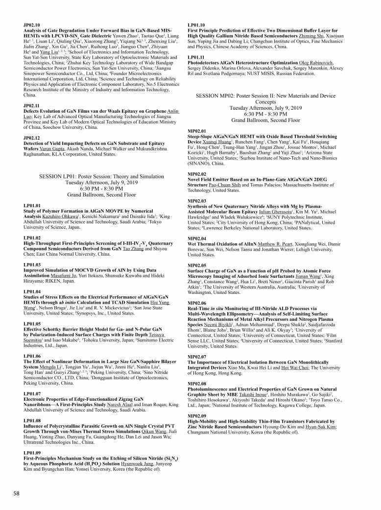
58
JP02.10 Analysis of Gate Degradation Under Forward Bias in GaN-Based MIS-HEMTs with LPCVD-SiNx Gate Dielectric Yawen Zhao1, Taotao Que1, Liang He1, 3, Liuan Li1, Qiuling Qiu1, Xiaorong Zhang3, Yiqiang Ni1, 3, Zhenxing Liu1, Jialin Zhang1, Xin Gu1, Jia Chen1, Ruihong Luo3, Jianguo Chen4, Zhiyuan He5 and Yang Liu1, 2, 3; 1School of Electronics and Information Technology, Sun Yat-Sen University, State Key Laboratory of Optoelectronic Materials and Technologies, China; 2Zhuhai Key Technology Laboratory of Wide Bandgap Semiconductor Power Electronics, Sun Yat-Sen University, China; 3Jiangsu Sinopower Semiconductor Co., Ltd, China; 4Founder Microelectronics International Corporation, Ltd, China; 5Science and Technology on Reliability Physics and Application of Electronic Component Laboratory, No.5 Electronics Research Institute of the Ministry of Industry and Information Technology, China.
JP02.11 Defects Evolution of GaN Films van der Waals Epitaxy on Graphene Anlin Luo; Key Lab of Advanced Optical Manufacturing Technologies of Jiangsu Province and Key Lab of Modern Optical Technologies of Education Ministry of China, Soochow University, China.
JP02.12 Detection of Yield Impacting Defects on GaN Substrate and Epitaxy Wafers Varun Gupta, Akash Nanda, Michael Walker and Mukundkrishna Raghunathan; KLA Corporation, United States.
SESSION LP01: Poster Session: Theory and Simulation Tuesday Afternoon, July 9, 2019
6:30 PM - 8:30 PM Grand Ballroom, Second Floor
LP01.01 Study of Polymer Formation in AlGaN MOVPE by Numerical Analysis Kazuhiro Ohkawa1, Kenichi Nakamura2 and Daisuke Iida1; 1King Abdullah University of Science and Technology, Saudi Arabia; 2Tokyo University of Science, Japan.
LP01.02 High-Throughput First-Principles Screening of I-III-IV2-V4 Quaternary Compound Semiconductors Derived from GaN Tao Zhang and Shiyou Chen; East China Normal University, China.
LP01.03 Improved Simulation of MOCVD Growth of AlN by Using Data Assimilation Masafumi Jo, Yuri Itokazu, Shunsuke Kuwaba and Hideki Hirayama; RIKEN, Japan.
LP01.04 Studies of Stress Effects on the Electrical Performance of AlGaN/GaN HEMTs through ab initio Calculation and TCAD Simulation Hiu Yung Wong1, Nelson Braga2, Jie Liu2 and R. V. Mickevicius2; 1San Jose State University, United States; 2Synopsys, Inc., United States.
LP01.05 Effective Schottky Barrier Height Model for Ga- and N-Polar GaN by Polarization-Induced Surface Charges with Finite Depth Tetsuya Suemitsu1 and Isao Makabe2; 1Tohoku University, Japan; 2Sumitomo Electric Industries, Ltd., Japan.
LP01.06 The Effect of Nonlinear Deformation in Large Size GaN/Sapphire Bilayer System Mengda Li1, Tongjun Yu1, Jiejun Wu1, Jinmi He2, Nanliu Liu3, Tong Han1 and Guoyi Zhang1, 2, 3; 1Peking University, China; 2Sino Nitride Semiconductor CO., LTD, China; 3Dongguan Institute of Optoelectronics, Peking University, China.
LP01.07 Electronic Properties of Edge-Functionalized Zigzag GaN Nanoribbons—A First-Principles Study Naresh Alaal and Iman Roqan; King Abdullah University of Science and Technology, Saudi Arabia.
LP01.08 Influence of Polycrystalline Parasitic Growth on AlN Single Crystal PVT Growth Through von-Mises Thermal Stress Simulations Qikun Wang, Jiali Huang, Yinting Zhao, Danyang Fu, Guangdong He, Dan Lei and Jason Wu; Ultratrend Technologies Inc., China.
LP01.09 First-Principles Mechanism Study on the Etching of Silicon Nitride (Si3N4) by Aqueous Phosphoric Acid (H3PO4) Solution Hyunwook Jung, Junyeop Kim and Byungchan Han; Yonsei University, Korea (the Republic of).
LP01.10 First Principle Prediction of Effective Two Dimensional Buffer Layer for High Quality Gallium Nitride Based Semiconductors Zhiming Shi, Xiaojuan Sun, Yuping Jia and Dabing Li; Changchun Institute of Optics, Fine Mechanics and Physics, Chinese Academy of Sciences, China.
LP01.11 Photodetectors AlGaN Heterostructure Optimization Oleg Rabinovich, Sergey Didenko, Marina Orlova, Alexander Savchuk, Sergey Marenkin, Alexey Ril and Svetlana Podgornaya; NUST MISIS, Russian Federation.
SESSION MP02: Poster Session II: New Materials and Device Concepts
Tuesday Afternoon, July 9, 2019 6:30 PM - 8:30 PM
Grand Ballroom, Second Floor
MP02.01 Steep-Slope AlGaN/GaN HEMT with Oxide Based Threshold Switching Device Xuanqi Huang1, Runchen Fang1, Chen Yang1, Kai Fu1, Houqiang Fu1, Hong Chen1, Tsung-Han Yang1, Jingan Zhou1, Jossue Montes1, Michael Kozicki1, Hugh Barnaby1, Baoshun Zhang2 and Yuji Zhao1; 1Arizona State University, United States; 2Suzhou Institute of Nano-Tech and Nano-Bionics (SINANO), China.
MP02.02 Novel Field Emitter Based on an In-Plane-Gate AlGaN/GaN 2DEG Structure Pao-Chuan Shih and Tomas Palacios; Massachusetts Institute of Technology, United States.
MP02.03 Synthesis of New Quaternary Nitride Alloys with Mg by Plasma-Assisted Molecular Beam Epitaxy Iulian Gherasoiu1, Kin M. Yu2, Michael Hawkridge3 and Wladek Walukiewicz4; 1SUNY Polytechnic Institute, United States; 2City University of Hong Kong, China; 3PANalytical, United States; 4Lawrence Berkeley National Laboratory, United States.
MP02.04 Wet Thermal Oxidation of AlInN Matthew R. Peart, Xiongliang Wei, Damir Borovac, Sun Wei, Nelson Tansu and Jonathan Wierer; Lehigh University, United States.
MP02.05 Surface Charge of GaN as a Function of pH Probed by Atomic Force Microscopy Imaging of Adsorbed Ionic Surfactants Jianan Wang1, Xing Zhang1, Constance Wang2, Hua Li1, Brett Nener1, Giacinta Parish1 and Rob Atkin1; 1The University of Western Australia, Australia; 2University of Washington, United States.
MP02.06 Real-Time in situ Monitoring of III-Nitride ALD Processes via Multi-Wavelength Ellipsometry—Analysis of Self-Limiting Surface Reaction Mechanisms of Metal Alkyl Precursors and Nitrogen Plasma Species Necmi Biyikli1, Adnan Mohammad1, Deepa Shukla2, Saidjafarzoda Ilhom1, Blaine Johs3, Brian Willis4 and Ali K. Okyay5; 1University of Connecticut, United States; 2University of Connecticut, United States; 3Film Sense LLC, United States; 4University of Connecticut, United States; 5Stanford University, United States.
MP02.07 The Importance of Electrical Isolation Between GaN Monolithically Integrated Devices Xiao Ma, Kwai Hei Li and Hoi Wai Choi; The University of Hong Kong, Hong Kong.
MP02.08 Photoluminescence and Electrical Properties of GaN Grown on Natural Graphite Sheet by MBE Takashi Inoue1, Hoshito Murakawa2, Go Sajiki2, Toshihiro Hosokawa1, Akiyoshi Takeda1 and Hiroshi Okano2; 1Toyo Tanso Co., Ltd., Japan; 2National Institute of Technology, Kagawa College, Japan.
MP02.09 High-Mobility and High-Stability Thin-Film Transistors Fabricated by Zinc Nitride Based Semiconductors Hyoung-Do Kim and Hyun-Suk Kim; Chungnam National University, Korea (the Republic of).
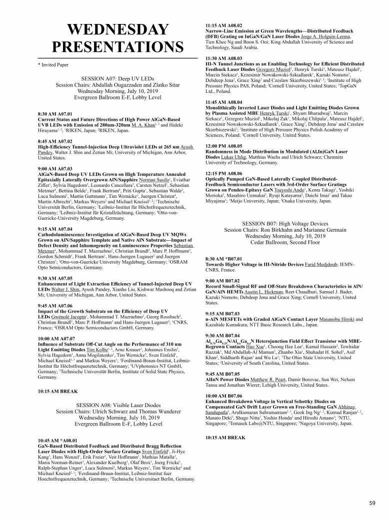
59
WEDNESDAY PRESENTATIONS
* Invited Paper
SESSION A07: Deep UV LEDs Session Chairs: Abdallah Ougazzaden and Zlatko Sitar
Wednesday Morning, July 10, 2019 Evergreen Ballroom E-F, Lobby Level
8:30 AM A07.01 Current Status and Future Directions of High Power AlGaN-Based UVB LEDs with Emission of 280nm-320nm M. A. Khan1, 2 and Hideki Hirayama1, 2; 1RIKEN, Japan; 2RIKEN, Japan.
8:45 AM A07.02 High-Efficiency Tunnel-Injection Deep Ultraviolet LEDs at 265 nm Ayush Pandey, Walter J. Shin and Zetian Mi; University of Michigan, Ann Arbor, United States.
9:00 AM A07.03 AlGaN-Based Deep UV LEDs Grown on High Temperature Annealed Epitaxially Laterally Overgrown AlN/Sapphire Norman Susilo1, Eviathar Ziffer1, Sylvia Hagedorn2, Leonardo Cancellara3, Carsten Netzel2, Sebastian Metzner4, Bettina Belde1, Frank Bertram4, Priti Gupta1, Sebastian Walde2, Luca Sulmoni1, Martin Guttmann1, Tim Wernicke1, Juergen Christen4, Martin Albrecht3, Markus Weyers2 and Michael Kneissl1, 2; 1Technische Universität Berlin, Germany; 2Leibniz-Institut für Höchstfrequenztechnik, Germany; 3Leibniz-Institut für Kristallzüchtung, Germany; 4Otto-von-Guericke-University Magdeburg, Germany.
9:15 AM A07.04 Cathodoluminescence Investigation of AlGaN-Based Deep UV MQWs Grown on AlN/Sapphire Template and Native AlN Substrate—Impact of Defect Density and Inhomogeneity on Luminescence Properties Sebastian Metzner1, Mohammad T. Mazraehno2, Christian Brandl2, Marc P. Hoffmann2, Gordon Schmidt1, Frank Bertram1, Hans-Juergen Lugauer2 and Juergen Christen1; 1Otto-von-Guericke University Magdeburg, Germany; 2OSRAM Opto Semiconductors, Germany.
9:30 AM A07.05 Enhancement of Light Extraction Efficiency of Tunnel-Injected Deep UV LEDs Walter J. Shin, Ayush Pandey, Xianhe Liu, Kishwar Mashooq and Zetian Mi; University of Michigan, Ann Arbor, United States.
9:45 AM A07.06 Impact of the Growth Substrate on the Efficiency of Deep UV LEDs Gwénolé Jacopin1, Mohammad T. Mazraehno2, Georg Rossbach2, Christian Brandl2, Marc P. Hoffmann2 and Hans-Juergen Lugauer2; 1CNRS, France; 2OSRAM Opto Semiconductors GmbH, Germany.
10:00 AM A07.07 Influence of Substrate Off-Cut Angle on the Performance of 310 nm Light Emitting Diodes Tim Kolbe1, 2, Arne Knauer1, Johannes Enslin3, Sylvia Hagedorn1, Anna Mogilatenko1, Tim Wernicke3, Sven Einfeld1, Michael Kneissl1, 3 and Markus Weyers1; 1Ferdinand-Braun-Institut, Leibniz-Institut für Höchstfrequenztechnik, Germany; 2UVphotonics NT GmbH, Germany; 3Technische Universität Berlin, Institute of Solid State Physics, Germany.
10:15 AM BREAK
SESSION A08: Visible Laser Diodes Session Chairs: Ulrich Schwarz and Thomas Wunderer
Wednesday Morning, July 10, 2019 Evergreen Ballroom E-F, Lobby Level
10:45 AM *A08.01 GaN-Based Distributed Feedback and Distributed Bragg Reflection Laser Diodes with High-Order Surface Gratings Sven Einfeld1, Ji-Hye Kang1, Hans Wenzel1, Erik Freier1, Veit Hoffmann1, Mathias Matalla1, Maria Norman-Reiner1, Alexander Kuelberg1, Olaf Brox1, Joerg Fricke1, Ralph-Stephan Unger1, Luca Sulmoni2, Markus Weyers1, Tim Wernicke2 and Michael Kneissl2, 1; 1Ferdinand-Braun-Institut, Leibniz-Institut fuer Hoechstfrequenztechnik, Germany; 2Technische Universitaet Berlin, Germany.
11:15 AM A08.02 Narrow-Line Emission at Green Wavelengths—Distributed Feedback (DFB) Grating on InGaN/GaN Laser Diodes Jorge A. Holguin-Lerma, Tien Khee Ng and Boon S. Ooi; King Abdullah University of Science and Technology, Saudi Arabia.
11:30 AM A08.03 III-N Tunnel Junctions as an Enabling Technology for Efficient Distributed Feedback Laser Diodes Grzegorz Muziol1, Henryk Turski1, Mateusz Hajdel1, Marcin Siekacz1, Krzesimir Nowakowski-Szkudlarek1, Kazuki Nomoto2, Debdeep Jena2, Grace Xing2 and Czeslaw Skierbiszewski1, 3; 1Institute of High Pressure Physics PAS, Poland; 2Cornell University, United States; 3TopGaN Ltd., Poland.
11:45 AM A08.04 Monolithically Inverted Laser Diodes and Light Emitting Diodes Grown by Plasma Assisted MBE Henryk Turski1, Shyam Bharadwaj2, Marcin Siekacz1, Grzegorz Muziol1, Mikolaj Zak1, Mikolaj Chlipala1, Mateusz Hajdel1, Krzesimir Nowakowski-Szkudlarek1, Grace Xing2, Debdeep Jena2 and Czeslaw Skierbiszewski1; 1Institute of High Pressure Physics Polish Academy of Sciences, Poland; 2Cornell University, United States.
12:00 PM A08.05 Randomness in Mode Distribution in Modulated (Al,In)GaN Laser Diodes Lukas Uhlig, Matthias Wachs and Ulrich Schwarz; Chemnitz University of Technology, Germany.
12:15 PM A08.06 Optically Pumped GaN-Based Laterally Coupled Distributed-Feedback Semiconductor Lasers with 3rd-Order Surface Gratings Grown on Pendeo-Epitaxy GaN Tsuyoshi Ando1, Kenta Takagi1, Yoshiki Morioka2, Masahiro Uemukai2, Ryuji Katayama2, Daichi Imai1 and Takao Miyajima1; 1Meijo University, Japan; 2Osaka University, Japan.
SESSION B07: High Voltage Devices Session Chairs: Ron Birkhahn and Marianne Germain
Wednesday Morning, July 10, 2019 Cedar Ballroom, Second Floor
8:30 AM *B07.01 Towards Higher Voltage in III-Nitride Devices Farid Medjdoub; IEMN-CNRS, France.
9:00 AM B07.02 Record Small-Signal RF and Off-State Breakdown Characteristics in AlN/GaN/AlN HEMTs Austin L. Hickman, Reet Chaudhuri, Samuel J. Bader, Kazuki Nomoto, Debdeep Jena and Grace Xing; Cornell University, United States.
9:15 AM B07.03 n-AlN MESFETs with Graded AlGaN Contact Layer Masanobu Hiroki and Kazuhide Kumakura; NTT Basic Research Labs., Japan.
9:30 AM B07.04 Al0.75Ga0.25N/Al0.6Ga0.4N Heterojunction Field Effect Transistor with MBE-Regrown Contacts Hao Xue1, Choong Hee Lee1, Kamal Hussain2, Towhidur Razzak1, Md Abdullah-Al Mamun2, Zhanbo Xia1, Shahadat H. Sohel1, Asif Khan2, Siddharth Rajan1 and Wu Lu1; 1The Ohio State University, United States; 2University of South Carolina, United States.
9:45 AM B07.05 AlInN Power Diodes Matthew R. Peart, Damir Borovac, Sun Wei, Nelson Tansu and Jonathan Wierer; Lehigh University, United States.
10:00 AM B07.06 Enhanced Breakdown Voltage in Vertical Schottky Diodes on Compensated GaN Drift Layer Grown on Free-Standing GaN Abhinay Sandupatla1, Arulkumaran Subramaniam2, 3, Geok Ing Ng1, 2, Kumud Ranjan1, 2, Manato Deki3, Shugo Nitta3, Yoshio Honda3 and Hiroshi Amano3; 1NTU, Singapore; 2Temasek Labs@NTU, Singapore; 3Nagoya University, Japan.
10:15 AM BREAK
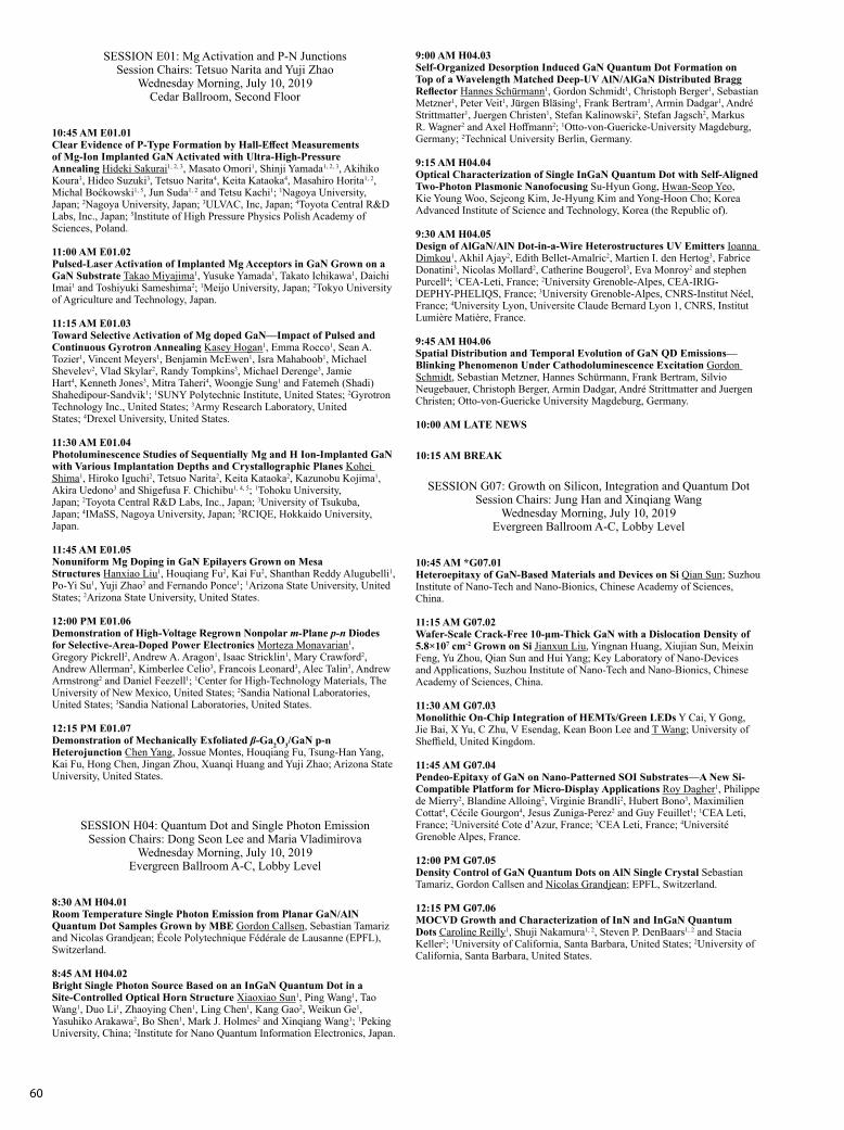
60
SESSION E01: Mg Activation and P-N Junctions Session Chairs: Tetsuo Narita and Yuji Zhao
Wednesday Morning, July 10, 2019 Cedar Ballroom, Second Floor
10:45 AM E01.01 Clear Evidence of P-Type Formation by Hall-Effect Measurements of Mg-Ion Implanted GaN Activated with Ultra-High-Pressure Annealing Hideki Sakurai1, 2, 3, Masato Omori1, Shinji Yamada1, 2, 3, Akihiko Koura3, Hideo Suzuki3, Tetsuo Narita4, Keita Kataoka4, Masahiro Horita1, 2, Michal Boćkowski1, 5, Jun Suda1, 2 and Tetsu Kachi1; 1Nagoya University, Japan; 2Nagoya University, Japan; 3ULVAC, Inc, Japan; 4Toyota Central R&D Labs, Inc., Japan; 5Institute of High Pressure Physics Polish Academy of Sciences, Poland.
11:00 AM E01.02 Pulsed-Laser Activation of Implanted Mg Acceptors in GaN Grown on a GaN Substrate Takao Miyajima1, Yusuke Yamada1, Takato Ichikawa1, Daichi Imai1 and Toshiyuki Sameshima2; 1Meijo University, Japan; 2Tokyo University of Agriculture and Technology, Japan.
11:15 AM E01.03 Toward Selective Activation of Mg doped GaN—Impact of Pulsed and Continuous Gyrotron Annealing Kasey Hogan1, Emma Rocco1, Sean A. Tozier1, Vincent Meyers1, Benjamin McEwen1, Isra Mahaboob1, Michael Shevelev2, Vlad Skylar2, Randy Tompkins3, Michael Derenge3, Jamie Hart4, Kenneth Jones3, Mitra Taheri4, Woongje Sung1 and Fatemeh (Shadi) Shahedipour-Sandvik1; 1SUNY Polytechnic Institute, United States; 2Gyrotron Technology Inc., United States; 3Army Research Laboratory, United States; 4Drexel University, United States.
11:30 AM E01.04 Photoluminescence Studies of Sequentially Mg and H Ion-Implanted GaN with Various Implantation Depths and Crystallographic Planes Kohei Shima1, Hiroko Iguchi2, Tetsuo Narita2, Keita Kataoka2, Kazunobu Kojima1, Akira Uedono3 and Shigefusa F. Chichibu1, 4, 5; 1Tohoku University, Japan; 2Toyota Central R&D Labs, Inc., Japan; 3University of Tsukuba, Japan; 4IMaSS, Nagoya University, Japan; 5RCIQE, Hokkaido University, Japan.
11:45 AM E01.05 Nonuniform Mg Doping in GaN Epilayers Grown on Mesa Structures Hanxiao Liu1, Houqiang Fu2, Kai Fu2, Shanthan Reddy Alugubelli1, Po-Yi Su1, Yuji Zhao2 and Fernando Ponce1; 1Arizona State University, United States; 2Arizona State University, United States.
12:00 PM E01.06 Demonstration of High-Voltage Regrown Nonpolar m-Plane p-n Diodes for Selective-Area-Doped Power Electronics Morteza Monavarian1, Gregory Pickrell2, Andrew A. Aragon1, Isaac Stricklin1, Mary Crawford2, Andrew Allerman2, Kimberlee Celio3, Francois Leonard3, Alec Talin3, Andrew Armstrong2 and Daniel Feezell1; 1Center for High-Technology Materials, The University of New Mexico, United States; 2Sandia National Laboratories, United States; 3Sandia National Laboratories, United States.
12:15 PM E01.07 Demonstration of Mechanically Exfoliated β-Ga2O3/GaN p-n Heterojunction Chen Yang, Jossue Montes, Houqiang Fu, Tsung-Han Yang, Kai Fu, Hong Chen, Jingan Zhou, Xuanqi Huang and Yuji Zhao; Arizona State University, United States.
SESSION H04: Quantum Dot and Single Photon Emission Session Chairs: Dong Seon Lee and Maria Vladimirova
Wednesday Morning, July 10, 2019 Evergreen Ballroom A-C, Lobby Level
8:30 AM H04.01 Room Temperature Single Photon Emission from Planar GaN/AlN Quantum Dot Samples Grown by MBE Gordon Callsen, Sebastian Tamariz and Nicolas Grandjean; École Polytechnique Fédérale de Lausanne (EPFL), Switzerland.
8:45 AM H04.02 Bright Single Photon Source Based on an InGaN Quantum Dot in a Site-Controlled Optical Horn Structure Xiaoxiao Sun1, Ping Wang1, Tao Wang1, Duo Li1, Zhaoying Chen1, Ling Chen1, Kang Gao2, Weikun Ge1, Yasuhiko Arakawa2, Bo Shen1, Mark J. Holmes2 and Xinqiang Wang1; 1Peking University, China; 2Institute for Nano Quantum Information Electronics, Japan.
9:00 AM H04.03 Self-Organized Desorption Induced GaN Quantum Dot Formation on Top of a Wavelength Matched Deep-UV AlN/AlGaN Distributed Bragg Reflector Hannes Schürmann1, Gordon Schmidt1, Christoph Berger1, Sebastian Metzner1, Peter Veit1, Jürgen Bläsing1, Frank Bertram1, Armin Dadgar1, André Strittmatter1, Juergen Christen1, Stefan Kalinowski2, Stefan Jagsch2, Markus R. Wagner2 and Axel Hoffmann2; 1Otto-von-Guericke-University Magdeburg, Germany; 2Technical University Berlin, Germany.
9:15 AM H04.04 Optical Characterization of Single InGaN Quantum Dot with Self-Aligned Two-Photon Plasmonic Nanofocusing Su-Hyun Gong, Hwan-Seop Yeo, Kie Young Woo, Sejeong Kim, Je-Hyung Kim and Yong-Hoon Cho; Korea Advanced Institute of Science and Technology, Korea (the Republic of).
9:30 AM H04.05 Design of AlGaN/AlN Dot-in-a-Wire Heterostructures UV Emitters Ioanna Dimkou1, Akhil Ajay2, Edith Bellet-Amalric2, Martien I. den Hertog3, Fabrice Donatini3, Nicolas Mollard2, Catherine Bougerol3, Eva Monroy2 and stephen Purcell4; 1CEA-Leti, France; 2University Grenoble-Alpes, CEA-IRIG-DEPHY-PHELIQS, France; 3University Grenoble-Alpes, CNRS-Institut Néel, France; 4University Lyon, Universite Claude Bernard Lyon 1, CNRS, Institut Lumière Matière, France.
9:45 AM H04.06 Spatial Distribution and Temporal Evolution of GaN QD Emissions—Blinking Phenomenon Under Cathodoluminescence Excitation Gordon Schmidt, Sebastian Metzner, Hannes Schürmann, Frank Bertram, Silvio Neugebauer, Christoph Berger, Armin Dadgar, André Strittmatter and Juergen Christen; Otto-von-Guericke University Magdeburg, Germany.
10:00 AM LATE NEWS
10:15 AM BREAK
SESSION G07: Growth on Silicon, Integration and Quantum Dot Session Chairs: Jung Han and Xinqiang Wang
Wednesday Morning, July 10, 2019 Evergreen Ballroom A-C, Lobby Level
10:45 AM *G07.01 Heteroepitaxy of GaN-Based Materials and Devices on Si Qian Sun; Suzhou Institute of Nano-Tech and Nano-Bionics, Chinese Academy of Sciences, China.
11:15 AM G07.02 Wafer-Scale Crack-Free 10-μm-Thick GaN with a Dislocation Density of 5.8×107 cm-2 Grown on Si Jianxun Liu, Yingnan Huang, Xiujian Sun, Meixin Feng, Yu Zhou, Qian Sun and Hui Yang; Key Laboratory of Nano-Devices and Applications, Suzhou Institute of Nano-Tech and Nano-Bionics, Chinese Academy of Sciences, China.
11:30 AM G07.03 Monolithic On-Chip Integration of HEMTs/Green LEDs Y Cai, Y Gong, Jie Bai, X Yu, C Zhu, V Esendag, Kean Boon Lee and T Wang; University of Sheffield, United Kingdom.
11:45 AM G07.04 Pendeo-Epitaxy of GaN on Nano-Patterned SOI Substrates—A New Si-Compatible Platform for Micro-Display Applications Roy Dagher1, Philippe de Mierry2, Blandine Alloing2, Virginie Brandli2, Hubert Bono3, Maximilien Cottat4, Cécile Gourgon4, Jesus Zuniga-Perez2 and Guy Feuillet1; 1CEA Leti, France; 2Université Cote d’Azur, France; 3CEA Leti, France; 4Université Grenoble Alpes, France.
12:00 PM G07.05 Density Control of GaN Quantum Dots on AlN Single Crystal Sebastian Tamariz, Gordon Callsen and Nicolas Grandjean; EPFL, Switzerland.
12:15 PM G07.06 MOCVD Growth and Characterization of InN and InGaN Quantum Dots Caroline Reilly1, Shuji Nakamura1, 2, Steven P. DenBaars1, 2 and Stacia Keller2; 1University of California, Santa Barbara, United States; 2University of California, Santa Barbara, United States.
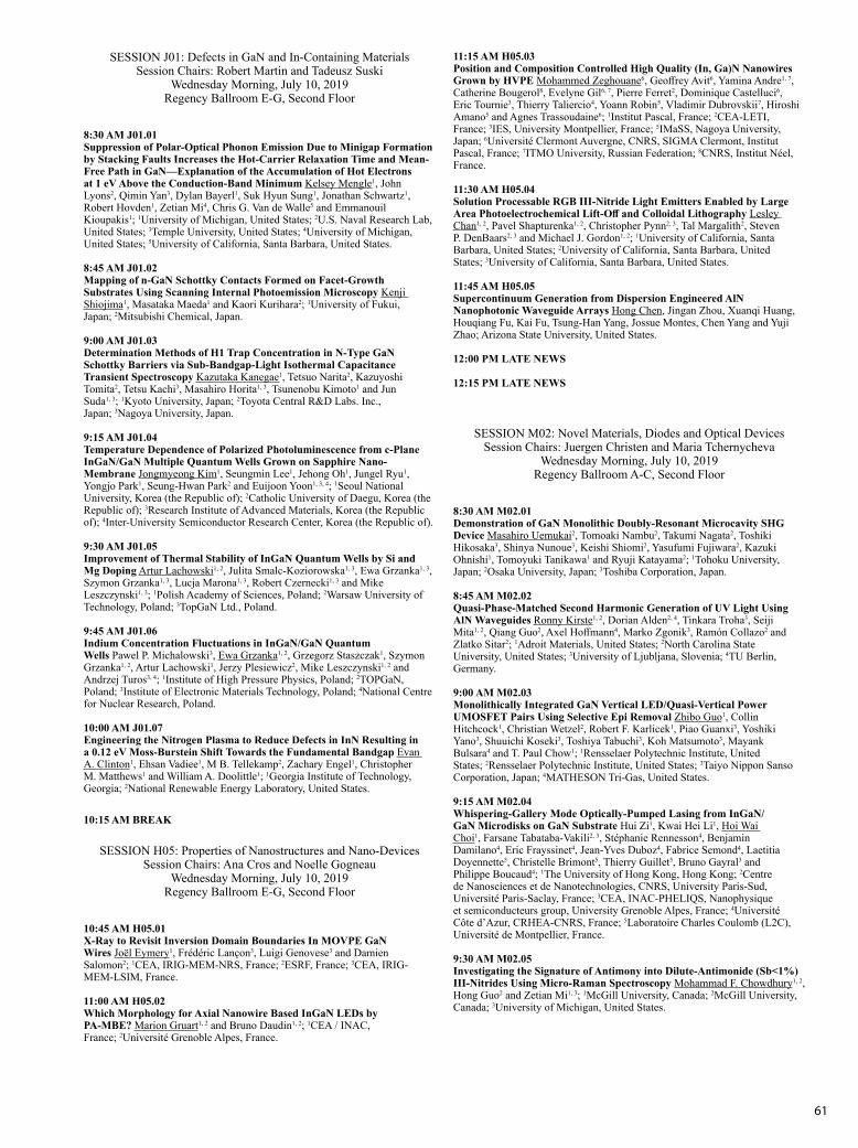
61
SESSION J01: Defects in GaN and In-Containing Materials Session Chairs: Robert Martin and Tadeusz Suski
Wednesday Morning, July 10, 2019 Regency Ballroom E-G, Second Floor
8:30 AM J01.01 Suppression of Polar-Optical Phonon Emission Due to Minigap Formation by Stacking Faults Increases the Hot-Carrier Relaxation Time and Mean-Free Path in GaN—Explanation of the Accumulation of Hot Electrons at 1 eV Above the Conduction-Band Minimum Kelsey Mengle1, John Lyons2, Qimin Yan3, Dylan Bayerl1, Suk Hyun Sung1, Jonathan Schwartz1, Robert Hovden1, Zetian Mi4, Chris G. Van de Walle5 and Emmanouil Kioupakis1; 1University of Michigan, United States; 2U.S. Naval Research Lab, United States; 3Temple University, United States; 4University of Michigan, United States; 5University of California, Santa Barbara, United States.
8:45 AM J01.02 Mapping of n-GaN Schottky Contacts Formed on Facet-Growth Substrates Using Scanning Internal Photoemission Microscopy Kenji Shiojima1, Masataka Maeda1 and Kaori Kurihara2; 1University of Fukui, Japan; 2Mitsubishi Chemical, Japan.
9:00 AM J01.03 Determination Methods of H1 Trap Concentration in N-Type GaN Schottky Barriers via Sub-Bandgap-Light Isothermal Capacitance Transient Spectroscopy Kazutaka Kanegae1, Tetsuo Narita2, Kazuyoshi Tomita2, Tetsu Kachi3, Masahiro Horita1, 3, Tsunenobu Kimoto1 and Jun Suda1, 3; 1Kyoto University, Japan; 2Toyota Central R&D Labs. Inc., Japan; 3Nagoya University, Japan.
9:15 AM J01.04 Temperature Dependence of Polarized Photoluminescence from c-Plane InGaN/GaN Multiple Quantum Wells Grown on Sapphire Nano-Membrane Jongmyeong Kim1, Seungmin Lee1, Jehong Oh1, Jungel Ryu1, Yongjo Park1, Seung-Hwan Park2 and Euijoon Yoon1, 3, 4; 1Seoul National University, Korea (the Republic of); 2Catholic University of Daegu, Korea (the Republic of); 3Research Institute of Advanced Materials, Korea (the Republic of); 4Inter-University Semiconductor Research Center, Korea (the Republic of).
9:30 AM J01.05 Improvement of Thermal Stability of InGaN Quantum Wells by Si and Mg Doping Artur Lachowski1, 2, Julita Smalc-Koziorowska1, 3, Ewa Grzanka1, 3, Szymon Grzanka1, 3, Lucja Marona1, 3, Robert Czernecki1, 3 and Mike Leszczynski1, 3; 1Polish Academy of Sciences, Poland; 2Warsaw University of Technology, Poland; 3TopGaN Ltd., Poland.
9:45 AM J01.06 Indium Concentration Fluctuations in InGaN/GaN Quantum Wells Pawel P. Michalowski3, Ewa Grzanka1, 2, Grzegorz Staszczak1, Szymon Grzanka1, 2, Artur Lachowski1, Jerzy Plesiewicz2, Mike Leszczynski1, 2 and Andrzej Turos3, 4; 1Institute of High Pressure Physics, Poland; 2TOPGaN, Poland; 3Institute of Electronic Materials Technology, Poland; 4National Centre for Nuclear Research, Poland.
10:00 AM J01.07 Engineering the Nitrogen Plasma to Reduce Defects in InN Resulting in a 0.12 eV Moss-Burstein Shift Towards the Fundamental Bandgap Evan A. Clinton1, Ehsan Vadiee1, M B. Tellekamp2, Zachary Engel1, Christopher M. Matthews1 and William A. Doolittle1; 1Georgia Institute of Technology, Georgia; 2National Renewable Energy Laboratory, United States.
10:15 AM BREAK
SESSION H05: Properties of Nanostructures and Nano-Devices Session Chairs: Ana Cros and Noelle Gogneau
Wednesday Morning, July 10, 2019 Regency Ballroom E-G, Second Floor
10:45 AM H05.01 X-Ray to Revisit Inversion Domain Boundaries In MOVPE GaN Wires Joël Eymery1, Frédéric Lançon3, Luigi Genovese3 and Damien Salomon2; 1CEA, IRIG-MEM-NRS, France; 2ESRF, France; 3CEA, IRIG-MEM-LSIM, France.
11:00 AM H05.02 Which Morphology for Axial Nanowire Based InGaN LEDs by PA-MBE? Marion Gruart1, 2 and Bruno Daudin1, 2; 1CEA / INAC, France; 2Université Grenoble Alpes, France.
11:15 AM H05.03 Position and Composition Controlled High Quality (In, Ga)N Nanowires Grown by HVPE Mohammed Zeghouane6, Geoffrey Avit6, Yamina Andre1, 7, Catherine Bougerol8, Evelyne Gil6, 7, Pierre Ferret2, Dominique Castelluci6, Eric Tournie3, Thierry Taliercio4, Yoann Robin5, Vladimir Dubrovskii7, Hiroshi Amano5 and Agnes Trassoudaine6; 1Institut Pascal, France; 2CEA-LETI, France; 3IES, University Montpellier, France; 5IMaSS, Nagoya University, Japan; 6Université Clermont Auvergne, CNRS, SIGMA Clermont, Institut Pascal, France; 7ITMO University, Russian Federation; 8CNRS, Institut Néel, France.
11:30 AM H05.04 Solution Processable RGB III-Nitride Light Emitters Enabled by Large Area Photoelectrochemical Lift-Off and Colloidal Lithography Lesley Chan1, 2, Pavel Shapturenka1, 2, Christopher Pynn2, 3, Tal Margalith2, Steven P. DenBaars2, 3 and Michael J. Gordon1, 2; 1University of California, Santa Barbara, United States; 2University of California, Santa Barbara, United States; 3University of California, Santa Barbara, United States.
11:45 AM H05.05 Supercontinuum Generation from Dispersion Engineered AlN Nanophotonic Waveguide Arrays Hong Chen, Jingan Zhou, Xuanqi Huang, Houqiang Fu, Kai Fu, Tsung-Han Yang, Jossue Montes, Chen Yang and Yuji Zhao; Arizona State University, United States.
12:00 PM LATE NEWS
12:15 PM LATE NEWS
SESSION M02: Novel Materials, Diodes and Optical Devices Session Chairs: Juergen Christen and Maria Tchernycheva
Wednesday Morning, July 10, 2019 Regency Ballroom A-C, Second Floor
8:30 AM M02.01 Demonstration of GaN Monolithic Doubly-Resonant Microcavity SHG Device Masahiro Uemukai2, Tomoaki Nambu2, Takumi Nagata2, Toshiki Hikosaka3, Shinya Nunoue3, Keishi Shiomi2, Yasufumi Fujiwara2, Kazuki Ohnishi1, Tomoyuki Tanikawa1 and Ryuji Katayama2; 1Tohoku University, Japan; 2Osaka University, Japan; 3Toshiba Corporation, Japan.
8:45 AM M02.02 Quasi-Phase-Matched Second Harmonic Generation of UV Light Using AlN Waveguides Ronny Kirste1, 2, Dorian Alden2, 4, Tinkara Troha3, Seiji Mita1, 2, Qiang Guo2, Axel Hoffmann4, Marko Zgonik3, Ramón Collazo2 and Zlatko Sitar2; 1Adroit Materials, United States; 2North Carolina State University, United States; 3University of Ljubljana, Slovenia; 4TU Berlin, Germany.
9:00 AM M02.03 Monolithically Integrated GaN Vertical LED/Quasi-Vertical Power UMOSFET Pairs Using Selective Epi Removal Zhibo Guo1, Collin Hitchcock1, Christian Wetzel2, Robert F. Karlicek1, Piao Guanxi3, Yoshiki Yano3, Shuuichi Koseki3, Toshiya Tabuchi3, Koh Matsumoto3, Mayank Bulsara4 and T. Paul Chow1; 1Rensselaer Polytechnic Institute, United States; 2Rensselaer Polytechnic Institute, United States; 3Taiyo Nippon Sanso Corporation, Japan; 4MATHESON Tri-Gas, United States.
9:15 AM M02.04 Whispering-Gallery Mode Optically-Pumped Lasing from InGaN/GaN Microdisks on GaN Substrate Hui Zi1, Kwai Hei Li1, Hoi Wai Choi1, Farsane Tabataba-Vakili2, 3, Stéphanie Rennesson4, Benjamin Damilano4, Eric Frayssinet4, Jean-Yves Duboz4, Fabrice Semond4, Laetitia Doyennette5, Christelle Brimont5, Thierry Guillet5, Bruno Gayral3 and Philippe Boucaud4; 1The University of Hong Kong, Hong Kong; 2Centre de Nanosciences et de Nanotechnologies, CNRS, University Paris-Sud, Université Paris-Saclay, France; 3CEA, INAC-PHELIQS, Nanophysique et semiconducteurs group, University Grenoble Alpes, France; 4Université Côte d’Azur, CRHEA-CNRS, France; 5Laboratoire Charles Coulomb (L2C), Université de Montpellier, France.
9:30 AM M02.05 Investigating the Signature of Antimony into Dilute-Antimonide (Sb<1%) III-Nitrides Using Micro-Raman Spectroscopy Mohammad F. Chowdhury1, 2, Hong Guo2 and Zetian Mi1, 3; 1McGill University, Canada; 2McGill University, Canada; 3University of Michigan, United States.
62
9:45 AM M02.06 First Demonstration of Negative Differential Resistance in AlxGa1-xN Homojunction Tunnel Diodes up to x=0.19 and High Reverse Bias Tunneling up to x=0.58 to Enable Ultraviolet Optoelectronics Evan A. Clinton, Ehsan Vadiee, Zachary Engel, Christopher M. Matthews and William A. Doolittle; Georgia Institute of Technology, Georgia.
10:00 AM M02.07 Epitaxial β-Ga2O3/Al0.45Ga0.55N Heterojunction-Based Schottky Barrier Diodes for Room and High Temperature Broadband Deep-Ultraviolet Optoelectronics Anisha Kalra, Shashwat Rathkanthiwar, Sandeep Vura, Rangarajan Muralidharan, Srinivasan Raghavan and Digbijoy N. Nath; Indian Institute of Science, India.
10:15 AM BREAK
SESSION M03: Transition Metal and Other Novel Nitrides Session Chairs: Kazuhiro Ohkawa and Stefan Schulz
Wednesday Morning, July 10, 2019 Regency Ballroom A-C, Second Floor
10:45 AM *M03.01 ScAlN-Based Ferroelectric and Piezoelectric Electro Acoustic Devices Oliver Ambacher1, 2, Agne Zukauskaite1, A. Ding1, Lutz Kirste1, N. Kurz2, N. Feil2, D. Urban3 and B. Heinz4; 1Fraunhofer Institute for Applied Solid State Physics, Germany; 2Institut for Sustainable Systems Engineering, Germany; 3Fraunhofer IWM, Germany; 4Evatec, Switzerland.
11:15 AM *M03.02 Epitaxial Transition-Metal Nitrides—ScAlN, NbNx, and TaNx for Next-Generation Electronic Devices Matthew T. Hardy, Scott Katzer, Brian P. Downey, Neeraj Nepal, Mario Ancona, Eric N. Jin, David Storm and David Meyer; Naval Research Laboratory, United States.
11:45 AM M03.03 Prediction and Synthesis of Mg-Sb-N Ternary Nitrides with Wurtzite-Derived and Antiperovskite Structures Karen Heinselman, Stephan Lany, John Perkins and Andriy Zakutayev; National Renewable Energy Laboratory, United States.
12:00 PM M03.04 A Map of New Ternary Metal Nitride Semiconductors Wenhao Sun; Lawrence Berkeley National Labs, United States.
12:15 PM M03.05 MOCVD Growth and Characterization of ZnGeN2-GaN Alloy Films Benthara H. Jayatunga1, Md Rezaul Karim2, Kathleen Kash1 and Hongping Zhao2; 1Case Western Reserve University, United States; 2Ohio State University, United States.
SESSION A09: Micro LEDs Session Chairs: Kate Kelchner and Jong Kyu Kim
Wednesday Afternoon, July 10, 2019 Evergreen Ballroom E-F, Lobby Level
2:00 PM *A09.01 Self-Passivated High-Efficiency c-Plane Micro-LED Array without Singulation Fabricated on Sapphire Nano-Membrane Structures Seungmin Lee1, Jongmyeong Kim1, Jehong Oh1, Jungel Ryu1, Yongjo Park1 and Euijoon Yoon2, 3, 4; 1Seoul National University, Korea (the Republic of); 3Research Institute of Advanced Materials, Seoul National University, Korea (the Republic of); 4Inter-University Semiconductor Research Center, Seoul National University, Korea (the Republic of).
2:30 PM A09.02 Efficient Green Semipolar (11-22) InGaN Micro-Light-Emitting Diodes on (11-22) GaN/Sapphire Template Matthew Wong1, Michel Khoury1, Hongjian Li1, Bastien Bonef1, Haojun Zhang2, Aidan A. Taylor1, Jared A. Kearns1, Philippe de Mierry3, James Speck1, Shuji Nakamura1, 2 and Steven P. DenBaars1, 2; 1University of California, Santa Barbara, United States; 2University of California, Santa Barbara, United States; 3CNRS-CRHEA, France.
2:45 PM A09.03 Near-Complete Elimination of Size-Dependent Efficiency Decrease of GaN Micro-LEDs by Using Neutral-Beam Etching Xuelun Wang1, 2, 3, Jun Zhu3, Tokio Takahashi3, Kazuhiko Endo4, Daisuke Ohori5 and Seiji Samukawa5, 6, 4; 1National Institute of Advanced Industrial Science and Technology, Japan; 2Nagoya University, Japan; 3National Institute of Advanced Industrial Science and Technology, Japan; 4National Institute of Advanced Industrial Science and Technology, Japan; 5Tohoku University, Japan; 6Tohoku University, Japan.
3:00 PM A09.04 Blue MicroLED Arrays on Flexible Metal Foils Abdelrahman T. Elshafiey1, Kenneth Davico1, Ashwin K. Rishinaramangalam1, Christopher Sheehan2, Vladimir Matias2 and Daniel Feezell1; 1University of New Mexico, United States; 2iBeam Materials, United States.
3:15 PM LATE NEWS
3:30 PM LATE NEWS
3:45 PM BREAK
SESSION A10: Intra Center, UV and BN Emitters Session Chairs: Nicolas Grandjean and Jennifer Hite
Wednesday Afternoon, July 10, 2019 Evergreen Ballroom E-F, Lobby Level
4:15 PM *A10.01 Development of Semiconductors Intra-Center Photonics Yasufumi Fujiwara, Keishi Shiomi, Yutaka Sasaki, Tomohiro Inaba, Shuhei Ichikawa and Jun Tatebayashi; Osaka University, Japan.
4:45 PM A10.02 Design of Composition-Graded p-AlGaN Cladding Layer for UVB Laser Diode Structure Kosuke Sato1, 2, Shinji Yasue2, Yuya Ogino2, Shunya Tanaka2, Motoaki Iwaya2, Tetsuya Takeuchi2, Satoshi Kamiyama2 and Isamu Akasaki2, 3; 1Asahi-Kasei, Japan; 2Meijo University, Japan; 3Nagoya University, Japan.
5:00 PM A10.03 Realization of High Light Output Power in AlGaN-Based UVB LED at 310±2nm Emission Using Highly Relaxed (50%) n-AlGaN Electron Injection Layer M. A. Khan1, 2, 3, Noritoshi Maeda1, Masafumi Jo1, Sachie Fujikawa1, 2, Eriko Matsuura1, 3, Yukio Kashima1, 3, Yoichi Yamada4 and Hideki Hirayama1; 1Riken, Japan, Japan; 2Tokyo Denki University, Japan; 3Marubun Corporation, Japan; 4Yamaguchi University, Japan.
5:15 PM A10.04 Boron Nitride Deep Ultraviolet Light Emitters Grown by Ultra-High-Temperature Molecular Beam Epitaxy David A. Laleyan1, Eric T. Reid1, Kelsey Mengle2, Emmanouil Kioupakis2 and Zetian Mi1; 1University of Michigan, United States; 2University of Michigan, United States.
5:30 PM A10.05 First Principles Calculations of Boron Alloyed Group III Nitrides for Higher Efficiency UV and Visible LEDs Logan D. Williams1, Kevin Greenman2 and Emmanouil Kioupakis1; 1University of Michigan, United States; 2University of Michigan, United States.
5:45 PM A10.06 Time-Resolved Luminescence Studies of Indirect Excitons in h-BN Epitaxial Films Grown by Chemical Vapor Deposition Using Carbon-Free Precursors Shigefusa F. Chichibu1, 2, 3, Naoki Umehara4, Keisuke Takiguchi5, Kohei Shima1, Kazunobu Kojima1, Yoshihiro Ishitani5 and Kazuhiko Hara4; 1Tohoku University, Japan; 2Nagoya University, Japan; 3Hokkaido University, Japan; 4Shizuoka University, Japan; 5Chiba University, Japan.
SESSION B08: MOS Transistors and Diodes Session Chairs: Martin Kuball and Matteo Meneghini
Wednesday Afternoon, July 10, 2019 Cedar Ballroom, Second Floor
2:00 PM *B08.01 Interface Control of Al2O3-Based MOS Structures for Advanced GaN Transistors Tamotsu Hashizume and Taketomo Sato; Hokkaido University, Japan.
63
2:30 PM B08.02 Gate-Channel Mobility Enhancement by Using AlN Interlayer in Recessed-Gate GaN-MOSFETs Akira Mukai, Daimotsu Kato, Yousuke Kajiwara, Hiroshi Ono, Aya Shindome and Masahiko Kuraguchi; Toshiba Corporation, Japan.
2:45 PM B08.03 Control of MOS Channel Characteristics of GaN-DIMOSFETs Formed by Mg Ion Implantation Ryo Tanaka1, Shinya Takashima1, Katsunori Ueno1, Hideaki Matsuyama1, Masaharu Edo1 and Kiyokazu Nakagawa2; 1Fuji Electric Co., Ltd., Japan; 2University of Yamanashi, Japan.
3:00 PM B08.04 Impact of Gamma-Ray Irradiation on Capacitance-Voltage Characteristics of Al2O3/GaN MOS Diodes with Post-Metallization Annealing Keito Aoshima1, Masahiro Horita1, 2, Shota Kaneki3, Jun Suda1, 2 and Tamotsu Hashizume3; 1Nagoya University, Japan; 2Nagoya University, Japan; 3Hokkaido University, Japan.
3:15 PM B08.05 Integrable Quasi-Vertical GaN UMOSFETs for Power and Optoelectronic ICs Zhibo Guo1, Collin Hitchcock1, Piao Guanxi2, Yoshiki Yano2, Shuuichi Koseki2, Toshiya Tabuchi2, Koh Matsumoto2, Mayank Bulsara3 and T. Paul Chow1; 1Rensselaer Polytechnic Institute, United States; 2Taiyo Nippon Sanso Corporation, Japan; 3MATHESON Tri-Gas, United States.
3:30 PM B08.06 Exploring the Electrical Properties of Gate Dielectrics on (000-1) N-Polar GaN Islam Sayed, Wenjian Liu, Silvia Chan, Chirag Gupta, Haoran Li, Matthew Guidry, Stacia Keller and Umesh K. Mishra; University of California, Santa Barbara, United States.
3:45 PM BREAK
SESSION B09: Electronic Device Characterization Session Chairs: Kei May Lau and Enrico Zanoni
Wednesday Afternoon, July 10, 2019 Cedar Ballroom, Second Floor
4:15 PM *B09.01 Impact of Deep Levels on GaN HEMTs Michael J. Uren and Martin Kuball; University of Bristol, United Kingdom.
4:45 PM B09.02 Dependence of the Current Collapse of GaN HEMTs on Quiescent Gate Voltage Takashi Matsuda1, Shigeo Yamabe2, Eiji Yagyu1 and Mikio Yamamuka1; 1Mitsubishi Electric Corporation, Japan; 2MELCO Semiconductor Engineering Corporation, Japan.
5:00 PM B09.03 Dopant Profiling in p-i-n GaN Structures Using Secondary Electrons Shanthan Reddy Alugubelli1, Hanxiao Liu1, Houqiang Fu2, Kai Fu2, Yuji Zhao2 and Fernando Ponce1; 1Arizona State University, United States; 2Arizona State University, United States.
5:15 PM B09.04 Impact of n-GaN Cap Layer on Gate Leakage Behavior in AlGaN/GaN Heterostructures Grown on Si and GaN Substrates Junji Kotani, Atsushi Yamada and Norikazu Nakamura; Fujitsu Limited, Japan.
5:30 PM B09.05 High Temperature Reverse Bias (HTRB) Tests on GaN Lateral HEMTs Xiang Zhou and T. Paul Chow; Rensselaer Polytechnic Institute (RPI), United States.
5:45 PM B09.06 Impact of Gamma-Ray Irradiation on Device Characteristics of p-GaN/AlGaN/GaN Normally-Off High-Electron-Mobility Transistors Koki Tsurimoto1, Masahiro Horita1, 2 and Jun Suda1, 2; 1Nagoya University, Japan; 2Nagoya University, Japan.
SESSION F03: Bulk and HVPE Growth Session Chairs: Rafael Dalmau and Yusuke Mori
Wednesday Afternoon, July 10, 2019 Regency Ballroom A-C, Second Floor
2:00 PM *F03.01 High Pressure in Physics and Technology of Bulk GaN Crystallization and Wafer Processing Izabella Grzegory; Institute of High Pressure Physics PAS Unipress, Poland.
2:30 PM F03.02 Crystallization of GaN by HVPE Method with Controlled Lateral Growth Tomasz Sochacki, Slawek Sakowski, Boleslaw Lucznik, Mikolaj Amilusik, Michal Fijalkowski, Malgorzata Iwinska, Aneta Sidor, Izabella Grzegory and Michal Boćkowski; Institute of High Pressure Physics PAS, Poland.
2:45 PM F03.03 HVPE-GaN Doped with Carbon and/or Manganese Malgorzata Iwinska, Tomasz Sochacki, Mikolaj Amilusik, Boleslaw Lucznik, Michal Fijalkowski, Marcin Zajac, Elzbieta Litwin-Staszewska, Ryszard Piotrzkowski, Leszek Konczewicz, Aneta Sidor, Kacper Sierakowski, Izabella Grzegory and Michal Boćkowski; Institute of High Pressure Physics Polish Academy of Sciences (Unipress), Poland.
3:00 PM F03.04 Growth of High Crystalline Quality GaN with High Growth Rate by THVPE Akira Yamaguchi1, Daisuke Oozeki2, Naoya Kawamoto2, Nao Takekawa2, Mayank Bulsara3, Hisashi Murakami2, Yoshinao Kumagai2, Koh Matsumoto1 and Akinori Koukitu2; 1Taiyo Nippon Sanso Co., Japan; 2Tokyo University of Agriculture and Technology, Japan; 3Matheson Tri-Gas, Inc., United States.
3:15 PM LATE NEWS
3:30 PM LATE NEWS
3:45 PM BREAK
SESSION A11: Efficiency and Degradation in Light Emitters Session Chairs: Aurelien David and Martin Strassburg
Wednesday Afternoon, July 10, 2019 Regency Ballroom A-C, Second Floor
4:15 PM A11.01 Physical Limits of Recombinations in III-Nitride LEDs Aurelien David, Nathan Young, Cory Lund and Michael Craven; Soraa, United States.
4:30 PM A11.02 Hot Carrier Generation—Without Efficiency Droop—In Low Radiative Efficiency MBE-Grown III-Nitride LEDs Andrew C. Espenlaub1, Daniel J. Myers1, Erin C. Young1, Saulius Marcinkevicius2, Claude Weisbuch1 and James Speck1; 1University of California, Santa Barbara, United States; 2KTH Royal Institute of Technology, Sweden.
4:45 PM A11.03 Photon-Driven Degradation Processes in GaN-Based Optoelectronic Devices Carlo De Santi1, Alessandro Caria1, Nicola Renso1, Ezgi Dogmus2, Malek Zegaoui2, Farid Medjdoub2, Gaudenzio Meneghesso1, Enrico Zanoni1 and Matteo Meneghini1; 1University of Padova, Italy; 2IEMN-CNRS, France.
5:00 PM A11.04 Effects of Well Width Fluctuations on Green InGaN/GaN Quantum Wells Grown at Different Temperatures Boning Ding, John Jarman, Menno Kappers and Rachel Oliver; University of Cambridge, United Kingdom.
5:15 PM A11.05 Contribution of Polarization-Induced Barriers to Excess Forward Voltage in c-Plane Green LEDs Cheyenne Lynsky1, Guillaume Lheureux1, Abdullah Alhassan1, Ryan White1, Bastien Bonef1, Yuh-Renn Wu2, Claude Weisbuch3, Steven P. DenBaars1, Shuji Nakamura1 and James Speck1; 1University of California, Santa Barbara, United States; 2National Taiwan University, Taiwan; 3Ecole Polytechnique, CNRS, Université Paris Saclay, France.
5:30 PM A11.06 Interwell Carrier Transport in InGaN/(In)GaN Multiple Quantum Wells Saulius Marcinkevicius1, Rinat Yapparov1, Leah Kuritzky2, Shuji Nakamura2, Steven P. DenBaars2 and James Speck2; 1KTH Royal Institute of Technology, Sweden; 2University of California, Santa Barbara, United States.
5:45 PM A11.07 Measurements of Internal Quantum Efficiency in Various InGaN Single Quantum Wells with Different Qualities by Simultaneous Photoacoustic and Photoluminescence Spectroscopy Keito Mori1, Yuchi Takahashi1, Atsushi A. Yamaguchi1, Yuya Kanitani2, Yoshihiro Kudo2 and Shigetaka Tomiya2; 1Kanazawa Institute of Technology, Japan; 2SONY Corporations, Japan.
64
SESSION G08: Growth for Electronic Devices including C-Doping Session Chairs: Koh Matsumoto and Yan Tang
Wednesday Afternoon, July 10, 2019 Evergreen Ballroom A-C, Lobby Level
2:00 PM G08.01 200 mm Industrial-Ready Dispersion-Free GaN-on-Si Buffer Technology for 650 V Rated Power Application Ming Zhao1, Xiangdong Li1, 2 and Stefaan Decoutere1; 1imec, Belgium; 2KU Leuven, Belgium.
2:15 PM G08.02 Extrinsic Carbon Doped AlGaN/AlN Super-Lattice Buffer for Power Electronic Applications Beyond 1000V Dirk Fahle, Matthias Marx, Hannes Behmenburg, Manuel Kortemeyer and Michael Heuken; AIXTRON SE, Germany.
2:30 PM G08.03 Understanding GaN Homoepitaxial Growth and Substrate-Dependent Effects for Vertical Power Devices Jennifer K. Hite, Travis J. Anderson, James C. Gallagher, Michael A. Mastro, Jaime Freitas, John Lyons, Karl Hobart, Charles R. Eddy Jr. and Francis J. Kub; U.S. Naval Research Laboratory, United States.
2:45 PM G08.04 GaN Micropillar Schottky Diodes with High Breakdown Field Strength Fabricated by Selective-Area Growth Arne Debald1, Simon Kotzea1, Michael Heuken1, 2, Holger Kalisch1 and Andrei Vescan1; 1RWTH Aachen, Germany, Germany; 2AIXTRON SE, Germany.
3:00 PM G08.05 Compensation in Semi-Insulating Free-Standing GaN:C Substrates—A Carbon-Related Defect Mary Ellen Zvanut1, Subash Paudel1, Malgorzata Iwinska2, Tomasz Sochacki2 and Michal Boćkowski2; 1University of Alabama at Birmingham, United States; 2Polish Academy of Sciences, Poland.
3:15 PM G08.06 Dependences of External Quantum Efficiency of Radiation and Photoluminescence Lifetime on the Carbon Concentration in GaN on GaN Structures Kazunobu Kojima1, Fumimasa Horikiri2, Yoshinobu Narita2, Takehiro Yoshida2 and Shigefusa F. Chichibu1; 1Tohoku University, Japan; 2Sciocs Co. Ltd., Japan.
3:30 PM G08.07 Eutectic Formation and Polarity Inversion in Nitrides on Silicon Alexana Roshko, Matt Brubaker, Paul Blanchard, Todd Harvey and Kris Bertness; National Institute of Standards and Technology, United States.
3:45 PM BREAK
SESSION G09: Growth Kinetic and Theory Session Chairs: James Speck and Euijoon Yoon
Wednesday Afternoon, July 10, 2019 Evergreen Ballroom A-C, Lobby Level
4:15 PM *G09.01 A New Theoretical Approach to Nitride Crystal Growth—Impurity Incorporation Mechanism Yoshihiro Kangawa1, 2, Pawel Kempisty3, 1, 2 and Kenji Shiraishi2; 1Kyushu University, Japan; 2Nagoya University, Japan; 3Polish Academy of Sciences, Poland.
4:45 PM G09.02 Equilibrium Morphologies of Faceted GaN under Metalorganic Vapor Phase Epitaxy Condition—Wulff Construction Using Absolute Surface Energies Yuki Seta, Abdul Pradipto, Toru Akiyama, Kohji Nakamura and Tomonori Ito; Mie University, Japan.
5:00 PM G09.03 Control of Growth Kinetics Towards Enhanced Red Emissions from Strongly Excited Eu-Doped GaN Shuhei Ichikawa, Jun Tatebayashi and Yasufumi Fujiwara; Osaka University, Japan.
5:15 PM G09.04 Surface Kinetics of GaN Homoepitaxial Growth via MOCVD Andrew Klump1, Pramod Reddy2, Yan Guan1, Shun Washiyama1, Seiji Mita2, Ramón Collazo1 and Zlatko Sitar1; 1North Carolina State University, United States; 2Adroit Materials, United States.
5:30 PM G09.05 Theoretical Study on Step Bunching Instability During Nitride Semiconductor Growth Yuya Inatomi1 and Yoshihiro Kangawa1, 2, 3; 1Kyushu University, Japan; 2RIAM, Kyushu University, Japan; 3IMaSS, Nagoya University, Japan.
5:45 PM G09.06 Shell Growth Mechanisms on GaN Fin Microstructures Irene Manglano Clavero1, 2, Christoph Margenfeld1, 2, Hergo-Heinrich Wehmann1, 2, Adrian Avramescu3, Hans-Juergen Lugauer3 and Andreas Waag1, 2; 1Technische Universität Braunschweig, Germany; 2Epitaxy Competence Center ec2, Germany; 3Osram Opto Semiconductors GmbH, Germany.
SESSION J02: Structural Defects in Electronic Devices, GaN and AIN
Session Chairs: Ramón Collazo and Atsushi Tanaka Wednesday Afternoon, July 10, 2019 Regency Ballroom E-G, Second Floor
2:00 PM *J02.01 Identification of Key-Defects in GaN Epitaxial Layers Relevant for the Performance and Reliability of a GaN Based Device Elke Meissner1, 2; 1Fraunhofer Institute for Integrated Systems and Device Technology, Germany; 2University of Erlangen-Nuremberg, Germany.
2:30 PM J02.02 Dislocation Assisted Carrier Transport Mechanisms in Forward Bias GaN pn Junction Leakage Christian A. Robertson, Kai Shek Qwah and James Speck; University of California, Santa Barbara, United States.
2:45 PM J02.03 Quantitative Electron Beam Induced Current STEM Imaging of GaN-Ni Schottky Diodes Zoey Warecki1, Andrew Armstrong2, Andrew Allerman2, Alec Talin2 and John Cumings1; 1University of Maryland College Park, United States; 2Sandia National Laboratory, United States.
3:00 PM J02.04 Direct Observation of V-Pit Induced Vertical N-Type Columns Disrupting Vertical Breakdown of AlGaN/GaN-HEMT Heterostructures on Si Sven Besendörfer1, Elke Meissner1, Alaleh Tajalli2, Matteo Meneghini2, Roland Puesche3, Joff Derluyn3, Farid Medjdoub4, Gaudenzio Meneghesso2, Enrico Zanoni2, Jochen Friedrich1 and Tobias Erlbacher1; 1Fraunhofer IISB, Germany; 2University of Padova, Italy; 3EpiGaN, Belgium; 4CNRS, France.
3:15 PM J02.05 Investigating the Structural Properties of AlN Thin Films Grown on Nano-Patterned Sapphire Substrates in the Scanning Electron Microscope Carol Trager-Cowan1, Aeshah Alasamari1, William Avis1, Pavlos Bozinakis1, Jochen Bruckbauer1, Gergely Ferenczi1, Ben Hourahine1, Gunnar Kusch1, Robert Martin1, Ryan McDermott1, G. Naresh Kumar1, Bohdan Starosta1, Arne Knauer2, Viola Kueller2, Sylvia Hagedorn2, Sebastian Walde2, Markus Weyers2, Pierre-Marie Coulon3, Philip Shields3 and Aimo Winkelmann4, 1; 1Universit of Strathclyde, United Kingdom; 2Ferdinand-Braun-Institut, Germany; 3University of Bath, United Kingdom; 4Laser Zentrum Hannover e.V., Germany.
3:30 PM J02.06 A Novel Birefringent Observation for Analyzing Dislocations in GaN Atsushi Tanaka1, 3, Shunta Harada1, Kenji Hanada2, Yoshio Honda1, Toru Ujihara1 and Hiroshi Amano1, 3; 1Nagoya University, Japan; 2Aichi Synchrotoron Radiation Center, Japan; 3National Institute for Materials Science, Japan.
3:45 PM BREAK
SESSION K01: XRD Characterization and Point Defects Session Chairs: Martin Albrecht and Jaime Freitas
Wednesday Afternoon, July 10, 2019 Regency Ballroom E-G, Second Floor
4:15 PM K01.01 X-Ray Diffraction Characterization of III-Nitride Nanostructures Hryhorii Stanchu1, Andrian Kuchuk1, Matthias Auf der Maur2, Yuriy Mazur1, Vasyl Kladko3 and Gregory Salamo1; 1University of Arkansas, United States; 2University of Rome “Tor Vergata”, Italy; 3V. Lashkaryov Institute of Semiconductor Physics, National Academy of Sciences of Ukraine, Ukraine.
4:30 PM K01.02 Determination of Porosity and Layer Thickness of Porous Distributed Bragg Reflectors via High Resolution X-Ray Techniques Alexander Hinz, Peter Griffin, Martin Frentrup, Tongtong Zhu and Rachel Oliver; University of Cambridge, United Kingdom.
65
4:45 PM K01.03 Localized Defects, Electronics Bands and Charge Neutrality Levels in AlGaN—How Do They Move with Composition and Temperature? Pramod Reddy1, Ji Kim2, Shun Washiyama2, Ronny Kirste1, Seiji Mita1, Douglas Irving2, Ramón Collazo2 and Zlatko Sitar2; 1Adroit Materials, Inc., United States; 2North Carolina State University, United States.
5:00 PM K01.04 Strain Manipulation of Donor Self-Compensation in AlN Jonathon N. Baker, Joshua S. Harris, Kelsey J. Mirrielees, Ramón Collazo, Zlatko Sitar and Douglas Irving; North Carolina State University, United States.
5:15 PM K01.05 Study of Optical Scattering Loss Induced by Crystalline Defects Inside AlN Waveguides Using Volume Current Method Hong Chen, Houqiang Fu, Xuanqi Huang and Yuji Zhao; Arizona State University, United States.
5:30 PM K01.06 Dislocation Recovery in Al-Rich Aluminum Gallium Nitride Layers by High Temperature Annealing Shun Washiyama1, Yan Guan1, Ke Wang1, Pegah Bagheri1, Andrew Klump1, Qiang Guo1, James Tweedie2, Seiji Mita2, Ramón Collazo1 and Zlatko Sitar1, 2; 1North Carolina State University, United States; 2Adroit Materials, United States.
5:45 PM K01.07 Effects of Stacking Faults on InGaN and AlGaN Alloy Compositions in Zincblende GaN Heterostructures Boning Ding1, Menno Kappers1, Martin Frentrup1, David Wallis1, 2 and Rachel Oliver1; 1University of Cambridge, United Kingdom; 2University of Cardiff, United Kingdom.
RUMP SESSIONS(Details available on-site)
SESSION R01: Rump Session: Visible Emitters Wednesday Afternoon, July 10, 2019
Cedar Ballroom, Second Floor6:30 pm – 8:30 pm
SESSION R02: Rump Session: Electronic Devices Wednesday Afternoon, July 10, 2019 Regency Ballroom A-C, Second Floor
6:30 pm – 8:30 pm
SESSION R03: Rump Session: UV Emitters Wednesday Afternoon, July 10, 2019 Regency Ballroom E-G, Second Floor
6:30 pm – 8:30 pm
THURSDAY PRESENTATIONS
* Invited Paper
SESSION A12: Semi- and Non-Polar LDs and LEDs Session Chairs: Daniel Feezell and Yoshihiro Kangawa
Thursday Morning, July 11, 2019 Evergreen Ballroom E-F, Lobby Level
8:00 AM *A12.01 Watt-Class Operation of Green Laser Diodes on Semipolar {20-21} Gallium Nitride Substrates Yusuke Nakayama1, Hideki Watanabe1, Masahiro Murayama1, Yasuhiro Kadowaki2, Yukihisa Kogure2, Takahiro Koyama1, Noriyuki Fuutagawa1, Hidekazu Kawanishi1, Toshiya Uemura3 and Katsunori Yanashima1; 1Sony Corporation, Japan; 2Sony Semiconductor Manufacturing Corporation, Japan; 3Toyoda Gosei Co., Ltd., Japan.
8:30 AM A12.02 Semipolar InGaN Distributed-Feedback Laser Diode with a First Order Surface Indium Tin Oxide Grating Haojun Zhang1, Daniel Cohen2, Philip Chan2, Matthew Wong2, Shlomo Mehari2, Daniel Becerra2, Shuji Nakamura2, 1 and Steven P. DenBaars1, 2; 1University of California, Santa Barbara, United States; 2University of California, Santa Barbara, United States.
8:45 AM A12.03 High-Speed Nonpolar GaN-Based Superluminescent Diodes for Visible-Light Communication Ashwin K. Rishinaramangalam1, Arman Rashidi1, Morteza Monavarian1, Saadat Mishkat-Ul-Masabih1, Andrew A. Aragon1, Changmin Lee2, Steven P. DenBaars2 and Daniel Feezell1; 1University of New Mexico, United States; 2University of California, Santa Barbara, United States.
9:00 AM A12.04 Semipolar GaN Optical Devices on Foreign Substrates Michel Khoury1, Hongjian Li1, Haojun Zhang1, Matthew Wong1, Yi Chao Chow1, Bastien Bonef1, Philippe de Mierry2, James Speck1, Shuji Nakamura1 and Steven P. DenBaars1; 1University of California, Santa Barbara, United States; 2CNRS, France.
9:15 AM A12.05 Fabrication of Polar-Plane-Free Faceted InGaN LED Structures with Polychromatic Emission Properties Yoshinobu Matsuda, Mitsuru Funato and Yoichi Kawakami; Kyoto University, Japan.
9:30 AM BREAK
SESSION B10: Transistors and Diodes Session Chairs: Oliver Ambacher and Jun Suda
Thursday Morning, July 11, 2019 Evergreen Ballroom E-F, Lobby Level
10:00 AM *B10.01 Visible and Solar-Blind Photodetectors Using AlGaN High Electron Mobility Transistors with Nanodot-Based Floating Gate Andrew Armstrong1, Brianna Klein1, Andrew Allerman1, Albert Baca1, Mary Crawford1, Jacob Podkaminer2, Carolos Perez1, Michael Siegal1, Erica Douglas1, Vincent Abate1 and Francois Leonard3; 1Sandia National Laboratories, United States; 2Current Affiliation: 3M Corporate Research Labs, United States; 3Sandia National Laboratories, United States.
10:30 AM B10.02 Hot-Electron Trapping and Luminescence in GaN-Based GITs and HD-GITs—An Extensive Analysis Elena Fabris1, Matteo Meneghini1, Carlo De Santi1, Matteo Borga1, Yusuke Kinoshita2, Kenichiro Tanaka2, Hidetoshi Ishida2, Tetsuzo Ueda2, Gaudenzio Meneghesso1 and Enrico Zanoni1; 1University of Padova, Italy; 2Panasonic Corporation, Japan.
10:45 AM B10.03 Influence of Dislocation Distribution on Leakage Current in Schottky Diodes Fabricated on HVPE GaN Free-Standing Substrates Thi Huong Ngo1, Remi Comyn1, Eric Frayssinet1, Sébastien Chenot1, Benjamin Damilano1, Yvon Cordier1, Florian Tendille2, Hyonju Chauveau2, Bernard Beaumont2, Jean-Pierre Faurie2 and Nabil Nahas2; 1University Côte d’Azur CNRS-CRHEA, France; 2Saint Gobain Lumilog, France.
66
11:00 AM B10.04 Interface Properties of Lateral MISFETs Fabricated on m- and c-Plane Yuto Ando1, Tohru Nakamura2, Manato Deki2, Shigeyoshi Usami1, Atsushi Tanaka2, 3, Hirotaka Watanabe2, Maki Kushimoto1, Shugo Nitta2, Yoshio Honda2 and Hiroshi Amano2, 4, 5; 1Nagoya University, Japan; 2Nagoya University, Japan; 3National Institute for Materials Science, Japan; 4Nagoya University, Japan; 5Nagoya University, Japan.
11:15 AM B10.05 Schottky Barrier Diode on m-plane AlN Crystal Qin Zhou1, Honglei Wu1, Hui Li2, Xi Tang1, Ruisheng Zheng1, Jiannong Wang2 and Baikui Li1; 1Shenzhen University, China; 2The Hong Kong University of Science and Technology, Hong Kong.
SESSION C01: Photo Detectors and Solar Cells Session Chair: Andrew Allerman Thursday Morning, July 11, 2019
Cedar Ballroom, Second Floor
8:00 AM C01.01 Towards AlGaN Focal Plane Arrays for Solar-Blind Ultraviolet Detection Robert Rehm, Rachid Driad, Lutz Kirste, Stefano Leone, Thorsten Passow, Frank Rutz and Lars Watschke; Fraunhofer Institute for Applied Solid State Physics IAF, Germany.
8:15 AM C01.02 An Ultra-High-Gain Linear Mode Avalanche Photodiode Based on GaN/AlN Periodically-Stacked Structure with Improved Material Epitaxy and Device Fabrication Xingzhao Wu1, Lai Wang1, Julien Brault2, Mohamed Al Khalfioui2, Maud Nemoz2, Zhibiao Hao1, Yi Luo1, Changzheng Sun1, Yanjun Han1, Bing Xiong1, Jian Wang1, Hongtao Li1, Mo Li3, Jianbin Kang3 and Qian Li3; 1Beijing National Research Center for Information Science and Technology, Department of Electronic Engineering, Tsinghua University, China; 2Université Côte d’Azur, CNRS, CRHEA, France; 3Microsystem & Terahertz Research Center, China Academy of Engineering Physics, China.
8:30 AM C01.03 Polarization-Grading in p-AlGaN to Realize Record High Zero-Bias External Quantum Efficiency of 88% for Al0.40Ga0.60N-Based p-i-n UV Detectors Anisha Kalra, Shashwat Rathkanthiwar, Rangarajan Muralidharan, Srinivasan Raghavan and Digbijoy N. Nath; Indian Institute of Science, India.
8:45 AM C01.04 Solar Blind High-k ZrO2 Gate AlGaN MOSHFET Photodetector Mohi Uddin Jewel, MD Didarul Alam, Shahab Mollah, Richard Floyd, Kamal Hussain, Mikhail Gaevski, Iftikhar Ahmad, Grigory Simin, Asif Khan and MVS Chandrashekhar; University of South Carolina, United States.
9:00 AM C01.05 III-Nitrides as Promising Platform for Superconducting Nanowire Single Photon Detectors Houssaine Machhadani1, Julien Zichi3, Catherine Bougerol2, Stéphane Lequien1, Jean-Luc Thomassin1, Nicolas Mollard1, Anna Mukhtarova1, Val Zwiller3, Jean-Michel Gérard1 and Eva Monroy1; 1 The French Alternative Energies and Atomic Energy Commission (CEA) , France; 2CNRS-Institut Néel, France; 3KTH Stockholm, Department of Applied Physics, Sweden.
9:15 AM C01.06 Effect of Al Content on AlxIn1-xN-on-Silicon (x~0-0.6) Solar Cells Deposited by RF Sputtering Rodrigo Blasco1, Daniel Montero2, Alejandro Braña3, Javier Olea2, Sirona Valdueza-Felip1 and Fernando B. Naranjo1; 1University of Alcalá, Spain; 2University Complutense of Madrid, Spain; 3University Autonoma of Madrid, Spain.
9:30 AM BREAK
SESSION C02: Photoelectrochemical Devices and Photodetectors Session Chairs: Johannes Herrnsdorf and Zetian Mi
Thursday Morning, July 11, 2019 Cedar Ballroom, Second Floor
10:00 AM C02.01 A Large Scale GaN-Based Artificial Photosynthesis System for Unassisted High Efficiency Solar Fuel Generation Mohammad F. Chowdhury1, 2, Nhung H. Tran1, Roksana Rashid1, Hong Guo2 and Zetian Mi1, 3; 1McGill University, Canada; 2McGill University, Canada; 3University of Michigan, United States.
10:15 AM C02.02 InGaN/Si Tandem Photocathode for High Efficiency Unassisted Solar Water Splitting Srinivas Vanka1, 2, Baowen Zhou1, Nick Pant1, Alexa Roberts1, Krishnamurthy Kulkarni1 and Zetian Mi1; 1University of Michigan, United States; 2McGill University, Canada.
10:30 AM C02.03 Modified III-Nitrides Structures as Efficient and Stable Photoanodes for PEC Hydrogen Generation and Broadband Photodetectors Praveen Kumar1, Krishnendu Sarkar1 and Pooja Devi2; 1Indian Association for the Cultivation of Science, India; 2Central Scientific Instruments Organization, India.
10:45 AM C02.04 Towards Highly Efficient Photoelectrochemical Water-Splitting Devices via Hybrid GaN-Based Photoanodes Mostafa Afifi Hassan, Santosh S. Patil, Muhammad A. Johar and Sang-Wan Ryu; Chonnam National University, Korea (the Republic of).
11:00 AM C02.05 Structural and Photoelectrochemical Properties of CoO/GaN Photoelectrodes for the Generation of H2 from Water Martin Velazquez-Rizo, Daisuke Iida and Kazuhiro Ohkawa; King Abdullah University of Science and Technology (KAUST), Saudi Arabia.
11:15 AM C02.06 Impact of Surface Morphology on Performance Parameters of AlGaN Based UV Photodetectors on Si (111) and Their Application in Solar-UV Monitoring Shashwat Rathkanthiwar, Anisha Kalra, Rangarajan Muralidharan, Srinivasan Raghavan and Digbijoy N. Nath; Indian Institute of Science, India.
SESSION D02: Advanced Sensors and Novel Materials Session Chairs: Martin Eickhoff and Matthew Hardy
Thursday Morning, July 11, 2019 Regency Ballroom E-G, Second Floor
8:00 AM *D02.01 Group-III-Nitride Based Optoelectronics as Enabling Technology for Medical Implants Ulrich Schwarz1, 2, Christian Goßler2, Matthias Wachs1, 2, Eric Klein3, Michael Schwaerzle3, 4, Suleman Ayub3, Daniel Keppeler2, 5, Alexander Dieter5, Tobias Moser2, 5 and Patrick Ruther3, 4; 1Chemnitz University of Technology, Germany; 2OptoGenTech GmbH, Germany; 3University of Freiburg, Germany; 4University of Freiburg, Germany; 5University Medical Center Göttingen, Germany.
8:30 AM D02.02 Highly Sensitive Hydrogen Sulfide Gas Sensor Based on GaN/InGaN Heterostructure Jassim B. Shahbaz, Martin Schneidereit and Ferdinand Scholz; Institute of Functional Nanosystems, Germany.
8:45 AM D02.03 External Control of the Band Bending at GaN(1-100) Surfaces Using Phosphanate Self-Assembled Monolayers Thomas Auzelle5, Florian Ullrich1, 2, Sebastian Hietzschold1, 3, Chiara Sinito5, Stefan Brackmann3, 1, Eric Mankel1, 2, Wolfgang Kowalsky1, 2, 4, Oliver Brandt5, Robert Lovrincic1, 3 and Sergio Fernández-Garrido5, 6; 1InnovationLab, Germany; 2Technische Universität Darmstadt, Germany; 3Technische Universität Braunschweig, Germany; 4Heidelberg University, Germany; 5Paul-Drude-Institut für Festkörperelektronik, Germany; 6Universidad Autónoma de Madrid, Spain.
9:00 AM D02.04 GaN Schottky Diodes for Proton Beam Monitoring Jean-Yves Duboz1, Julie Zucchi1, Eric Frayssinet1, Sébastien Chenot1, Jean-Claude Grini2 and Joël Herault2; 1CNRS, France; 2Lacassagne, France.
9:15 AM D02.05 Al5Si5+δN12, a New Nitride Semiconductor Philippe Vennéguès1, Roy Dagher1, Liverios Lymperakis2, Vincent Delaye3, Ludovic Largeau4 and Adrien Michon1; 1Université Côte d’Azur, France; 2Max-Planck-Institut für Eisenforschung GmbH, Germany; 3Université Grenoble Alpes, France; 4CNRS, France.
9:30 AM BREAK
67
SESSION E02: Thermal Transport and Contacts Session Chairs: Ryo Tanaka and Michael Uren
Thursday Morning, July 11, 2019 Regency Ballroom A-C, Second Floor
10:00 AM E02.01 Influence of Doping on the Thermal Conductivity of HVPE Grown Single Crystal GaN Pegah Bagheri1, Robert Rounds1, Qiang Guo1, Ji Kim1, Tomasz Sochacki2, Ronny Kirste3, Pramod Reddy3, Michal Boćkowski2, Zlatko Sitar1 and Ramón Collazo1; 1North Carolina State University, United States; 2Institute of High Pressure Physics, Polish Academy of Sciences, Poland; 3Adroit Materials, Inc., United States.
10:15 AM E02.02 GaN Thermal Conductivity and Its Dependence on Threading Dislocations for Advanced Electronic and Photonic Device Designs Kihoon Park and Can Bayram; University of Illinois at Urbana-Champaign, United States.
10:30 AM E02.03 Ultrahigh Thermal Boundary Conductance Across GaN-SiC Heterogeneous Interfaces by Surface Activated Bonding Zhe Cheng1, Fengwen Mu2, Tadatomo Suga2 and Samuel Graham1; 1Georgia Institute of Technology, United States; 2University of Tokyo, Japan.
10:45 AM E02.04 Superior Thermal Transport Across an Oxide-Free GaN/Si Heterojunction Interface Fabricated via Direct Wafer Bonding Michael E. Liao1, Tingyu Bai1, Yekan Wang1, Kenny Huynh1, Viorel Dragoi2, Nasser Razek3, 2, Eric Guiot4, Raphael Caulmilone4, Luke Yates5, Samuel Graham5, Jianguo Wen6 and Mark Goorsky1; 1University of California, Los Angeles, United States; 2EV Group, Austria; 3G-Ray Medical, Switzerland; 4Soitec, France; 5Georgia Institute of Technology, United States; 6Argonne National Laboratory, United States.
11:00 AM E02.05 Investigation of Pd/Ti/Al/Ti/Au Ohmic Contacts to N-Face GaN for Application in Vertical Schottky Diode on Ammono-GaN Substrates Pawel Prystawko1, 2, Mikolaj Grabowski1, Ewa Grzanka1, Piotr Kruszewski2, 1 and Julita Smalc-Koziorowska1; 1Institute of High Pressure Physics PAS, Poland; 2TopGaN Ltd, Poland.
11:15 AM E02.06 Simple Wet-Etching for GaN Using an Electrodeless Photo-Assisted Electrochemical Reaction with a Luminous Array Film as the UV Source Fumimasa Horikiri1, Noboru Fukuhara1, Hiroshi Ohta2, Naomi Asai2, Yoshinobu Narita1, Takehiro Yoshida1, Tomoyoshi Mishima2, Masachika Toguchi3, Kazuki Miwa3 and Taketomo Sato3; 1Sciocs Company Limited, Japan; 2Hosei University, Japan; 3Hokkaido University, Japan.
SESSION G10: Semi- and Non-Polar Growth Session Chairs: Peter Parbrook and Tim Wernicke
Thursday Morning, July 11, 2019 Evergreen Ballroom A-C, Lobby Level
8:00 AM *G10.01 Semipolar GaN for Lighting and Display—Will This Ever Become Real? Jung Han; Yale University, United States.
8:30 AM G10.02 Thin SOI—A Dedicated Substrate for Optimal Growth of Semi-Polar Nitrides and Heterostructures Guy Feuillet1, Rami Mantach2, 1, Philippe Vennéguès2, Marc Portail2, Mathieu Leroux2, Philippe de Mierry2 and Jesus Zuniga-Perez2; 1CEA, France; 2CNRS CRHEA, France.
8:45 AM G10.03 Growth and Characterization of Untwinned (10-13) GaN Templates and InGaN/GaN Quantum Wells Nan Hu1, Duc V. Dinh2, Markus Pristovsek2, Yoshio Honda2, 1 and Hiroshi Amano2, 1, 3; 1Nagoya University, Japan; 2Institute of Materials and Systems for Sustainability, Nagoya University, Japan; 3Akasaki Research Center, Nagoya University, Japan.
9:00 AM G10.04 Growth and Characterization of Germanium Doped Cubic AlxGa1-xN Grown by Molecular Beam Epitaxy Michael Deppe1, Tobias Henksmeier1, Jürgen W. Gerlach2, Dirk Reuter1 and Donat J. As1; 1University of Paderborn, Germany; 2Leibniz Institute of Surface Engineering (IOM), Germany.
9:15 AM LATE NEWS
9:30 AM BREAK
SESSION G11: Growth of In-Containing Alloys Session Chairs: Qian Sun and Akihiko Yoshikawa
Thursday Morning, July 11, 2019 Evergreen Ballroom A-C, Lobby Level
10:00 AM G11.01 Demonstration of High Quality Aluminum Indium Nitride Grown Via Metal Modulated Epitaxy and Application Towards Polar/Non-Polar Optical Devices Zachary Engel, William A. Doolittle and Evan A. Clinton; Georgia Tech, United States.
10:15 AM G11.02 Understanding and Avoiding Gallium Contamination in InAlN Layers in Close Coupled Showerhead MOVPE Reactors Mrad Mrad, Joel Kanyandekwe, Yann Mazel, Victor R. Yon, Guy Feuillet and Matthew Charles; CEA - Grenoble/France, France.
10:30 AM G11.03 Strain-Balanced Nonpolar InGaN/AlGaN Heterostructures for Infrared Intersubband Devices Alexander Senichev, Brandon Dzuba, Trang Nguyen, Yang Cao, Rosa Diaz, Michael Manfra and Oana Malis; Purdue University, United States.
10:45 AM G11.04 In Situ XRD RSM Measurements in MBE Growth of GaInN at Different Temperatures Tomohiro Yamaguchi1, Takuo Sasaki2, Masamitsu Takahasi2, Soichiro Ohno1, Tsutomu Araki3, Yasushi Nanishi3, Takeyoshi Onuma1 and Tohru Honda1; 1Kogakuin University, Japan; 2National Institutes for Quantum and Radiological Science and Technology (QST), Japan; 3Ritsumeikan University, Japan.
11:00 AM G11.05 Pulsed InN-GaN Molecular Beam Epitaxy of (In,Ga)N on Partially Relaxed (In,Ga)N Buffer Caroline Chèze1, Torsten Ernst1, Manfred Ramsteiner2 and Raffaella Calarco1; 1Paul-Drude-Institut für Festkörperelektronik Leibniz-Institut im Forschungsverbund Berlin e.V, Germany; 2Paul-Drude-Institut für Festkörperelektronik Leibniz-Institut im Forschungsverbund Berlin e.V, Germany.
11:15 AM G11.06 Influence of Homogenization Process of InGaN Quantum Wells at Elevated Temperatures on Their Optical Properties and on Decomposition Ewa Grzanka1, 2, Szymon Grzanka1, 2, Julita Smalc-Koziorowska1, 2, Artur Lachowski1, Lucja Marona1, 2, Mikolaj Grabowski1, Roman Hrytsak1, Robert Czernecki1, 2 and Mike Leszczynski1, 2; 1Institute of High Pressure Physics, Poland; 2TOPGaN, Poland.
SESSION I05: THz and Quantum Dots Session Chair: Eva Monroy
Thursday Morning, July 11, 2019 Regency Ballroom A-C, Second Floor
8:00 AM I05.01 THz Quantum Cascade Devices Based on GaN/AlGaN Step Quantum Wells Grown by Ammonia MBE and MOCVD on Si(111) and Si(110) Substrates Arnaud Jollivet1, Maria Tchernycheva1, Francois H. Julien1, Virginie Trinité2, Eric Frayssinet3, Philippe de Mierry3 and Yvon Cordier3; 1University Paris-Sud, University Paris-Saclay, France; 2III-V Lab, France; 3Université Côte d’Azur, CNRS, CRHEA, France.
8:15 AM I05.02 Intersubband Transition in m-Plane AlGaN/GaN MQWs in Mid-Infrared Region Xin Rong, Xinqiang Wang, Guang Chen, Ping Wang, Xiantong Zheng and Bo Shen; School of Physics, Peking University, China.
8:30 AM I05.03 Ultrafast Spectroscopic Study of the Upper Conduction Band Valleys of InN Blair C. Connelly, Chad S. Gallinat and Michael Wraback; U.S. Army Research Laboratory, United States.
8:45 AM I05.04 Modeling the Dispersion of Waveguide Polaritons In GaN Laetitia Doyennette1, Christelle Brimont1, Maria Vladimirova1, Thierry Guillet1, Geoffrey Kreyder2, Francois Réveret2, Pierre Dissiex2, Francois-Régis Médard2, Joel Leymarie2, Maksym Gromovyi3, Blandine Alloing3, Stéphanie Rennesson3, Fabrice Semond3, Jesus Zuniga-Perez3, Edmond Cambril4 and Sophie Bouchoule4; 1Université de Montpellier, France; 2Université Clermont Auvergne, France; 3CRHEA-CNRS, France; 4Université Paris-Saclay, France.
68
FRIDAY PRESENTATIONS
* Invited Paper
SESSION PL02: Plenary Session II Session Chairs: Stacia Keller and Christian Wetzel
Friday Morning, July 12, 2019 Evergreen Ballroom E-I, Lobby Level
8:30 AM *PL02.01 Conventional and N-Polar GaN HEMTs for High Frequency and High Power Applications Umesh K. Mishra1, 2; 1University of California, Santa Barbara, United States; 2Transphorm, United States.
9:15 AM *PL02.02 Impact of Vacancy Complexes on the Nonradiative Recombination Processes in III-N Devices Shigefusa F. Chichibu1, 2, 3, Kohei Shima1, Kazunobu Kojima1, Shoji Ishibashi4 and Akira Uedono5; 1Tohoku University, Japan; 2Nagoya University, Japan; 3Hokkaido University, Japan; 4AIST, Japan; 5University Tsukuba, Japan.
10:00 AM BREAK
10:30 AM *PL02.03 Industrial LED Development—From UV to Red and from Efficient Components to Smart Devices Martin Strassburg; OSRAM Opto Semiconductors GmbH, Germany.
11:15 AM *PL02.04 How do we make AlGaN into a useful semiconductor? Zlatko Sitar; North Carolina State University, United States.
12:00 PM Closing Ceremony by W. Alan Doolittle, Georgia Institute of Technology; Stacia Keller, University of California, Santa Barbara and Christian Wetzel, Rensselaer Polytechnic Institute
9:00 AM I05.05 Realization of Linewidth Narrowing in a Single Photon Emitting GaN Quantum Dot Kang Gao1, Munetaka Arita1, Mark J. Holmes2, 1 and Yasuhiko Arakawa1; 1Institute for Nano Quantum Information Electronics, University of Tokyo, Japan; 2Institute of Industrial Science, Japan.
9:15 AM I05.06 Electrically Tunable Single Quantum Dot Emission in GaN/AlN Nanowires Maria Spies1, Akhil Ajay2, Fabrice Donatini1, Martien I. den Hertog1, Eva Monroy2 and Bruno Gayral2; 1University Grenoble Alpes, CNRS, Institut Néel, France; 2University Grenoble Alpes, CEA, IRIG-DEPHY-Pheliqs, France.
9:30 AM BREAK
SESSION J03: P-Doping and Defects Session Chairs: Anneli Munkholm and Shinya Takashima
Thursday Morning, July 11, 2019 Regency Ballroom E-G, Second Floor
10:00 AM J03.01 Demonstration of p-Type Conductivity in GaN via Ion Implantation and High Pressure Annealing Mathew H. Breckenridge1, Andrew Klump1, Shun Washiyama1, Qiang Guo1, Yan Guan1, Ji Kim1, Pramod Reddy2, Ronny Kirste2, Will Mecouch2, Seiji Mita2, James Tweedie2, Michal Boćkowski3, Ramón Collazo1 and Zlatko Sitar1; 1North Carolina State University, United States; 2Adroit Materials, Inc., United States; 3Polish Academy of Sciences, Poland.
10:15 AM J03.02 High-Hole Mobility Lightly Mg-Doped p-GaN Grown on Si Substrates Realized by Reducing Residual Carbon and Threading Dislocation Toshiki Hikosaka, Jumpei Tajima, Hajime Nago, Toshiyuki Oka and Shinya Nunoue; Toshiba Corporation, Japan.
10:30 AM J03.03 Point Defect Reduction in Smooth P-Type N-Polar GaN Grown via MOCVD Dennis E. Szymanski1, Dolar Khachariya2, Ke Wang1, Andrew Klump1, Seiji Mita3, Pramod Reddy3, Spyridon Pavlidis2, Ramón Collazo1 and Zlatko Sitar1; 1North Carolina State University, United States; 2North Carolina State University, United States; 3Adroit Materials, United States.
10:45 AM J03.04 Role of Capping Material on Mg Ion Implantation Activation in GaN Alan G. Jacobs1, Boris N. Feigelson1, Jennifer K. Hite1, Cameron A. Gorsak2, Lunet Luna1, Travis J. Anderson1 and Francis J. Kub1; 1U.S. Naval Research Laboratory, United States; 2University of Notre Dame, United States.
11:00 AM J03.05 Point Defects in GaN:Mg Crystals Grown by Ammonobasic Method Marcin Zajac1, Ryszard Piotrzkowski1, Elzbieta Litwin-Staszewska1, Konrad Sakowski1, Dariusz Wasik2, Robert Kucharski1 and Michal Boćkowski1, 3; 1Polish Academy of Sciences, Poland; 2University of Warsaw, Poland; 3Nagoya University, Japan.
11:15 AM J03.06 Group III-Nitride Response to High Energy Radiation—A Multidisciplinary Study Miguel C. Sequeira1, Henrique Vazquez2, Jean-Gabriel Mattei3, Flyura Djurabekova2, Kai Nordlund2, Shuo Zhang4, Isabelle Monnet3, Clara Grygiel3, Christian Wetzel5, Pablo Mota-Santiago6, Patrick Kluth6, Eduardo Alves1 and Katharina Lorenz1; 1Instituto Superior Técnico, Portugal; 2University of Helsinki, Finland; 3CEA-CNRS-ENSICAEN-UNICAEN, France; 4Lanzhou University, China; 5Rensselaer Polytechnic Institute, United States; 6Australian National University, Australia.