as3695c product specification, confidential
TRANSCRIPT
www.austriamicrosystems.com
AS3695C 16 channel white LED controller for LCD backlight
General Description
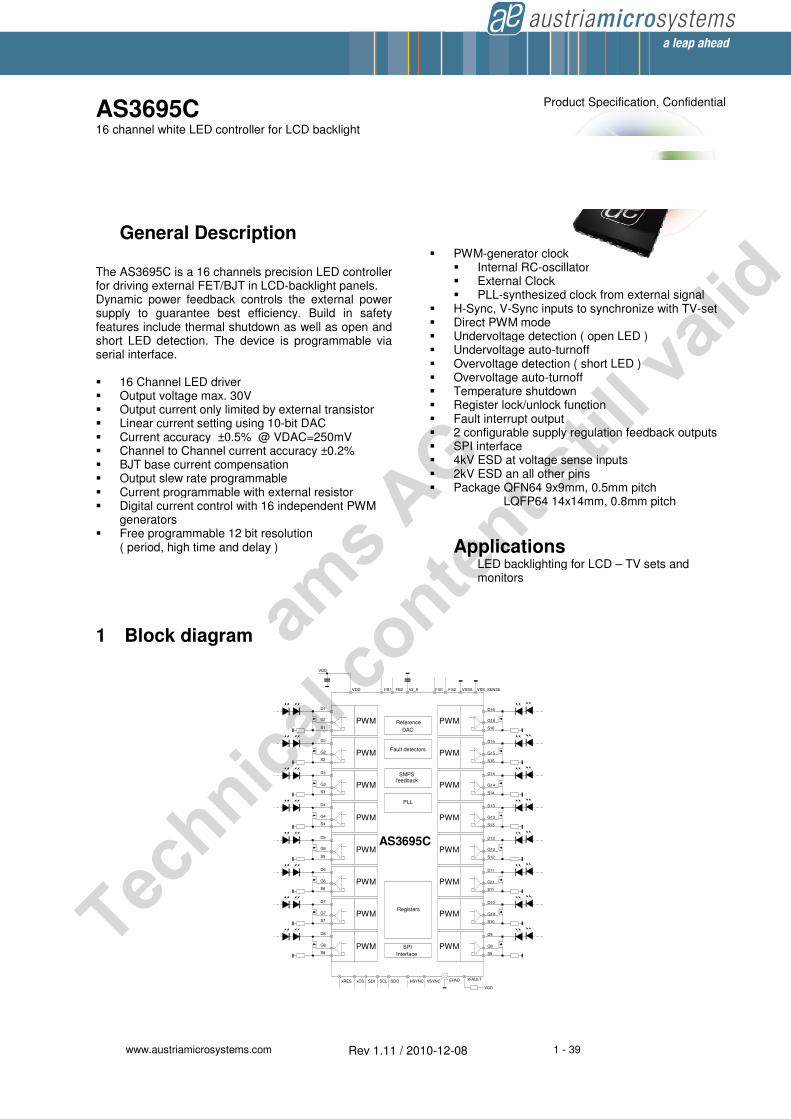
The AS3695C is a 16 channels precision LED controllfor driving external FET/BJT in LCD-Dynamic power feedback controls the extsupply to guarantee best efficiency. Build in safety features include thermal shutdown as well as open and short LED detection. The device is programmable via serial interface.
16 Channel LED driver Output voltage max. 30V Output current only limited by external Linear current setting using 10-bit DAC Current accuracy ±0.5% @ VDAC=250mV Channel to Channel current accuracy ±0.2% BJT base current compensation Output slew rate programmable Current programmable with external resistor Digital current control with 16 independent PWM
generators Free programmable 12 bit resolution
( period, high time and delay )
1 Block diagram
Rev 1.11 / 2010-12-08 1 - 39
16 channel white LED controller for LCD backlight
eneral Description
is a 16 channels precision LED controller -backlight panels.
Dynamic power feedback controls the external power best efficiency. Build in safety
include thermal shutdown as well as open and detection. The device is programmable via
Output current only limited by external transistor bit DAC
Current accuracy ±0.5% @ VDAC=250mV accuracy ±0.2%
BJT base current compensation Output slew rate programmable Current programmable with external resistor
ntrol with 16 independent PWM
12 bit resolution
Product Specification, Confidential
PWM-generator clock Internal RC-oscillator External Clock PLL-synthesized clock from external
H-Sync, V-Sync inputs to synchronize with TV Direct PWM mode Undervoltage detection ( open LED ) Undervoltage auto-turnoff Overvoltage detection ( short LED ) Overvoltage auto-turnoff Temperature shutdown Register lock/unlock function Fault interrupt output 2 configurable supply regulation feedback outputs SPI interface 4kV ESD at voltage sense inputs 2kV ESD an all other pins Package QFN64 9x9mm, 0.5
LQFP64 14x14mm, 0.8
Applications LED backlighting for LCD monitors
AS3695C
PWM
D1
PWM
VDD V2_5
S1
xFAULT
VDD
VDD
xRES xCS
FB1 FB2 VSS_SENSEVSSA
SDI SCL SDO EPADHSYNC VSYNC
G1
PWM
D2
S2
G2
PWM
D3
S3
G3
PWM
D4
S4
G4
PWM
D5
S5
G5
PWM
D6
S6
G6
PWM
D7
S7
G7
PWM
D8
S8
G8
D16
S16
G16
PWM
D15
S15
G15
PWM
D14
S14
G14
PWM
D13
S13
G13
PWM
D12
S12
G12
PWM
D11
S11
G11
PWM
D10
S10
G10
PWM
D9
S9
G9SPI
Interface
Registers
SMPSfeedback
Fault detectors
Reference
DAC
Filt1 Filt2
PLL
39
Product Specification, Confidential
oscillator
synthesized clock from external signal Sync inputs to synchronize with TV-set
Undervoltage detection ( open LED ) turnoff
Overvoltage detection ( short LED ) turnoff
Temperature shutdown Register lock/unlock function
2 configurable supply regulation feedback outputs
kV ESD at voltage sense inputs 2kV ESD an all other pins
mm, 0.5mm pitch LQFP64 14x14mm, 0.8mm pitch
LED backlighting for LCD – TV sets and
ams A
G
Technica
l conten
t still
valid

AS3695C austriamicrosystems
www.austriamicrosystems.com Rev 1.11 / 2010-12-08 2 - 39
2 Typical application
( Epad )
FB2
VDD
VDD
SDI
Vref
16x Precision current sink
V2_5 VSS_Sense
Power Supply
Vin
Dyn
am
ic p
ow
er
co
ntr
ol
AS3695C
16 output
SPISCLK
xCS
16 x PWM
SDO
xFault
FB1HSYNC
VSYNC
xRES
S1
Vdcdc
Cfb
Rfb
VDD
D1
4.7uF
2.2uF
channels
10uF
S16
VSSAVSSAD
yn
am
ic p
ow
er
co
ntr
ol
Rfb
Cfb
10uF
G1 S2D2 G2 S15D15 G15 D16 G16
Filt1
PLLFilt2
C0R1
C1 ams A
G
Technica
l conten
t still
valid

AS3695C austriamicrosystems
www.austriamicrosystems.com Rev 1.11 / 2010-12-08 3 - 39
3 Electrical Characteristics
3.1 Absolute Maximum Ratings
Stresses beyond those listed may cause permanent damage to the device. These are stress ratings only, and functional operation of the device at these or any other conditions beyond those indicated in Section “Electrical Characteristics” is not implied. Exposure to absolute maximum rating conditions for extended periods may affect device reliability.
Symbol Parameter Min Max Unit Note
Electrical Parameters
VDDMAX Supply voltage -0.3 7 V Applicable for pin VDD
VIN_2.5V Maximum voltage -0.3 2.8 V Applicable for 2.5V pins (1)
VIN_5V Maximum voltage -0.3 VDD
+0.3V V Applicable for 5V pins
(2)
VIN_30V Maximum voltage -0.3 30 V Applicable for 30V pins (3)
Ilatch Latch-Up immunity -100 +100 mA Norm: JEDEC 78
Electrostatic Discharge
VESD_LV Electrostatic Discharge on all 5V
pins (1)
-2000 2000 V Norm: MIL 883 E Method 3015
Human body model
VESD_HV Electrostatic Discharge on 30V
pins (2)
against GND -4000 4000 V Norm: MIL 883 E Method 3015
Human body model
Continous Power Dissipation ( TA = +70°C )
Continous Power Dissipation 1.5 W PT(4)
for QFN64 Package
Continous Power Dissipation
Derating factor 33
mW/°C
PDERATE (5)
Temperature Ranges and Storage Conditions
TJ Junctions temperature +150 °C
TSTRG Storage Temperature Range -55 +150 °C
TBODY Package body temperature 260 °C
The reflow peak soldering temperature (body temperature) specified is in accordance with IPC/JEDEC J-STD-020 “Moisture/Reflow SensitivityClassification for Non-Hermetic Solid State Surface Mount Devices”. The lead finish for Pb-free leaded packages is matte tin (100% Sn).
Humidity non condensing 5 85 %
Moisture Sensitive Level 3 Represents a max. floor life time of 168h
Note: (1) Pins V2_5, Filt1, Filt2
(2) Pins xRES, SDI, SCLK, SDO, xCS, VSYNC, HSYNC, VDD, xFault, FB1, FB2, G1-G16, S1-D16 (3) Pins D1 – D16 (4) Depending on actual PCB layout and PCB used
(5) PDERATE derating factor changes the total continuous power dissipation (PT) if the ambient temperature is not 70ºC. Therefore for e.g. TA=85ºC calculate PT at 85ºC = PT - PDERATE x (85ºC - 70ºC)
3.2 Operating Conditions
3.2.1 General
Symbol Parameter Conditions Min Typ Max Unit
Rthja Thermal resistance
junction – ambient See chapter “Thermal characteristics” °C/W
Tcase Case Temperatur -20 85 °C
ams A
G
Technica
l conten
t still
valid
AS3695C austriamicrosystems
www.austriamicrosystems.com Rev 1.11 / 2010-12-08 4 - 39
Symbol Parameter Conditions Min Typ Max Unit
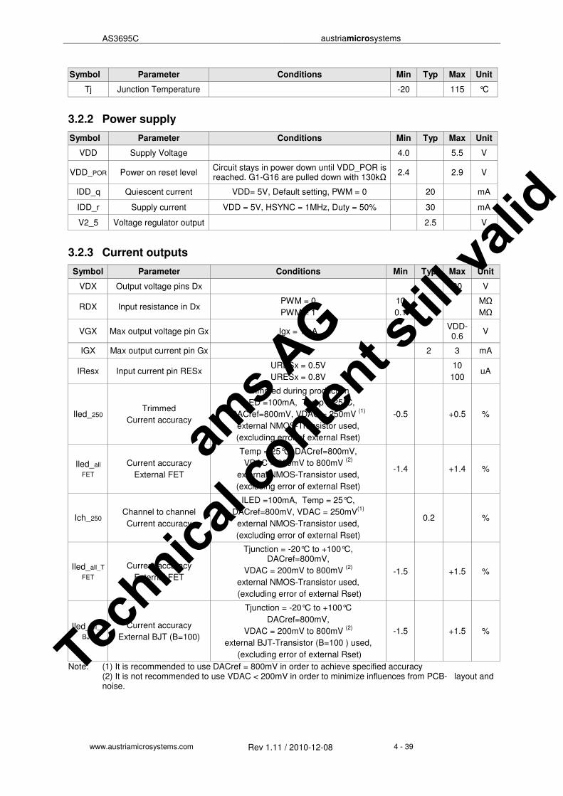
Tj Junction Temperature -20 115 °C
3.2.2 Power supply
Symbol Parameter Conditions Min Typ Max Unit
VDD Supply Voltage 4.0 5.5 V
VDD_POR Power on reset level Circuit stays in power down until VDD_POR is reached. G1-G16 are pulled down with 130kΩ
2.4 2.9 V
IDD_q Quiescent current VDD= 5V, Default setting, PWM = 0 20 mA
IDD_r Supply current VDD = 5V, HSYNC = 1MHz, Duty = 50% 30 mA
V2_5 Voltage regulator output 2.5 V
3.2.3 Current outputs
Symbol Parameter Conditions Min Typ Max Unit
VDX Output voltage pins Dx 30 V
RDX Input resistance in Dx PWM = 0
PWM = 1
10
0.1
MΩ
MΩ
VGX Max output voltage pin Gx Igx = 1mA VDD-0.6
V
IGX Max output current pin Gx 2 3 mA
IResx Input current pin RESx URESx = 0.5V
URESx = 0.8V
10
100 uA
Iled_250 Trimmed
Current accuracy
Trimmed during production
ILED =100mA, Temp = 25°C,
DACref=800mV, VDAC = 250mV (1)
external NMOS-Transistor used,
(excluding error of external Rset)
-0.5 +0.5 %
Iled_all
FET
Current accuracy
External FET
Temp = 25°C, DACref=800mV,
VDAC = 200mV to 800mV (2)
external NMOS-Transistor used,
(excluding error of external Rset)
-1.4 +1.4 %
Ich_250 Channel to channel
Current accuracy
ILED =100mA, Temp = 25°C,
DACref=800mV, VDAC = 250mV(1)
external NMOS-Transistor used,
(excluding error of external Rset)
0.2 %
Iled_all_T
FET
Current accuracy
External FET
Tjunction = -20°C to +100°C, DACref=800mV,
VDAC = 200mV to 800mV (2)
external NMOS-Transistor used,
(excluding error of external Rset)
-1.5 +1.5 %
Iled_all_T
BJT
Current accuracy
External BJT (B=100)
Tjunction = -20°C to +100°C
DACref=800mV,
VDAC = 200mV to 800mV (2)
external BJT-Transistor (B=100 ) used,
(excluding error of external Rset)
-1.5 +1.5 %
Note: (1) It is recommended to use DACref = 800mV in order to achieve specified accuracy (2) It is not recommended to use VDAC < 200mV in order to minimize influences from PCB- layout and noise.
ams A
G
Technica
l conten
t still
valid

AS3695C austriamicrosystems
www.austriamicrosystems.com Rev 1.11 / 2010-12-08 5 - 39
3.2.4 Feedback circuit, fault detectors
Symbol Parameter Conditions Min Typ Max Unit
IFBmax Feedback current
maximum 200 uA
RFBmin Minim output resistance VDx = 0.2V 200 800 Ω
IFB_g FB transconductance IFB_g = ∆IFB/ ∆VDx -2 mA/V
VFB Feedback voltage trip
point
Programmable
Tolerance ±10%
0.6
0.8
1.0
VDAC
+0.35
V
Vshort Short LED detection
voltage at Pin Dx
Programmable
Tolerance ±1.2V
2
3
4
5
6
7
8
9
10
11
12
V
V
V
V
V
V
V
V
V
V
V
Vopen Open LED detection
Voltage at Pin Sx
Programmable
Tolerance ±10%
50
100
200
VDAC/2
mV
mV
mV
V
Tovtemp Over temperature limit 130 140 150 °C
Thyst Over termperature
hysteresis 10 °C
3.2.5 PWM-generators
Symbol Parameter Conditions Min Typ Max Unit
fOSC Internal Clock for PWM 400 500 600 kHz
fHSYNC HSYNC frequency 100 2000 kHz
fVSYNC VSYNC frequency 60 480 Hz
fPLL PLL frequency 125 2000 kHz
3.2.6 Digital pins
Symbol Parameter Min Typ Max Unit Note
VIH High Level Input voltage 1.3 VDD V
VIL Low Level Input voltage -0.3 0.8 V
VoH High Level output voltage VDD-0.3 V I=mA
VoL Low Level output voltage VDD-0.3
V I=mA
VoL_PD Low level output voltage open
drain outputs
VDD-0.3
V I=mA
R_pu Input resistance PullUp inputs 300 kΩ
ams A
G
Technica
l conten
t still
valid

AS3695C austriamicrosystems
www.austriamicrosystems.com Rev 1.11 / 2010-12-08 6 - 39
Symbol Parameter Min Typ Max Unit Note
R_pd Input resistance PullDown inputs 300 kΩ
3.2.7 SPI-timings
Symbol Parameter Min Typ Max Unit Note
fsclk SCLK frequency 0 10 MHz
t1 xCS setup time 50 ns
t2 xCS hold time 100 ns
t3 xCS disable time 100 ns
t4 SDI setup time 5 ns
t5 SDI hold time 5 ns
t6 SCLK rise time 5 ns
t7 SCLK fall time 5 ns
t8 SCLK low time 40 ns
t9 SCLK high time 40 ns
t10 output valid from SCLK low 10 ns
SPI-input timing
SPI-output timing
xCS
SCLK
SDI
SDO
MSB IN LSB IN
1
4 5
2
3
6 7
HI-Z HI-Z
xCS
SCLK
SDI
SDO MSB OUT
9
10
2
Don't care
8
HI-Z
ams A
G
Technica
l conten
t still
valid
AS3695C austriamicrosystems
www.austriamicrosystems.com Rev 1.11 / 2010-12-08 7 - 39
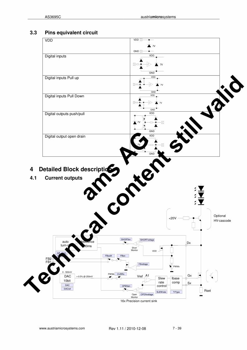
3.3 Pins equivalent circuit
VDD
Digital inputs
Digital inputs Pull up
Digital inputs Pull Down
Digital outputs push/pull
Digital output open drain
4 Detailed Block description
4.1 Current outputs
7V
VDD
GND
7V
VDD
GND
7V
VDD
GND
7V
VDD
GND
7V
VDD
GND
7V
VDD
GND
Sx
Dx
FB2
16x Precision current sink
VrefPWMx
Open
Monitor
FB1
<20V
ShortMonitor
SHORTvoltage
FBenFBselX
FBvoltage
OPENvoltageSLEWrate
CURRxA1
DAC
0 - 500mV
+-0.5% @ 250mV
toff_short
10bit
DACSlew
controlrate
autoturn-off
debounce
100ms
Optional
HV-cascode
Rset
SHORTen
OPENen
PWMx
VDD
Gx
toff_open
DACref
Ibase
comp
TrType
ams A
G
Technica
l conten
t still
valid

AS3695C austriamicrosystems
www.austriamicrosystems.com Rev 1.11 / 2010-12-08 8 - 39
4.1.1 Precision current sink
All current sinks are built with an internal error amplifier A1 and an external power transistor. The external transistor can either be a NMOS or a NPN bipolar transistor. The driving current capability of the output amplifier is 2mA. For low EMI radiation the slew rate of the amplifier output voltage can be adjusted between 1us and 9us
4.1.2 Power supply feedback
The voltage on the pins “Dx” is monitored to adjust the DCDC output voltage. If this voltage is lower than “FBvoltage” a comparator turns on a NMOS transistor which is able to control the output voltage of the external power supply via pin FB1 or pin FB2. The feedback comparator can be assigned to either FB1 or FB2. The power supply feedback can be turned off for all channels by the flag “FBen”. If an output is turned off with the corresponding bit in the CUR_ON_1/2 -registers, the feedback function of this output is also automatically turned off.
4.1.3 Open LED detection
If a LED-string is broken the voltage at the current setting resistor goes below “OPENvoltage”. This status is detected by a comparator and if this status lasts longer than 100ms a fault is indicated and optionally the output and the corresponding power feedback function is turned off. This feature can also be used for external resistor short detection during production. For proper detection the PWM high time has to be longer than 50us.
4.1.4 Short LED detection
Shorted LEDs in a LED-string will cause higher voltage at pin “Dx”. A higher voltage during PWM=1 is detected by a comparator and will trigger a “short LED detection” fault. The duration of the fault is accumulated and if the time exceeds 100ms a fault is indicated and optionally the output is turned off. If the high-time of the waveform is shorter than 100ms it will take more periods to trigger this fault. For proper detection the PWM high time has to be longer than 50us.
4.1.5 Fault detection
If an Open-LED or Short-LED condition is detected the fault-signal is debounced with an internal 100ms clock. This means that the fault will be indicated in the OPENLED or SHORTLED registers between 100ms and 200ms. In order to clear the bit in these registers a “1” has to be written.
4.1.6 DAC
The reference voltage for the output stage is generated by an internal 10-bit DAC. The DAC reference can be selected between 500mV and 800mV depending on register settings. The DAC is trimmed during production with DACref = 800mV to guarantee an output current accuracy of ±0.5% on every current output.
D Q
PWMx
Delay
20us/40us
500kHz
FAULT
D Q1
100ms
R
S Q
R
CLEAR FAULT BIT BY WRITING
OPENLED
SHORTLEDregisters
To STATUS register
From other
fault bits
1 to REGISTER
ams A
G
Technica
l conten
t still
valid

AS3695C austriamicrosystems
www.austriamicrosystems.com Rev 1.11 / 2010-12-08 9 - 39
The DAC output voltage can be calculated with:
DAC...10bit data value DACref...DAC reference voltage 500mV to 800mV
4.1.7 Registers in current output stage
RegAddr: 0x01 CUR_ON_1
Bit
Name
Description
Default Acc ess
7:0 CURR1 - CURR8
Enables or disables current outputs 0...output OFF. Pulldown resistor to GND 1...output ON.
00000000 r/w
RegAddr: 0x02 CUR_ON_2
Bit
Name
Description
Default Acc ess
7:0 CURR9 - CURR16
Enables or disables current outputs 0...output OFF. Pulldown resistor to GND 1...output ON.
00000000 r/w
RegAddr: 0x03 Fault_1
Bit
Name
Description
Default Acc ess
7:3 Not used 00000 r/w
2 Toff_OverT Automatic Output turn off at overtemperture 0...Do not turn off current outputs on overtemperature 1... Turn off current outputs on overtemperature
1 r/w
1 Toff_Short Automatic Output turn off on short LED detection 0...Do not turn off current outputs on on short LED detection 1... Turn off current outputs on short LED detection
0 r/w
0 Toff_Open Automatic Output turn off on open LED detection 0...Do not turn off current outputs on on open LED detection 1... Turn off current outputs on open LED detection
0 r/w
RegAddr: 0x04 Fault_2
Bit
Name
Description
Default Acc ess
7:6 OPENvoltage Trigger voltage for OPEN LED detection 00...50mV 01...100mV
00 r/w
DAC
Bandgap
800mV (trimmed)
reference
700mV
600mV
500mV
DACref
DACref
Ref
10bitDAC
VDAC
ams A
G
Technica
l conten
t still
valid

AS3695C austriamicrosystems
www.austriamicrosystems.com Rev 1.11 / 2010-12-08 10 - 39
10...200mV 11...VDAC/2
5:2 SHORTvoltage
Trigger voltage for SHORT LED detection 0000...2V 0001...3V 0010...4V 0011...5V 0100...6V 0101...7V 0110...8V 0111...9V 1000...10V 1001...11V 1010...12V 1011 to 1111 ...do not use
0000 r/w
1 SHORTen Enable short LED detection 0...SHORT detection OFF 1...SHORT detection ON
0 r/w
0 OPENen Enable open LED detection 0...OPEN detection OFF 1...OPEN detection ON
0 r/w
RegAddr: 0x05 Feedback
Bit
Name
Description
Default Acc ess
7:6 Not used 00 r/w
5:4 FBvoltage
Feedback regulator trip voltage.This voltage has to be adjusted if current is larger than 70mA or VDAC is higher than 0.25V 00...0.6V 01...0.8V 10...1.0V 11...V-DAC + 0.35V
00 r/w
3 FBboost Feedback boost option. FUNCTION DISABLED 0 r/w
2 TrType Type of external transistor 0...external FET. Base current compensation is off 1...external BJT. Base current compensation is on.
0 r/w
1 Not used 0 r/w
0 FBen
Enable Feedback function for all current outputs. 1...Feedback function enabled 0...Feedback function disabled Note: If a current output is disabled its Feedback function is automatically disabled.
0 r/w
RegAddr: 0x06 FB_SEL1
Bit
Name
Description
Default Acc ess
7:0 FBsel 1 - 8 Select FB-channel for current outputs 1 to 8 0...select FB channel FB1 1... select FB channel FB2
00000000 r/w
RegAddr: 0x07 FB_SEL2
Bit
Name
Description
Default Acc ess
7:0 FBsel 9 - 16 Select FB-channel for current outputs 9 to 16 0...select FB channel FB1 1... select FB channel FB2
00000000 r/w
RegAddr: 0x08 CURRctrl
Bit
Name
Description
Default Acc ess
7:6 Not used. 00 r/w
5:4 DACref
DAC reference voltage 00...500mV 01...600mV 10...700mV 11...800mV this reference is used at factory trimming
00 r/w
3:2 Not used 00 r/w
1:0 SLEWrate Select slew rate of output drivers 00...9us 01...6us
00 r/w
ams A
G
Technica
l conten
t still
valid

AS3695C austriamicrosystems
www.austriamicrosystems.com Rev 1.11 / 2010-12-08 11 - 39
10...3us 11...1us
RegAddr: 0x09 SHORTLED1
Bit
Name
Description
Default Acc ess
7:0 SHORTLED 1 - 8
Indicates short LED condition on outputs 1 to 8 0...no short LED detected 1... short LED detected
00000000 r/w
RegAddr: 0x0A SHORTLED2
Bit
Name
Description
Default Acc ess
7:0 SHORTLED 9 - 16
Indicates short LED condition on outputs 9 to 16 0...no short LED detected 1... short LED detected
00000000 r/w
RegAddr: 0x0B OPENLED1
Bit
Name
Description
Default Acc ess
7:0 OPENLED 1 - 8
Indicates open LED condition on outputs 1 to 8 0...no open LED detected 1... open LED detected
00000000 r/w
RegAddr: 0x0C OPENLED2
Bit
Name
Description
Default Acc ess
7:0 OPENLED 9 - 16
Indicates open LED condition on outputs 9 to 16 0...no open LED detected 1... open LED detected
00000000 r/w
RegAddr: DAC
0x0E 0x0D
Bit Bit Description Default Access
1:0 7:0 DAC[9:0] defines DADC output voltage DACvoltage = DAC[9:0]* DACref/1024
1000000000 r/w
4.2 PWM-generators
4.2.1 Clock and reset
The clock for the build in PWM-generators can be one of three different sources. 1. Internal RC oscillator with 500KHz +-20%
RefClk
Filt1
Filt2
NCdiv
PLL
125kHz - 2MHz
ACdiv
ODdiv
16 x PWM - generatorVsync60 - 480Hz
Hsync
PWMx
Reverse
Delay High Time
PWMper
Periode
SDO
SCLK
SDI
xCS
ClockSrc0
PWMext
:
:
PWM16del
clk
res
VSYNCedge
UpdateMode
VSYNCdet
RC-Oscillator500kHz ±20%
detect
Vsync
SPI
interface
PWM15del
PWM2del
PWM1del PWMrev
:
:
PWM16HT
PWM15HT
PWM2HT
PWM1HT
ClockSrc1
C0R1
C1
ams A
G
Technica
l conten
t still
valid
AS3695C austriamicrosystems
www.austriamicrosystems.com Rev 1.11 / 2010-12-08 12 - 39
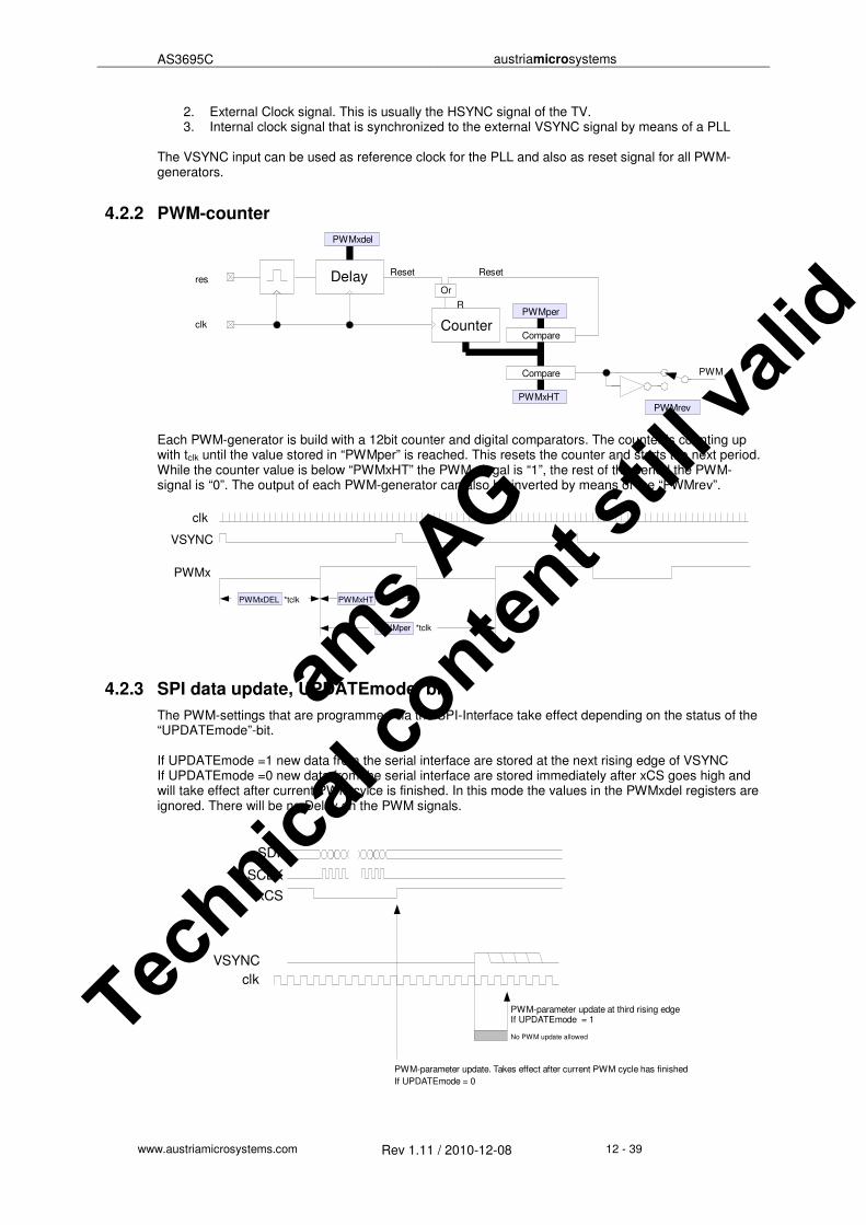
2. External Clock signal. This is usually the HSYNC signal of the TV. 3. Internal clock signal that is synchronized to the external VSYNC signal by means of a PLL
The VSYNC input can be used as reference clock for the PLL and also as reset signal for all PWM-generators.
4.2.2 PWM-counter
Each PWM-generator is build with a 12bit counter and digital comparators. The counter is counting up with tclk until the value stored in “PWMper” is reached. This resets the counter and starts the next period. While the counter value is below “PWMxHT” the PWM-singal is “1”, the rest of the period the PWM-signal is “0”. The output of each PWM-generator can also be inverted by means of the “PWMrev”.
4.2.3 SPI data update, UPDATEmode bit
The PWM-settings that are programmed via the SPI-Interface take effect depending on the status of the “UPDATEmode”-bit. If UPDATEmode =1 new data from the serial interface are stored at the next rising edge of VSYNC If UPDATEmode =0 new data from the serial interface are stored immediately after xCS goes high and will take effect after current PWM cylce is finished. In this mode the values in the PWMxdel registers are ignored. There will be no Delay on the PWM signals.
Delay
Counter
Compare
R
Resetres
clkCompare
Or
PWM
Reset
PWMper
PWMxdel
PWMrevPWMxHT
PWMxHTPWMxDEL
PWMper
VSYNC
PWMx
*tclk *tclk
*tclk
clk
PWM-parameter update at third rising edge
VSYNC
clk
SCLK
SDI
xCS
PWM-parameter update. Takes effect after current PWM cycle has finished
If UPDATEmode = 0
If UPDATEmode = 1
No PWM update allowed
ams A
G
Technica
l conten
t still
valid

AS3695C austriamicrosystems
www.austriamicrosystems.com Rev 1.11 / 2010-12-08 13 - 39
The PWMxHT-values are double buffered. HighTime values for the next VSYNC can be written even when the current HighTime is not finished.
4.2.4 PWM direct control
The internal signals PWMx can also be direct applied at the VSYNC input if the bit PWMext=1.
4.2.5 VSYNC detect
The VSYNCdet=1 the VSYNC detector monitors the presence of a VSYNC siglnal. If If the VSYNC signal is missing for more than 100ms current outputs are temporary turned off.
4.2.6 VSYNC duration
Since the VSYNC input is connected to an edge detector, there is no restriction on the duration of the VSYNC pulse.
ams A
G
Technica
l conten
t still
valid
AS3695C austriamicrosystems
www.austriamicrosystems.com Rev 1.11 / 2010-12-08 14 - 39
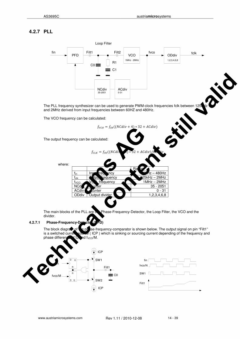
4.2.7 PLL
The PLL frequency synthesizer can be used to generate PWM-clock frequencies fclk between 125kHz and 2MHz derived from input frequencies between 60HZ and 480Hz. The VCO frequency can be calculated:
4 32 The output frequency can be calculated:
!" 4 32 /$ where:
Range
fin Input frequency 60 Hz – 480Hz
fclk Output frequency 125kHz – 2MHz
fVCO VCO frequency 1MHz – 2MHz
NCdiv counter 35 - 2051 ACdiv counter 0 - 31
ODdiv Output divider 1,2,3,4,6,8
The main blocks of the PLL are the Phase-Frequency-Detector, the Loop Filter, the VCO and the divider.
4.2.7.1 Phase-Frequency-Detector (PFD)
The block diagram of the phase-frequency-comparator is shown below. The output signal on pin “Filt1” is a switched current source ( ICP ) which is sinking or sourcing current depending of the frequency and phase difference of fin and fVCO/M.
fin Filt1 Filt2VCO
NCdiv
fvco
35-2051
Loop Filter
ODdivfclk
PFD
1,2,3,4,6,81MHz - 2MHz
ACdiv0-31
C0R1
C1
fin
fvco/M
Filt1
SW1
SW2
D Q
R
D Q
RC0
ICP
ICP
fin
fvco/N
SW1
Filt1
ams A
G
Technica
l conten
t still
valid

AS3695C austriamicrosystems
www.austriamicrosystems.com Rev 1.11 / 2010-12-08 15 - 39
4.2.7.2 VCO
In VCO has an operating range between 1MHz and 2MHz. If lower clock frequencies are required the output divider ( ODdiv ) has to be used.
4.2.7.3 Loop filter
The output of the PFD charges a loop filter which is controlling the output frequency of the VCO. The loop filter determines the speed of the frequency lock and the remaining phase noise of the VCO output frequency. Example of a loop filter:
Calculation process for loop filter: Terms: fVCO...Desired fVCO frequency
fIN...Reference input frequency Icp...PFC output current 0.5uA KVCO...VCO sensitivity 2.5MHz/V
1. Determined dividing ratio: % &'(
)*
2. Calculate Bandwidth BW: +, -.
3. Calculate C1: /0"&'(
1234
5.57
4. Calculate R1: 8 .9:;<=°
?@A5
5. Calculate C0: 5
4.2.7.4 Calculation Examples:
Vsync
[Hz]
Resolution
[ bit ]
Fclk
[Hz]
Reg
0x61
Reg
0x62
Reg
0x63
C0
[nF]
R1
[kΩ]
C1
[nF]
50 12 204800 0xFC 0x03 0x05 18,7 510 187
60 12 245760 0xFC 0x02 0x04 17,3 459 173
100 11 204800 0xFC 0x01 0x05 9,3 510 93
100 12 409600 0xFC 0x01 0x03 9,3 510 93
120 10 122880 0xFC 0x00 0x05 13,0 306 130
120 11 245760 0x7C 0x01 0x04 8,7 459 87
120 12 491520 0x7C 0x01 0x02 8,7 459 87
200 10 204800 0xFC 0x00 0x05 4,7 510 47
200 11 409600 0xFC 0x00 0x03 4,7 510 47
200 12 819200 0xFC 0x00 0x01 4,7 510 47
240 10 245760 0xBC 0x00 0x04 4,3 459 43
240 11 491520 0xBC 0x00 0x02 4,3 459 43
240 12 983040 0xFC 0x00 0x01 3,2 612 32
400 10 409600 0x7C 0x00 0x03 2,3 510 23
400 11 819200 0x7C 0x00 0x01 2,3 510 23
400 12 1638400 0x7C 0x00 0x00 2,3 510 23
480 10 491520 0x5C 0x00 0x02 2,2 459 22
480 11 983040 0x7C 0x00 0x01 1,6 612 16
480 12 1966080 0x7C 0x00 0x00 1,6 612 16
Filt1 Filt2
C0R1
C1
ams A
G
Technica
l conten
t still
valid
AS3695C austriamicrosystems
www.austriamicrosystems.com Rev 1.11 / 2010-12-08 16 - 39
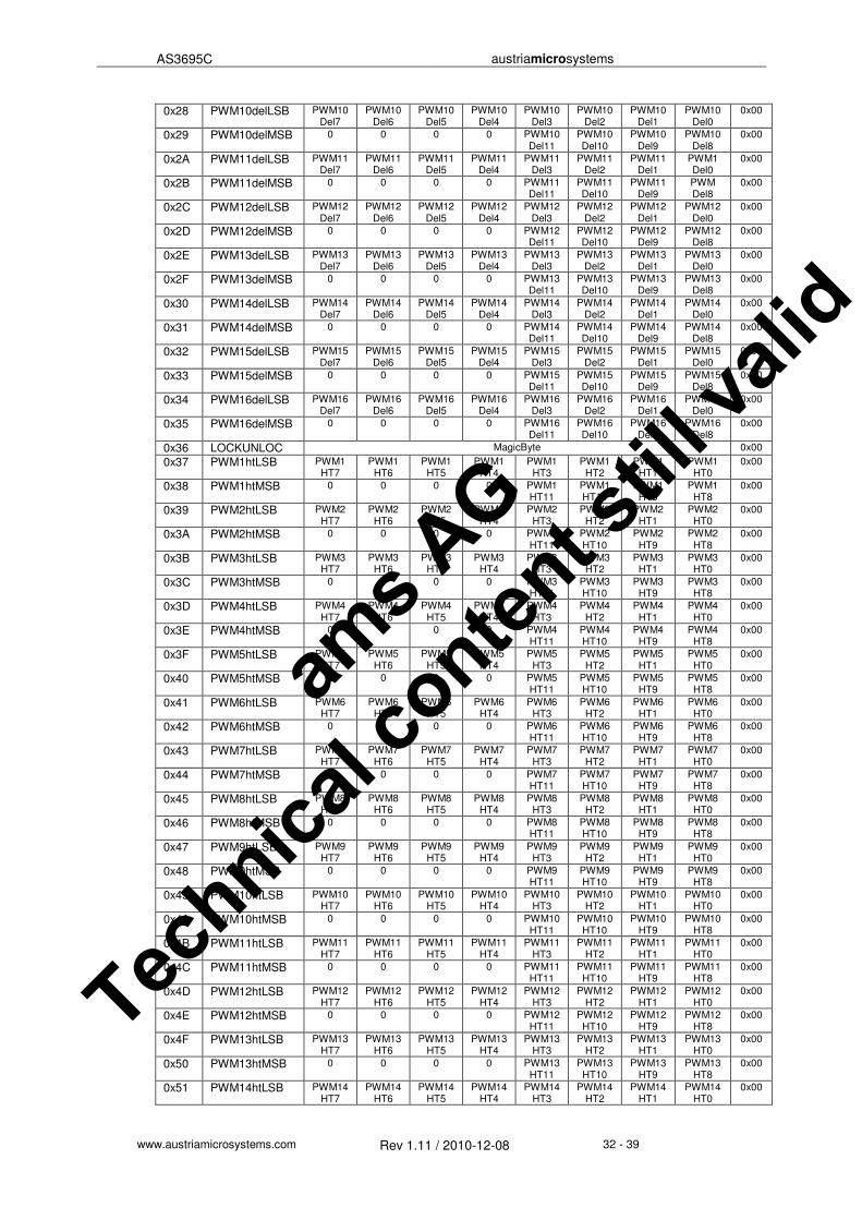
4.2.8 Registers in PWM-generators
RegAddr: 0x11 PWMREV1
Bit
Name
Description
Default Acc ess
7:0 PWMrev 1 - 8
Selects PWM inverted operation for outputs 1 to 8 0...PWM normal 1... PWM inverted
00000000 r/w
RegAddr: 0x12 PWMREV2
Bit
Name
Description
Default Acc ess
7:0 PWMrev 9 - 16
Selects PWM inverted operation for outputs 9 to 16 0...PWM normal 1... PWM inverted
00000000 r/w
RegAddr: 0x13 PWMCTRL
Bit
Name
Description
Default Acc ess
7 FaultDetDly Sets delay time between PWM=1 and fault detection start 0...120us 1...60us
0 r/w
6 DelayStart
Defines when new PWM-Delay value takes effect 0...Delay values are updated every VSYNC pulse 1...Delay values are updated on the next VSYNC pulse only if HighTime or Delay value has been changed.
0 r/w
5 ClockSrc1 Clock source for internal PWM-generators 0..internal RC oscillator or HSYNC ( depending on ClockSrc0 ) 1...PLL output
0 r/w
4 VSYNCdet
Enable VSYNC detection 0...VSYNC-detection OFF 1... VSYNC-detection ON. All current outpts are turned off if VSYNC signal is missing for 100ms
0 r/w
3 VSYNCedge Defines VSYNC trigger edge 0...VSYNC trigger on rising edge 1...VSYNC trigger on falling edge
0 r/w
2 PWMext Select external or internal PWM signal 0...PWM signal is generated internally 1...PWM signal is applied externally at pin VSYNC
0 r/w
1 UpdateMode Defines when internal registers are updated 0...Registers updated with rising edge of xCS 1...Registers updated with next VSYNC-edge
0 r/w
0 ClockSrc0
Clock source for internal PWM-generators 0..internal RC oscillator 1...External Pin HSYNC Note: This bit only takes effect when ClockSrc1 = 0
0 r/w
RegAddr: PWMperiod 0x15 0x14
Bit Bit Description Default Access
3:0 7:0 PWMper[11:0] sets PWM period 0x00, 0x00 r/w
RegAddr: PWM1delay 0x17 0x16
Bit Bit Description Default Access
3:0 7:0 PWM1del[11:0] sets PWM1 delay 0x00, 0x00 r/w
RegAddr: PWM2delay
0x19 0x18
Bit Bit Description Default Access
3:0 7:0 PWM2del[11:0] sets PWM2 delay 0x00, 0x00 r/w
RegAddr: PWM3delay
0x1B 0x1A
ams A
G
Technica
l conten
t still
valid

AS3695C austriamicrosystems
www.austriamicrosystems.com Rev 1.11 / 2010-12-08 17 - 39
Bit Bit Description Default Access
3:0 7:0 PWM3del[11:0] sets PWM3 delay 0x00, 0x00 r/w
RegAddr: PWM4delay
0x1D 0x1C
Bit Bit Description Default Access
3:0 7:0 PWM4del[11:0] sets PWM4 delay 0x00, 0x00 r/w
RegAddr: PWM5delay
0x1F 0x1E
Bit Bit Description Default Access
3:0 7:0 PWM5del[11:0] sets PWM5 delay 0x00, 0x00 r/w
RegAddr: PWM6delay
0x21 0x20
Bit Bit Description Default Access
3:0 7:0 PWM6del[11:0] sets PWM6 delay 0x00, 0x00 r/w
RegAddr: PWM7delay 0x23 0x22
Bit Bit Description Default Access
3:0 7:0 PWM7del[11:0] sets PWM7 delay 0x00, 0x00 r/w
RegAddr: PWM8delay 0x25 0x24
Bit Bit Description Default Access
3:0 7:0 PWM8del[11:0] sets PWM8 delay 0x00, 0x00 r/w
RegAddr: PWM9delay
0x27 0x26
Bit Bit Description Default Access
3:0 7:0 PWM9del[11:0] sets PWM9 delay 0x00, 0x00 r/w
RegAddr: PWM10delay 0x29 0x28
Bit Bit Description Default Access
3:0 7:0 PWM10del[11:0] sets PWM10 delay 0x00, 0x00 r/w
RegAddr: PWM11delay 0x2B 0x2A
Bit Bit Description Default Access
3:0 7:0 PWM11del[11:0] sets PWM11 delay 0x00, 0x00 r/w
RegAddr: PWM12delay 0x2D 0x2C
Bit Bit Description Default Access
3:0 7:0 PWM12del[11:0] sets PWM12 delay 0x00, 0x00 r/w
RegAddr: PWM13delay 0x2F 0x2E
Bit Bit Description Default Access
3:0 7:0 PWM13del[11:0] sets PWM13 delay 0x00, 0x00 r/w
RegAddr: PWM14delay 0x31 0x30
Bit Bit Description Default Access
3:0 7:0 PWM14del[11:0] sets PWM14 delay 0x00, 0x00 r/w
ams A
G
Technica
l conten
t still
valid

AS3695C austriamicrosystems
www.austriamicrosystems.com Rev 1.11 / 2010-12-08 18 - 39
RegAddr: PWM15delay
0x33 0x32
Bit Bit Description Default Access
3:0 7:0 PWM15del[11:0] sets PWM15 delay 0x00, 0x00 r/w
RegAddr: PWM16delay
0x35 0x34
Bit Bit Description Default Access
3:0 7:0 PWM16del[11:0] sets PWM16 delay 0x00, 0x00 r/w
RegAddr: 0x36 LOCKUNLOCK
Bit
Name
Description
Default Acc ess
7:0 LOCKUNLOCK
MagicByte to lock and unlock writing and reading of registers Writing into register: 0xCX...unlock register Group1. Writing enabled 0xXA...unlock register Group2. Writing enabled 0xCA...unlock register Group1 and Group2. Writing enabled 0xAX...lock register Group1. Writing disabled 0xXC...lock register Group2. Writing disabled 0xAC...lock register Group1 and Group2. Writing disabled X...don’t care. All other values do not change the status of lockunlock. Reading from register: 0x00.... Group1 and Group2 are locked 0x01...Group1 is unlocked 0x02...Group2 is unlocked 0x03...Group1 and Group2 are unlocked
0x00 r/w
RegAddr: PWM1hightime
0x38 0x37
Bit Bit Description Default Access
3:0 7:0 PWM1HT[11:0] sets PWM1 high time 0x00, 0x00 r/w
RegAddr: PWM2hightime 0x3A 0x39
Bit Bit Description Default Access
3:0 7:0 PWM2HT[11:0] sets PWM2 high time 0x00, 0x00 r/w
RegAddr: PWM3hightime 0x3C 0x3B
Bit Bit Description Default Access
3:0 7:0 PWM3HT[11:0] sets PWM3 high time 0x00, 0x00 r/w
RegAddr: PWM4hightime 0x3E 0x3D
Bit Bit Description Default Access
3:0 7:0 PWM4HT[11:0] sets PWM4 high time 0x00, 0x00 r/w
RegAddr: PWM5hightime 0x40 0x3F
Bit Bit Description Default Access
3:0 7:0 PWM5HT[11:0] sets PWM5 high time 0x00, 0x00 r/w
RegAddr: PWM6hightime 0x42 0x41
Bit Bit Description Default Access
3:0 7:0 PWM6HT[11:0] sets PWM6 high time 0x00, 0x00 r/w
ams A
G
Technica
l conten
t still
valid

AS3695C austriamicrosystems
www.austriamicrosystems.com Rev 1.11 / 2010-12-08 19 - 39
RegAddr: PWM7hightime
0x44 0x43
Bit Bit Description Default Access
3:0 7:0 PWM7HT[11:0] sets PWM7 high time 0x00, 0x00 r/w
RegAddr: PWM8hightime
0x46 0x45
Bit Bit Description Default Access
3:0 7:0 PWM8HT[11:0] sets PWM8 high time 0x00, 0x00 r/w
RegAddr: PWM9hightime
0x48 0x47
Bit Bit Description Default Access
3:0 7:0 PWM9HT[11:0] sets PWM9 high time 0x00, 0x00 r/w
RegAddr: PWM10hightime
0x4A 0x49
Bit Bit Description Default Access
3:0 7:0 PWM10HT[11:0] sets PWM10 high time 0x00, 0x00 r/w
RegAddr: PWM11hightime
0x4C 0x4B
Bit Bit Description Default Access
3:0 7:0 PWM11HT[11:0] sets PWM11 high time 0x00, 0x00 r/w
RegAddr: PWM12hightime
0x4E 0x4D
Bit Bit Description Default Access
3:0 7:0 PWMHT12[11:0] sets PWM12 high time 0x00, 0x00 r/w
RegAddr: PWM13hightime
0x50 0x4F
Bit Bit Description Default Access
3:0 7:0 PWM13HT[11:0] sets PWM13 high time 0x00, 0x00 r/w
RegAddr: PWM14hightime 0x52 0x51
Bit Bit Description Default Access
3:0 7:0 PWM14HT[11:0] sets PWM14 high time 0x00, 0x00 r/w
RegAddr: PWM15hightime
0x54 0x53
Bit Bit Description Default Access
3:0 7:0 PWM15HT[11:0] sets PWM15 high time 0x00, 0x00 r/w
RegAddr: PWM16hightime 0x56 0x55
Bit Bit Description Default Access
3:0 7:0 PWM16HT[11:0] sets PWM16 high time 0x00, 0x00 r/w RegAddr: 0x61 PLLctrl1
Bit
Name
Description
Default Acc ess
7:0 NCdiv[7:0] PLL divider NCdiv low bits 0 - 7 00000000 r/w RegAddr: 0x62 PLLctrl2
Bit
Name
Description
Default Acc ess
7:3 ACdiv[4:0] PLL divider ACdiv 00000 r/w 2:0 NCdiv[10:8] PLL divider NCdiv high bits 8 - 10 000 r/w
ams A
G
Technica
l conten
t still
valid

AS3695C austriamicrosystems
www.austriamicrosystems.com Rev 1.11 / 2010-12-08 20 - 39
RegAddr: 0x63 PLLctrl3
Bit
Name
Description
Default Acc ess
7:6 00 r
5:3 ICP[2:0]
PLL charge pump output current Icp 000...0.5uA 001...1uA 010...2uA 011...4uA 100...8uA 101...8uA 110...8uA 111...8uA
000 r/w
2:0 ODdiv[2:0]
PLL divider ODdiv 000...div 1 001...div 2 010...div 3 011...div 4 100...div 6 101...div 8 110...div 8 111...div 8
000 r/w
4.2.9 PWM examples
HSYNC
VSYNC
SPI cmd
PWM1del = 20
PWMrev1= 0
PWMCTRL=0x03
PWMperiod = 100
PWM1ht = 40
0 20 40 60 80 100
ILED1
PWM2del = 30
PWMrev2= 0
PWM2ht = 40
ILED2
ILED3
PWM3del = 40
PWMrev3= 0
PWM3ht = 40
HSYNC
VSYNC
SPI cmd
PWM1del = 20
PWMrev1= 1
PWMCTRL=0x03
PWMperiod = 100
PWM1ht = 40
0 20 40 60 80 100
ILED1
PWM2del = 30
PWMrev2= 1
PWM2ht = 40
ILED2
ILED3
PWM3del = 40
PWMrev3= 1
PWM3ht = 40
ams A
G
Technica
l conten
t still
valid

AS3695C austriamicrosystems
www.austriamicrosystems.com Rev 1.11 / 2010-12-08 21 - 39
HSYNC
VSYNC
SPI cmd
PWM1del = 120
PWMrev1= 0
PWMCTRL=0x03
PWMperiod = 100
PWM1ht = 40
0 20 40 60 80 100
ILED1
PWM2del = 130
PWMrev2= 0
PWM2ht = 40
ILED2
ILED3
PWM3del = 140
PWMrev3= 0
PWM3ht = 40
120 140
HSYNC
VSYNC
SPI cmd
PWM1del = 20
PWMrev1= 0
PWMCTRL=0x03
PWMperiod = 20
PWM1ht = 15
0 20 40 60 80 100
ILED1
PWM2del = 30
PWMrev2= 0
PWM2ht = 10
ILED2
ILED3
PWM3del = 40
PWMrev3= 0
PWM3ht = 5
HSYNC
VSYNC
SPI cmd
PWM1del = 20
PWMrev1= 0
PWMCTRL=0x03
PWMperiod = 100
PWM1ht = 40
0 20 40 60 80
ILED1
PWM2del = 30
PWMrev2= 0
PWM2ht = 40
ILED2
ILED3
PWM3del = 40
PWMrev3= 0
PWM3ht = 40
PWM1del = 0
PWMrev1= 0
PWMCTRL=0x03
PWMperiod = 100
PWM1ht = 40
PWM2del = 40
PWMrev2= 0
PWM2ht = 40
PWM3del = 40
PWMrev3= 0
PWM3ht = 40
100 120 140ams A
G
Technica
l conten
t still
valid

AS3695C austriamicrosystems
www.austriamicrosystems.com Rev 1.11 / 2010-12-08 22 - 39
4.3 Power supply
4.4 Safety features
4.4.1 Temperature shutdown
If OTturnoff = 1 the outputs of the device are turned off when the die temperature reaches 140°C. If the die temperature goes below 130°C the outputs are turned on again.
4.4.2 xRES input
In addition to the build in power on reset circuit there is an external reset input “xRES” available. This gives the possibility to keep the outputs turned off until all blocks of the LED-driver circuits are fully working ( DCDC, MCU ... )
4.4.3 Register Lock/Unlock
To prevent wrong writing to registers due to noise on the serial interface a lock/unlock mechanism is implemented. Register 0x01, 0x02, 0x03, 0x04, 0x05, 0x06, 0x07, 0x08, 0x13 , 0x61, 0x62, 0x63 belong to Group1 and can only be written if Group1 is unlocked by the “LOCKUNLOCK”-byte (Reg: 0x36 ) Register 0x0D, 0x0E, 0x11, 0x12, 0x14, 0x15 belong to Group2 and can only be written if Group2 is unlocked by the “LOCKUNLOCK”-byte (Reg: 0x36 ) The default value of the Groups is locked.
4.5 Reference circuit
The reference circuit generates an internal supply voltage of 2.5V for the digital logic. RegAddr: 0x58 STATUS
Bit
Name
Description
Default Acc ess
7 STATnosync Sync detector status 0...no sync fault 1...sync fault. VSYNC was missed for > 100ms
0 r
6 STATOT Overtermperature status 0...no overtemperature 1...overtemperature
0 r
5 STATopen Status open LED detection 0...no open LED detected 1...opdn LED detected
0 r
4 STATshort Status short LED detection 0...no short LED detected 1...short LED detected
0 r
3 Not used 0
VDD
LDO2.5V digital supply
V2_5AGND
4.0V to 5.5V analog supply
POR Temp
xRESToff_OverT
ams A
G
Technica
l conten
t still
valid

AS3695C austriamicrosystems
www.austriamicrosystems.com Rev 1.11 / 2010-12-08 23 - 39
2 STATUVLO Status under voltage lockout detector 0...supply OK 1...supply voltage is to low
0 R
1:0 STATpower
Status of power supply monitor 00...no power supply 01...power supply is ramping up 10...power supply good 11...not used
10 r
ams A
G
Technica
l conten
t still
valid
AS3695C austriamicrosystems
www.austriamicrosystems.com Rev 1.11 / 2010-12-08 24 - 39
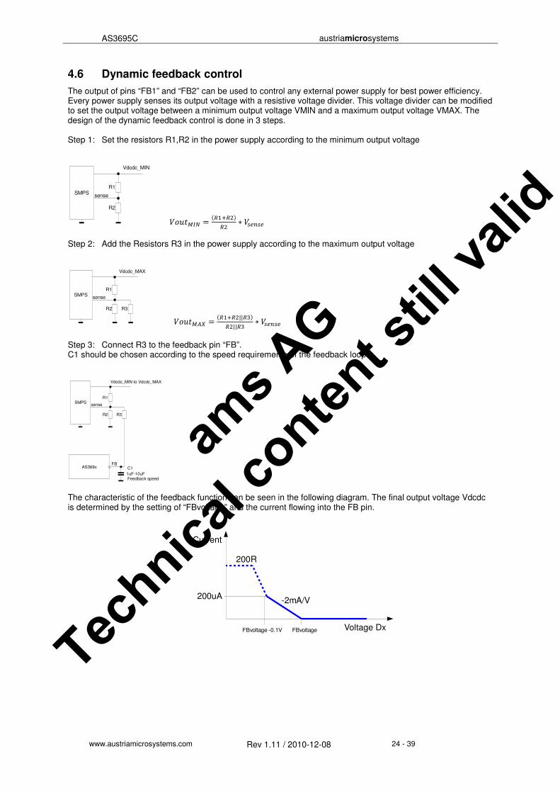
4.6 Dynamic feedback control
The output of pins “FB1” and “FB2” can be used to control any external power supply for best power efficiency. Every power supply senses its output voltage with a resistive voltage divider. This voltage divider can be modified to set the output voltage between a minimum output voltage VMIN and a maximum output voltage VMAX. The design of the dynamic feedback control is done in 3 steps. Step 1: Set the resistors R1,R2 in the power supply according to the minimum output voltage
BCD1 E FE
E G;G
Step 2: Add the Resistors R3 in the power supply according to the maximum output voltage
BCD1H E FE||EJ
E||EJ G;G
Step 3: Connect R3 to the feedback pin “FB”. C1 should be chosen according to the speed requirements of the feedback loop.
The characteristic of the feedback function can be seen in the following diagram. The final output voltage Vdcdc is determined by the setting of “FBvoltage” and the current flowing into the FB pin.
R1
R2
SMPS
Vdcdc_MIN
sense
R1
R2
SMPS
Vdcdc_MAX
sense
R3
AS369x
R1
R2
SMPS
Vdcdc_MIN to Vdcdc_MAX
sense
R3
FB
1uF-10uFFeedback speed
C1
CurrentInto FB-pin
200uA
Voltage DxFBvoltage
-2mA/V
FBvoltage -0.1V
200R
ams A
G
Technica
l conten
t still
valid
AS3695C austriamicrosystems
www.austriamicrosystems.com Rev 1.11 / 2010-12-08 25 - 39
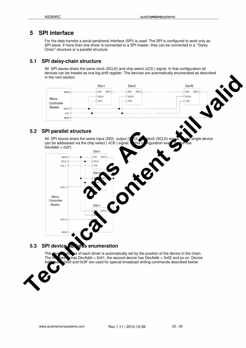
5 SPI interface
For the data transfer a serial peripheral interface (SPI) is used. The SPI is configured to work only as SPI slave. If more than one driver is connected to a SPI master, they can be connected in a “Daisy Chain”-structure or a parallel structure.
5.1 SPI daisy-chain structure
All SPI slaves share the same clock (SCLK) and chip select (xCS ) signal. In that configuration all devices can be treated as one big shift register. The devices are automatically enumerated as described in the next section.
5.2 SPI parallel structure
All SPI slaves share the same input (SDI) output (SDO) and clock (SCLK) signal. Every single device can be addressed via the chip select ( xCS ) signal. In this configuration every device has DevAddr = 0x01.
5.3 SPI device address enumeration
The device address of each driver is automatically set by the position of the device in the chain. The first device has DevAddr = 0x01, the second device has DevAddr = 0x02 and so on. Device Addresses 0x00 and 0x3F are used for special broadcast writing commands described below.
MOSI
MISO
SCLK
xCS
SCLK
xCS
SDI SDO
Micro
Controller
Master
Dev1
SCLK
xCS
SDI SDO
Dev2
SCLK
xCS
SDI SDO
DevN
MOSI
MISO
SCLK
xCS_N
SCLK
xCS
SDI SDO
Micro
Controller
Master
Dev1
SCLK
xCS
SDI SDO
Dev1
SCLK
xCS
SDI SDO
Dev1
xCS_2
xCS_1
ams A
G
Technica
l conten
t still
valid

AS3695C austriamicrosystems
www.austriamicrosystems.com Rev 1.11 / 2010-12-08 26 - 39
5.4 SPI protocol
5.4.1 Data types
When xCS=0 all slaves will be activated. The addressing and data section is organized in byte packages. Each message can be built with the following Bytes:
Device address:
Addresses a specific driver and defines protocol information
Bit Meaning Value B Broadcast B=1...Broadcast message to all devices
B=0...Normal message to one single device S Singlebyte S=0...Block data read or write
S=1...Single data transmission ( only one byte )
DevAddr[5:0] Device Address 0x00 Write same data to same register of all devices ( B=1 ) 0x01 to 0x3E. Device addresses for device 1 to 62 0x3F Write different data to same register of all devices ( B=1 )
Nr_of_data:
Defines the number of data bytes in the data frame if S=0 Bit Meaning Value
NrOfdata[7:0] Number of data bytes in frame
0x00 to 0xFF
Register_address:
Register address to be read or written
Bit Meaning Value RW Read/xWrite RW=0 write to reg address
RW=1 read from reg address RegAddr[6:0] Select register
address 0x00 to 0x60
Data:
Data Bit Meaning Value
data [7:0], Data 0x00 to 0xFF
SB DevAddr[5:0]
NrOfdata[7:0]
RW RegAddr[6:0]
data[7:0]
ams A
G
Technica
l conten
t still
valid
AS3695C austriamicrosystems
www.austriamicrosystems.com Rev 1.11 / 2010-12-08 27 - 39
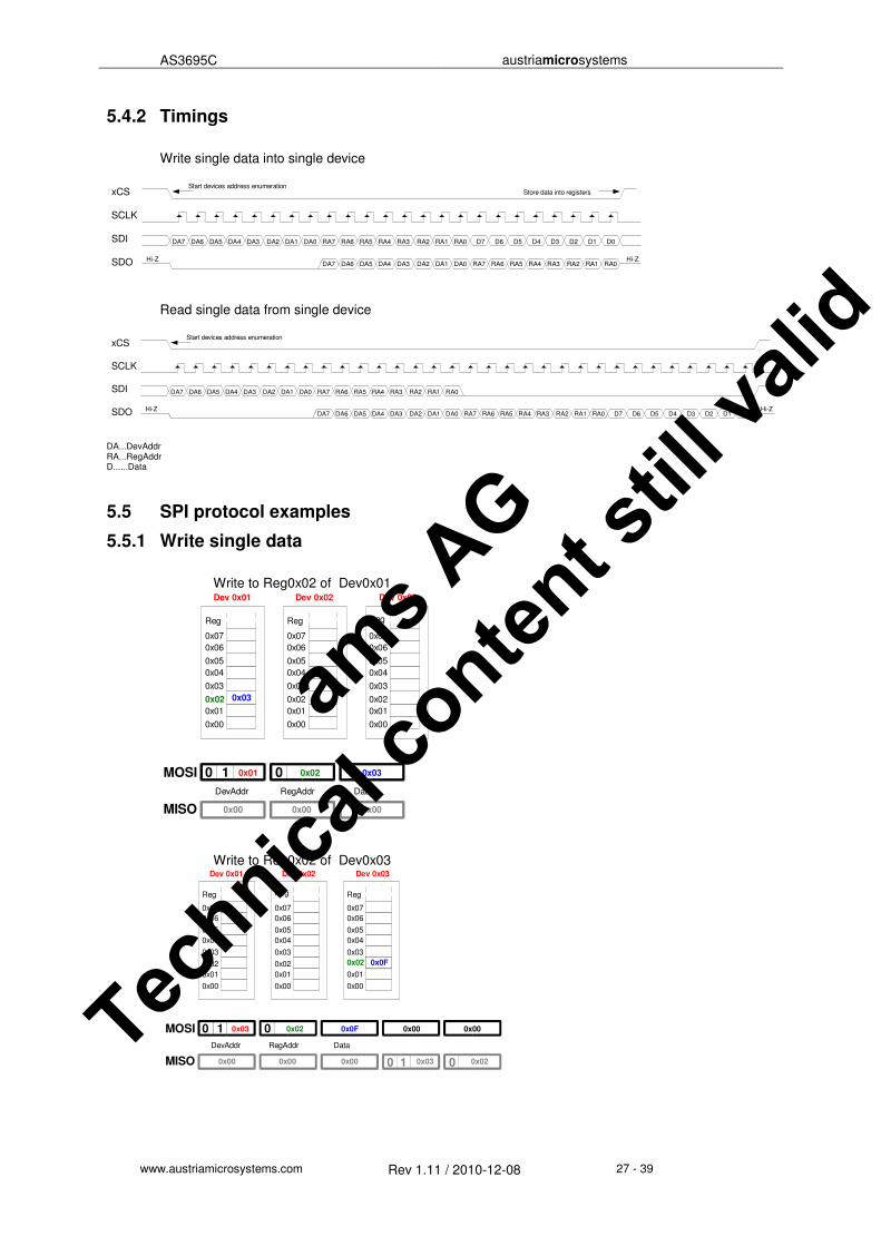
5.4.2 Timings
Write single data into single device
Read single data from single device
DA...DevAddr RA...RegAddr D......Data
5.5 SPI protocol examples
5.5.1 Write single data
Write to Reg0x02 of Dev0x01
Write to Reg0x02 of Dev0x03
SDI
SDO
SCLK
xCS
DA6
Start devices address enumerationStore data into registers
DA7 DA4DA5 DA2DA3 DA0DA1 RA6RA7 RA4RA5 RA2RA3 RA0RA1 D7 D6 D5 D4 D3 D2 D1 D0
Hi-Z Hi-ZDA6DA7 DA4DA5 DA2DA3 DA0DA1 RA6RA7 RA4RA5 RA2RA3 RA0RA1
SDI
SDO
SCLK
xCS
DA6
Start devices address enumeration
DA7 DA4DA5 DA2DA3 DA0DA1 RA6RA7 RA4RA5 RA2RA3 RA0RA1
D7 D6 D5 D4 D3 D2 D1 D0Hi-Z Hi-Z
DA6DA7 DA4DA5 DA2DA3 DA0DA1 RA6RA7 RA4RA5 RA2RA3 RA0RA1
0x00
Dev 0x01
0x01
0x02 0x03
0x03
0x04
0x05
0x06
0x07
10 0x01 0 0x02
DevAddr RegAddr
0x00
0x01
0x02
0x03
0x04
0x05
0x06
0x07
0x00
0x01
0x02
0x03
0x04
0x05
0x06
0x07
0x03
Data
Dev 0x02 Dev 0x03
Reg Reg Reg
MISO
MOSI
0x00 0x00 0x00
0x00
Dev 0x01
0x01
0x02
0x03
0x04
0x05
0x06
0x07
10 0x03 0 0x02
DevAddr RegAddr
0x00
0x01
0x02
0x03
0x04
0x05
0x06
0x07
0x00
0x01
0x02
0x03
0x04
0x05
0x06
0x07
0x0F
Data
Dev 0x02 Dev 0x03
Reg RegReg
0x00 0x00 0x00
0x0F
0x00 0x00
10 0x03 0 0x02MISO
MOSI
ams A
G
Technica
l conten
t still
valid

AS3695C austriamicrosystems
www.austriamicrosystems.com Rev 1.11 / 2010-12-08 28 - 39
5.5.2 Write N data
Write to Reg0x02 - Reg0x04 of Dev0x01
5.5.3 Write different data in same register of all devices ( single byte ) Set DevAdd = 0x3F
Write to Reg0x02 of Dev0x01 – Dev0x03
5.5.4 Write different data in same register of all devices ( multiple bytes ) Set DevAdd = 0x3F
Write to Reg0x02- Reg0x03 of Dev0x01 – Dev0x03
0x00
Dev 0x01
0x01
0x02 0x03
0x03 0x04
0x04 0x05
0x05
0x06
0x07
00 0x01 0x03 0 0x02
DevAddr NrOfBytes RegAddr
0x00
0x01
0x02
0x03
0x04
0x05
0x06
0x07
0x00
0x01
0x02
0x03
0x04
0x05
0x06
0x07
0x03
Data1
Dev 0x02 Dev 0x03
Reg Reg Reg
0x04
Data2
0x05
Data3
0x00 0x00 0x00 00 0x01 0x03 0 0x02MISO
MOSI
0x00
Dev 0x01
0x01
0x02 0x03
0x03
0x04
0x05
0x06
0x07
11 0x3F 0 0x02
DevAddr RegAddr
0x00
0x01
0x02 0x04
0x03
0x04
0x05
0x06
0x07
0x00
0x01
0x02 0x05
0x03
0x04
0x05
0x06
0x07
0x03
Data1
Dev 0x02 Dev 0x03
Reg Reg Reg
0x04
Data2
0x05
Data3
0x00 0x00 0x00 11 0x3F 0 0x02 0x03 0x04
0x00 0x00
MISO
MOSI
0x00
Dev 0x01
0x01
0x02 0x03
0x03 0x04
0x04
0x05
0x06
0x07
01 0x3F 0x02 0 0x02
DevAddr NrOfBytes RegAddr
0x00
0x01
0x02 0x05
0x03 0x06
0x04
0x05
0x06
0x07
0x00
0x01
0x02 0x07
0x03 0x08
0x04
0x05
0x06
0x07
0x03
Data1
Dev 0x02 Dev 0x03
Reg Reg Reg
0x04
Data2
0x05
Data3
0x00 0x00 0x00 01 0x3F 0x02 0 0x02 0x03 0x04
0x06 0x07
MISO
MOSI 0x00 0x00
0x06 0x070x05
0x08
Data3 Data5 Data6
ams A
G
Technica
l conten
t still
valid

AS3695C austriamicrosystems
www.austriamicrosystems.com Rev 1.11 / 2010-12-08 29 - 39
5.5.5 Write same data in same register of all devices ( single byte ) Set DevAdd = 0x00
Write to Reg0x02 of Dev0x01 – Dev0x03
5.5.6 Write same data in same register of all devices ( multiple bytes ) Set DevAdd = 0x00
Write to Reg0x02 - Reg0x04 of Dev0x01 – Dev0x03
0x00
Dev 0x01
0x01
0x02 0x03
0x03 0x04
0x04 0x05
0x05
0x06
0x07
01 0x00 0x03 0 0x02
DevAddr NrOfBytes RegAddr
0x00
0x01
0x02 0x03
0x03 0x04
0x04 0x05
0x05
0x06
0x07
0x00
0x01
0x02 0x03
0x03 0x04
0x04 0x05
0x05
0x06
0x07
0x03
Data1
Dev 0x02 Dev 0x03
Reg Reg Reg
0x04
Data2
0x05
Data3
0x00 0x00 0x00 01 0x00 0x03 0 0x02 0x03 0x04
0x00 0x00
MISO
MOSI
0x00
Dev 0x01
0x01
0x02 0x03
0x03
0x04
0x05
0x06
0x07
11 0x00 0 0x02
DevAddr RegAddr
0x00
0x01
0x02 0x03
0x03
0x04
0x05
0x06
0x07
0x00
0x01
0x02 0x03
0x03
0x04
0x05
0x06
0x07
0x03
Data1
Dev 0x02 Dev 0x03
Reg Reg Reg
0x00 0x00 11 0x00 0x02
0x00 0x00
MISO
MOSI
0x00
ams A
G
Technica
l conten
t still
valid
AS3695C austriamicrosystems
www.austriamicrosystems.com Rev 1.11 / 2010-12-08 30 - 39
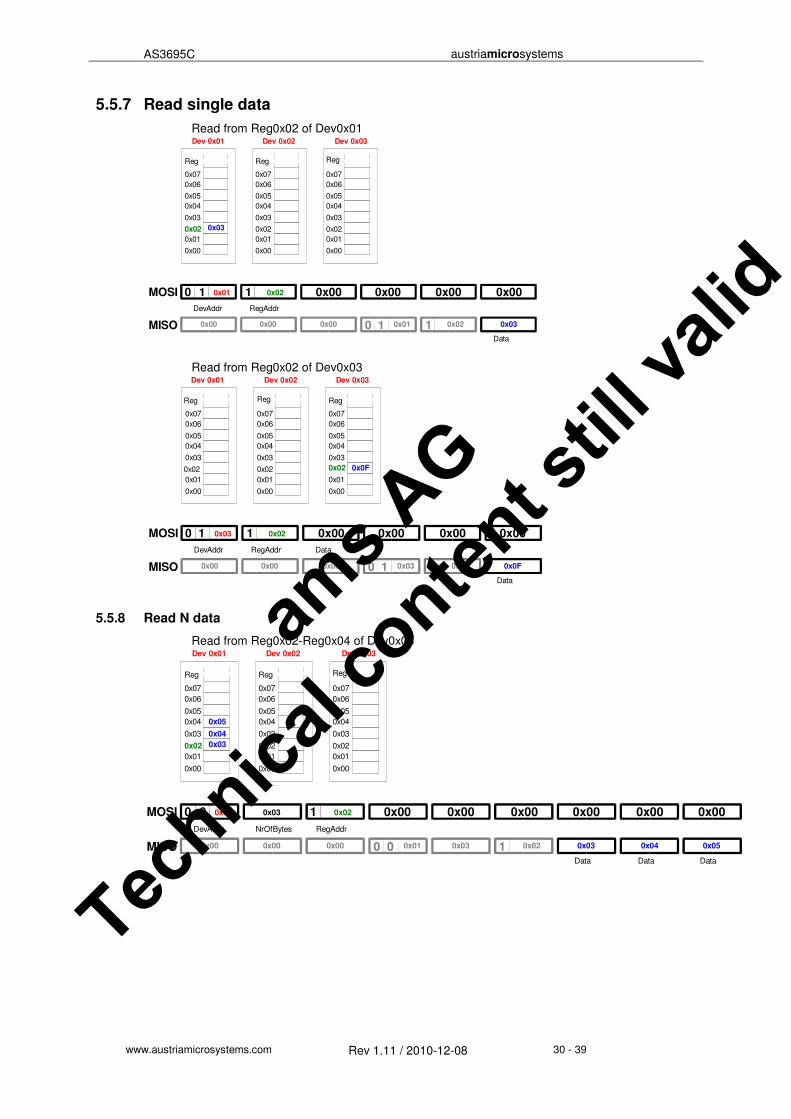
5.5.7 Read single data
Read from Reg0x02 of Dev0x01
Read from Reg0x02 of Dev0x03
5.5.8 Read N data
Read from Reg0x02-Reg0x04 of Dev0x03
0x00
Dev 0x01
0x01
0x02 0x03
0x03
0x04
0x05
0x06
0x07
10 0x01 1 0x02
DevAddr RegAddr
0x00
0x01
0x02
0x03
0x04
0x05
0x06
0x07
0x00
0x01
0x02
0x03
0x04
0x05
0x06
0x07
0x00
Data
Dev 0x02 Dev 0x03
Reg Reg Reg
0x00 0x00 0x030x00 10 0x01 1 0x02
0x00 0x00 0x00
MISO
MOSI
0x00
Dev 0x01
0x01
0x02
0x03
0x04
0x05
0x06
0x07
10 0x03 1 0x02
DevAddr RegAddr
0x00
0x01
0x02
0x03
0x04
0x05
0x06
0x07
0x00
0x01
0x02
0x03
0x04
0x05
0x06
0x07
Data
Dev 0x02 Dev 0x03
Reg RegReg
0x00 0x00 0x00
0x0F
0x00 0x00 0x00 0x00
Data
0x0F10 0x03 1 0x02MISO
MOSI
0x00
Dev 0x01
0x01
0x02 0x03
0x03 0x04
0x04 0x05
0x05
0x06
0x07
00 0x01 0x03 1 0x02
DevAddr NrOfBytes RegAddr
0x00
0x01
0x02
0x03
0x04
0x05
0x06
0x07
0x00
0x01
0x02
0x03
0x04
0x05
0x06
0x07
0x03
Data
Dev 0x02 Dev 0x03
Reg Reg Reg
0x04
Data
0x05
Data
0x00 0x00 0x00
0x00 0x00 0x000x00 0x00
00 0x01 0x03
0x00
1 0x02MISO
MOSI
ams A
G
Technica
l conten
t still
valid

AS3695C austriamicrosystems
www.austriamicrosystems.com Rev 1.11 / 2010-12-08 31 - 39
6 Register map
Registers can only be written if Group1 is UNLOCKED. Default = LOCKED
Registers can only be written if Group2 is UNLOCKED. Default = LOCKED
Addr Name D7 D6 D5 D4 D3 D2 D1 D0 Def
ault 0x00 Used for block writing
0x01 CUR_ON_1 Curr8 Curr7 Curr6 Curr5 Curr4 Curr3 Curr2 Curr1 0x00
0x02 CUR_ON_2 Curr16 Curr15 Curr14 Curr13 Curr12 Curr11 Curr10 Curr9 0x00
0x03 FAULT_1 Toff Otemp
Toff short
Toff open
0x04
0x04 FAULT_2 OPEN voltage
SHORT voltage
SHORT en
OPEN en
0x00
0x05 FEEDBACK FB voltage
FB boost
Tr Type
FB enable
0x00
0x06 FB_SEL1 FBsel8 FBsel7 FBsel6 FBsel5 FBsel4 FBsel3 FBsel2 FBsel1 0x00
0x07 FB_SEL2 FBsel16 FBsel15 FBsel14 FBsel13 FBsel12 FBsel11 FBsel10 FBsel9 0x00
0x08 CURRctrl DAC ref
Slew rate
0x00
0x09 SHORTLED1 Short8 Short7 Short6 Short5 Short4 Short3 Short2 Short1 0x00
0x0A SHORTLED2 Short16 Short15 Short14 Short13 Short12 Shor11 Shor10 Short9 0x00
0x0B OPENLED1 Open8 Open7 Open6 Open5 Open4 Open3 Open2 Open1 0x00
0x0C OPENLED2 Open16 Open15 Open14 Open13 Open12 Open11 Open10 Open9 0x00 0x0D DACLSB DAC7 DAC6 DAC5 DAC4 DAC3 DAC2 DAC1 DAC0 0x00
0x0E DACMSB DAC9 DAC8 0x20
0x0F 0x00
0x10 0x00
0x11 PWMREV1 PWM Rev8
PWM Rev7
PWM Rev6
PWM Rev5
PWM Rev4
PWM Rev3
PWM Rev2
PWM Rev1
0x00
0x12 PWMREV2 PWM Rev16
PWM Rev15
PWM Rev14
PWM Rev13
PWM Rev12
PWM Rev11
PWM Rev10
PWM Rev9
0x00
0x13 PWMCTRL Fault DetDly
Delay Start
Clock Src1
VSYNC det
VSYNC edge
PWM ext
Update Mode
Clock Src0
0x00
0x14 PWMperiodLSB PWM Per7
PWM Per6
PWM Per5
PWM Per4
PWM Per3
PWM Per2
PWM Per1
PWM Per0
0x00
0x15 PWMperiodMSB 0 0 0 0 PWM Per11
PWM Per10
PWM Per9
PWM Per8
0x00
0x16 PWM1delLSB PWM1 Del7
PWM1 Del6
PWM1 Del5
PWM1 Del4
PWM1 Del3
PWM1 Del2
PWM1 Del1
PWM1 Del0
0x00
0x17 PWM1delMSB 0 0 0 0 PWM1 Del11
PWM1 Del10
PWM1 Del9
PWM1 Del8
0x00
0x18 PWM2delLSB PWM2 Del7
PWM2 Del6
PWM2 Del5
PWM2 Del4
PWM2 Del3
PWM2 Del2
PWM2 Del1
PWM2 Del0
0x00
0x19 PWM2delMSB 0 0 0 0 PWM2 Del11
PWM2 Del10
PWM2 Del9
PWM2 Del8
0x00
0x1A PWM3delLSB PWM3 Del7
PWM3 Del6
PWM3 Del5
PWM3 Del4
PWM3 Del3
PWM3 Del2
PWM3 Del1
PWM3 Del0
0x00
0x1B PWM3delMSB 0 0 0 0 PWM3 Del11
PWM3 Del10
PWM3 Del9
PWM3 Del8
0x00
0x1C PWM4delLSB PWM4 Del7
PWM4 Del6
PWM4 Del5
PWM4 Del4
PWM4 Del3
PWM4 Del2
PWM4 Del1
PWM4 Del0
0x00
0x1D PWM4delMSB 0 0 0 0 PWM4 Del11
PWM4 Del10
PWM4 Del9
PWM4 Del8
0x00
0x1E PWM5delLSB PWM5 Del7
PWM5 Del6
PWM5 Del5
PWM5 Del4
PWM5 Del3
PWM5 Del2
PWM5 Del1
PWM5 Del0
0x00
0x1F PWM5delMSB 0 0 0 0 PWM5 Del11
PWM5 Del10
PWM5 Del9
PWM5 Del8
0x00
0x20 PWM6delLSB PWM6 Del7
PWM6 Del6
PWM6 Del5
PWM6 Del4
PWM6 Del3
PWM6 Del2
PWM6 Del1
PWM6 Del0
0x00
0x21 PWM6delMSB 0 0 0 0 PWM6 Del11
PWM6 Del10
PWM6 Del9
PWM6 Del8
0x00
0x22 PWM7delLSB PWM7 Del7
PWM7 Del6
PWM7 Del5
PWM7 Del4
PWM7 Del3
PWM7 Del2
PWM7 Del1
PWM7 Del0
0x00
0x23 PWM7delMSB 0 0 0 0 PWM7 Del11
PWM7 Del10
PWM7 Del9
PWM7 Del8
0x00
0x24 PWM8delLSB PWM8 Del7
PWM8 Del6
PWM8 Del5
PWM8 Del4
PWM8 Del3
PWM8 Del2
PWM8 Del1
PWM8 Del0
0x00
0x25 PWM8delMSB 0 0 0 0 PWM8 Del11
PWM8 Del10
PWM8 Del9
PWM8 Del8
0x00
0x26 PWM9delLSB PWM9 Del7
PWM9 Del6
PWM9 Del5
PWM9 Del4
PWM9 Del3
PWM9 Del2
PWM9 Del1
PWM9 Del0
0x00
0x27 PWM9delMSB 0 0 0 0 PWM9 Del11
PWM9 Del10
PWM9 Del9
PWM9 Del8
0x00
ams A
G
Technica
l conten
t still
valid
AS3695C austriamicrosystems
www.austriamicrosystems.com Rev 1.11 / 2010-12-08 32 - 39
0x28 PWM10delLSB PWM10 Del7
PWM10 Del6
PWM10 Del5
PWM10 Del4
PWM10 Del3
PWM10 Del2
PWM10 Del1
PWM10 Del0
0x00
0x29 PWM10delMSB 0 0 0 0 PWM10 Del11
PWM10 Del10
PWM10 Del9
PWM10 Del8
0x00
0x2A PWM11delLSB PWM11 Del7
PWM11 Del6
PWM11 Del5
PWM11 Del4
PWM11 Del3
PWM11 Del2
PWM11 Del1
PWM1 Del0
0x00
0x2B PWM11delMSB 0 0 0 0 PWM11 Del11
PWM11 Del10
PWM11 Del9
PWM Del8
0x00
0x2C PWM12delLSB PWM12 Del7
PWM12 Del6
PWM12 Del5
PWM12 Del4
PWM12 Del3
PWM12 Del2
PWM12 Del1
PWM12 Del0
0x00
0x2D PWM12delMSB 0 0 0 0 PWM12 Del11
PWM12 Del10
PWM12 Del9
PWM12 Del8
0x00
0x2E PWM13delLSB PWM13 Del7
PWM13 Del6
PWM13 Del5
PWM13 Del4
PWM13 Del3
PWM13 Del2
PWM13 Del1
PWM13 Del0
0x00
0x2F PWM13delMSB 0 0 0 0 PWM13 Del11
PWM13 Del10
PWM13 Del9
PWM13 Del8
0x00
0x30 PWM14delLSB PWM14 Del7
PWM14 Del6
PWM14 Del5
PWM14 Del4
PWM14 Del3
PWM14 Del2
PWM14 Del1
PWM14 Del0
0x00
0x31 PWM14delMSB 0 0 0 0 PWM14 Del11
PWM14 Del10
PWM14 Del9
PWM14 Del8
0x00
0x32 PWM15delLSB PWM15 Del7
PWM15 Del6
PWM15 Del5
PWM15 Del4
PWM15 Del3
PWM15 Del2
PWM15 Del1
PWM15 Del0
0x00
0x33 PWM15delMSB 0 0 0 0 PWM15 Del11
PWM15 Del10
PWM15 Del9
PWM15 Del8
0x00
0x34 PWM16delLSB PWM16 Del7
PWM16 Del6
PWM16 Del5
PWM16 Del4
PWM16 Del3
PWM16 Del2
PWM16 Del1
PWM16 Del0
0x00
0x35 PWM16delMSB 0 0 0 0 PWM16 Del11
PWM16 Del10
PWM16 Del9
PWM16 Del8
0x00
0x36 LOCKUNLOC MagicByte 0x00
0x37 PWM1htLSB PWM1 HT7
PWM1 HT6
PWM1 HT5
PWM1 HT4
PWM1 HT3
PWM1 HT2
PWM1 HT1
PWM1 HT0
0x00
0x38 PWM1htMSB 0 0 0 0 PWM1 HT11
PWM1 HT10
PWM1 HT9
PWM1 HT8
0x00
0x39 PWM2htLSB PWM2 HT7
PWM2 HT6
PWM2 HT5
PWM2 HT4
PWM2 HT3
PWM2 HT2
PWM2 HT1
PWM2 HT0
0x00
0x3A PWM2htMSB 0 0 0 0 PWM2 HT11
PWM2 HT10
PWM2 HT9
PWM2 HT8
0x00
0x3B PWM3htLSB PWM3 HT7
PWM3 HT6
PWM3 HT5
PWM3 HT4
PWM3 HT3
PWM3 HT2
PWM3 HT1
PWM3 HT0
0x00
0x3C PWM3htMSB 0 0 0 0 PWM3 HT11
PWM3 HT10
PWM3 HT9
PWM3 HT8
0x00
0x3D PWM4htLSB PWM4 HT7
PWM4 HT6
PWM4 HT5
PWM4 HT4
PWM4 HT3
PWM4 HT2
PWM4 HT1
PWM4 HT0
0x00
0x3E PWM4htMSB 0 0 0 0 PWM4 HT11
PWM4 HT10
PWM4 HT9
PWM4 HT8
0x00
0x3F PWM5htLSB PWM5 HT7
PWM5 HT6
PWM5 HT5
PWM5 HT4
PWM5 HT3
PWM5 HT2
PWM5 HT1
PWM5 HT0
0x00
0x40 PWM5htMSB 0 0 0 0 PWM5 HT11
PWM5 HT10
PWM5 HT9
PWM5 HT8
0x00
0x41 PWM6htLSB PWM6 HT7
PWM6 HT6
PWM6 HT5
PWM6 HT4
PWM6 HT3
PWM6 HT2
PWM6 HT1
PWM6 HT0
0x00
0x42 PWM6htMSB 0 0 0 0 PWM6 HT11
PWM6 HT10
PWM6 HT9
PWM6 HT8
0x00
0x43 PWM7htLSB PWM7 HT7
PWM7 HT6
PWM7 HT5
PWM7 HT4
PWM7 HT3
PWM7 HT2
PWM7 HT1
PWM7 HT0
0x00
0x44 PWM7htMSB 0 0 0 0 PWM7 HT11
PWM7 HT10
PWM7 HT9
PWM7 HT8
0x00
0x45 PWM8htLSB PWM8 HT7
PWM8 HT6
PWM8 HT5
PWM8 HT4
PWM8 HT3
PWM8 HT2
PWM8 HT1
PWM8 HT0
0x00
0x46 PWM8htMSB 0 0 0 0 PWM8 HT11
PWM8 HT10
PWM8 HT9
PWM8 HT8
0x00
0x47 PWM9htLSB PWM9 HT7
PWM9 HT6
PWM9 HT5
PWM9 HT4
PWM9 HT3
PWM9 HT2
PWM9 HT1
PWM9 HT0
0x00
0x48 PWM9htMSB 0 0 0 0 PWM9 HT11
PWM9 HT10
PWM9 HT9
PWM9 HT8
0x00
0x49 PWM10htLSB PWM10 HT7
PWM10 HT6
PWM10 HT5
PWM10 HT4
PWM10 HT3
PWM10 HT2
PWM10 HT1
PWM10 HT0
0x00
0x4A PWM10htMSB 0 0 0 0 PWM10 HT11
PWM10 HT10
PWM10 HT9
PWM10 HT8
0x00
0x4B PWM11htLSB PWM11 HT7
PWM11 HT6
PWM11 HT5
PWM11 HT4
PWM11 HT3
PWM11 HT2
PWM11 HT1
PWM11 HT0
0x00
0x4C PWM11htMSB 0 0 0 0 PWM11 HT11
PWM11 HT10
PWM11 HT9
PWM11 HT8
0x00
0x4D PWM12htLSB PWM12 HT7
PWM12 HT6
PWM12 HT5
PWM12 HT4
PWM12 HT3
PWM12 HT2
PWM12 HT1
PWM12 HT0
0x00
0x4E PWM12htMSB 0 0 0 0 PWM12 HT11
PWM12 HT10
PWM12 HT9
PWM12 HT8
0x00
0x4F PWM13htLSB PWM13 HT7
PWM13 HT6
PWM13 HT5
PWM13 HT4
PWM13 HT3
PWM13 HT2
PWM13 HT1
PWM13 HT0
0x00
0x50 PWM13htMSB 0 0 0 0 PWM13 HT11
PWM13 HT10
PWM13 HT9
PWM13 HT8
0x00
0x51 PWM14htLSB PWM14 HT7
PWM14 HT6
PWM14 HT5
PWM14 HT4
PWM14 HT3
PWM14 HT2
PWM14 HT1
PWM14 HT0
0x00
ams A
G
Technica
l conten
t still
valid

AS3695C austriamicrosystems
www.austriamicrosystems.com Rev 1.11 / 2010-12-08 33 - 39
0x52 PWM14htMSB 0 0 0 0 PWM14 HT11
PWM14 HT10
PWM14 HT9
PWM14 HT8
0x00
0x53 PWM15htLSB PWM15 HT7
PWM15 HT6
PWM15 HT5
PWM15 HT4
PWM15 HT3
PWM15 HT2
PWM15 HT1
PWM15 HT0
0x00
0x54 PWM15htMSB 0 0 0 0 PWM5 HT11
PWM15 HT10
PWM15 HT9
PWM15 HT8
0x00
0x55 PWM16htLSB PWM16 HT7
PWM16 HT6
PWM16 HT5
PWM16 HT4
PWM16 HT3
PWM16 HT2
PWM16 HT1
PWM16 HT0
0x00
0x56 PWM16htMSB 0 0 0 0 PWM16 HT11
PWM16 HT10
PWM16 HT9
PWM16 HT8
0x00
0x57 ASICIDLSB C Rev Nr. 0xCX
0x58 ASICIDMSB 9 5 0x95
0x59 Not used 0x00
0x60 STATUS STAT Nosync
STAT OT
STAT Open
STAT Short
0 STAT UVLO
STAT power
0x61 PLLctrl1 NC div7
NC div6
NC div5
NC div4
NC div3
NC div2
NC div1
NC div0
0x00
0x62 PLLctrl2 AC div4
AC div3
AC div2
AC div1
AC div0
NC div10
NC div9
NC div8
0x00
0x63 PLLctrl3 ICP2 ICP1 ICP0 OD div2
OD div1
OD div0
0x00
ADDRESSES ABOVE 0x63 ARE FOR FACTORY TEST ONLY . DO NOT WRITE !
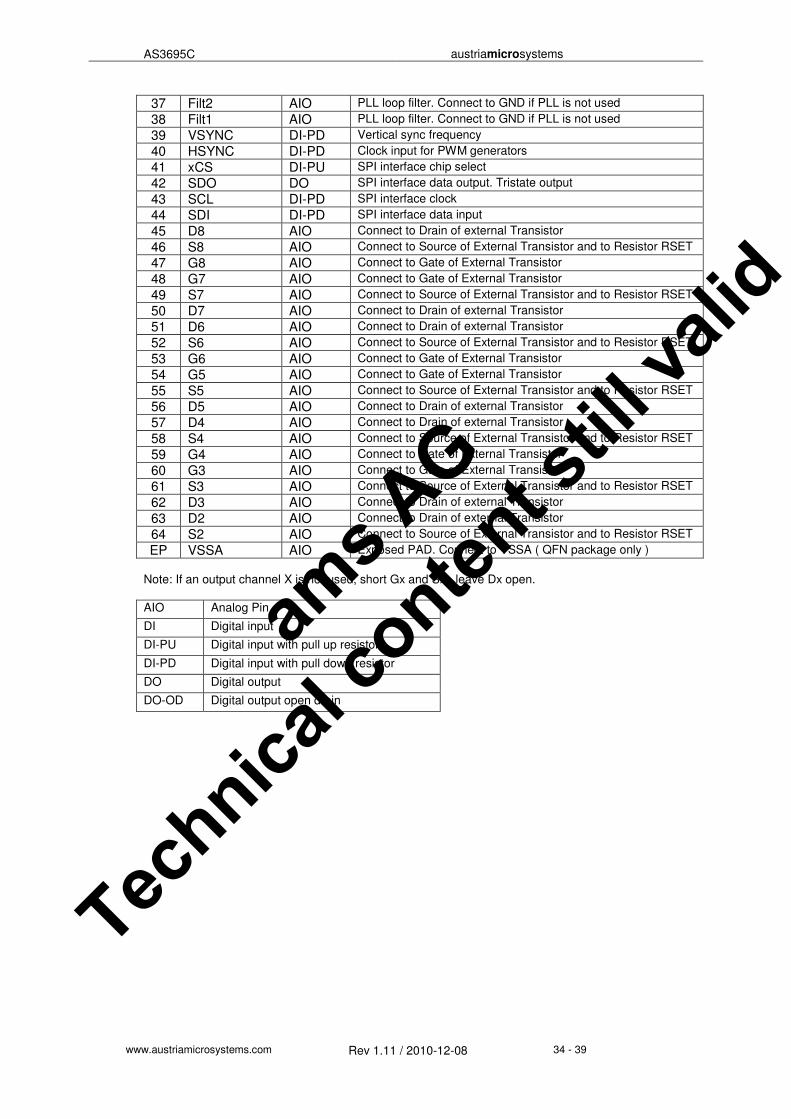
7 Pinout
Pin Nr
Pin Name
Pin Type
Description
1 G2 AIO Connect to Gate of External Transistor
2 G1 AIO Connect to Gate of External Transistor
3 S1 AIO Connect to Source of External Transistor and to Resistor RSET
4 D1 AIO Connect to Drain of external Transistor
5 V2_5 AIO Digital supply output. Connect 2.2uF bypass capacitor to GND
6 xFAULT DO- OD Fault output. Open drain. Connect pullup to VDD
7 xRES DI Reset input active low
8 FB1 AIO Power supply feedback output1
9 FB2 AIO Power supply feedback output2
10 VSSA AIO GND
11 VDD AIO Power supply. Connect 4.7uF bypass capacitor to GND
12 VSS_SENSE AIO VSS sense input. Keep this node noise free
13 D16 AIO Connect to Drain of external Transistor
14 S16 AIO Connect to Source of External Transistor and to Resistor RSET
15 G16 AIO Connect to Gate of External Transistor
16 G15 AIO Connect to Gate of External Transistor
17 S15 AIO Connect to Source of External Transistor and to Resistor RSET
18 D15 AIO Connect to Drain of external Transistor
19 D14 AIO Connect to Drain of external Transistor
20 S14 AIO Connect to Source of External Transistor and to Resistor RSET
21 G14 AIO Connect to Gate of External Transistor
22 G13 AIO Connect to Gate of External Transistor
23 S13 AIO Connect to Source of External Transistor and to Resistor RSET
24 D13 AIO Connect to Drain of external Transistor
25 D12 AIO Connect to Drain of external Transistor
26 S12 AIO Connect to Source of External Transistor and to Resistor RSET
27 G12 AIO Connect to Gate of External Transistor
28 G11 AIO Connect to Gate of External Transistor
29 S11 AIO Connect to Source of External Transistor and to Resistor RSET
30 D11 AIO Connect to Drain of external Transistor
31 D10 AIO Connect to Drain of external Transistor
32 S10 AIO Connect to Source of External Transistor and to Resistor RSET
33 G10 AIO Connect to Gate of External Transistor
34 G9 AIO Connect to Gate of External Transistor
35 S9 AIO Connect to Source of External Transistor and to Resistor RSET
36 D9 AIO Connect to Drain of external Transistor
ams A
G
Technica
l conten
t still
valid
AS3695C austriamicrosystems
www.austriamicrosystems.com Rev 1.11 / 2010-12-08 34 - 39
37 Filt2 AIO PLL loop filter. Connect to GND if PLL is not used
38 Filt1 AIO PLL loop filter. Connect to GND if PLL is not used
39 VSYNC DI-PD Vertical sync frequency
40 HSYNC DI-PD Clock input for PWM generators
41 xCS DI-PU SPI interface chip select
42 SDO DO SPI interface data output. Tristate output
43 SCL DI-PD SPI interface clock
44 SDI DI-PD SPI interface data input
45 D8 AIO Connect to Drain of external Transistor
46 S8 AIO Connect to Source of External Transistor and to Resistor RSET
47 G8 AIO Connect to Gate of External Transistor
48 G7 AIO Connect to Gate of External Transistor
49 S7 AIO Connect to Source of External Transistor and to Resistor RSET
50 D7 AIO Connect to Drain of external Transistor
51 D6 AIO Connect to Drain of external Transistor
52 S6 AIO Connect to Source of External Transistor and to Resistor RSET
53 G6 AIO Connect to Gate of External Transistor
54 G5 AIO Connect to Gate of External Transistor
55 S5 AIO Connect to Source of External Transistor and to Resistor RSET
56 D5 AIO Connect to Drain of external Transistor
57 D4 AIO Connect to Drain of external Transistor
58 S4 AIO Connect to Source of External Transistor and to Resistor RSET
59 G4 AIO Connect to Gate of External Transistor
60 G3 AIO Connect to Gate of External Transistor
61 S3 AIO Connect to Source of External Transistor and to Resistor RSET
62 D3 AIO Connect to Drain of external Transistor
63 D2 AIO Connect to Drain of external Transistor
64 S2 AIO Connect to Source of External Transistor and to Resistor RSET
EP VSSA AIO Exposed PAD. Connect to VSSA ( QFN package only )
Note: If an output channel X is not used, short Gx and Sx, leave Dx open.
AIO Analog Pin
DI Digital input
DI-PU Digital input with pull up resistor
DI-PD Digital input with pull down resistor
DO Digital output
DO-OD Digital output open drain
ams A
G
Technica
l conten
t still
valid

AS3695C austriamicrosystems
www.austriamicrosystems.com Rev 1.11 / 2010-12-08 35 - 39
8 Package drawings and Markings
Marking
Packaging code
YY WW I ZZ
Last two digits of the current year Manufacturing week Plant identifier Letters for free choice
AS3695CYYWWIZZ
ams A
G
Technica
l conten
t still
valid

AS3695C austriamicrosystems
www.austriamicrosystems.com Rev 1.11 / 2010-12-08 36 - 39
8.1 Package Drawing QFN64
ams A
G
Technica
l conten
t still
valid

AS3695C austriamicrosystems
www.austriamicrosystems.com Rev 1.11 / 2010-12-08 37 - 39
8.2 Package Drawing LQFP64
ams A
G
Technica
l conten
t still
valid

AS3695C austriamicrosystems
www.austriamicrosystems.com Rev 1.11 / 2010-12-08 38 - 39
9 Thermal characteristic
The thermal characteristics of the devices were measured at 25°C ambient temperature. The device was mounted on a double sided FR4 PCB with the bottom layer used as cooling area.
9.1 QFN64
10 Ordering information
Part Number Marking Package Type Delivery Form Description
AS3695C-ZMFT AS3695C QFN64 Tape and Reel in Dry Pack
Package size = 9x9mm, Pitch = 0.5mm, Pb-free;
AS3695C-ZLQT AS3695C LQFP64 Tape and Reel in Dry Pack
Package size = 14x14mm, Pitch = 0.8mm, Pb-free;
Bottom Layer
PCB FR4, 1cm distance from ground
Thermal vias 0.3mm
20
30
40
50
60
70
80
90
100
0 0,5 1 1,5 2 2,5 3
Tca
se
power dissipation
Tcase vs Power QFN64 with different copper area. Tamb = 25°C
0x0mm
10x10mm
20x20mm
30x30mm
50x50mm
70x70mm
0
10
20
30
40
50
60
70
80
0 10 20 30 40 50 60
Rth
_C
A [K
/W]
Area [mm^2]
Rth_CA [K/W] vs Copper Area
ams A
G
Technica
l conten
t still
valid
AS3695C austriamicrosystems
www.austriamicrosystems.com Rev 1.11 / 2010-12-08 39 - 39
Copyright Copyright © 1997-2009, austriamicrosystems AG, Schloss Premstaetten, 8141 Unterpremstaetten, Austria-Europe. Trademarks Registered ®. All rights reserved. The material herein may not be reproduced, adapted, merged, translated, stored, or used without the prior written consent of the copyright owner. All products and companies mentioned are trademarks or registered trademarks of their respective companies. Disclaimer Devices sold by austriamicrosystems AG are covered by the warranty and patent indemnification provisions appearing in its Term of Sale. austriamicrosystems AG makes no warranty, express, statutory, implied, or by description regarding the information set forth herein or regarding the freedom of the described devices from patent infringement. Austriamicrosystems AG reserves the right to change specifications and prices at any time and without notice. Therefore, prior to designing this product into a system, it is necessary to check with austriamicrosystems AG for current information. This product is intended for use in normal commercial applications. Applications requiring extended temperature range, unusual environmental requirements, or high reliability applications, such as military, medical life-support or life-sustaining equipment are specifically not recommended without additional processing by austriamicrosystems AG for each application. For shipments of less than 100 parts the manufacturing flow might show deviations from the standard production flow, such as test flow or test location. The information furnished here by austriamicrosystems AG is believed to be correct and accurate. However, austriamicrosystems AG shall not be liable to recipient or any third party for any damages, including but not limited to personal injury, property damage, loss of profits, loss of use, interruption of business or indirect, special, incidental or consequential damages, of any kind, in connection with or arising out of the furnishing, performance or use of the technical data herein. No obligation or liability to recipient or any third party shall arise or flow out of austriamicrosystems AG rendering of technical or other services.
Contact Information Headquarters austriamicrosystems AG A-8141 Schloss Premstätten, Austria T. +43 (0) 3136 500 0 F. +43 (0) 3136 5692 For Sales Offices, Distributors and Representatives, please visit: http://www.austriamicrosystems.com/contact
ams A
G
Technica
l conten
t still
valid