ashok srivastava, professor - École polytechnique...
TRANSCRIPT
Carbon Carbon NanotubeNanotube –– FET and Interconnect Modeling FET and Interconnect Modeling for Design and Analysis of for Design and Analysis of
Emerging Emerging NanoscaleNanoscale Integrated CircuitsIntegrated Circuits
Ashok Srivastava, ProfessorEmail: [email protected]
Department of Electrical and Computer EngineeringLOUISIANA STATE UNIVERSITY
Baton Rouge, Louisiana 70803, U.S.A.
Electrical Engineering Summer Research Institute (EE SRI) 2011 Ecole Polytechnique Fédérale de Lausanne (EPFL), Switzerland
17 June 2011
1

Outline of PresentationOutline of PresentationCNT FET Modeling• Motivation• Introduction to CNTs and
CNT-FETs• Electronic Structure• Current Transport Modeling• Logic Gates and Transfer
Characteristics• CNT-FET Dynamic Model• CNT-FET Small Signal
Model• CNT-FET Circuit
Simulations• Conclusion
CNT Interconnect Modeling
• CNT Interconnects for VLSI- SWCNT Interconnection Model - MWCNT Interconnection Model - SWCNT Bundle Interconnection Model
• Summary• Scope of Future Work• Selected Publications (Recent)• Acknowledgments
2

MotivationMotivation• Emerging logic devices for possible replacement of
current CMOS logic devices (after the end of Moore’s Law ~2020)
• Hybrid CMOS/Nanoelectronic digital circuits (post- CMOS nanoelectronics)
• VLSI interconnection • Hybrid semiconductor/nanowire/molecular integrated
circuits (in terabit scale memories)• Bio- and chemical sensing applications – significant
changes in CNT electronic properties when subjected to molecular adsorbates– Known hazardous gases (NH3 and NO2 )– Detection of DNA: detection of infectious agents
and drug delivery 3

Motivation
4

Carbon Nanotubes SEM micrographs of carbon nanotube bundles grown from an array of 5 mm diameter dots of iron catalyst, with various edge-to-edge spacings
The bundles shown in (a) - (d) are of 2 µm, 5 µm, 10 µm, and 20 µm edge-to- edge spacing, respectively. The inset of (a) shows a close-up of one nanotube bundle in which the individual nanotubes are visible. These micrographs show the degree of stiffness of CNT bundles as the inter-bundle spacing increases.
5
Ref.: CNT Growth (Experimental) Michael J. Bronikowski et al., JPL/Caltech “High current field emitters based on arrays of CNT bundles,” Manuscript or publication in JVST-B, Personal Communication, 2004.
Introduction Introduction –– CNT and CNTCNT and CNT--FETsFETs
• Depending on the chiral vector, carbon nanotube (CNT) can be metallic or semiconducting.
• Semiconducting CNT is one of the promising materials for the next generation of nanoscale field-effect transistors.
• Compared with the metal wires as interconnects such as the Cu, metallic CNT has distinct advantages: current densities two order of magnitude higher (~ 1010 A/cm2) and mean free path of an electron ~ several micrometers (40 nm in Cu).
• CNT wire and CNT-FET exhibit significant changes in their electronic properties (electrical resistance, thermoelectric power and density of states) when subjected to molecular adsorbates.
• CNT devices are very useful for bio- and chemical sensing applications .
• Nanotubes can be manipulated in a controlled way. There is a way of changing a nanotube's position, shape and orientation; this is possible with the use of Atomic Force Microscope.
6

Mechanical Properties of Carbon Nanotubes and Comparison with Other Materials
7
MaterialYoung's Modulus
(TPa)
Tensile Strength
(GPa)
Elongation at Break (%)
Thermal Conductivity
(W/Km)
SWCNT 1-5 13-53 16 3,500-6,600
MWCNT 0.27-0.95 11-150 8.04-10.46 3000Stainless
steel0.186- 0.214 0.38–1.55 15-50 16
Kevlar 0.06–0.18 3.6–3.8 ~2 ~1
Copper 0.11–0.128 0.22 385
Silicon 0.185 7 149

Electrical Properties of Carbon Nanotubes and Comparison with Other Materials (P. L. McEuen, M. S. Fuhrer, and H. Park, "Single-walled carbon nanotube electronics," IEEE Transactions on Nanotechnology, vol. 1, no. 1, pp. 78-85, March 2002; A. Y. Kasumov, I. I. Khodos, P. M. Ajayan, and C. Colliex, "Electrical resistance of a single carbon nanotube," Europhysics Letters, vol. 34, no. 6, pp. 429-434, 20 May 1996)
8
Semiconductor Metal
ParameterSemiconducting
SWCNT Silicon GaAs Ge Parameter Metallic SWCNT Copper
Bandgap (eV) 0.9/diameter 1.12 1.424 0.66
Mean Free Path (nm) 1,000 40
Electron Mobility (cm2/Vs)
20,000 1,500 8,500 3,900Current density
(A/cm2) 1010 106
Electron Phonon
Mean Free Path (Å)
~700 76 58 105Resistivity
(Ωm) ~10-5 1.68×10⁻⁸

Structure of Carbon Nanotubes A graphene sheet rolled in a tubular form
• Two basic types of carbon nanotubes: single-walled nanotubes (SWCNTs) and multi-walled nanotubes (MWCNTs). A SWCNT can be described as a graphene sheet rolled into a cylindrical shape so that the structure is one dimensional with axial symmetry, and in general exhibiting a spiral conformation, called chirality.
9

Chiral Vector: Properties of a CNT are predicted by the indices (n,m) inscribed in the Chiral Vector
• a1 and a2 are the graphene lattice vectors and n and m are integers which represent the number of hexagons along the directions of a1 and a2 , respectively.
• If (n-m) is zero or multiple of 3, the CNT is a metal, for all other combinations the CNT is a semiconductor.
It is possible to describe the electronic structure and density of states as a function of the chiral vector.
10
),(21 mnamanCh
yxaayxaa ˆˆ32
and ˆˆ32 21

Carbon Nanotube
11

Band Gap of a Carbon Nanotube
All Carbon nanotubes do not have the same band gap, because for every circumference there is a unique set of allowed valence and conduction states.
The smallest-diameter nanotubes have very few states that are spaced far apart in energy.
As nanotube diameters increase, more and more states are allowed and the spacing between them shrinks.
In this way, different-size nanotubes can have band gaps as low as zero (like a metal), as high as the band gap of silicon, and almost anywhere in between. No other known material can be so easily adjusted. Energy gap can be varied continuously from from 0 eV to 1 eV, by varying the nanotube diameter. 12

The Future of Microelectronics• Although the development of Silicon Based Microelectronics over the past decade has been
outstanding, nothing can be kept going forever. Many scientists expect that within a few years; a number of factors, such as fabrication limitations and economic factors, will halt the miniaturization of silicon devices.
• Further microelectronics developments would then be required, the use of different materials, different fabrication principles, and different device concepts will be needed. Carbon Nanotubes Transistors (non-classical devices) are among one of the next steps in microelectronics research.
• Use in Digital Electronics: Stanford Report, December 8, 2009: New Stanford techniques make carbon-based integrated circuits more practical (Multi-stage digital logic circuits using carbon nanotube FETs, IEDM Tech. Digest, 2009).
• Use in Analog Electronics: SWCNT Power Amplifiers for VHF range ( power gains of 1-14 dB up to 125 MHz and SWCNT transistor radios (Kocabas et al., “Radio frequency analog electronics based on carbon nanotube transistors,” PNAS, Feb 5, 2008, vol. 5, no. 5, pp. 1405-1409).
• CNT-FETs (p-type, back-gated) with intrinsic cut-off frequencies up to 80 GHz have been demonstrated [Le Louarn et al., APL, vol. 90, 233108 (2007), L = 300 nm and W = 10 μm ; Nougaret et al., APL, vol. 94, 243505 (2009), L = 300 nm and 20 μm (10 μm/gate)].
• According to some benchmarking studies, CNT has the potential to provide high- performance p-FETs RF technology complementing silicon and III-Vs in heterogeneously integrated systems.
13
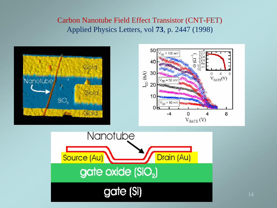
Carbon Nanotube Field Effect Transistor (CNT-FET)Applied Physics Letters, vol 73, p. 2447 (1998)
14

This is the basic model for a CNFET, as it can be seen the carbon nanotube is placed in the location where the channel would normally form in a MOSFET.
Carbon Nanotube Field Effect Transistor (CNT-FET)
15
Carbon Nanotube Field Effect Transistors (CNT-FETs)
• A CNT-FET achieves an operation similar to a MOSFET using a SWCNT as the conductive channel.
• The conductance of a SWCNT varies depending on the terminal voltages. This dependence is used to control the current by varying the conductance of the SWCNT through the gate voltage.
16

Carbon Nanotube Field Effect Transistors (CNT-FETs)
• First CNT-FET was fabricated in 1998 by Dekker’s Group (“Room temperature transistor based on a single carbon nanotube,” Nature, vol. 393, pp. 49-52, May 1998). These transistors were back gate geometry type.
• Major improvement was seen in 2002 with the use of top gate geometry. Transconductances of ~3.25µS were achieved (compared to ~0.3 µS from back gate geometry).
• In 2003, improved electrode materials eliminated the Schottky barrier at the drain and source of CNT-FETs (Javey et al., “Advancement in complementary carbon nanotube field-effect transistors,” IEDM Technical Digest, Dec. 2003)
• In 2004, CNT-FETs with small or no Schottky barrier at the electrode - CNT interface were implemented.
17

Cross-section of a CNT-FET
The structure is very similar to that of a typical MOSFET, except for an additional oxide layer on top of the substrate. In addition, the source and drain are replaced with electrodes.
18

p-type and n-type CNT-FETsp-type CNT
• When CNT-FETs were first fabricated in 1998, they showed typical I-V characteristics of a p-type semiconductor implying a p-type CNT.
• P-type behavior was due to the absorption of oxygen during the fabrication process.
• However, it was found that the role of oxygen was not to dope the CNT, but to change the work function of a portion of the metal electrode at the electrode- CNT interface favoring the conduction of holes.
n-type CNT• Derycke et al., fabricated n-type CNT-FETs by annealing in vacuum
(suppressing the oxygen) and using conventional doping with an electron donor such as potassium.
• As a result, n-type CNT-FETs are achieved by controlling the oxygen exposure or by conventional doping.
• Oxygen basically shifts the energy levels at the drain/source contacts by gradually decreasing the electron conduction.
In essence, it can be suggested that the use of oxygen-exposure is to manipulate the Schottky barriers and of conventional doping to shift the threshold voltage.19

Electronic StructureElectronic Structure
• Energy dispersion relation of a SWCNT– Calculated from the 2D-Energy Dispersion
relation of graphene.– Using the reciprocal wave vectors of SWCNTs,
1D-Energy Dispersion relation is mapped from that of graphene and is given by:
2/1
21 2
422
341)(
a
KCosa
KCosaKCosVkE yyx
ppD
20

Electronic Structure
Energy band diagram in k-space for a CNT with (a) chiral vector (4,2) and (b) chiral vector (8,2). Here, Vppπ
= 2.7eV.

Density of States
Plot of the density of states using numerical techniquesfor a CNT with a chiral vector (4,3)
22
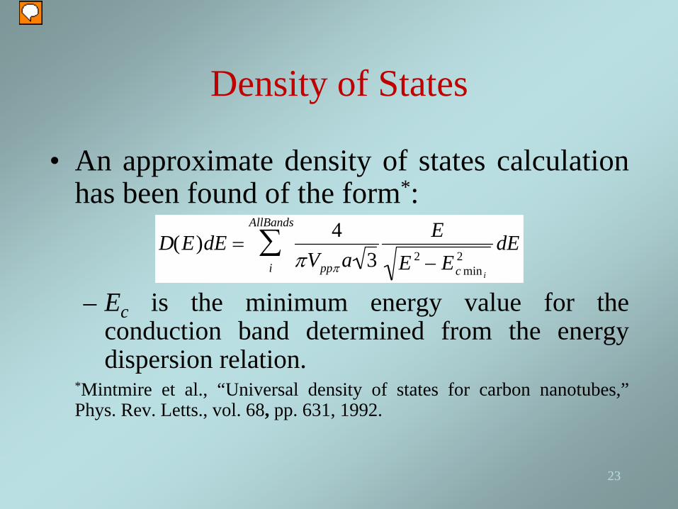
Density of States
• An approximate density of states calculation has been found of the form*:
– Ec is the minimum energy value for the conduction band determined from the energy dispersion relation.
*Mintmire et al., “Universal density of states for carbon nanotubes,” Phys. Rev. Letts., vol. 68, pp. 631, 1992.
D(E)dE 4
Vppa 3E
E 2 Ec min i
2dE
i
AllBands
23

Effective Mass
• Given the complete energy dispersion relation of CNTs, the electron mass can be calculated from the following semiconductor effective mass relationship expression:
2
2
2*
dkEd
mi
24

Effective Mass(n,m) Effective mass of electrons (m*)
(3,1) 0.507 m0†
(3,2) 0.222 m0
(4,2) 0.271 m0
(4,3) 0.175 m0
(5,0) 0.408 m0
(5,1) 0.159 m0
(5,3) 0.189 m0
(6,1) 0.255 m0
(7,3) 0.116 m0
(9,2) 0.099 m0
(11,3) 0.108 m0
†m0 is the mass of an electron (9.109 x 10⁻³¹Kg) 25

Carrier Concentration
• The carrier concentration in a semiconductor is given by:
– D(E) is the density of states, f(E) is the Fermi function and Ec is the conduction band energy minimum.
cE
cnt dEEfEDn )()(
26

Carrier Concentration
• Using the approximate density of states:
We can further simplify this equation by replacing variable E with E+Ec and letting
and .The summation can be dropped since the Fermi function becomes negligible for bands beyond the first one.
AllBands
i E
kTEE
cpp
cnt
ic
F
idEeEEE
aVn
12/122 1
34
x EkT EF Ec
kT
27

Carrier Concentration
Defining and we can write:
where
An analytical solution can be found by using the limits: and
0
12/1 123
4 dxeExkTxExkTaVkTn x
ccpp
cnt
G x kTx Ec x1 2 kTx 2Ec 1 2 F x 1
1 ex
00 111 dx
exG
kTNdxxFxG
kTNn xcccnt
Nc 4kT
Vppa 3
1 1
28

Intrinsic Carrier Concentration(n,m) Intrinsic carrier concentration (cm-3)
(3,2) 7.042 x 10⁴
(4,2) 6.303 x 10⁶
(4,3) 1.239 x 10⁹
(5,0) 2.401 x 10⁵
(5,1) 2.677 x 10⁸
(5,3) 1.791 x 10¹⁰
(6,1) 1.656 x 10⁹
(7,3) 5.238 x 10¹²
(9,2) 4.911 x 10¹³
(11,3) 6.034 x 10¹⁴
Note the similarity in concentration of chiral vector (5,3) and that of silicon (1.5 x 10¹⁰). 29

Temperature Dependence
Plot of the intrinsic carrier dependence on temperature for a carbon nanotube with chiral vectors (4,2), (4,3) and (7,3)
30

Temperature Dependence
Plot of the carrier concentration dependence on temperature for a carbon nanotube with chiral vector (4,3) and a doping
concentration of 1015 donor atoms. 31

Energy Separation (EC - EF )
Plot of the energy separation (EC - EF ) versus doping concentration fortwo carbon nantoubes with chiral vectors (4,2) and (10,0)
32

Current Transport ModelingCurrent Transport Modeling
• The charge inside the carbon nanotube can be obtained from the electronic structure and carrier concentration.
• A model for the carbon nanotube potential in terms of the terminal voltages can be derived.
• Using these results a current equation can then be established.
33

Charge and Potential Distributions
Plot of the charges from gate to substrate and plot of thepotential distribution from gate to substrate in a CNT-FET
34

Energy Band Diagram of a Two Terminal CNT-FET for (a) Vgb = Vfb and (b) Vgb > 0
35
(a)
EVAC
EC
EFMEC
EC
EV
EV
EV
Aluminium HfO2 SiO2 p+ - SubstrateCNT
EC
EV
qcnt,s=q0
qVgb = qVfb
EVAC
q0
(b)
EVAC EC
EFM
EC
EC
EV
EVEV
Aluminium HfO2 SiO2 p+ - SubstrateCNT
EC
EV
EVAC
qVgb
qcnt,s
qVcb
EF
EFsurf
EFsurf - ECsurf = EF - qVcb+cnt,s - q0 - EC
ECsurf
Ref.: A. Srivastava, J. Marulanda, Y. Xu and A. K. Sharma, “Current transport modeling of carbon nanotube field effect transistors,” physica status solidi (a), vol. 206, no. 7, pp. 1569-1578, 2009.

Gate Voltage Equation• From the charge neutrality and potential
balance conditions we can write:
Using Maxwell third equation we arrive at:
• subs and ox1 are the permittivity constants of substrate and oxide regions, respectively.
Vgb ms ox1 cnt ox 2 subs
Q'g Q'01Q'02 Q'cnt Q'subs 0
cntsubsoxoxsubssubs QQQQEE '''' 020111
36

Gate Voltage Equation• Tox2 is much greater than Tox1 .• Deep in the substrate, the electric field is
negligible.• Esubs and ψsubs can be neglected:
where for a CNT of length, L and radius, r the oxide capacitance is given by
2102
1
01
1 '1
'1''
''
''
oxoxsubs
oxms
ox
cntcntgb CC
QQCQ
CQV
rrTTrT
LC
oxoxox
oxox
2ln
22
37

Charge Inside the CNT
• Using the carrier concentration and the relation we have:
• Limit 1
• Limit 2
cntnLqnQ cntcnt
kTEE
ccnt
cF
eINQ
kTEE
NQ cFccnt
22
1
1
38

Carbon Nanotube Potential
• The Fermi level can be written as
where Vcb is the channel potential and varies from the source voltage, Vs to the drain voltage, Vd .
cbcntF VqE
2102
1
01
1 '1
'1''
''
''
oxoxsubs
oxms
ox
cntcntgb CC
QQCQ
CQV
39

Carbon Nanotube Potential
• The gate to substrate voltage is then given by:
where
and
This expression cannot be solved for ψcnt .
fbcbcntcntgb VVFV ,
qkT
qE
cbcntcF
qkT
qE
cbcntkT
EVq
cbcntc
cccbcnt
VforkT
EE
VforeVF
;
; , 22
2102
1
01
'1
'1''
''
oxoxsubs
oxmsfb CC
QQCQV
1ox
c
CIqLN
,
40

Carbon Nanotube Potential
Carbon nanotube potential versus gate substrate voltage for a CNT-FET(7,2)
41

The Current Equation
• Both diffusion and drift mechanism contribute to the current.
• The mobility can be found from that of graphite using where is a conversion factor since the mobility will change depending on the chiral vector (n,m).
graphiteeff
42
cnt
L
cntcnt
LQ
Qdriftdiffds dQdQ
qkT
LR
xIxIIcnt
cnt
cnt
cnt
00
''2

Static Model
*A. Srivastava, J. M. Marulanda, Y. Xu and A. K. Sharma, "Current transport modeling of carbon nanotube field effect transistors," physica status solidi (a), vol. 206, no. 7, pp. 1569-1578, 2009.
Current equations* are given as follows, which include drift current and diffusion current.
gsscntdiffgsscntdiff
gsscntdriftgsscntdrift
diffdriftds
VfVLf
VfVLf
III
,0,
,0,
,,
,,
21
,,
2,,,
,
21,
LC
scntgsscntdiff
scntscntfbsbgsgsscntdrift
ox
xq
kTVxf
xxVVVVxf
The parameters are defined as follows: L: gate length, μ: carrier mobility, k: Boltzmann constant, : conversion factor to account for the mobility change with the chiral vector (n,m). T: temperature, oK, Vfb : flat-band voltage, Vsb : source-substrate voltage and Cox1 : gate-oxide capacitance per unit area.
where
The Current Equation: CNT-FET Model

Current Equation
• Depending on which Region is used for ψcnt (L), two regions of operation for the current can be defined.– Linear Region
• ψcnt (L) is almost independent of Vgs .
– Saturation Region • ψcnt (L) is linearly dependent on Vgs .
SlopeqkT
qE
fbgsdsIeVVV c 1
SlopeqkT
qE
fbgsdsIeVVV c 1
44

I-V Characteristics
I-V characteristics using Q01 = Q02 = 0, Tox1 = 15 nm,Tox2 = 120 nm and L = 260 nm for a CNT-FET(3,1).
Experimental data (o): Ref.: Wind et al., "Vertical scaling of carbon nanotube field-effect transistors using top gate electrodes," Applied Physics Letters, vol. 80, pp. 3817-3819, 2002. 45

As considered in MOSFET, a channel length modulation parameter, is also introduced in our CNT-FET model. In the saturation region, current transport equation is modified as follows:
dsgsscntgsscntds VVfVLfI 1,0, ,,
The Current Equation: CNT-FET Model Static Model

CNT-FET I-V Characteristics
I-V characteristics of CNT-FET (11,9) and Current, Ids versus gate to source voltage, Vgs , with Vfb = -0.79 V and ф0 = 0. The device dimensions are Tox1 =15 nm, Tox2 =120 nm and L=250 nm. In modeled curve, Q01 =Q02 =0 and =0.1 V-1. Experimental data (o): Ref.: Wind et al., "Vertical scaling of carbon nanotube field-effect transistors using top gate electrodes," Applied Physics Letters, vol. 80, pp. 3817-3819, 2002.
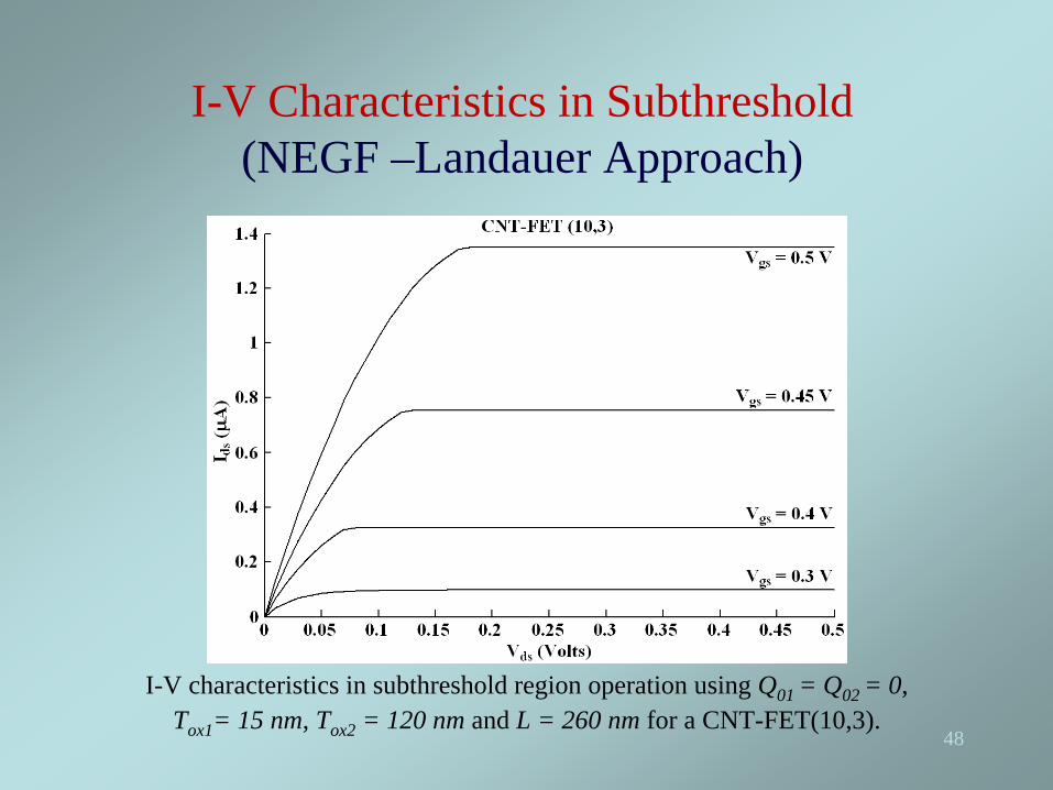
I-V Characteristics in Subthreshold (NEGF –Landauer Approach)
I-V characteristics in subthreshold region operation using Q01 = Q02 = 0,Tox1 = 15 nm, Tox2 = 120 nm and L = 260 nm for a CNT-FET(10,3).
48

Threshold Voltage Modeling
• Charge inside the carbon nanotube versus the gate voltage can be plotted from:– the expression for the charge in terms of the
Fermi levels and using numerical techniques to find the CNT potential.
– the gate voltage equation solved for the charge and using analytical equations for the carbon nanotube potential.
49

Charge versus Gate Voltage
CNT charge, Qcnt versus gate voltage, Vgs , for a CNT-FET(7,2) using L = 50 nm, Tox1 = 40 nm and Tox2 = 400 nm.
50
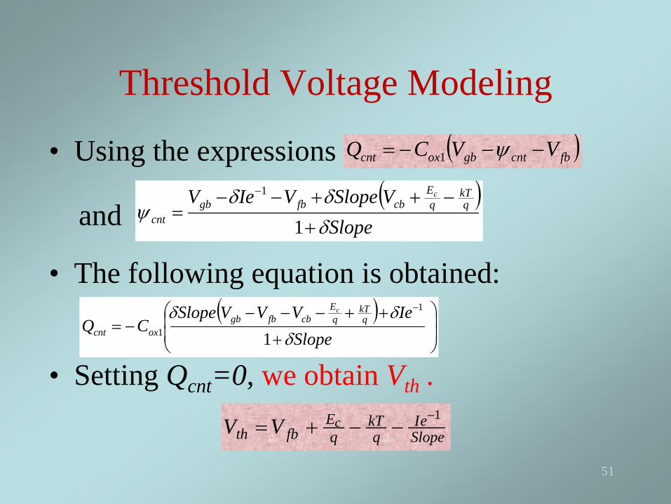
• Using the expressions
and
• The following equation is obtained:
• Setting Qcnt =0, we obtain Vth .
Slope
VSlopeVIeV qkT
qE
cbfbgbcnt
c
1
1
Threshold Voltage Modeling fbcntgboxcnt VVCQ 1
SlopeeI
qkT
qE
fbthcVV
1
SlopeIeVVVSlope
CQ qkT
qE
cbfbgboxcnt
c
1
1
1
51

Saturation Voltage Modeling
• Using a numerical and an analytical approach to find the CNT potential.
• Charge inside the carbon nanotube versus the channel potential can be plotted in a similar manner as it was done for the threshold voltage derivation.
52

Charge versus Channel Voltage
CNT charge, Qcnt versus channel to bulk voltage, Vgs , for aCNT-FET(7,2) using L = 50 nm, Tox1 = 40 nm and Tox2 = 400 nm.
Note: Solid line – numerical, dotted line – analytical 53

Saturation Voltage Modeling
• Using the equation
• Setting Qcnt =0 and Vcb =Vds,sat and solving for Vds,sat , we obtain:
SlopeeI
qkT
qE
fbgssatdscVVV
1,
SlopeIeVVVSlope
CQ qkT
qE
cbfbgboxcnt
c
1
1
1
54

Results for Vth and Vds,sat
CNT-FET (n,m) Vth (V)Vds,sat (V)
Vgs = 1.5 V Vgs = 2 V
(3,1) 0.469 1.031 1.531
(3,2) 0.154 1.346 1.846
(4,2) 0.040 1.460 1.960
(4,3) -0.107 1.607 2.107
(5,0) 0.143 1.357 1.857
(5,1) -0.066 1.566 2.066
(5,3) -0.176 1.676 2.176
(6,1) -0.105 1.605 2.105
(7,3) -0.333 1.833 2.333
(9,2) -0.393 1.893 2.393
(11,3) -0.462 1.962 2.462
55

Voltage Transfer Characteristics of Voltage Transfer Characteristics of Logic GatesLogic Gates
• Although the analytical current model was based on an n-type CNT-FET, the same principle can be applied to a p-type CNT- FET, with the respective polarity changes.
• However, the equations remain the same.• Complementary logic gates can be modeled
and described.
56

Logic Gates
CNT-FET logic: (a) Inverter, (b) two input NAND gate and (c) two input NOR gate.
57

CNT-FET logic: (a) Inverter, (b) two input NAND gate and (c) two input NOR gate
Logic Gates ModelingNon-Ballistic CNT-FET Model
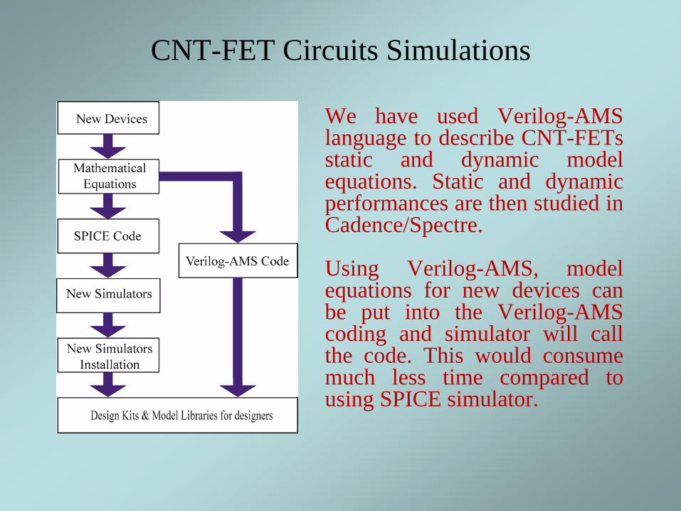
CNT-FET Circuits Simulations
We have used Verilog-AMS language to describe CNT-FETs static and dynamic model equations. Static and dynamic performances are then studied in Cadence/Spectre.
Using Verilog-AMS, model equations for new devices can be put into the Verilog-AMS coding and simulator will call the code. This would consume much less time compared to using SPICE simulator.

Voltage transfer characteristics of an inverter using CNT-FETs (11,9) with Vfb = 0 V,
= 0, 0.1 V-1 and ф0 = 0. The dimensions of both the n-type CNT-FET and p-type CNT- FET are: Tox1 = 15 nm, Tox2 = 120 nm and L = 250 nm. Experimental: Ref. Derycke, V. et al., Nano Lett., vol. 1, 453 (2001).
Logic Gates ModelingNon-Ballistic CNT-FET Model

Voltage transfer characteristics of (a) an inverter and a NAND gate (b) an inverter and a NOR gate using CNT-FETs (11,9) with Vfb = 0 V and ф0 = 0. The dimensions of both the n-type CNT-FET and p-type CNT-FET are: Tox1 = 15 nm, Tox2 = 120 nm and L = 250 nm.
Logic Gates ModelingNon-Ballistic CNT-FET Model

Voltage Transfer Characteristics of Logic Gates
• Transfer characteristics show similar behavior as typical CMOS gates.
• The CNT based inverter shows a sharp transition at 1.0V for 2V operation.
• The CNT based NAND and NOR gates also show a sharp transition for 2V operation.
62

Dynamic Model
CNTCNT--FET: Dynamic ModelFET: Dynamic Model
Meyer capacitance model. Ref: Y. Cheng and C. Hu, MOSFET Modeling and BSIM3 User’s Guide, Springer, 1999.

Capacitances of CNT-FET (11,9) with Vfb = -0.79 V and Ф0 = 0. The device dimensions are Tox1 =15 nm, Tox2 =120
nm and L=250 nm.
Physically, Cgb is negligible since Qcnt shields the gate from the bulk and prevents any response of the gate charge to a change in the substrate bias. If we consider the small change of Qsubs , Cgb will be a very small value compared with Cgs and Cgd .
In the saturation region, the channel is pinched- off at the drain end of the CNT-FET. This electrically isolates the CNT from the drain so that the charge on the gate is not influenced by a change in the drain voltage and Cgd vanishes. The results are in same order with calculated results by Deng and Wong*.
*J. Deng and H. S. P. Wong, "A compact SPICE model for carbon-nanotube field- effect transistors including nonidealities and its application-Part I: model of the intrinsic channel region," IEEE Transactions on Electron Devices, vol. 54, no. 12, pp. 3186-3194, December 2007.
Dynamic ModelCNT-FET Model

Definition of capacitances Cgb , Cgs and Cgd :
gbgsgdgbgdgs VVgd
ggd
VVgs
ggs
VVgb
ggb V
QC
VQ
CVQ
C,,,
,,
Dynamic ModelCNT-FET Model

CNTCNT--FET Model: Small Signal Equivalent FET Model: Small Signal Equivalent Circuit ModelCircuit Model
Small signal high frequency equivalent circuit model of a CNT-FET.
66

Small Signal Equivalent Circuit Model Small Signal Model Parameters
(n,m) gm (µS) Rds (KΩ) Cgs (aF)
(3,1) 111 132 0.905
(3,2) 130 155 0.920
(4,2) 142 163 0.935
(4,3) 152 174 0.946
(5,1) 148 171 0.939
(5,3) 160 179 0.958
(6,1) 157 174 0.952
(7,3) 173 190 0.978
(9,2) 181 195 0.990
(11,3) 191 200 1.011
Small Signal parameters of CNT-FETs using Q01 = Q02 = 0, Tox1 = 40 nm, Tox2 = 400 nm and L = 50 nm. 67

Small Signal Equivalent Circuit Model Cut-Off Frequency
• The cut off frequency in a CNT-FET can be calculated from the expression:
• In calculating the cut off frequency the transistor is considered to be operating in saturation.
• Values for Vgs and Vds are chosen and gm and Rds are calculated accordingly.
mcdscpardscgs
mT
gRgRCgRCgf
22121
68

Small Signal Equivalent Circuit Model Cut-Off Frequency and gm
Dependence of cut-off frequency on gm of a CNT-FET (11,3).
69

Small Signal Equivalent Circuit Model Cut-Off Frequencies versus Chiral Vectors
(n,m) CNT-FETfT (GHz)
(3,1) 539
(3,2) 615
(4,2) 656
(4,3) 689
(5,1) 674
(5,3) 716
(6,1) 704
(7,3) 755
(9,2) 779
(11,3) 807
70CNT-FETs (p-type, back-gated) with intrinsic cut-off frequencies up to 80 GHz have been demonstrated[Ref. Le Louarn et al., APL, vol. 90, 233108 (2007), L = 300 nm and W = 10 μm ; Nougaret et al., APL, vol. 94, 243505 (2009), L = 300 nm and 20 μm (10 μm/gate)].

CNT-FET Circuits Simulations – Ring Oscillator
*Z. Chen, J. Appenzeller, P. M. Solomon, Y.-M. Lin, and P. Avouris, "High performance carbon nanotube ring oscillator," Proc. 64th Device Research Conference, State College, PA, USA, pp. 171-172, June 26-28, 2006.
• Left figure (a) shows the schematic of the five-stage ring oscillator which was fabricated in the work of Chen et al.*
• Left figure (b) shows the simulation result of the ring oscillator output waveform at 0.92 V supply voltage.
• Left figure (c) shows the oscillation frequency with different supply voltage.
• Model and experiments show that the oscillating frequency of this ring oscillator is only about 70-80 MHz at 1.04 V supply voltage.
This is due to the CNT-FETs in the ring oscillator which are 600 nm long and there are parasitic capacitances associated with the metal wires in the ring oscillator.

CNT Biosensors
(a) Illustration of a single SWCNT-FET during electrical measurements(b) Single sensor chip with four SWNT-FETs.
Ref.: Tang et al., "Carbon nanotube DNA sensor and sensing mechanism," Nano Letts., vol. 6, No. 8, pp. 1632-1636, 2006.
After MCH attachment to gold electrodes, I-Vg curves are taken by a sweeping silicon back gate.72
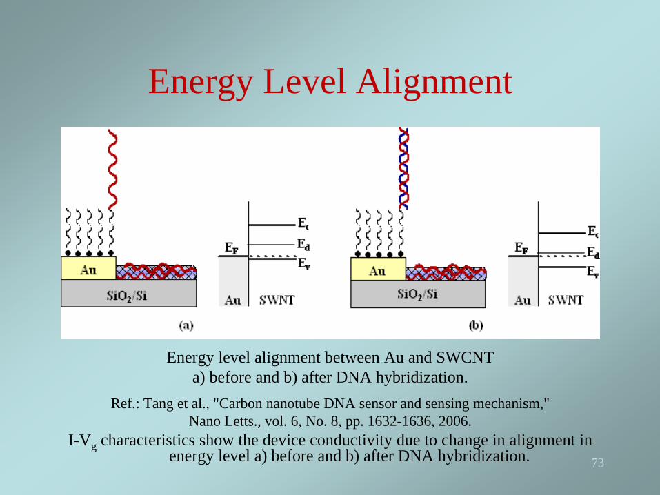
Energy Level Alignment
Energy level alignment between Au and SWCNTa) before and b) after DNA hybridization.
Ref.: Tang et al., "Carbon nanotube DNA sensor and sensing mechanism," Nano Letts., vol. 6, No. 8, pp. 1632-1636, 2006.
I-Vg characteristics show the device conductivity due to change in alignment in energy level a) before and b) after DNA hybridization. 73

ConclusionConclusion• Current transport in CNT-FET (MOSFET like geometry)
is studied analytically and model equations are obtained.• Dynamic and small-signal CNT-FET models are also
discussed.• Current transport models can be used in analysis and
design of emerging complementary CNT-based integrated circuits.
• Models can be used in Cadence/Verilog-AMS for circuit simulations.
• Current model equations can provide a much better understanding of the changes in electronic properties of CNTs and CNT-FETs when exposed to molecular adsorbates.
74

75
CNT Interconnection for VLSICNT Interconnection for VLSI• Applications of metallic Carbon
Nanotubes: interconnection wire in VLSI
High current density
Small resistance
Large mean free path than Cu
Substitute for Cu interconnects in sub- 22 nm technology nodes

CNT Interconnect Modeling for Integrated Circuit Design - Objective
• Model carbon nanotube interconnects (SWCNT, MWCNT, SWCNT bundle) and develop equivalent circuit models.
• Combine the models of CNT-FETs and CNT interconnects for designing and characterization of CNT-FET integrated circuits.
76

SWCNT Interconnection Model
•Two-dimensional electron fluid*:External electrical field drifts electrons in z direction while electrons can also distribute in perpendicular (y) direction to form a two-dimensional fluid.
•One-dimensional electron fluid**: The y direction shrinks into one point and the distributed electrons in y direction in a two-dimensional system will be at the same point in one- dimensional system. As a result, the repulsive force among the electrons will be significant. The external electric field provides both the potential and kinetic energy to the one-dimensional fluid.
potentialkinetictotal EEE
kinetictotal EE
*Maffucci, A., Miano, G. and Villone, F., "A transmission line model for metallic carbon nanotube interconnects," Int. J. Circ. Theor. Appl., vol. 36, pp. 31-51 (2008).**Y. Xu and A. Srivastava, "A model for carbon nanotube interconnects," Int. J. Circ. Theor. Appl., vol. 38, no. 6, pp. 559-575, August, 2010. Also published online in Wiley InterScience.

SWCNT Interconnection Model• One-Dimensional Fluid ModelOne-dimensional fluid model basic equation (Euler’s Equation):
where n is the electron density, v is the electron mean velocity, p is the pressure, m is the electron mass, e is the electronic charge and Ez is electric field.
The last term on the right hand side represents the effect of scattering of electrons with the positive charge background and υ is the electron relaxation frequency. The relaxation frequency, υ is related to the mean-free path, λ. The parameter α
describes the classical electron-electron repulsive interaction.
zszzz vmnenzpv
zv
tmn
E)1(

SWCNT Interconnection Model
Current transport equation for a one-dimension electron fluid in a metallic CNT:
The equation relates current density, charge density and electric field in a CNT. The density of conduction electrons is no . The third term on the left-hand side of the equation can be neglected since metallic CNT is a good conductor, we can obtain an equation for current density in frequency domain:
Continuity equation on the surface, s′ :
where σ is the charge density and n is the electron density. The current density, j=envz and vz is the electron velocity in z-direction.[Y. Xu and A. Srivastava, “A model of carbon nanotube interconnects,” Int. J. Circuit Theory and Applications, vol. 38, Issue 6, pp. 559-575, 2010. Published online: 2 March 2009 by Wiley InterScience, DOI: 10.1002/cta.587, pp. 1-17, 2009]
79
ze mne
ztzuj
ttzj E
1),(),( 02
2
0
zenv
tne
zj
tZ
E
imne
j
11ˆ 0
2

Parameter
is defined as:
PK
PP
z
zP
EEE
EE
EE
Ez and EzP are respectively, the total electrical field and the part of the electrical field which provides potential energy to electrons in z-direction. E is the total energy of electrons. EP and EK are the potential and kinetic energies of electrons, respectively.
SWCNT Interconnection Model
• One-Dimensional Fluid Model

Plasmon sound velocity:
1F
evu
The parameter
describes the ratio of Fermi velocity to the plasmon sound velocity.
SWCNT Interconnection Model
• One-Dimensional Fluid Model

SWCNT Interconnection Model
where
• Transmission Line Model
zq
CtiLRi
QKz
1E
20
2
1 ,1
12
,)sgn(eK
QKK uLC
nremLlLR

rhCE 1cosh
2
*S. Ramo, J. R. Whinnery and T. Van Duzer, Fields and Waves in Communication Electronics, New York: Wiley, 1994.
KM LrhL
1cosh
2
The magnetic inductance and electric capacitance per unit length of a perfect conductor on a ground plane*
are:
SWCNT Interconnection Model• Transmission Line Model

Zin
versus frequency for different lengths of SWCNTs. And Zin
versus frequency using different model for a 10 µm length SWCNT.
• SWCNT interconnects show resonances at lower frequencies. Resonances of 0.1 μm and 1 μm SWCNT are shown in bottom left figure as an inset.
• With increasing length, the resonance frequency range increases, thus limiting the use of SWCNT interconnects. It is observed in CNTs below close to 1 MHz, 10 MHz and 100 MHz for lengths less than 1 µm, 10 µm and 100 µm, respectively. Short lengths CNTs (< 1 µm) can be used above 1 MHz.
• However, considering the resonances range and applications, SWCNT interconnects are very promising.
SWCNT Interconnection Model• Simulation Results

Bottom figure shows the schematic of a 2-port network used in study of S- parameters. Interconnect can be Cu or SWCNT. RS is the terminating impedance. The terminating impedances of SWCNT and Cu interconnect lines used in S-parameters studies are 3.2 kΩ
and 50 Ω, respectively. In the case of SWCNT interconnect lines; the terminal impedance is equal to its contact resistance.
SWCNT Interconnection Model• Simulation Results

S21 (amplitude) versus frequency for different lengths CNT and Cu interconnects.
• The transmission efficiency of both the CNT and Cu interconnects decreases with increasing lengths.
• However, CNT transmission line has larger 3 dB bandwidth and magnitude of S21 when compared with Cu interconnects. |S21 | for both CNT and Cu interconnects approaches to 0 dB for lengths less than 1 µm.
• The 3 dB bandwidth of short CNT interconnect lengths, 0.1 μm or less could exceed 1 THz.
SWCNT Interconnection Model• Simulation Results

Group delay versus frequency for different lengths SWCNT and Cu interconnects.
• Shorter the length, lower is the delay for both SWCNT and Cu interconnects.
• SWCNT interconnects exhibit larger bandwidths but group delay larger than the same length Cu interconnects.
SWCNT Interconnection Model• Simulation Results

• In 1D fluid model, the difference in Fermi velocity and sound velocity is due to electron-electron repulsive interaction, which is a classical concept, referring to the repulsive electrostatic forces only between electrons. Therefore, the electron-electron interaction is distributed over a short range.
• In Lüttinger liquid model, the difference in Fermi velocity and plasmon sound velocity is due to electron-electron correlation, which is a quantum concept, referring to the interaction between electrons in a quantum system, the electronic structure of which is being considered. Therefore the electron-electron correlation is distributed over the length of the CNT.
• Study of S-parameters suggests consideration of impedance matching at the input and output to minimize losses due to reflections for longer CNT interconnects. The results from our modeling of CNT interconnects and comparison with Cu interconnects show the possibility of using metallic CNTs as interconnects for next generation of VLSI circuits.
SWCNT Interconnection Model• Summary

MWCNT Interconnection Model
A comparison of calculated and measured resistances of MWCNT interconnects:
References
MWCNT Physical Parameters MWCNT Resistance (kΩ)
Length (µm) D1 (nm) Dn (nm) lmfp (µm) Measured
Our Model
Nihei et al.* 2 10 3.88 <1 1.60 1.90
Li et al. # 25 100 50 >25 0.035 0.042
*M. Nihei, D. Kondo, A. Kawabata, S. Sato, H. Shioya, M. Sakaue, T. Iwai, M. Ohfuti, and Y. Awano, "Low-resistance multi-walled carbon nanotube vias with parallel channel conduction of inner shells," Proc. IEEE International Interconnect Technology Conference, San Francisco, CA, USA, pp. 234-236, June 6-8, 2005.
#H. J. Li, W. G. Lu, J. J. Li, X. D. Bai, and C. Z. Gu, "Multichannel ballistic transport in multiwall carbon nanotubes," Phys. Rev. Lett., vol. 95, no. 8, pp. 86601-1 to 86601-4, 19 August 2005.
MWCNT Interconnection Model
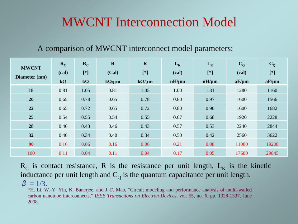
A comparison of MWCNT interconnect model parameters:
*H. Li, W.-Y. Yin, K. Banerjee, and J.-F. Mao, "Circuit modeling and performance analysis of multi-walled carbon nanotube interconnects," IEEE Transactions on Electron Devices, vol. 55, no. 6, pp. 1328-1337, June 2008.
MWCNT
Diameter (nm)
RC
(cal)
k
RC
[*]
k
R
(Cal)
k/m
R
[*]
k/m
LK
(cal)
nH/µm
LK
[*]
nH/µm
CQ
(cal)
aF/µm
CQ
[*]
aF/µm
18 0.81 1.05 0.81 1.05 1.00 1.31 1280 1160
20 0.65 0.78 0.65 0.78 0.80 0.97 1600 1566
22 0.65 0.72 0.65 0.72 0.80 0.90 1600 1682
25 0.54 0.55 0.54 0.55 0.67 0.68 1920 2228
28 0.46 0.43 0.46 0.43 0.57 0.53 2240 2844
32 0.40 0.34 0.40 0.34 0.50 0.42 2560 3622
90 0.16 0.06 0.16 0.06 0.21 0.08 11080 19208
100 0.11 0.04 0.11 0.04 0.17 0.05 17680 29845
RC is contact resistance, R is the resistance per unit length, LK is the kinetic inductance per unit length and CQ is the quantum capacitance per unit length. β = 1/3.

MWCNT Interconnection Model
• MWCNTs may have diameters in a wide range of a few to hundreds of nanometers.
• It has been shown that all shells of MWCNT can conduct if they are properly connected to contacts and the resistance could reach several tens of an ohm, a much lower value than that of SWCNT.
• The number of shells in MWCNTs varies. The spacing between shells in a MWCNT corresponds to van der Waals distance between graphene layers in graphite, δ ≈ 0.34 nm.
• The number of metallic shells in a MWCNT can be calculated as follows:
21 1 NDDM
where D1 and DN are the outermost and innermost shell diameters, respectively. The square bracket term is a floor function and the factor β
is the ratio of metallic shells to total shells in a MWCNT.

• RC is contact impedance and whose quantum limit is 3.2 kΩ per shell. • The outermost shell shields inner shells from the ground plane; therefore,
the electrostatic capacitance CE does not exist in inner shells. However, there exists electrostatic capacitance, CS between the neighboring metallic shells and its value is given by*:
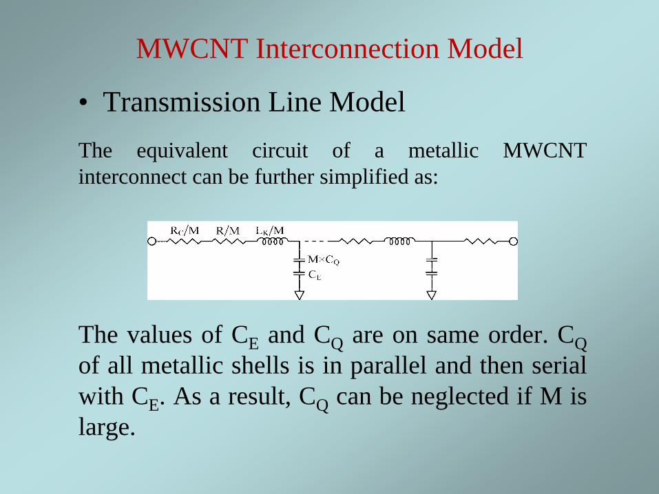
MWCNT Interconnection Model• Transmission Line Model
jiS DD
Cln
2 0
*S. Ramo, J. R. Whinnery, and T. V. Duzer, Fields and Waves in Communication Electronics, New York, Wiley, 1994.
MWCNT Interconnection Model
• Transmission Line ModelThe equivalent circuit of a metallic MWCNT interconnect can be further simplified as:
The values of CE and CQ are on same order. CQ of all metallic shells is in parallel and then serial with CE . As a result, CQ can be neglected if M is large.

SWCNT Bundle Interconnection Model
Cross-section of a SWCNT bundle interconnect.

Simplified equivalent circuit of a SWCNT bundle interconnect.
SWCNT Bundle Interconnection Model
• Transmission Line Model

MWCNT and SWCNT Bundle Interconnection• Simulation Results
The dimensions used in comparison correspond to 18, 22 and 32 nm diameters of the outermost shells of MWCNTs which also correspond to 18, 22, 32 nm CMOS technologies.
The length of MWCNTs used in calculations is 10 µm. Terminal impedance is set equal to contact resistance and D1 /DN = 2 and β = 1/3.
Ref 181: H. Li, et al., "Circuit modeling and performance analysis of multi- walled carbon nanotube interconnects," IEEE Transactions on Electron Devices, vol. 55, no. 6, pp. 1328-1337, June 2008.
Comparison of S21 and S11 from our model and Li et al. model for MWCNT interconnects: (a) amplitude and (b) phase
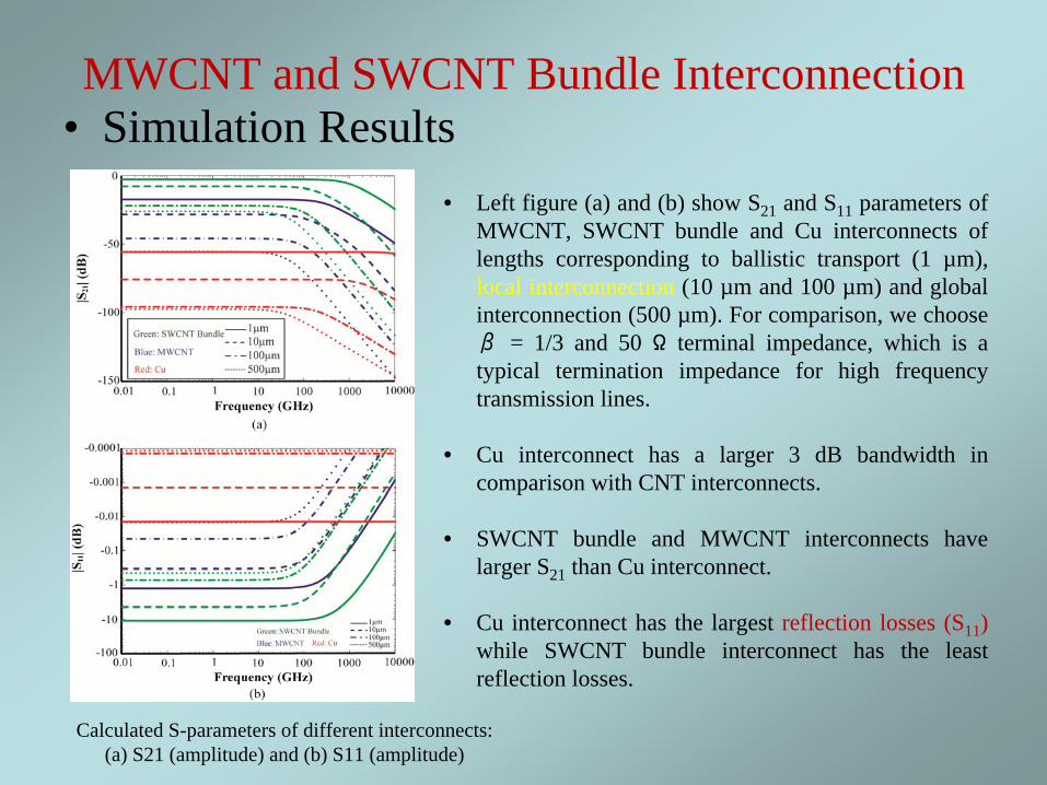
MWCNT and SWCNT Bundle Interconnection• Simulation Results
• Left figure (a) and (b) show S21 and S11 parameters of MWCNT, SWCNT bundle and Cu interconnects of lengths corresponding to ballistic transport (1 µm), local interconnection (10 µm and 100 µm) and global interconnection (500 µm). For comparison, we choose β
= 1/3 and 50 Ω
terminal impedance, which is a typical termination impedance for high frequency transmission lines.
• Cu interconnect has a larger 3 dB bandwidth in comparison with CNT interconnects.
• SWCNT bundle and MWCNT interconnects have larger S21 than Cu interconnect.
• Cu interconnect has the largest reflection losses (S11 ) while SWCNT bundle interconnect has the least reflection losses.
Calculated S-parameters of different interconnects: (a) S21 (amplitude) and (b) S11 (amplitude)

The increase in delay for Cu interconnects is larger than that of MWCNT and SWCNT bundle interconnects. The delays of MWCNT interconnects (β
= 1 and β
= 1/3) are smaller than that of SWCNT bundle and Cu interconnects. The delays are smaller for β
= 1 than for β
= 1/3 for both MWCNT and SWCNT bundle interconnects and is due to more interconnect channels with increase in β.
MWCNT and SWCNT Bundle InterconnectionSimulations Results
98

MWCNT and SWCNT Bundle Interconnection• Simulations Results
Type of CNT
Normalized Power Dissipation (%)
Length (µm)
1 10 100 500
MWCNT (β = 1) 0.070 0.065 0.339 1.422
MWCNT (β = 1/3) 0.359 0.418 2.182 7.591
SWCNT Bundle
(β = 1)0.011 0.015 0.079 0.137
SWCNT Bundle
(β = 1/3)0.036 0.047 0.256 0.688
Power dissipation ratio of MWCNT and SWCNT bundle to Cu interconnects:
Note: Normalization parameter is the length of Cu (1, 10, 100 and 500 µm). The technology node is 22 nm CMOS.

MWCNT and SWCNT Bundle Interconnection•• SummarySummary• MWCNT and SWCNT bundle interconnects exhibit higher transmission
efficiency and lower reflection losses and reduced power dissipation.
• With the increase in interconnection length, the delay of Cu interconnect increases faster than that of MWCNT and SWCNT bundle interconnects.
• For applications requiring small circuit delays MWCNT interconnects should be used due to smaller capacitances.
• Applications requiring large transmission efficiency and low reflection losses, CNT bundles should be used for interconnects.
• MWCNT and SWCNT bundle can replace Cu as interconnection wires in next generation of VLSI integrated circuits.

• Although we have compared our models of CNT interconnects with other proposed models; process variability effects are to be considered. .
• Reliability issues need to be considered since faults are likely to be present in the CNT based circuits.
• CMOS low power design techniques are to explored for CNT-based integrated circuits.
• CNT wire has reduced skin effect compared to metal conductors and has a great promise for realization of high-Q on-chip inductors for RF integrated circuits. [A. Srivastava et al, “CMOS LC Voltage Controlled Oscillator Design Using Carbon Nanotube Wire Inductors,” accepted for publication in ACM J. Emerging Technologies in Computing (special issue).]
• Experimental CNT based bio- and chemical sensors can be designed and developed based on the current research.
Scope of Future WorkScope of Future Work

AcknowledgementAcknowledgement
• Part of the research is supported by the United States Air Force Research Laboratory, Kirtland Air Force Base, New Mexico.
• My doctoral students: Jose M. Marulanda, Ph.D. (Electrical Engineering) August 2008; Yao Xu, Ph.D. (Electrical Engineering) May 2011; Yang Liu, Ph.D. (Electrical Engineering), expected December 2011; Rajiv Soundararajan, Ph.D. (Electrical Engineering), expected May 2012.
• US Air Force Research Laboratory colleagues: Dr. Ashwani K. Sharma, Clay Mayberry
• Research Grant from NSF-EPSCoR• Louisiana Economic Development Assistantship (2005-2009)
102

Selected Publications (Recent)• A. Srivastava, Y. Xu and A. K. Sharma, “Carbon nanotubes for next generation very large scale integration
interconnects,” J. Nanophotonics, (invited paper - online), special section on carbon nanotubes, vol. 4, 041690 (17 May 2010), pp. 1-26, 2010. DOI: 10.1117/1.3446896.
• Y. Xu and A. Srivastava, “A model for carbon nanotube interconnects,” Int. J. of Circuit Theory and Applications, vol. 38, Issue 6, pp. 559-575, 2010. Published online: 2 March 2009 by Wiley InterScience, DOI: 10.1002/cta.587, pp. 1-17, 2009.
• Y. Xu, A. Srivastava and A.K. Sharma, "Emerging carbon nanotube electronic circuits, modeling and performance," VLSI Design (invited paper - online), vol. 2010, Article ID 864165, pp. 1-8, 2010. DOI: 10.1155/2010/864165.
• A. Srivastava, J. Marulanda, Y. Xu and A. K. Sharma, “Current transport modeling of carbon nanotube field effect transistors,” physica status solidi (a), vol. 206, no. 7, pp. 1569-1578, 2009
• J. M. Marulanda, A. Srivastava and A.K. Sharma, “Threshold and saturation voltages modeling of carbon nanotube field effect transistors (CNT-FETs),” NANO, vol. 3, no. 3, pp. 195-201, 2008.
• J. M. Marulanda and A. Srivastava, “Carrier density and effective mass calculations in carbon nanotubes, physica status solidi (b), vol. 245, no. 11, pp. 2558-2562, 2008.
• A. Srivastava, Y. Xu, Y. Liu, A.K. Sharma and C. Mayberry, “CMOS LC voltage controlled oscillator design using carbon nanotube wire inductors,” invited paper submitted in a special issue of ACM Journal on Emerging Technologies, 2011. Part of the work is reported in Proc. of ISED 2010 (India) and IASTED ISCS 2010 (Hawaii).
• Yao Xu, “Carbon Nanotube Interconnect Modeling for Very Large Scale Integrated Circuits,” Ph.D. (Electrical Engineering) Dissertation, Louisiana State University, Baton Rouge, U.S.A., May 2011 (Major Advisor: Prof. Ashok Srivastava).
• Jose Mauricio Marulanda, “Current Transport Modeling of Carbon Nanotube Field Effect Transistors for Analysis and Design of Integrated Circuits,” Ph.D. (Electrical Engineering) Dissertation, Louisiana State University, Baton Rouge, U.S.A., August 2008 (Major Advisor: Prof. Ashok Srivastava).
103

Thank you!Thank you!