assessing and mitigating radiation effects in xilinx fpgas · assessing and mitigating radiation...
TRANSCRIPT

National Aeronautics and Space Administration
Assessing and Mitigating Radiation Effects in Xilinx FPGAs
Philippe Adell Jet Propulsion Laboratory
California Institute of Technology Pasadena, California
Greg Allen
Jet Propulsion Laboratory California Institute of Technology
Pasadena, California
Jet Propulsion Laboratory California Institute of Technology
Pasadena, California
JPL Publication 08-9 2/08


National Aeronautics and Space Administration
Assessing and Mitigating Radiation
Effects in Xilinx FPGAs
NASA Electronic Parts and Packaging (NEPP) Program Office of Safety and Mission Assurance
Philippe Adell Jet Propulsion Laboratory
California Institute of Technology Pasadena, California
Greg Allen
Jet Propulsion Laboratory California Institute of Technology
Pasadena, California
NASA WBS: 939904.01.11.30 JPL Project Number: 102197
Task Number: 3.18.4
Jet Propulsion Laboratory 4800 Oak Grove Drive Pasadena, CA 91109
http://nepp.nasa.gov
ii
This research was carried out at the Jet Propulsion Laboratory, California Institute of
Technology, and was sponsored by the National Aeronautics and Space Administration
Electronic Parts and Packaging (NEPP) Program.
Reference herein to any specific commercial product, process, or service by trade name,
trademark, manufacturer, or otherwise, does not constitute or imply its endorsement by
the United States Government or the Jet Propulsion Laboratory, California Institute of
Technology.
Copyright 2008. California Institute of Technology. Government sponsorship
acknowledged.
iii
TABLE OF CONTENTS
1 INTRODUCTION 1
2 XILINX FPGAS AND RADIATION EFFECTS 4 2.1 INTRODUCTION 4 2.2 XILINX SRAM FPGAS 5
2.2.1 PRODUCT DESCRIPTION 5 2.2.2 PRODUCT EVOLUTION 6 2.2.3 XILINX RADIATION ISSUES 6
3 RADIATION EFFECTS: TESTING METHODOLOGIES AND RESULTS 8 3.1 GENERAL RECOMMENDATION FOR TESTING XILINX FPGAS WITH HEAVY IONS 8 3.2 STATIC CHARACTERIZATION OF XILINX FPGAS 9
3.2.1 CONFIGURATION LOGIC BLOCKS AND BLOCK RAM 10 3.2.2 USER FLIP-FLOPS 10 3.2.3 HALF-LATCHES 11 3.2.4 SINGLE-EVENT FUNCTIONAL INTERRUPT (SEFI) TESTING 11 3.2.5 SINGLE-EVENT LATCH-UP TESTING 12
3.3 STATIC DATA ANALYSIS AND SIGNIFICANT RESULTS 12 3.3.1 CONFIGURATION-BIT CROSS SECTION 12 3.3.2 BLOCK RAM 13
3.4 DYNAMIC AND MITIGATED METHODOLOGIES 14 3.5 MULTIPLE-BIT UPSET: MBU 14
4 XILINX SRAM FPGAS MITIGATION TECHNIQUES 17 4.1 INTRODUCTION 17 4.2 MITIGATION BASICS 18
4.2.1 TRIPLE MODULAR REDUNDANCY (TMR) 18 4.2.2 CONFIGURATION SCRUBBING 20 4.2.3 TMRTOOL 21
4.3 MITIGATION: TECHNICAL ASPECTS 21 4.3.1 INPUT/OUTPUT 22
4.3.1.1 Signal Integrity—Inputs 22 4.3.1.2 Signal Integrity—Outputs 22
4.3.2 TMRTOOL—ASYNC DATA TRANSFER 23 4.3.2.1 TMRTool—ASYNC FIFO 24 4.3.2.2 Unaligned Clocks (Phase Shift between Clocks) 24
4.3.3 ADDITIONAL ISSUES RELATED TO TIMING CONSTRAINTS 26 4.3.3.1 XTMR Static Timing Constraints (1) 26 4.3.3.2 TMRTool—Beat Time 27 4.3.3.3 TMRTool Simulation 28
5 CONCLUSION 29
6 REFERENCES 30
1
1 INTRODUCTION
There are two main categories of radiation effects that are relevant for Static Random Access Memory (SRAM) Field-Programmable Gate Arrays (FPGAs) in space: Total-Dose Effects and Single-Event Effects (SEEs). Total-Dose Effects are cumulative effects that induce degradation of electrical parameters at the device, circuit, and system levels. They are induced by the total amount of ionizing energy deposited by photons or particles such as electrons, protons, or heavy ions. SEEs are induced by the passage of a single high energy proton or heavy ion through a device or a sensitive region of a microcircuit. SEEs in digital integrated circuits (ICs) can be either destructive (e.g., Single-Event Latch-up [SEL]), or non-destructive, such as the occurrence of transient faults in combinational and sequential logic. A good review of these effects (SEL, Single-Event Functional Interrupt [SEFI], Single-Event Transients [SET], Single-Event Upset [SEU], and Multiple-Bit Upset [MBUs]) with respect to different FPGA architectures can be found in [1].
This document provides an understanding of SEEs in FPGA components with a specific interest on Xilinx SRAM FPGAs. It also provides help to designers to identify appropriate testing and mitigation strategies to qualify these parts for space application.
FPGAs have been very attractive for space applications over the past decade. Indeed, the main advantage provided by gate arrays is the elimination of the large overhead cost (~ $250k) of developing custom application-specific integrated circuits (ASICs). Another advantage, provided by SRAM-configured gate arrays is the ability to reprogram existing devices, addressing evolving needs during hardware development or special requirements that are needed before and during a space mission.
Currently, the two main technologies that are used for FPGA devices are antifuse-based and SRAM-based. Many NASA systems have used gate arrays that employ antifuse technology, where permanent connections are programmed by high-current pulses that change the state of small regions in the gate array, making circuit connections. There are two primary antifuse technologies: oxide-nitride-oxide (ONO) and metal-to-metal (M2M). The ONO-based antifuse consists of a dielectric sandwich of silicon dioxide grown over the n-type antifuse diffusion, a silicon nitride layer, and another silicon dioxide layer. The ONO layer lies between a polysilicon conductor and a heavily doped n+ diffusion region of the base of the silicon wafer. When a programming voltage is applied, the ONO sandwich melts and a “bump” is formed into the polysilicon layer. The “bump” shatters the ONO layer, allowing diffusion of the substrate n+ into the polysilicon to form a low resistance path. The second antifuse switch, M2M, is constructed between two metal layers. The antifuse material is composed of layers of dielectrics and amorphous silicon. M2M antifuses hold an advantage over ONO as their programmed resistance is much lower, allowing for improved design performance. Antifuse technology has several inherent limitations that make SRAM-based FPGAs more attractive. First, once a device is programmed, it cannot be changed; additional devices have to be programmed and physically replace the installed devices. Second, available antifuse gate arrays are considerably smaller in gate count than SRAM-configurable gate arrays.
As in most competing technologies, there are engineering tradeoffs that designers must take into account. The one-time programmability that in some cases is seen as a
2
limitation gives way to SEU robustness. While offering the attractive feature of re-configurability, SRAM-configured gate arrays also have some limitations as well. They are not one-chip replacements for ASICs as they require off-chip configuration storage, typically an Electrically Erasable Read-Only Memory (EEPROM). Space-qualified versions of these devices are relatively expensive (~ $10k each). The SRAM in presently available devices is quite soft to upsets in the space radiation environment so that the functionality of a design can be broken due to an upset in the configuration.
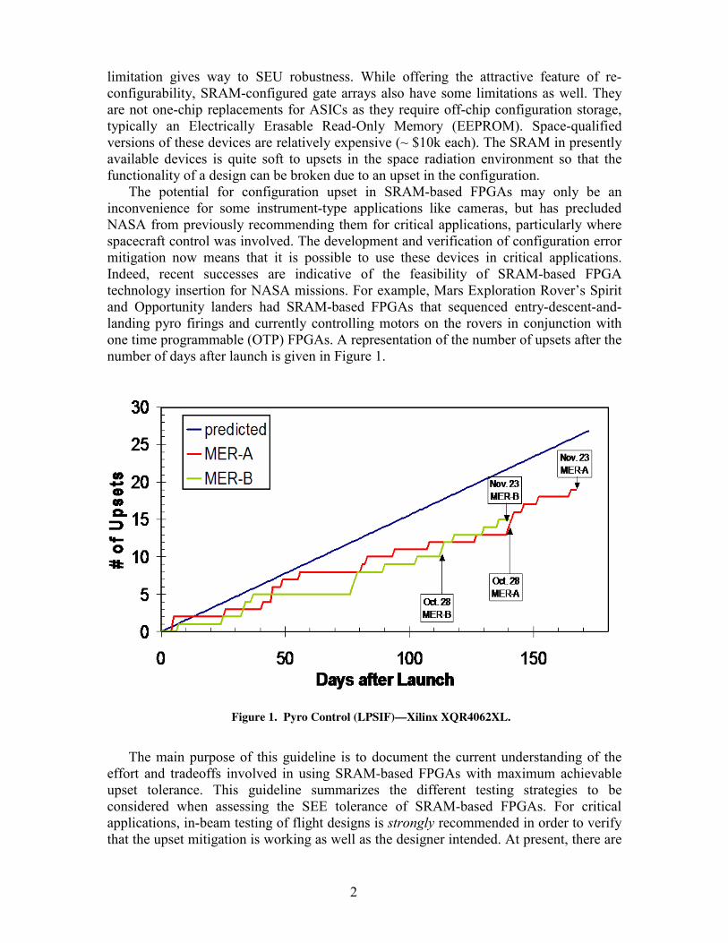
The potential for configuration upset in SRAM-based FPGAs may only be an inconvenience for some instrument-type applications like cameras, but has precluded NASA from previously recommending them for critical applications, particularly where spacecraft control was involved. The development and verification of configuration error mitigation now means that it is possible to use these devices in critical applications. Indeed, recent successes are indicative of the feasibility of SRAM-based FPGA technology insertion for NASA missions. For example, Mars Exploration Rover’s Spirit and Opportunity landers had SRAM-based FPGAs that sequenced entry-descent-and-landing pyro firings and currently controlling motors on the rovers in conjunction with one time programmable (OTP) FPGAs. A representation of the number of upsets after the number of days after launch is given in Figure 1.
Figure 1. Pyro Control (LPSIF)—Xilinx XQR4062XL.
The main purpose of this guideline is to document the current understanding of the
effort and tradeoffs involved in using SRAM-based FPGAs with maximum achievable upset tolerance. This guideline summarizes the different testing strategies to be considered when assessing the SEE tolerance of SRAM-based FPGAs. For critical applications, in-beam testing of flight designs is strongly recommended in order to verify that the upset mitigation is working as well as the designer intended. At present, there are
3
four manufacturers (Actel, Xilinx, Atmel, and Aeroflex) offering six FPGA types to the military market (i.e., some military spec screening and testing are specified) and four device types to the aerospace application market, which indicates that the manufacturers have added radiation parameter specifications. There is also a Honeywell and BAE Systems device that has been under development for several years, but it does not appear to be available yet; inquiries to Honeywell’s military/aerospace marketing arm on this product have been unanswered.
4
2 XILINX FPGAS AND RADIATION EFFECTS
2.1 Introduction
Field-Programmable Gate Arrays (FPGA) are configurable integrated circuits based on a high logic density regular structure, which can be customizable by the end user to realize different designs. The FPGA architecture is based on an array of logic blocks and interconnections customizable by programmable switches. Several different programming technologies are used to implement the programmable switches. There are three types of such programmable switch technologies currently in use:
• ANTIFUSE, when an electrically programmable switch forms a low resistance path between two metal layers. o ACTEL
o AEROFLEX
• FLASH, where the switch is a floating gate transistor that can be turned off by injecting charge onto the floating gate. o ACTEL
• SRAM, where the programmable switch is usually a pass transistor or multiplexer controlled by the state of a Static Random Access Memory (SRAM) bit (SRAM-based FPGAs) o ATMEL
o XILINX
Customizations based on SRAMs are volatile. This means that SRAM-based FPGAs can be reprogrammed as many times as necessary in-situ and that they lose their contents information when the memories are powered “OFF.” The antifuse customizations are non-volatile, holding the customizable content even when not connected to the power supply and being able to be programmed just once. Each FPGA has a particular architecture. Programmable logic companies such as Xilinx, Actel, Aeroflex (under license with Quicklogic FPGAs), Atmel, and Honeywell (under license with Atmel FPGAs) offer radiation-tolerant FPGA families. Each company uses different mitigation techniques to better take into account the architecture characteristics. The following sections provide details, testing procedures, experimental results, and mitigation strategies to help designers qualify these devices in a space radiation environment.
5
2.2 Xilinx SRAM FPGAs
2.2.1 Product Description
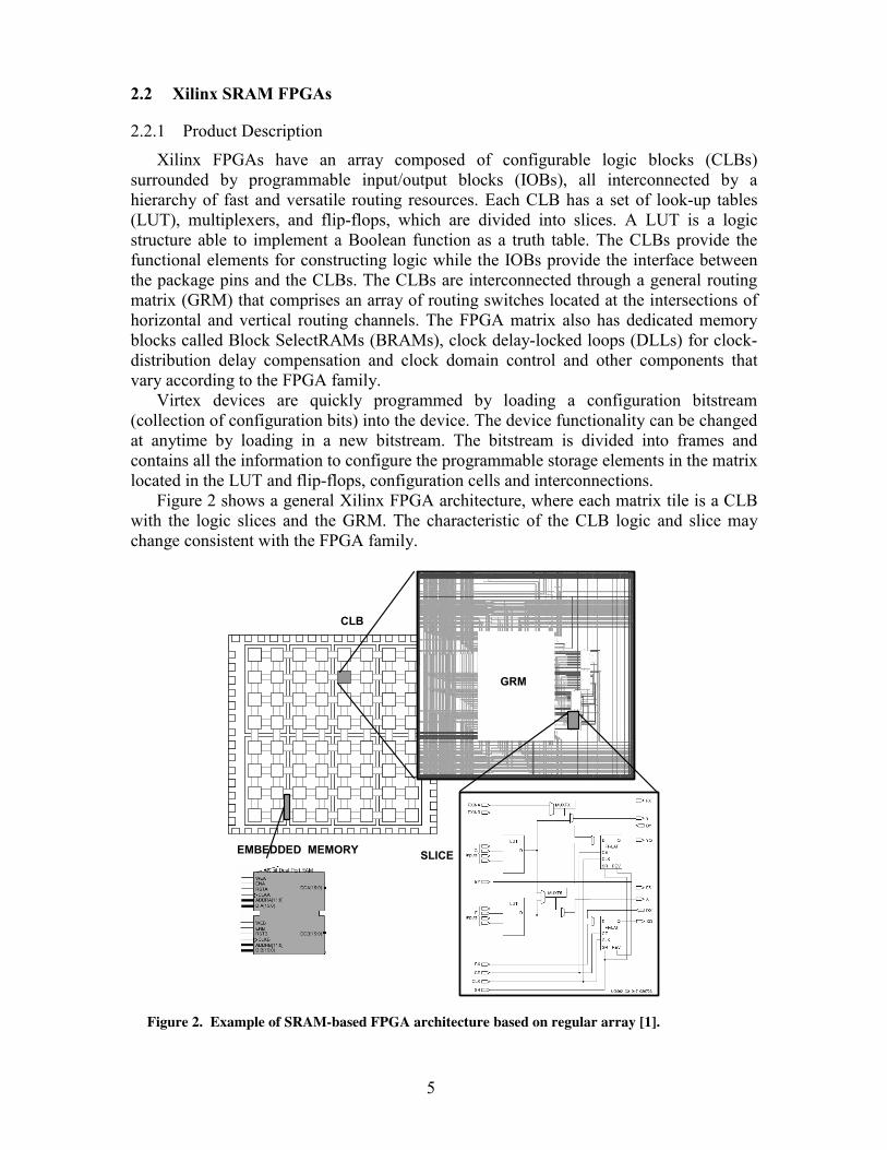
Xilinx FPGAs have an array composed of configurable logic blocks (CLBs) surrounded by programmable input/output blocks (IOBs), all interconnected by a hierarchy of fast and versatile routing resources. Each CLB has a set of look-up tables (LUT), multiplexers, and flip-flops, which are divided into slices. A LUT is a logic structure able to implement a Boolean function as a truth table. The CLBs provide the functional elements for constructing logic while the IOBs provide the interface between the package pins and the CLBs. The CLBs are interconnected through a general routing matrix (GRM) that comprises an array of routing switches located at the intersections of horizontal and vertical routing channels. The FPGA matrix also has dedicated memory blocks called Block SelectRAMs (BRAMs), clock delay-locked loops (DLLs) for clock-distribution delay compensation and clock domain control and other components that vary according to the FPGA family.
Virtex devices are quickly programmed by loading a configuration bitstream (collection of configuration bits) into the device. The device functionality can be changed at anytime by loading in a new bitstream. The bitstream is divided into frames and contains all the information to configure the programmable storage elements in the matrix located in the LUT and flip-flops, configuration cells and interconnections.
Figure 2 shows a general Xilinx FPGA architecture, where each matrix tile is a CLB with the logic slices and the GRM. The characteristic of the CLB logic and slice may change consistent with the FPGA family.
GRM
CLB
SLICEEMBEDDED MEMORY
Figure 2. Example of SRAM-based FPGA architecture based on regular array [1].
6
The main functional elements in Xilinx devices are comprised of IOBs and internal functional blocks (IFBs).
The digitally controlled Impedance (DCI) input/output (I/O) feature automatically provides on-chip termination for each I/O element. More information can be found in the following Xilinx application notes [2].
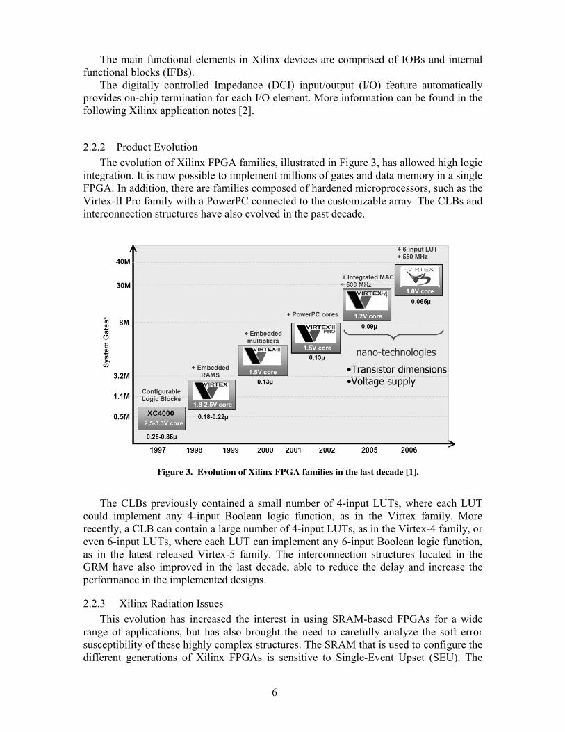
2.2.2 Product Evolution The evolution of Xilinx FPGA families, illustrated in Figure 3, has allowed high logic
integration. It is now possible to implement millions of gates and data memory in a single FPGA. In addition, there are families composed of hardened microprocessors, such as the Virtex-II Pro family with a PowerPC connected to the customizable array. The CLBs and interconnection structures have also evolved in the past decade.
nano-technologies
•Transistor dimensions•Voltage supply
Figure 3. Evolution of Xilinx FPGA families in the last decade [1].
The CLBs previously contained a small number of 4-input LUTs, where each LUT
could implement any 4-input Boolean logic function, as in the Virtex family. More recently, a CLB can contain a large number of 4-input LUTs, as in the Virtex-4 family, or even 6-input LUTs, where each LUT can implement any 6-input Boolean logic function, as in the latest released Virtex-5 family. The interconnection structures located in the GRM have also improved in the last decade, able to reduce the delay and increase the performance in the implemented designs.
2.2.3 Xilinx Radiation Issues This evolution has increased the interest in using SRAM-based FPGAs for a wide
range of applications, but has also brought the need to carefully analyze the soft error susceptibility of these highly complex structures. The SRAM that is used to configure the different generations of Xilinx FPGAs is sensitive to Single-Event Upset (SEU). The
7
effect of these upsets on the configurations depends on the application in which the FPGA device is implemented, including the number of configurations.
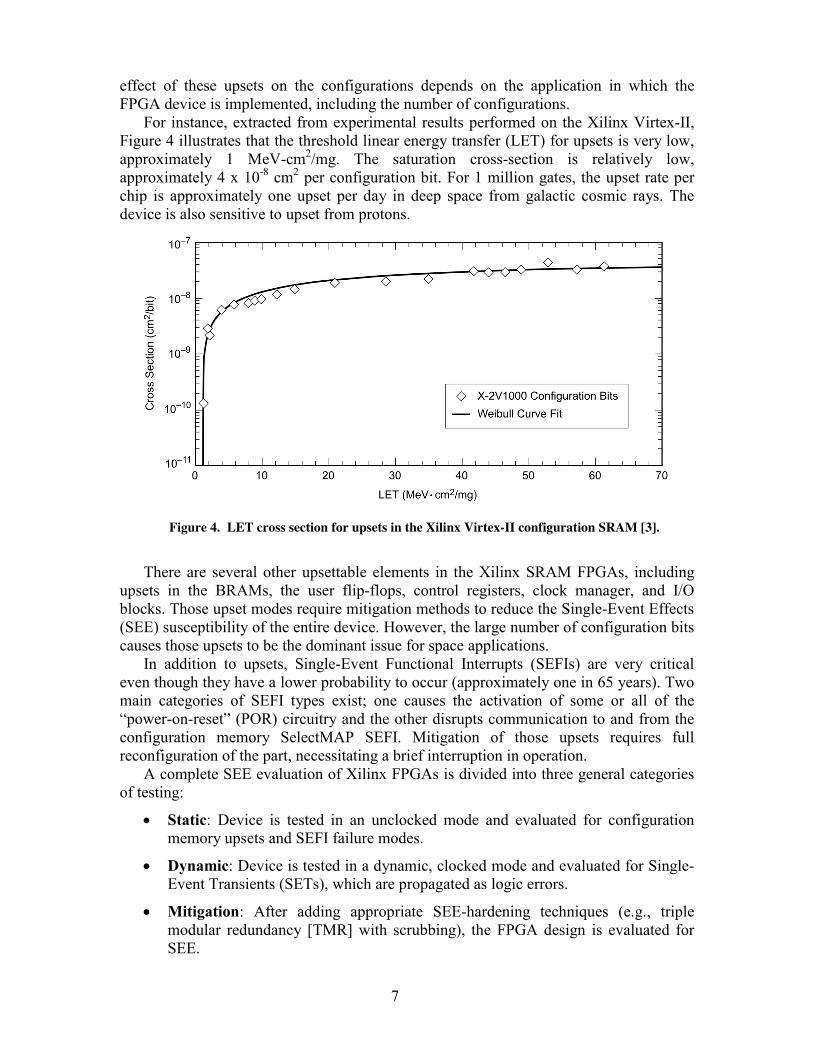
For instance, extracted from experimental results performed on the Xilinx Virtex-II, Figure 4 illustrates that the threshold linear energy transfer (LET) for upsets is very low, approximately 1 MeV-cm2/mg. The saturation cross-section is relatively low, approximately 4 x 10⁻⁸ cm2 per configuration bit. For 1 million gates, the upset rate per chip is approximately one upset per day in deep space from galactic cosmic rays. The device is also sensitive to upset from protons.
Figure 4. LET cross section for upsets in the Xilinx Virtex-II configuration SRAM [3].
There are several other upsettable elements in the Xilinx SRAM FPGAs, including
upsets in the BRAMs, the user flip-flops, control registers, clock manager, and I/O blocks. Those upset modes require mitigation methods to reduce the Single-Event Effects (SEE) susceptibility of the entire device. However, the large number of configuration bits causes those upsets to be the dominant issue for space applications.
In addition to upsets, Single-Event Functional Interrupts (SEFIs) are very critical even though they have a lower probability to occur (approximately one in 65 years). Two main categories of SEFI types exist; one causes the activation of some or all of the “power-on-reset” (POR) circuitry and the other disrupts communication to and from the configuration memory SelectMAP SEFI. Mitigation of those upsets requires full reconfiguration of the part, necessitating a brief interruption in operation.
A complete SEE evaluation of Xilinx FPGAs is divided into three general categories of testing:
• Static: Device is tested in an unclocked mode and evaluated for configuration memory upsets and SEFI failure modes.
• Dynamic: Device is tested in a dynamic, clocked mode and evaluated for Single-Event Transients (SETs), which are propagated as logic errors.
• Mitigation: After adding appropriate SEE-hardening techniques (e.g., triple modular redundancy [TMR] with scrubbing), the FPGA design is evaluated for SEE.
8
3 RADIATION EFFECTS: TESTING METHODOLOGIES AND RESULTS
Verifying Xilinx Static Random Access Memory (SRAM)-based Field-Programmable Gate Arrays (FPGAs) for use in space applications is a very convoluted and complex process. After the devices are prepared for irradiation, the primary concern for space qualification is their invulnerability to Single-Event Latch-up (SEL). This process involves biasing the device under test (DUT) with the appropriate bias conditions, irradiating the devices at heavy ion and/or protons facilities, and observing various device conditions. If the device survives an SEL screening, the single-event susceptibility for the smallest obtainable storage elements should be defined. Once the storage elements (i.e., Configuration Logic Blocks [CLBs], Block RAMs [BRAMs], and User Flip-Flops [DFFs], etc.) have been characterized, various dynamic building blocks must be dynamically exercised and characterized for any Single-Event Functional Interrupt (SEFI) modes and finally appropriate mitigation techniques must be developed.
3.1 General Recommendation for Testing Xilinx FPGAs with Heavy Ions
As a general rule, parts to be tested at heavy ion facilities need to be de-lidded to simulate the effect of heavy ions from a space environment. Most heavy ions available at most accelerator facilities (i.e., Brookhaven National Laboratory [BNL] and the Texas A&M Cyclotron [TAM]) do not have the ion ranges to reach the active region of the device if irradiated with the lid on. In addition, Xilinx SRAM FPGA devices are manufactured in a flip-chip geometry. This means that to obtain a comprehensive linear energy transfer (LET) vs. cross-section representation, devices need to be thinned from the backside of the chip.
Most of Single-Event Effects (SEE) testing performed on different families of Xilinx SRAM-based FPGAs have shown that a nominal range value of 80 µm above the active region is sufficient to acquire the most desired effective LETs and still maintain a minimum range through the active region [4]. Most SEE assessments indicated that very little (~negligible) lot-to-lot variation in the cross-section curves was observed. It was found that cross-section vs. LET representations are very similar when comparing the sensitivity of commercial devices to thin-epitaxial military/aerospace devices [5]. Therefore, test samples manufactured with the same fabrication process are representative of the entire Xilinx device family.
To obtain good statistics, it is also recommended to test at least two devices for Single-Event Upset (SEU) / SEFI evaluations and three parts for SEL. Bias conditions are also critical for a good SEE evaluation. For all static and SEFI characterization, it is recommended that the core and input/output (I/O) voltages be set to the specified minimum according to the manufacturer’s data sheet. During Latch-up testing it is recommended that the device be biased at the specified maximum voltages, the junction temperature elevated, and the temperature monitored. The voltages should be measured as close to the DUT as possible (e.g., on bypass capacitors) as there is often a voltage drop from the power supply to the DUT when drawing a large amount of current. It should also be noted that the ability to change and record bias conditions at the beam facilities is a very cost-effective approach.

9
Due to the extensive range requirements resulting from irradiating through the back of the DUT, if an effective LET vs. cross-section characterization or latchup testing is required, a facility should be selected with the following characteristics: high energy, long range ions that will penetrate the silicon backside and through the entire active region at high effective LETs. If a mitigation test is being performed, then the beam acts as a random fault injection engine and flux replaces effective LET as the cross-section variable.
The selection of an ion’s flux is fully dependent on the desired event being captured. This is discussed below in more detail. However, it can be stated that ion flux should be such that events cannot overlap each other and the event rate does not overwhelm the device tester, but is high enough to acquire sufficient event statistics in a reasonable amount of time. A mitigated test will be completely flux dependent, at which point beam uniformity and a static flux becomes very important. A mitigated test requires three fluxes, approximately an order of magnitude apart from each other, and is fully described in [3]. The total fluence, per effective LET data point, is a function of event counting statistics. The accuracy of one cross-section vs. effective LET curve and therefore subsequent rates are only as accurate as the data points that make up that curve. Therefore, as a general rule it is suggested that a minimum of 100 events be counted. If the number of 100 events is not practical, a minimum fluence of 107 ions/cm2 should be subjected to the DUT. It should also be noted that a very high fluence of ions (necessary for SEFI characterization) will generate a significant amount of total ionizing dose (TID) and impact the SEU characterization and cross section. Although accelerated, average doses won’t impact the electrical characteristics of the DUT in the same manner as a uniform, low-dose deposition, it is recommended that the accrued total dose not exceed the device’s manufacturer specified total dose.
3.2 Static Characterization of Xilinx FPGAs
Xilinx FPGA Static characterization is based on the ability to isolate the various memory or storage components of the FPGA and extract upset data from the desired element. A configuration manager is a necessary building block to ensure correct device functionality under irradiation and to isolate upsets in the configuration from other target storage elements. The configuration manager should provide SEFI detection and take corrective actions when a SEFI is detected. A detailed implementation of a configuration manager is beyond the scope of this document (the manufacturer provides several application notes on device scrubbing and will soon provide a complete Virtex-4 configuration manager application note, complete with VHSIC hardware description language [VHDL]), but it should at the least provide the following functionalities:
• The ability to readback and compare the configuration logic of the device and determine/accumulate upsets.
• The ability to scrub the device with correct data (although it is not necessary to have knowledge of an upset to scrub, i.e., “blind scrubbing”).
• Minimal SEFI detection—if the functionality of the device or the ability to communicate in any manner with the device stops, the monitor should be able to
10
detect this and perform the correct action to regain complete functionality, visibility of the “prog” and “done” pins, etc.
A complete static characterization consists of obtaining cross-section vs. LET representation with good statistics for: 1) SEL at high and low temperature, 2) SEFI, 3) CLBs, BRAMs, and DFF and Half-Latches (Weak Keeper Circuits). Every test follows a particular procedure detailed below.
3.2.1 Configuration Logic Blocks and Block RAM
The CLBs and BRAMs are the fundamental building blocks and storage elements that will define the inherent, unmitigated upset susceptibility of the device. There are several techniques available to acquire the desired information. The first technique requires no configuration manager, and simply consists of programming the device with a known, static design, irradiating, and reading back the upset bitstream using Xilinx’s configuration software. Extracting the upset data then requires knowledge of the location of bits in the bitstream, along with a custom script to extract that information. The bitstream can also be sent to Xilinx to have the desired upset data extracted. A second technique is to use a custom configuration manager to read the desired device frames, then parse and accumulate an instantaneous upset count. No matter the means by which bitstream data is extracted, the following test procedure is recommended:
• Program and verify DUT • Irradiate DUT • Record DUT conditions, readback data, and any other anomalous behavior • Power cycle, adjust effective LET, and repeat as necessary For this characterization, due to the inherent sensitivity and sheer number of bits, it is
recommended that around 1000 upsets be accumulated for both CLBs and BRAM cross sections. Typical fluences necessary to acquire proper statistics lay in the range of 5×10³ to 105
particle/cm2, depending on the effective LET. The average sensitivity for both ones and zeros for CLBs can be represented as a single cross-section vs. effective LET plot with little loss to conservatism. However, a true representation of the static sensitivity of BRAMs requires two designs, one where the BRAM is filled with zeros and one where the BRAM is filled with ones.
3.2.2 User Flip-Flops Static characterization of user flip-flops requires a configuration manager and
working scrubber, to ensure that upsets in the configuration will not be clocked into the flip-flops and that the design remains uncorrupted while upsets are accumulated. A typical design should include several shift register chains, utilizing as many flip-flops as possible. The tester should be able to choose the pattern that is shifted through the register chains, and functional monitoring should take place out of the beam (whether in external software through digital acquisition software, in a service FPGA, or in some combination). Experience has shown that there can be small subsets of bits that will either set or reset large subsets of flip-flops. It is necessary to count this SEFI mode, but
11
important to extract this from the static upset characterization. The following test procedure is suggested:
• Program and verify DUT • Fill shift register chain with the desired pattern • Irradiate DUT for a period to accumulate errors, but still be able to distinguish
single upsets as opposed to set/reset SEFIs • Pause beam, flush out shift registers, and record upsets (noting number of upsets
and judging number, if any, of set/reset SEFIs) • Resume beam and repeat above step until at least 100 events are recorded • Adjust effective LET and repeat as necessary
This characterization typically requires a low flux such that consecutive low fluence runs can be executed and single-bit upsets can be differentiated from SEFIs. Due to the asymmetry that exists in the upset sensitivity between ones and zeros for the user flip-flops, the user design should be able to fill the shift registers with either ones or zeros.
3.2.3 Half-Latches
The motivation behind half-latch testing is not to characterize the susceptibility of the week keeper circuit, but to characterize the recovery time of the circuit. This can be achieved in a similar manner to the flip-flop characterization, but is done dynamically. Details of half-latch testing can be found in [3], but patterns of ones and zeros are driven through long shift register chains, and compared on the output. If there is a persistent error in the pattern, it means a half latch is upset and not recovering.
Typically, half-latch designs can be tested with high fluxes and, due to the small or null cross sections of stuck persistent upsets, require high fluences. The half-latch design is often used as the functional counterpart during SEFI testing, due to the high fluences also required for SEFI testing.
3.2.4 Single-Event Functional Interrupt (SEFI) Testing SEFI detection and characterization is an evolutionary process for every new device.
In general, SEFIs on Xilinx devices are caused by configuration control logic, communication (joint test action group [JTAG] or SelectMAP [SMAP]) logic, and various other global logic control circuitry. The number of bits that control this logic is relatively small, and so the cross-section for these events is also relatively low. During SEFI detection, the flux should be set as high as possible without allowing SEFI events to overlap (a rate of about one SEFI every 30 seconds is appropriate). During SEFI testing, fluences in the magnitude of 107 ions/cm2 will be reached per run; as such, total dose should be monitored closely and DUTs replaced as necessary. Thus far, SEFIs have shown no apparent design dependencies. Yet the tester should be cognizant of the fact that the design in place during SEFI testing should try to exercise as much of the device as possible in order to maintain visibility of SEFIs that are not detected by the configuration manager.
12
3.2.5 Single-Event Latch-up Testing
Although no latch-up has been visible throughout the testing of Virtex FPGAs, it is important to continue to rule it out. Testing is performed with the device biased at the specified maximum voltages, an observed junction temperature of at least 120°C, and with the highest obtainable effective LETs without limiting the ion range. There is no limiting flux parameter for SEL testing on Xilinx devices (as long as SELs are not occuring). It is recommended that fluences of 107 ions/cm2 be subjected upon the device. There is no known design dependency for SEL on Xilinx devices, but in order to reach high device temperatures, specific designs are used. One such design toggles every flip-flop in the DUT, increasing current consumption, and therefore power and temperature.
3.3 Static Data Analysis and Significant Results
Complicated devices such as FPGAs often yield complex data reduction tasks. Upon collection of the data, any observed anomalies or SEFI events need to be noted, counted, and removed from the static storage elements cross section.
3.3.1 Configuration-Bit Cross Section
On the surface, characterizing the configuration bits of a Xilinx device seems as simple as an SRAM static irradiation, whereby the tester programs the device, irradiates, reads the values after irradiation, and counts the errors. In Xilinx devices the ability to read the bitstream out of the device is possible with Xilinx’s iMPACT programming software. It is very important that the tester be cognizant of the device status, preferably during, but at the minimum, after irradiation. As a baseline of observation, the tester should record and monitor the device’s control and status registers (accessible through iMPACT) and monitor the device’s DONE pin. If an upset occurs that alters the state of the aforementioned registers, that run should be discarded and the run repeated. Figure 5 shows an example of cross-section vs. effective LET representation that has been obtained to characterize the configuration bits in Virtex-4. Results are also compared to Virtex-II. Although the LET threshold has not changed from Virtex-II to Virtex-4, where the cross-section in Virtex-II is effectively saturated, Multiple-bit Upset (MBU) has made an apparent lack of saturated cross-section very evident in Virtex-4 devices.

13
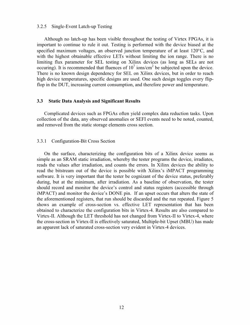
3.3.2 Block RAM
BRAM-static cross sections are acquired in a similar manner to configuration-bit cross sections. The same care must be taken to look for device SEFIs and extract corrupted data. In addition to the device-level SEFIs, BRAM may have its own specific SEFI mode related to BRAM data integrity bits. If these data integrity bits are upset, it may lead to the device addressing the BRAM differently, thereby changing the number of apparent upsets (i.e., BRAM that was not intended to be accessed will report an incorrect value).
Xilinx Virtex-4 Heavy Ion Average SEU Configuration Cross Section
10-6
10-7
10-8
10-9
10-
0 20 40 60 80 100 120Effective LET (MeV*cm2/mg)
SX55 CLB AVGFX60 CLB AVGLX200 CLB AVGV2 WeibullV4 Weibull
Figure 5. Configuration bit cross-section versus effective LET.
14
3.4 Dynamic and Mitigated Methodologies
In general, dynamic and mitigated testings are very application specific, and are bound by engineering, performance, and mitigation trade-offs [6]. In general, a dynamically implemented component (i.e., Digital Clock Managers [DCM], Digital Signal Processing [DSPs], processors, etc.) is functionally exercised and observed for any upset or SEFI behaviors. Once cross sections have been determined for the functional blocks, a mitigation scheme should be developed, which may include all or combinations of triplication, scrubbing, watchdog timers, and management circuitry. A system error rate should be determined following the guidelines found in [7]. Cross sections for mitigated systems are plotted against flux, and error rates are determined via the methodologies defined in [7].
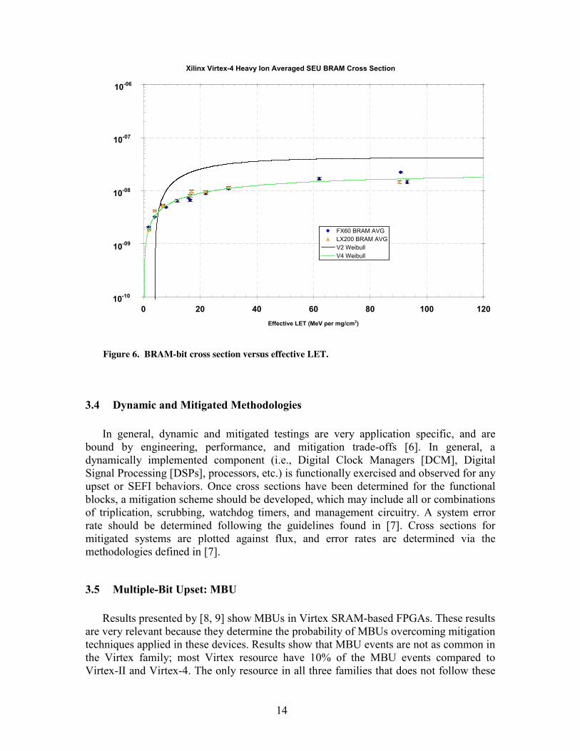
3.5 Multiple-Bit Upset: MBU
Results presented by [8, 9] show MBUs in Virtex SRAM-based FPGAs. These results are very relevant because they determine the probability of MBUs overcoming mitigation techniques applied in these devices. Results show that MBU events are not as common in the Virtex family; most Virtex resource have 10% of the MBU events compared to Virtex-II and Virtex-4. The only resource in all three families that does not follow these
Xilinx Virtex-4 Heavy Ion Averaged SEU BRAM Cross Section
10-06
10-07
10-08
10-09
10-10
0 20 40 60 80 100 120Effective LET (MeV per mg/cm2)
FX60 BRAM AVGLX200 BRAM AVGV2 WeibullV4 Weibull
Figure 6. BRAM-bit cross section versus effective LET.
15
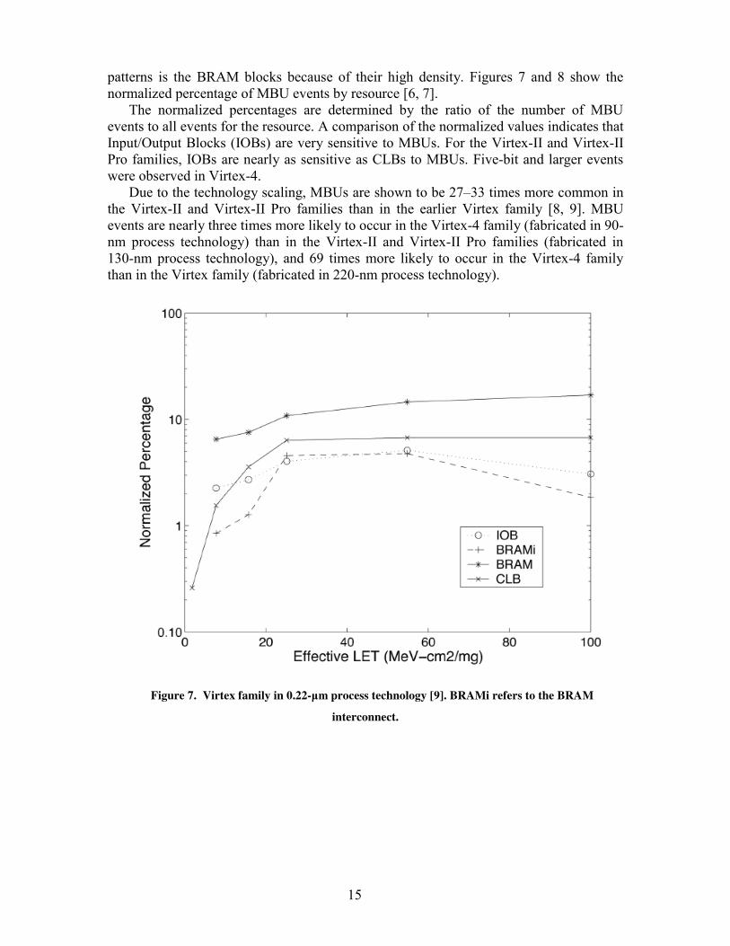
patterns is the BRAM blocks because of their high density. Figures 7 and 8 show the normalized percentage of MBU events by resource [6, 7].
The normalized percentages are determined by the ratio of the number of MBU events to all events for the resource. A comparison of the normalized values indicates that Input/Output Blocks (IOBs) are very sensitive to MBUs. For the Virtex-II and Virtex-II Pro families, IOBs are nearly as sensitive as CLBs to MBUs. Five-bit and larger events were observed in Virtex-4.
Due to the technology scaling, MBUs are shown to be 27–33 times more common in the Virtex-II and Virtex-II Pro families than in the earlier Virtex family [8, 9]. MBU events are nearly three times more likely to occur in the Virtex-4 family (fabricated in 90-nm process technology) than in the Virtex-II and Virtex-II Pro families (fabricated in 130-nm process technology), and 69 times more likely to occur in the Virtex-4 family than in the Virtex family (fabricated in 220-nm process technology).
Figure 7. Virtex family in 0.22-μm process technology [9]. BRAMi refers to the BRAM
interconnect.
16
Figure 8. Virtex-II family in 0.13-μm process technology [9].
17
4 XILINX SRAM FPGAS MITIGATION TECHNIQUES
4.1 Introduction
The design at the high-level description (VHSIC Hardware Description Language [VHDL] or Verilog) level can be protected by using some redundancy techniques targeting the Field-Programmable Gate Array (FPGA) architecture. The most popular high-level Single-Event Upset (SEU) mitigation technique currently used to protect designs synthesized in the SRAM-based FPGAs is triple modular redundancy (TMR) combined with scrubbing. Xilinx has released the tool called X-TMR that automatically implements TMR into the user description [10]. The user himself can also implement TMR in his design. However, due to the high area overhead of TMR, some alternative solutions have been proposed in recent years. Therefore, the user has the flexibility of implementing duplication and self-checking techniques instead of TMR. These techniques may compromise the fault tolerance at some point, but the final result may be acceptable for a set of applications.
In this way, it is possible to use a commercial FPGA part to implement the design and the soft error mitigation technique is applied to the design description before being synthesized in the FPGA. The user has the flexibility of choosing the fault-tolerant technique and consequently the overheads in terms of area, performance, and power dissipation. One very important step of the design flow is the validation of the fault tolerance technique, which is usually done by fault injection. The original bitstream configured into the FPGA can be modified by a circuit or a tool in the computer by flipping the bitstream bits, one at a time. This flip emulates a SEU in the configuration memory cells. The output of the design under test (DUT) can be constantly monitored to analyze the effect of the injected fault into the design. If an error is detected, this means that the fault-tolerant technique implemented is not robust for that specific fault (SEU) in that target-configuration memory bit.
It is possible to inject faults in all the configuration bits and to analyze the most critical parts of the design [11, 12, 13]. This can help to guide designers in the early stages of the development process to choose the most appropriate fault-tolerant design, even before any radiation ground testing. The entire fault injection campaign can take a few hours to days depending on the number of bits that are going to be flipped and the connection to the fault injection control circuit. When the entire system (fault injection control + DUT + golden designs) is implemented at the hardware level (board), avoiding the communication with the computer, the process is sped up by orders of magnitude. The process needs to be always finalized by appropriate single-event testing.
In addition, FPGA devices contain important functional blocks that can be upset by radiation; once this occurs, the effects can be catastrophic. Consequently, the susceptibility of these functional blocks must also be analyzed and mitigation techniques must be applied. Examples include Digital Clock Managers (DCMs), which provide phase-locked, skew-corrected clock signals to all parts of the chip; Phase-Matched Clock Dividers (PMCDs), which offer additional frequency division options; configuration controller circuit; power-on-reset (POR) circuitry; Input/Output Blocks (IOBs), which implement 28 common single-ended or differential (in pairs) input/output (I/O) standards with digitally controlled impedance; XtremeDSP (DSP48) slice, which contains a
18
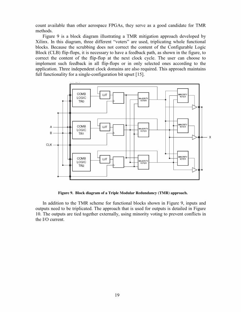
dedicated 18x18-bit multiplier, adder; and 48-bit accumulator and other specialized blocks. Table 1 presents a summary of Single-Event Effect (SEE) issues and possible SEU mitigation solutions [14].
Table 1. Xilinx Virtex Family Potential Types of Device SEE Sensitivity: Summary
FPGA component parts SEE Issues Possible SEU mitigations Configuration Memory Single and multiple bit errors corrupting
circuit operation, causing bus conflicts (current creep), modifications in the logic, etc…
Scrubbing Partial reconfiguration
Configuration Controller Improper device configuration can occur if hit during configuration/reconfiguration
Partitioned design Multiple chip voting (Redundancy by using multiple devices)
CLB Logic hits and propagated upsets caused by transients
Triple modular redundancy (TMR) Acceptable error rates
BRAM Memory upsets in user area TMR Error Detection and Correction (EDAC) scrubbing
Half-latches Sensitive structure used in configuration/routing
Removal of half-latches from design
POR SEUs on POR can cause inadvertent reboot of device
Multiple chip voting (Redundancy by using multiple devices)
IOB SEUs can cause false outputs to other devices or inputs to logic
TMR Leverage Immune Config. Memory cell Evaluate input SET propagation
DCM Can cause clock errors that spread across clock cycles
TMR Temporal TMR
DSP Hard IP that is unhardened that can cause single event functional interrupts (SEFIs) or data errors
TMR Temporal TMR
MGT Gigabit transceivers. Hits in logic can cause bursts or SEFIs. O/w bit errors in data stream
TMR Protocol re-writes
PPC Hard IP that is unhardened. SEFIs are prime concern
Processor duplication or software task redundancy
The following section reviews most of the mitigation techniques that can be applied
on FPGA.
4.2 Mitigation Basics
4.2.1 Triple Modular Redundancy (TMR)
TMR is a common hardening technique that can be implemented via design synthesis to reduce the SEE susceptibility of FPGA parts. Since Xilinx FPGAs have a larger gate
19
count available than other aerospace FPGAs, they serve as a good candidate for TMR methods.
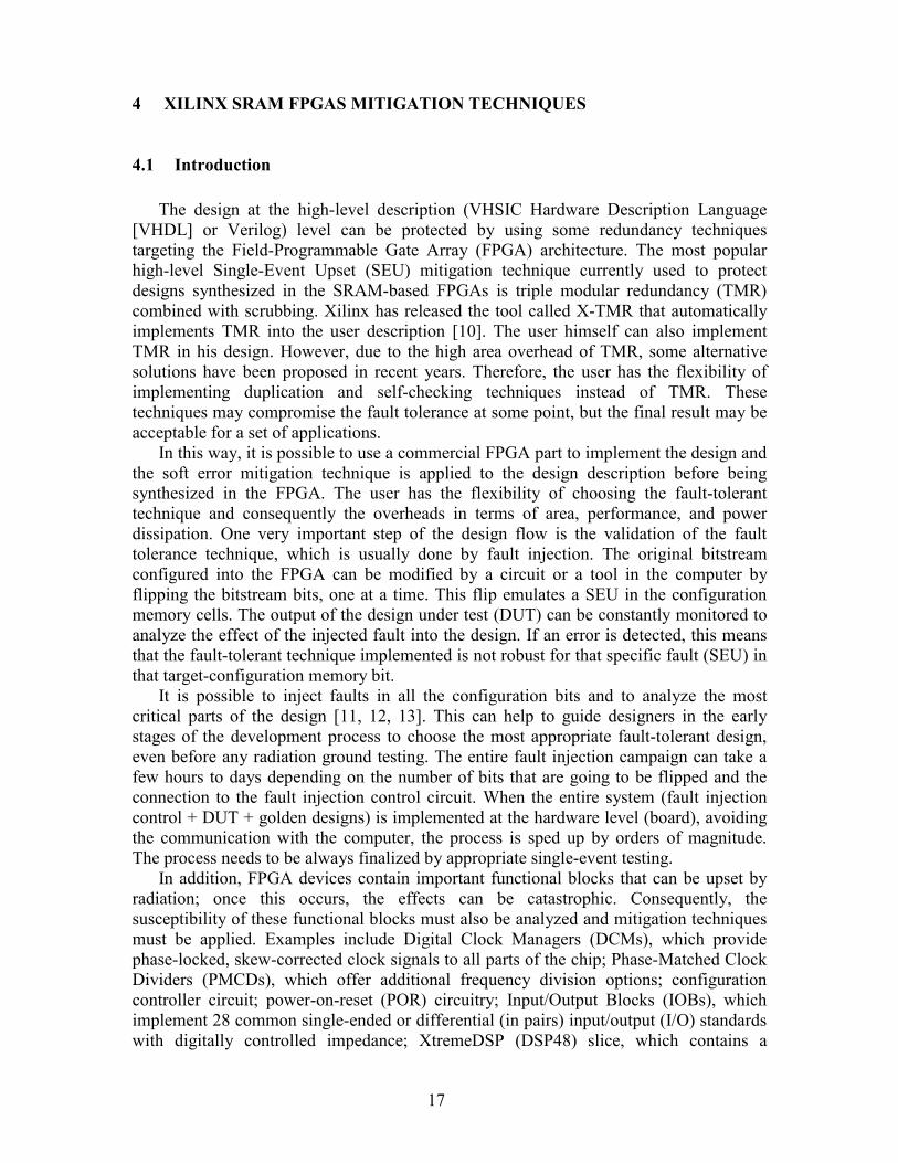
Figure 9 is a block diagram illustrating a TMR mitigation approach developed by Xilinx. In this diagram, three different “voters” are used, triplicating whole functional blocks. Because the scrubbing does not correct the content of the Configurable Logic Block (CLB) flip-flops, it is necessary to have a feedback path, as shown in the figure, to correct the content of the flip-flop at the next clock cycle. The user can choose to implement such feedback in all flip-flops or in only selected ones according to the application. Three independent clock domains are also required. This approach maintains full functionality for a single-configuration bit upset [15].
Figure 9. Block diagram of a Triple Modular Redundancy (TMR) approach.
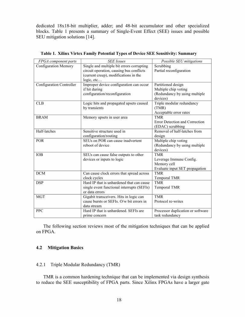
In addition to the TMR scheme for functional blocks shown in Figure 9, inputs and outputs need to be triplicated. The approach that is used for outputs is detailed in Figure 10. The outputs are tied together externally, using minority voting to prevent conflicts in the I/O current.
20
Figure 10. Approach used to triplicate outputs, including minority voting scheme.
4.2.2 Configuration Scrubbing
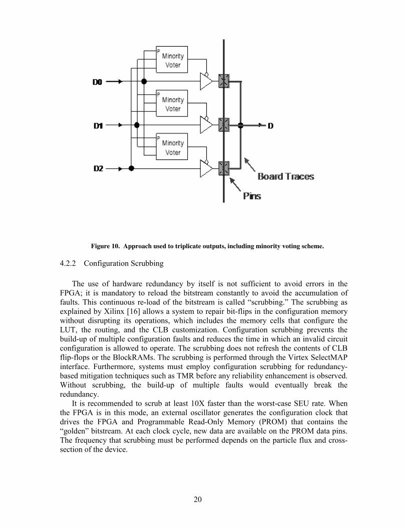
The use of hardware redundancy by itself is not sufficient to avoid errors in the FPGA; it is mandatory to reload the bitstream constantly to avoid the accumulation of faults. This continuous re-load of the bitstream is called “scrubbing.” The scrubbing as explained by Xilinx [16] allows a system to repair bit-flips in the configuration memory without disrupting its operations, which includes the memory cells that configure the LUT, the routing, and the CLB customization. Configuration scrubbing prevents the build-up of multiple configuration faults and reduces the time in which an invalid circuit configuration is allowed to operate. The scrubbing does not refresh the contents of CLB flip-flops or the BlockRAMs. The scrubbing is performed through the Virtex SelectMAP interface. Furthermore, systems must employ configuration scrubbing for redundancy-based mitigation techniques such as TMR before any reliability enhancement is observed. Without scrubbing, the build-up of multiple faults would eventually break the redundancy.
It is recommended to scrub at least 10X faster than the worst-case SEU rate. When the FPGA is in this mode, an external oscillator generates the configuration clock that drives the FPGA and Programmable Read-Only Memory (PROM) that contains the “golden” bitstream. At each clock cycle, new data are available on the PROM data pins. The frequency that scrubbing must be performed depends on the particle flux and cross-section of the device.
21
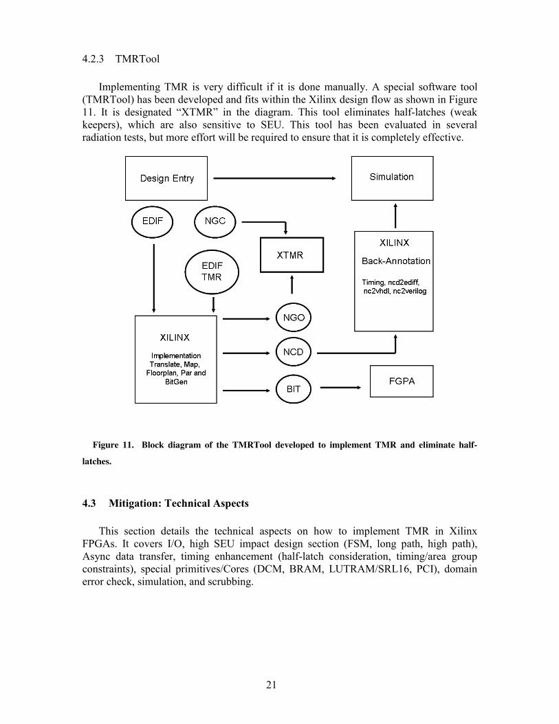
4.2.3 TMRTool
Implementing TMR is very difficult if it is done manually. A special software tool (TMRTool) has been developed and fits within the Xilinx design flow as shown in Figure 11. It is designated “XTMR” in the diagram. This tool eliminates half-latches (weak keepers), which are also sensitive to SEU. This tool has been evaluated in several radiation tests, but more effort will be required to ensure that it is completely effective.
Figure 11. Block diagram of the TMRTool developed to implement TMR and eliminate half-
latches.
4.3 Mitigation: Technical Aspects
This section details the technical aspects on how to implement TMR in Xilinx FPGAs. It covers I/O, high SEU impact design section (FSM, long path, high path), Async data transfer, timing enhancement (half-latch consideration, timing/area group constraints), special primitives/Cores (DCM, BRAM, LUTRAM/SRL16, PCI), domain error check, simulation, and scrubbing.
22
4.3.1 Input/Output
4.3.1.1 Signal Integrity—Inputs
It is recommended that the TMR input fan-out points be located as close as possible to the FPGA device, not only to help reduce the printed circuit board (PCB) board congestion, but also to help with the timing due to trace skew. It is even more critical if the inputs are for clock signals where trace -length matching is crucial for proper functionality. Therefore, it is important to select the input pins on the package to be as close as possible. The inputs can then be treated as one node for signal integrity (SI) analysis. Related to FPGA, PACE (ISE tool) is the useful tool that displays the package view (both top and bottom view) for designers to quickly identify what pins to assign. It also performs basic simultaneous switching output (SSO) analysis.
4.3.1.2 Signal Integrity—Outputs
It is also recommended that a TMR output be merged as soon as possible. This helps reduce the reflection of the traces due to the skew from the device to the package and skew due to the PCB layout. If the merging of the TMR outputs cannot be controlled, the ringing due to the reflection might be worse. Connecting three outputs is not recommended by SI experts. This approach raises many questions regarding device reliability; even with a perfectly constrained design, there is a good chance of output skew due to the package. In this case, one output will start driving the opposite value of the other two. This is followed by two outputs driving against the last one that’s yet to switch. Finally, all three outputs will settle at the same value.
Xilinx IOBs are built with numerous metal layers to accommodate the many I/O standards that it supports. The Xilinx devices undergo stringent qualifications where outputs are purposely tied to opposite values to ensure IOB integrity. Therefore, any two I/Os will not be able to damage another I/O, and electromigrations are not of concern.
When designing, it is important to adjust SSO parameters for the V2 CF package since the package capacitors are removed. For designs running less than 100 MHz, the difference can be ignored. Xilinx does provide Input/Output Buffer Information Specification (IBIS) and Spacecraft, Planets, Instrument, C-matrix, Events (SPICE) models so that simulation can be performed to ensure SI. One solution that can be used to improve the reflection and to ensure better SI is to place a series-termination resistor at the downstream-receiving device of the Xilinx TMR outputs. Table 2 summarizes the strength and weakness of the TMR I/O scheme.
23
Table 2. TMR—Input/Output Strengths and Weaknesses
XTMR Output Type Pros Cons Don’t touch
• Minimal resource utilization • Can pack DDR or output registers
in IOB • Easy PCB layout
• Highly vulnerable to SEU/SET
Converge
• Minimal resource utilization • Can pack DDR or output registers
in IOB • Easy PCB layout
• Vulnerable to SEU/SET
Triplicated, Unvoted
• Can pack DDR or output registers in IOB
• High immunity against SEU/SET
• High device utilization • Requires extensive PCB layout
consideration for SI Triple-Voted
• High immunity against SEU/SET • High device utilization • Requires extensive PCB layout
consideration for SI • Inability to insert DDR or output
register into output IOB
Double-Voted
• High immunity against SEU/SET • Not as much resource utilization
• Medium device utilization • Requires extensive PCB layout
consideration for SI • Inability to insert DDR or output
register into output IOB Custom
• Allows user to tailor the output type for any specific need
• May require a fair amount of work to plan and implement
4.3.2 TMRTool—Async data transfer
Asynchronous data transfer is a design challenge for TMR applications. To ensure correct data throughput, grey encode and decode are implemented. However, this process cannot be constrained by timing constraints. As a result, although the First In, First Out (FIFO) pipelines are fed by the same clock and data, the outputs may be off by 1 or 2 clock cycles, and the effective TMR scheme will be compromised.
Various mitigation options can be considered at this point and are described as follows:
1) Choose not to apply TMR on the FIFO and take the cross-section hit. 2) Partially apply TMR [17] on the FIFO. 3) Fully apply TMR on the FIFO and utilize problem detection and reset.
24
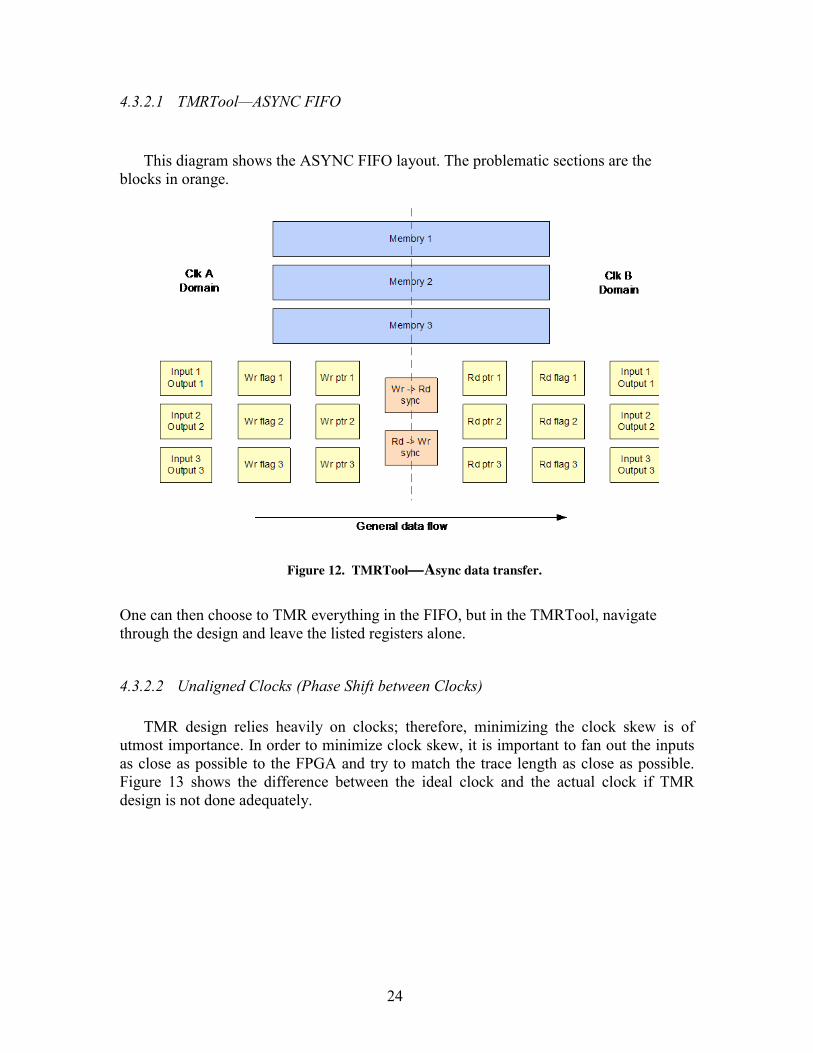
4.3.2.1 TMRTool—ASYNC FIFO
This diagram shows the ASYNC FIFO layout. The problematic sections are the
blocks in orange.
Figure 12. TMRTool—Async data transfer.
One can then choose to TMR everything in the FIFO, but in the TMRTool, navigate through the design and leave the listed registers alone.
4.3.2.2 Unaligned Clocks (Phase Shift between Clocks)
TMR design relies heavily on clocks; therefore, minimizing the clock skew is of utmost importance. In order to minimize clock skew, it is important to fan out the inputs as close as possible to the FPGA and try to match the trace length as close as possible. Figure 13 shows the difference between the ideal clock and the actual clock if TMR design is not done adequately.

25
Figure 13. Schematic representation of the clock alignment issue when applying TMR.
The direct consequence of a misalignment between clocks is that it can cause some SI
problems at the output. An example is given in Figure 14. In some cases, race conditions might occur if clocks are really out of phase. For instance, for the V2 Xilinx FPGA, a phase shift of more than 0.44 ns could create problems. A smaller number makes the design more vulnerable to timing failure. It is possible to enter the board skew with the latest Xilinx Integrated Software Environment (ISE) tool used, but overall, the PCB skew is still of the utmost importance.
Figure 14. Example of signal integrity due to misalignment between the clocks.
26
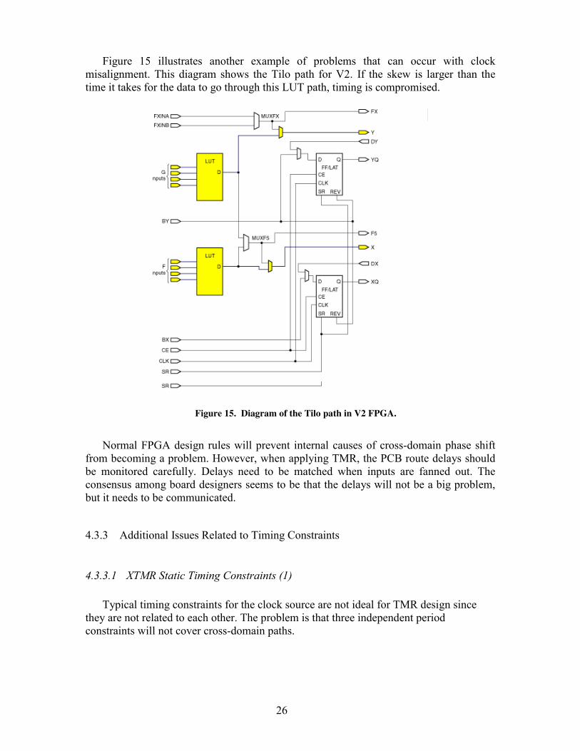
Figure 15 illustrates another example of problems that can occur with clock misalignment. This diagram shows the Tilo path for V2. If the skew is larger than the time it takes for the data to go through this LUT path, timing is compromised.
Figure 15. Diagram of the Tilo path in V2 FPGA.
Normal FPGA design rules will prevent internal causes of cross-domain phase shift
from becoming a problem. However, when applying TMR, the PCB route delays should be monitored carefully. Delays need to be matched when inputs are fanned out. The consensus among board designers seems to be that the delays will not be a big problem, but it needs to be communicated.
4.3.3 Additional Issues Related to Timing Constraints
4.3.3.1 XTMR Static Timing Constraints (1)
Typical timing constraints for the clock source are not ideal for TMR design since they are not related to each other. The problem is that three independent period constraints will not cover cross-domain paths.

27
Figure 16. XTMR Static Timing Constraints.
An example of how to relate the period constraints is given in Figures 16 and 17.
Timing analysis and Place and Route (PAR) can correctly place and route the design to ensure design functionality.
Figure 17. XTMR Static Timing Constraints.
4.3.3.2 TMRTool—Beat Time
Meeting the timing constraints is not easy, particularly for TMR designs. For some of the Virtex generations, half-latch extraction is necessary (V2, V2P, V4). Typically, applying TMR in the V2 design becomes a challenge over 100 MHz. In addition, options such as half-latch extraction will create routing burden and make timing constraints even harder to meet. Some tradeoffs need to be considered; this is the designer’s responsibility. For instance, in the case of V2 it has been found that the stuck half latch has a cross
28
section about 1 order of magnitude lower than that for SEFI. For V2P and V4, all half latch errors will recover.
One could also help PAR meet timing and minimize MBU impact by assigning Area Group constraints. PAR traditionally has a tough time placing BRAM for optimal timing performance. By manually placing BRAM, timing may be improved.
Although the DCM is useful, it can be upset and cause the loss of clock outputs altogether. Therefore, good reset logic should be developed to ensure integrity of the DCM. A quick custom mitigation scheme for the DCM may involve a simple counter comparator to track the DCM output. It is also important to avoid the listed DCM outputs because DCM generates these outputs on the rising edge of CLKIN. Therefore, it is possible that if DCM loses and regains its input clock, the listed output clock could be misaligned.
The Virtex-4 has a GLUTMASK setting such that configuration skips SRL16/LUTRAM data. Scrub or readback will result in ‘0’; thus allowing the user to implement SRL16/LUTRAM in design. However, the user must ensure the data is constantly flowing since scrubbing will not correct the content of these components.
For Virtex-2, such a setting does not exist; therefore, scrubbing will corrupt SRL16/LUTRAM. TMRTool automates extraction of SRL16, and the user should take care of extraction of LUTRAM with a custom macro using user flip-flops.
TMR PCI design would be challenging. The Xilinx 33MHz V2 PCI core can likely meet timing constraints with proper care of offset constraints (i.e., not triplicating the I/Os) and the use of parity bit.
4.3.3.3 TMRTool Simulation
Simulation not only serves as a good bench test, it also ensures the proper functionality and has the ability to reproduce timing performance of a design with a reasonable level of accuracy. Another advantage of simulation is that the effect of an upset in the logic can be simulated and mitigated. It allows one to purposely insert/force incorrect data input, to pause/resume clock in each domain, or to reset each domain to test finite state machines (FSM), etc. Hardware solutions are also available, such as a fault injection test and a smoke test.
29
5 CONCLUSION
When dealing with Xilinx Field-Programmable Gate Arrays (FPGAs), depending on the application, it is important to evaluate the appropriate level of upset mitigation that is needed:
• None: if rate is acceptable and application is NOT critical • Detection only: reconfigure upon an upset • Full mitigation: design-level triple modular redundancy (TMR) and configuration
scrubbing
When the appropriate level of upset mitigation is selected, it is important to choose an appropriate implementation for detection or scrubbing:
• Internal: still requires, at least, an external watchdog timer • External: upset-hardened application-specific integrated circuit (ASIC) or one-
time programmable (OTP) FPGA
The reconfigurable logic within Static Random Access Memory (SRAM)-based FPGAs that provides system designers with flexibility and processing power is also the device’s greatest weakness if not properly mitigated against Single-Event Effects (SEEs). The main purpose of TMR is to ensure correct system-level operation when there is a single-bit upset. Correctly implemented TMR can only ensure correct design operation for one or fewer configuration upsets. In order to prevent the accumulation of upsets, a scrubbing algorithm is necessary. It is strongly recommended not to use TMR or scrubbing alone. Although design trade-offs must be taken into consideration, system-level mitigation is most effective when deployed together.
Despite the fact that the TMR technique has proven successful in the test cases that have been evaluated to date, it is also highly recommended that actual flight designs be subjected to radiation testing to verify that the specific design features used in the implementation are consistent with the TMR tool. As shown in this guideline, applying appropriate mitigation techniques requires a lot of technical attention. This document has provided the major points to be considered when applying TMR (timing constraints, signal integrity, clock alignments, etc.). Simulation has shown some successful debugging and reveals design or TMR issues. It should be noted that synthesis implementation can be optimized and can affect the design. Functional simulation success does not equal timing simulation success.
In summary, there is no “hardening by design” solution that is completely efficient for all types of circuits, applications, and environments. It is important to characterize the sensitivity to soft error of the target design and application, and then to choose a set of fault-tolerant solutions that will work properly within the constraints of the design. The ideal solution for a reliable system may be composed of solutions that pass at different steps of the design processes (i.e., layout constraints, transistor-level redundancy, logic-level solutions, re-computation, and system-level approaches).
30
6 REFERENCES [1] NSREC short course, 2007.
[2] Xilinx Inc. Virtex® Series Datasheets and Application Notes, www.xilinx.com, 2006.
[3] "Virtex-II Static Characterization," Xilinx Single Event Effects Consortium, 2004, http://parts/docs/swift/virtex2_0104.pdf.
[4] Swift, G.M., and A.H. Johnston, “Practical Aspects of Single Event Testing: Experimental Planning and Interpretation,” RADECs 2007 short course, to be published in transaction on Nucl. Sci.
[5] George, J., R. Koga, G. Swift, G. Allen, C. Carmichael, and C. Tseng, “Single Event Upsets in Xilinx Virtex-4 FPGA Devices,” IEEE Radiation Effects Data Workshop, 2006, pp. 109–114.
[6] G.M. Swift, S. Rezgui, J. George, and C. Carmichael, “Dynamic Testing of Xilinx Virtex-II Field Programmable Gate Array (FPGA) Input/Output Blocks (IOBs),” IEEE Transactions on Nuclear Science, Vol. 51, No. 6, 2004.
[7] Edmond, L. “Analysis of SEU Rates in TMR devices.” Unpublished document.
[8] Quinn, H., and P. Graham, "Terrestrial-Based Radiation Upsets: A Cautionary Tale," IEEE Symposium on Field-Programmable Custom Computing Machines, 2005.
[9] Quinn, H., P. Graham, J. Krone, M. Caffrey, and S. Rezgui, “Radiation-induced multi-bit upsets in SRAM-based FPGAs,” in IEEE Transactions on Nuclear Science, Vol. 52, Issue 6, Dec. 2005, pp. 2455–2461.
[10] TMRTool user guide, Version 6.2.3, Xilinx Inc., Sept. 2006, http://www.xilinx.com/products/milaero/ug156.pdf.
[11] Berg, M., “Fault Tolerance Implementation within SRAM Based FPGA Design Based upon the Increased Level of Single Event Upset Susceptibility,” in IEEE International On-line Test Symposium, IOLTS, 2006, pp. 89–91.
[12] Kastensmidt, F., G. Neuberger, L. Carro, R. Reis, and R. Hentschke, “Designing Fault-Techniques for SRAM-based FPGAs,” IEEE: Design and Test of Computers (D&T), Vol. 21, No. 6, Dec. 2004.
[13] Reorda S., L. Sterpone, and M. Violante, “Efficient estimation of SEU effects in SRAM-based FPGAs,” 11th EEE International On-line Testing Symposium, 2005, pp. 54–59.
[14] Label K., M. Berg, D. Black, W. Robinson, and A. Jordan, “Trade Space Involved with Single Event Upset (SEU) and Transient (SET) Handling of Field Programmable Gate Array (FPGA) Based Systems,” 2006 Workshop on Hardened Electronics and Radiation Technology (Heart), 2006.
31
[15] Carmichael C. XAPP197, “Triple Modular Redundancy Design Techniques for Virtex FPGAs,” June 2006, http://www.xilinx.com/support/documentation/application_notes/xapp197.pdf.
[16] Carmichael C., Caffrey M., and Salazar A., XAPP216, “Correcting Single Event Upsets through Virtex Partial Configuration,” June 2000, http://www.xilinx.com/support/documentation/application_notes/xapp216.pdf.
[17] Pratt, B., M. Caffrey, P. Graham, K. Morgan, and M. Wirthlin, “Improving FPGA Design Robustness with Partial TMR,” 44th Annual IEEE International Reliability Physics Symposium Proceedings, 2006, pp. 226–232.