astronomical detectors. the first detector in astronomy eye: complete system of telescope (variable...
TRANSCRIPT

Astronomical Detectors

The First Detector in Astronomy
Eye: complete system of telescope (variable aperture, ~1cm max), detector, and data reduction processor
Retina• Light sensitive, chemical process
Rods• 100 million• 2m wide
• can detect low light levels
• averted vision
Cones
• color information
• 7 million
• cluster near axis
• 1000 per square mm
Reusable
• integration times 100 ms
Quantum efficiency ~1%
Resolution 80 arcsecs
Discoveries made with the Eye
Naked Eyes
• Nomenclature: Constellations, star names
• Astrometry: Stellar positions
• Magnitude scale
• Planets in solar system, planet orbits (Tycho, Kepler)
• Comets
• Supernovae explosions, variable stars
• Sunspots (by Chinese 800 B.C.)
• Solar corona (eclipse)
• Lunar Phases
• Star Clusters (e.g. Pleiades)

Discoveries made with the Eye
With telescopes
• Sunspot cycle
• Saturn‘s rings, Jupiter‘s Red Spot
• Nebulae, Spiral Nebulae
• Parallax, astrometric measurements
• Asteroids, moons of most planets
• Craters on Moon

Observations with the eye can be unreliable
• No record of observations so as to check results
• Precise measurements cannot be made (position, magnitude, etc) because observations are not recorded or digitized
• Integration time of eye is short so faint objects cannot be seen without using larger and larger telescopes
Example of unreliability of eye: Canals on Mars

Ground-based CTIO 4m
Hubble Space Telescope
Eta Carinae Images over the past 100 years

• 1840 J.W. Draper makes a photograph of the moon. Followed by photographs of the Sun by Foucault and Fizeau
• Sunspots photographed in 1858 by W. De La Rue
• Jansen and Lockyer in the 1870s photographed the solar spectrum and discovered the spectral lines of Helium.
• Ainsee Common photographed Orion Nebula and these revealed stars and details you could not see in a telescope
• Photographs by Hubble in the early 1900‘s established that some nebula where „island universes“ (i.e. galaxies). His spectral observations of galaxies (exposures of more than one night) led to the discovery of the expansion of the Universe.
• For 100 years photographic plates/film dominated the field of astronomical detectors.
A Revolution in Detectors: Photographic Plates

• Photomultiplers are photon counting devices that consist of vacuum tube with a photocathode and focusing electrodes for amplification.
• Photocathode: light striking the photocathode produces an electron through the photoelectric effect
• Focusing electrodes focus the electron toward electron multiplier or dynode. Each dynode is held at a more positive voltage as the previous one
• Electrons are accelerated as they approach the first dynode arriving with greater energy.
• More low energy electrons are released and acclerated by the second dynode.
•A cascade amplifies the number of electrons (1 photon can produce up to 108 electrons)
• At anode an electric current is produced
Single Channel Detectors: Photomultiplier Tubes

In 1907 Joel Stebbins pioneered the use of photoelectric devices in Astronomy

Spectral response of some commonly used photocathode materials

Photomultiplier tubes: pile up errors
Each detected photon produces a pulse of finite duration, t0, which causes a dead time in the detector. The number of pulses (exposure time) is reduced by the amount of overlapping deadtimes.
N = n/(1–t0n)
N is the true rate, and n the apparent rate
Pile-up errors System blocks completely at
high light levels

Disadvantages of Photomultiplier tubes:
• Must be operated at high voltages
• High light levels can destroy the tube
• Not very efficient in optical regions: 3500 to 10.000 Ang.
• Single channel devices (more on this later)

Multi-Channel Detectors (Arrays): Photographic Plates
Advantages of photographic plates:
• Wide field of view. TLS Schmidt plates are 3 deg x 3 deg.
• Resolution, more so than a CCD of the same area
Photographic plates were the first two-dimensional detectors

Disadvantages of photographic plates:
• Low quantum efficiency. The best plates have a QE of about 3%
• Long exposure times, inefficient use of time
• Reciprocity failure. It becomes less effective as exposure time increases
• Non-linear color sensitivity. Plates are more sensitive to blue light
• Hypersensitising and Developing. Hypersensitising involves baking plates to increase efficiency (up to 10%). You cannot see results until after developing usually many hours later.
• Storage. They are fragile and take up space. They also decay with age.
• Digitisation. Must be scanned to put the data in digital form
• Cost and availability. In 1996 a single 30 cm x 30 cm plate costs $100 USD. Kodak no longer makes plates.
So why do we not still use plates?

Reciprocity Failure of Photograhic Plates
Cross section of a photographic plate

CCD: The Digital Revolution
• CCD = Charge Coupled Device
- A photon detecting device that exploits the photoelectric effect and the semiconducting properties of silicon
- The voltage generated is coupled to the intensity of the incident light
• Pixel = picture element. Each pixel is an independent photon detector
• DN = Data Number (ADU = Analog to Digital Unit)
- The output signal from a CCD. Value and range depend on the nature of the voltage digitization. E.g. an 8-bit CCD produces DNs from 0 to 28 (0 to 255). Most CCDs are 16 bit (maximum = 65535) or higher
Nomenclature:

CCD Properties and Definitions

Material Eg (eV) max (Å)
Pure Si 1.1 11300
GaAs 1.43 8670
InSb 0.36 34400
max = 12400 Å/Eg

n-type: a material with more than 4 valence electrons is added (As, from group Va). The extra electrons cannot be accommodated in the valence band and so occupy the conduction band. They represent a persistent set of negative carriers
p-type: a material with fewer than 4 valence electrons is added (e.g. B, from group IIIa). This has one fewer electron than normal and creates a small "vacuum" in the electron sea of the valence band. This is called a "hole." As valence electrons shift to fill it, the hole propagates like a positive charge in the opposite direction. The holes represent a persistent set of positive carriers.
From http://www.astro.virginia.edu/class/oconnell/astr511/lec11-f03.html

In the depletion region a photon produces an electron. This migrates into the conduction band
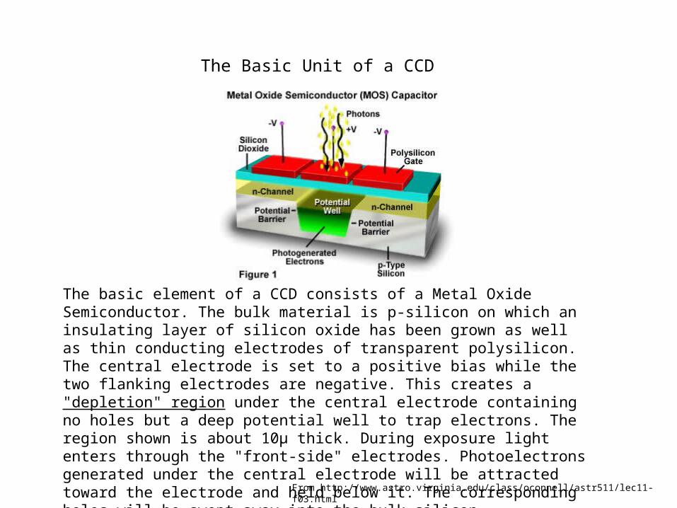
The Basic Unit of a CCD
The basic element of a CCD consists of a Metal Oxide Semiconductor. The bulk material is p-silicon on which an insulating layer of silicon oxide has been grown as well as thin conducting electrodes of transparent polysilicon. The central electrode is set to a positive bias while the two flanking electrodes are negative. This creates a "depletion" region under the central electrode containing no holes but a deep potential well to trap electrons. The region shown is about 10µ thick. During exposure light enters through the "front-side" electrodes. Photoelectrons generated under the central electrode will be attracted toward the electrode and held below it. The corresponding holes will be swept away into the bulk silicon.
From http://www.astro.virginia.edu/class/oconnell/astr511/lec11-f03.html

Reading out a CCD
Parallel registers shift the charge along columns
There is one serial register at the end which reads the charge along the final row and records it to a computer
A „3-phase CCD“
ColumnsFor last row, shift is done along the row

The CCD is first clocked along the parallel register to shift the charge down a column
The CCD is then clocked along a serial register to readout the last row of the CCD
The process continues until the CCD is fully read out.
Figure from O‘Connell‘s lecture notes on detectors


How much charge is lost in the this charge transfer process?
Typical Charge Transfer Efficiency of a CCD is >99.999 %
Suppose you have a 4096 x 4096 CCD and detect 40.000 photons (electrons). Signal to Noise ratio = √N = 200
Charge recorded = 40.000 x 0.999994096 = 38.394
1605 electrons „lost“
S/N decreased to 195

Typical CCD readout times are 90 – 240 secs, depending on the size of the CCD. This is for single amplifier CCDs. To reduce the readout time some devices can have 4 channels (amplifiers) for readout:
Serial register with one amplfier
Normal readout
4 Serial registers with 4 amplfiers
4 Channel CCD
4 channel CCD cuts readout time by a factor of 4. Problem: each quadrant usually behaves differently, with its own bias, flat field response, etc. In the data reduction 4 channel CCDs have to be reduced as if they were 4 independent frames.

Quantum Efficiency of some science grade CCDs from ESO:
The real power of CCDs is their high quantum efficiency

Quantum Efficiency of CCDs compared to other devices

Two basic types of CCDs:
Front illuminated CCD: A CCD whose gate structure is located in front of the potential wells. In other words the light has to pass through the gates
Back illuminated CCD: A CCD whose thickness is reduced to 10 m so that it can be focused on the front where there are no gates. A back illuminated CCD is just a front illuminated CCD flipped and thinned. It is more efficient, particularly in the blue.
Risk: There is a risk that in the thinning process the CCD will be destroyed

Thick Front-illuminated CCD
Thin Back-illuminated CCD

For wavelengths shorter than 4000 Å electrons are generated close to the surface. Thus backside CCDs have a much higher potential for ultraviolet sensitivity than front side thick devices
Front side (thick) versus Back side (thin) CCDs

Front side (thick) versus Back side (thin) CCDs
Thin CCDs have a much higher quantum efficiency, particularly in the blue. Most CCDs in use are thinned as the thinning process is fairly reliable and it is rare when a CCDs is destroyed in the thinning process.

CCD Parameters Important for Observations
• Gain: Converts ADU to number of photons detected. Important for Signal-to-Noise estimate. Typically 0.5–10 e–1/ADU
• Linearity: Detected counts should be proportional to the exposure time. If a CCD has a non-linear regime these level of counts should be avoided
• Readout Noise: Noise introduced by CCD readout electronics. negligible for High Signal-to Noise observations
• Dark: Thermal noise. Neglible for High Signal-to-Noise Observations Most science grades CCDs are kept at –120 C or cooler.
• Bias level: Constant level added to the data by the electronics to ensure that there are no negative numbers
McDonald CCD for coude spectrograph:
Gain = 0.56 ± 0.015 e–1/ADU
Readout Noise = 3.06 electrons
Bias level = 1024

Noise Tests for CCD: Linearity
1.5 x 10⁵
Mea
n In
tens
ity
Take a series of frames of a low intensity lamp and plot the mean counts as a function of exposure time
If the curve followed the red line at the high count rate end (and some CCDs do!) then you would know to keep your exposure to under 150.000

Noise Tests for CCD: Gain
For Photon statistics the variance, = √Photons. Therefore 2 should be a measure of the number of detected photons
• Take a series of frames at with a constant light level
• Compute for frames
• Change the exposure time and take another series of frames calculating a new
• Plot the observed mean intensity versus the variance squared (2)
• The slope is a measure of the gain

1.5 x 10⁵
Mea
n In
tens
ity

Problems and Pitfalls of CCD Usage
Saturation
If too many electrons are produced (too high intensity level) then the full well of the CCD is reached and the maximum count level will be obtained. Additional detected photons will not increase the measured intensity level:
ADU
Exposure time
65535 16-bit AD converter

Problems and Pitfalls of CCDs
Blooming:
If the full well is exceeded then charge starts to spill over in the readout direction, i.e. columns. This can destroy data far away from the saturated pixels.

Saturated stars
Blooming columns

Anti-blooming CCD can eliminate this effect:
Blooming No blooming

One solution: Anti-blooming CCDs
Anti-blooming CCDs have additional gates to bleed off the overflow due to saturation
The problem is these gates cover 30% of the pixel. This results in reduced sensitivity, smaller well depth, and lower resolution (gaps between pixels has increased)

Residual Images
If the intensity is too high this will leave a residual image. Left is a normal CCD image. Right is a bias frame showing residual charge in the CCD. This can effect photometry
Solution: several dark frames readout or shift image between successive exposures

Fringing
CCDs especially back illuminated ones are bonded to a glass plate
SiO2
Glue 1 mGlass
10 m
When the glass is illuminated by monochromatic light it creates a fringe pattern. Fringing can also occur without a glass plate due to the thickness of the CCD

8400
8100
7850
7650
7460
7280
7080
6920
6760
6600
(Å)
Depending on the CCD fringing becomes important for wavelengths greater than about 6500 Å

High readout noise CCDs (older ones) could seriously affect your Signal-to-Noise ratios of observations
Intensity
Sig
nal-t
o-N
oise
Rat
io
10310 Readout noise in electrons
Readout Noise

Basic CCD reductions
• Subtract the Bias level. The bias level is an artificial constant added in the electronics to ensure that there are no negative pixels
• Divide by a Flat lamp to ensure that there are no pixel to pixel variations
• Optional: Removal of cosmic rays. These are high energy particles from space that create „hot pixels“ on your detector. Also can be caused by natural radiactive decay on the earth.

Bias
Most CCDs have an overscan region, a portion of the chip that is not exposed so as to record the bias level. The prefered way is to record a separate bias (a dark with 0 sec exposure) frame and fit a surface to this. This is then subtracted from every frame as the first step in the reduction. If the bias changes with time then it is better to use the overscan region
Overscan region
Pixel

Flat Field Division
Raw Frame Flat Field Raw divided by Flat
Every CCD has different pixel-to-pixel sensitivity, defects, dust particles, etc that not only make the image look bad, but if the sensitivity of pixels change with time can influence your results. Every observation must be divided by a flat field after bias subtraction. The flat field is an observation of a white lamp. For imaging one must take either sky flats, or dome flats (an illuminated white screen or dome observed with the telescope). For spectral observations „internal“ lamps (i.e. ones that illuminate the spectrograph, but not observed through the telescope are taken. Often even for spectroscopy „dome flats“ produce better results, particularly if you want to minimize fringing.

Plate
3 x 3 deg (less since image is trimmed) in one exposure
Cost 100 Euros
Requires 20 m telescope to detect same number of photons as CCD
CCD
1/9 coverage
Cost: 120.000 Euros, ~1.000.000 Euros for same FOV
Cost per exposure over lifetime: < 1 Euro
CCD versus Photographic Plate

CCD versus CMOS
CCD

CCD versus CMOSCMOS (digital cameras)

• In CMOS detectors the photon is converted to a voltage at the pixel level.
• Each pixel can be read independently at any time.
• No destruction of the charge and pixels can be read repeatedly to reduce the readout noise
• CMOS detectors have use in infrared arrays. Less experience with materials in the IR means that one cannot use a charge transfer method to readout.
• No problems with blooming in CMOS CCDs. Just read out the charge before it saturates. Can thus have a very large dynamic range.

Multi-anode Microchannel Plate Array (MAMA) Detectors
MAMA detectors are essential photomultipliers. They operate a smaller voltages and are small so that they can be put into a two dimensional array. MAMAs are photon counting devices and each photon has a time tag.
Ultraviolet Detectors

Quantum Efficiency of the Hubble Space Telescope STIS instrument

Precision Analog Photon Address (PAPA) Detectors
And yes there is a PAPA detector…
Also for use in the UV.
See Papalios & Mertz, 1982, SPIE, Instrumentation in Astronomy IV, 331, p360
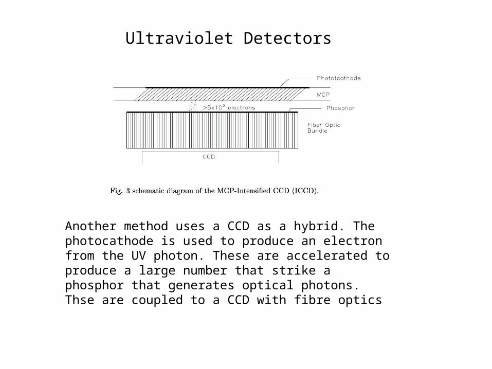
Another method uses a CCD as a hybrid. The photocathode is used to produce an electron from the UV photon. These are accelerated to produce a large number that strike a phosphor that generates optical photons. Thse are coupled to a CCD with fibre optics
Ultraviolet Detectors

X-ray CCD Detectors
CCDs can also be used for X-ray observations with some differences to optical CCDs:
• Optical CCDs produce one electron per photon. Many photons have to be detected before a measurable signal can be produced. A single X-ray photon can produce 100-1000 electrons (1 electron per 3.6 eV of energy). With low amplifier noise this can be measured. Thus X-ray CCDs are photon counting devices
• Requires one photon incident per pixel which means integration times of ~secs for most astronomical sources
• Lower CTE with losses of about 1%

The detector of the future: a photon counter that measures each photon, its time of arrival, and its energy. This will be a detector and spectrograph in one.