at25080b and at25160b - microchip...
TRANSCRIPT

AT25080B and AT25160B
SPI Serial EEPROMs
8K (1,024 x 8) and 16K (2,048 x 8)
DATASHEET
Features
Serial Peripheral Interface (SPI) Compatible
Supports SPI Modes 0 (0,0) and 3 (1,1)
Datasheet Describes Mode 0 Operation
Low-voltage and Standard-voltage Operation
1.8 (VCC = 1.8V to 5.5V)
20MHz Clock Rate (5V)
32-byte Page Mode
Block Write Protection
Protect 1/4, 1/2, or Entire Array
Write Protect (WP) Pin and Write Disable Instructions for Both Hardware and
Software Data Protection
Self-timed Write Cycle (5ms max)
High Reliability
Endurance: 1,000,000 Write Cycles
Data Retention: 100 Years
Green (Pb/Halide-free/RoHS Compliant) Packaging Options
Die Sales: Wafer Form, Tape and Reel, and Bumped Wafers
Description
The Atmel® AT25080B/160B provides 8,192/16,384 bits of Serial Electrically-
Erasable Programmable Read-Only Memory (EEPROM) organized as
1,024/2,048 words of 8 bits each. The device is optimized for use in many
industrial and commercial applications where low-power and low-voltage
operation are essential. The AT25080B/160B is available in space-saving 8-lead
JEDEC SOIC, 8-lead TSSOP, 8-pad UDFN, 8-pad XDFN, 8-ball VFBGA, and
8-ball WLCSP packages.
The AT25080B/160B is enabled through the Chip Select pin (CS) and accessed
via a 3-wire interface consisting of Serial Data Input (SI), Serial Data Output (SO),
and Serial Clock (SCK). All programming cycles are completely self-timed, and no
separate erase cycle is required before write.
Block Write protection is enabled by programming the status register with one of
four blocks of write protection. Separate program enable and program disable
instructions are provided for additional data protection. Hardware data protection
is provided via the WP pin to protect against inadvertent write attempts to the
status register. The HOLD pin may be used to suspend any serial communication
without resetting the serial sequence.
Atmel-5228G-SEEPROM-AT25080B-160B-Datasheet_012015
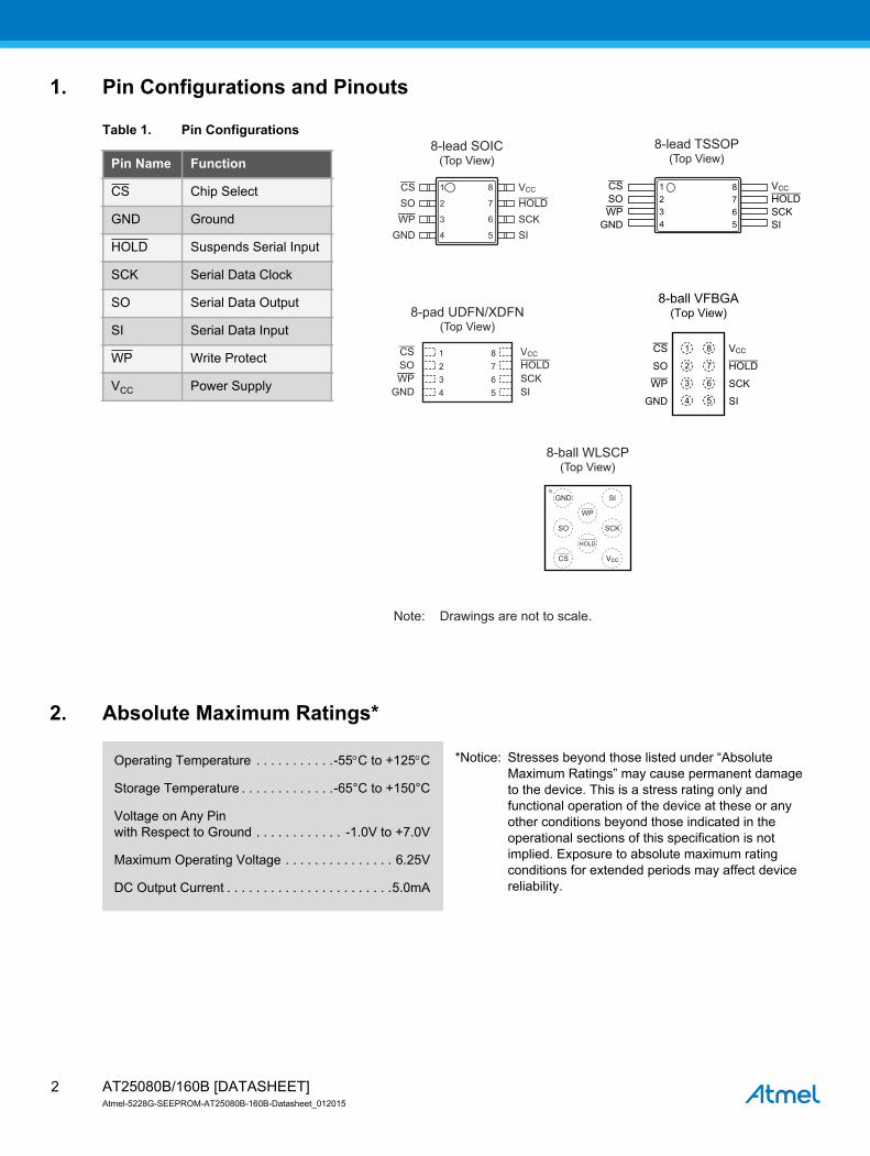
1. Pin Configurations and Pinouts
Table 1. Pin Configurations
2. Absolute Maximum Ratings*
Pin Name Function
CS Chip Select
GND Ground
HOLD Suspends Serial Input
SCK Serial Data Clock
SO Serial Data Output
SI Serial Data Input
WP Write Protect
VCC Power Supply
8-lead TSSOP(Top View)
1234
8765
CSSOWP
GND
VCCHOLDSCKSI
1
2
3
4
CSSOWP
GND
8
7
6
5
VCC
HOLDSCKSI
8-lead SOIC(Top View)
1234
CSSOWP
GND
8765
VCC
HOLDSCKSI
8-pad UDFN/XDFN(Top View)
CS
SO
WP
GND
VCC
HOLD
SCK
SI
1
2
3
4
8
7
6
5
8-ball VFBGA(Top View)
Note: Drawings are not to scale.
8-ball WLSCP(Top View)
GND SI
WP
SO SCK
HOLD
CS VCC
Operating Temperature . . . . . . . . . . .-55C to +125C
Storage Temperature . . . . . . . . . . . . .-65°C to +150°C
Voltage on Any Pin
with Respect to Ground . . . . . . . . . . . . -1.0V to +7.0V
Maximum Operating Voltage . . . . . . . . . . . . . . . 6.25V
DC Output Current . . . . . . . . . . . . . . . . . . . . . . .5.0mA
*Notice: Stresses beyond those listed under “Absolute
Maximum Ratings” may cause permanent damage
to the device. This is a stress rating only and
functional operation of the device at these or any
other conditions beyond those indicated in the
operational sections of this specification is not
implied. Exposure to absolute maximum rating
conditions for extended periods may affect device
reliability.
AT25080B/160B [DATASHEET]Atmel-5228G-SEEPROM-AT25080B-160B-Datasheet_012015
2
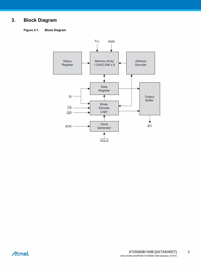
3. Block Diagram
Figure 3-1. Block Diagram
VCC GND
SI
SCK SO
StatusRegister
Memory Array1,024/2,048 x 8
AddressDecoder
DataRegister
OutputBuffer
ModeDecodeLogic
ClockGenerator
HOLD
CS
WP
3AT25080B/160B [DATASHEET]Atmel-5228G-SEEPROM-AT25080B-160B-Datasheet_012015
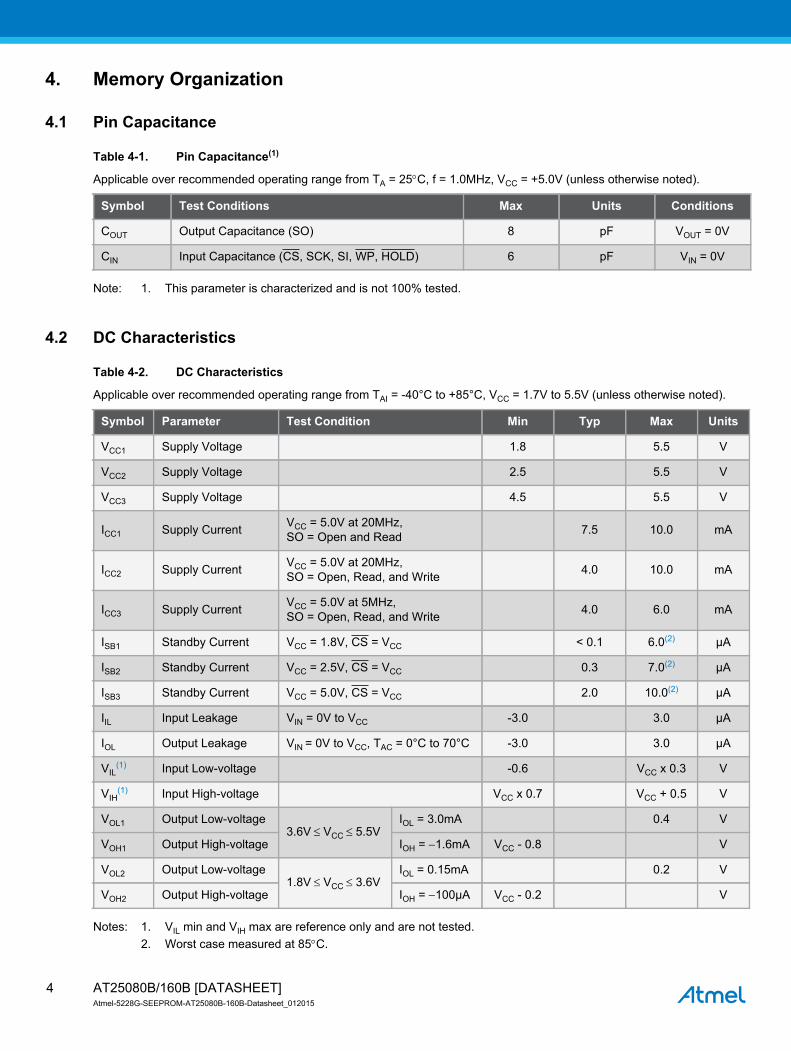
4. Memory Organization
4.1 Pin Capacitance
Table 4-1. Pin Capacitance(1)
Note: 1. This parameter is characterized and is not 100% tested.
4.2 DC Characteristics
Table 4-2. DC Characteristics
Notes: 1. VIL min and VIH max are reference only and are not tested.
2. Worst case measured at 85C.
Applicable over recommended operating range from TA = 25C, f = 1.0MHz, VCC = +5.0V (unless otherwise noted).
Symbol Test Conditions Max Units Conditions
COUT Output Capacitance (SO) 8 pF VOUT = 0V
CIN Input Capacitance (CS, SCK, SI, WP, HOLD) 6 pF VIN = 0V
Applicable over recommended operating range from TAI = -40°C to +85°C, VCC = 1.7V to 5.5V (unless otherwise noted).
Symbol Parameter Test Condition Min Typ Max Units
VCC1 Supply Voltage 1.8 5.5 V
VCC2 Supply Voltage 2.5 5.5 V
VCC3 Supply Voltage 4.5 5.5 V
ICC1 Supply CurrentVCC = 5.0V at 20MHz,
SO = Open and Read7.5 10.0 mA
ICC2 Supply CurrentVCC = 5.0V at 20MHz,
SO = Open, Read, and Write4.0 10.0 mA
ICC3 Supply CurrentVCC = 5.0V at 5MHz,
SO = Open, Read, and Write4.0 6.0 mA
ISB1 Standby Current VCC = 1.8V, CS = VCC < 0.1 6.0(2) μA
ISB2 Standby Current VCC = 2.5V, CS = VCC 0.3 7.0(2) μA
ISB3 Standby Current VCC = 5.0V, CS = VCC 2.0 10.0(2) μA
IIL Input Leakage VIN = 0V to VCC -3.0 3.0 μA
IOL Output Leakage VIN = 0V to VCC, TAC = 0°C to 70°C -3.0 3.0 μA
VIL(1) Input Low-voltage -0.6 VCC x 0.3 V
VIH(1) Input High-voltage VCC x 0.7 VCC + 0.5 V
VOL1 Output Low-voltage3.6V VCC 5.5V
IOL = 3.0mA 0.4 V
VOH1 Output High-voltage IOH = 1.6mA VCC - 0.8 V
VOL2 Output Low-voltage 1.8V VCC 3.6V
IOL = 0.15mA 0.2 V
VOH2 Output High-voltage IOH = 100μA VCC - 0.2 V
AT25080B/160B [DATASHEET]Atmel-5228G-SEEPROM-AT25080B-160B-Datasheet_012015
4
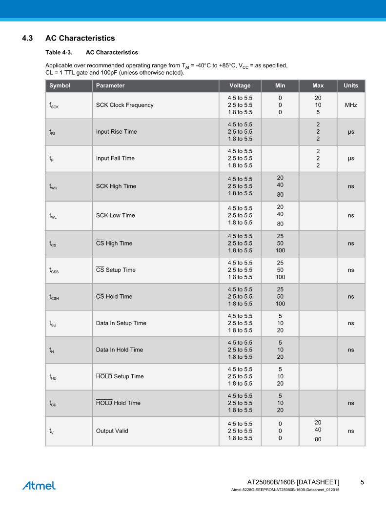
4.3 AC Characteristics
Table 4-3. AC Characteristics
Applicable over recommended operating range from TAI = -40C to +85C, VCC = as specified,
CL = 1 TTL gate and 100pF (unless otherwise noted).
Symbol Parameter Voltage Min Max Units
fSCK SCK Clock Frequency
4.5 to 5.5
2.5 to 5.5
1.8 to 5.5
0
0
0
20
10
5
MHz
tRI Input Rise Time
4.5 to 5.5
2.5 to 5.5
1.8 to 5.5
2
2
2
μs
tFI Input Fall Time
4.5 to 5.5
2.5 to 5.5
1.8 to 5.5
2
2
2
μs
tWH SCK High Time
4.5 to 5.5
2.5 to 5.5
1.8 to 5.5
20
40
80
ns
tWL SCK Low Time
4.5 to 5.5
2.5 to 5.5
1.8 to 5.5
20
40
80
ns
tCS CS High Time
4.5 to 5.5
2.5 to 5.5
1.8 to 5.5
25
50
100
ns
tCSS CS Setup Time
4.5 to 5.5
2.5 to 5.5
1.8 to 5.5
25
50
100
ns
tCSH CS Hold Time
4.5 to 5.5
2.5 to 5.5
1.8 to 5.5
25
50
100
ns
tSU Data In Setup Time
4.5 to 5.5
2.5 to 5.5
1.8 to 5.5
5
10
20
ns
tH Data In Hold Time
4.5 to 5.5
2.5 to 5.5
1.8 to 5.5
5
10
20
ns
tHD HOLD Setup Time
4.5 to 5.5
2.5 to 5.5
1.8 to 5.5
5
10
20
tCD HOLD Hold Time
4.5 to 5.5
2.5 to 5.5
1.8 to 5.5
5
10
20
ns
tV Output Valid
4.5 to 5.5
2.5 to 5.5
1.8 to 5.5
0
0
0
20
40
80
ns
5AT25080B/160B [DATASHEET]Atmel-5228G-SEEPROM-AT25080B-160B-Datasheet_012015
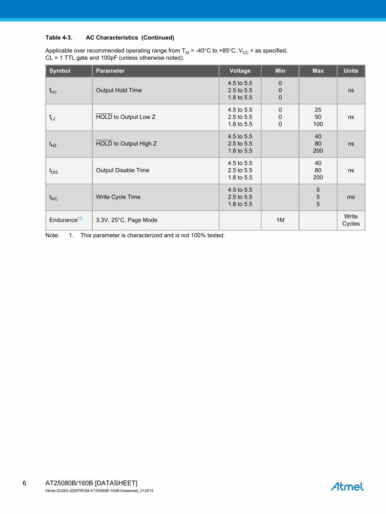
Note: 1. This parameter is characterized and is not 100% tested.
tHO Output Hold Time
4.5 to 5.5
2.5 to 5.5
1.8 to 5.5
0
0
0
ns
tLZ HOLD to Output Low Z
4.5 to 5.5
2.5 to 5.5
1.8 to 5.5
0
0
0
25
50
100
ns
tHZ HOLD to Output High Z
4.5 to 5.5
2.5 to 5.5
1.8 to 5.5
40
80
200
ns
tDIS Output Disable Time
4.5 to 5.5
2.5 to 5.5
1.8 to 5.5
40
80
200
ns
tWC Write Cycle Time
4.5 to 5.5
2.5 to 5.5
1.8 to 5.5
5
5
5
ms
Endurance(1) 3.3V, 25°C, Page Mode 1MWrite
Cycles
Table 4-3. AC Characteristics (Continued)
Applicable over recommended operating range from TAI = -40C to +85C, VCC = as specified,
CL = 1 TTL gate and 100pF (unless otherwise noted).
Symbol Parameter Voltage Min Max Units
AT25080B/160B [DATASHEET]Atmel-5228G-SEEPROM-AT25080B-160B-Datasheet_012015
6

5. Serial Interface Description
Table 5-1. Serial Interface Description
Interface Description
Master The device that generates the Serial Clock.
SlaveBecause the Serial Clock pin (SCK) is always an input, the AT25080B/160B always operates
as a slave.
Transmitter/ReceiverThe AT25080B/160B has separate pins designated for data transmission (SO) and
reception (SI).
MSB The Most Significant Bit (MSB) is the first bit transmitted and received.
Serial OpcodeAfter the device is selected with CS going low, the first byte will be received. This byte contains
the opcode that defines the operations to be performed.
Invalid Opcode
If an invalid opcode is received, no data will be shifted into the AT25080B/160B, and the serial
output pin (SO) will remain in a high-impedance state until the falling edge of CS is detected.
This will reinitialize the serial communication.
Chip Select
The AT25080B/160B is selected when the CS pin is low. When the device is not selected, data
will not be accepted via the SI pin, and the Serial Output pin (SO) will remain in a
high-impedance state.
Hold
The HOLD pin is used in conjunction with the CS pin to select the AT25080B/160B. When the
device is selected and a serial sequence is underway, Hold can be used to pause the serial
communication with the master device without resetting the serial sequence. To pause, the
HOLD pin must be brought low while the SCK pin is low. To resume serial communication, the
HOLD pin is brought high while the SCK pin is low (SCK may still toggle during Hold). Inputs to
the SI pin will be ignored while the SO pin is in the high impedance state.
Write Protect
The Write Protect pin (WP) allows normal Read and Write operations when held high. When
the WP pin is brought low and WPEN bit is one, all write operations to the status register are
inhibited. When the WP is low while CS is low, it will interrupt a Write to the status register. If
the internal write cycle has already been initiated, WP going low will have no effect on any
Write operation to the status register. The WP pin function is blocked when the WPEN bit in the
status register is zero. This will allow the user to install the AT25080B/160B in a system with
the WP pin tied to ground, and it will be able to write to the status register. All WP pin functions
are enabled when the WPEN bit is set to one.
7AT25080B/160B [DATASHEET]Atmel-5228G-SEEPROM-AT25080B-160B-Datasheet_012015

Figure 5-1. SPI Serial Interface
Master:Microcontroller
Slave:AT25080B/160B
Data Out (MOSI)
Data In (MISO)
Serial Clock (SPI CK)
SS0
SS1
SS2
SS3
SI
SO
SCK
CS
SI
SO
SCK
CS
SI
SO
SCK
CS
SI
SO
SCK
CS
AT25080B/160B [DATASHEET]Atmel-5228G-SEEPROM-AT25080B-160B-Datasheet_012015
8

6. Functional Description
The AT25080B/160B is designed to interface directly with the synchronous Serial Peripheral Interface (SPI) of
the 6805 and 68HC11 microcontroller series.
The AT25080B/160B utilizes an 8-bit instruction register. The list of instructions and their operation codes are
contained in the table below. All instructions, addresses, and data are transferred with the MSB first and starts
with a high-to-low CS transition.
Table 6-1. Instruction Set for the AT25080B/160B
Write Enable (WREN): The device will power up in the Write Disable state when VCC is applied. All
programming instructions must therefore be preceded by a Write Enable instruction.
Write Disable (WRDI): To protect the device against inadvertent writes, the WRDI instruction disables all
programming modes. The WRDI instruction is independent of the status of the WP pin.
Read Status Register (RDSR): The RDSR instruction provides access to the status register. The Ready/Busy
and Write Enable status of the device can be determined by the RDSR instruction. Similarly, the Block Write
Protection bits indicate the extent of protection employed. These bits are set by using the WRSR instruction.
Table 6-2. Status Register Format
Table 6-3. Read Status Register Bit Definition
Instruction Name Instruction Format Operation
WREN 0000 X110 Set Write Enable Latch
WRDI 0000 X100 Reset Write Enable Latch
RDSR 0000 X101 Read Status Register
WRSR 0000 X001 Write Status Register
Read 0000 X011 Read Data from Memory Array
Write 0000 X010 Write Data to Memory Array
Bit 7 Bit 6 Bit 5 Bit 4 Bit 3 Bit 2 Bit 1 Bit 0
WPEN X X X BP1 BP0 WEN RDY
Bit Definition
Bit 0 (RDY)If zero, it indicates the device is ready.
If one, it indicates the write cycle is in progress.
Bit 1 (WEN)If zero, it indicates the device is not write enabled.
If one, it indicates the device is write enabled.
Bit 2 (BP0) See Table 6-4 on page 10.
Bit 3 (BP1) See Table 6-4.
Bits 4 to 6 These are zeros when device is not in an internal write cycle.
Bit 7 (WPEN) See Table 6-5 on page 10
Bits 0 to 7 These are ones during an internal write cycle.
9AT25080B/160B [DATASHEET]Atmel-5228G-SEEPROM-AT25080B-160B-Datasheet_012015
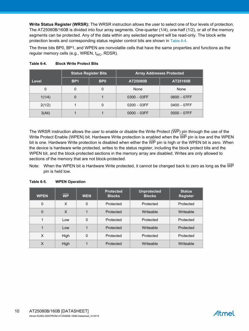
Write Status Register (WRSR): The WRSR instruction allows the user to select one of four levels of protection.
The AT25080B/160B is divided into four array segments. One-quarter (1/4), one-half (1/2), or all of the memory
segments can be protected. Any of the data within any selected segment will be read-only. The block write
protection levels and corresponding status register control bits are shown in Table 6-4.
The three bits BP0, BP1, and WPEN are nonvolatile cells that have the same properties and functions as the
regular memory cells (e.g., WREN, tWC, RDSR).
Table 6-4. Block Write Protect Bits
The WRSR instruction allows the user to enable or disable the Write Protect (WP) pin through the use of the
Write Protect Enable (WPEN) bit. Hardware Write protection is enabled when the WP pin is low and the WPEN
bit is one. Hardware Write protection is disabled when either the WP pin is high or the WPEN bit is zero. When
the device is hardware write protected, writes to the status register, including the block protect bits and the
WPEN bit, and the block-protected sections in the memory array are disabled. Writes are only allowed to
sections of the memory that are not block-protected.
Note: When the WPEN bit is Hardware Write protected, it cannot be changed back to zero as long as the WP
pin is held low.
Table 6-5. WPEN Operation
Level
Status Register Bits Array Addresses Protected
BP1 BP0 AT25080B AT25160B
0 0 0 None None
1(1/4) 0 1 0300 03FF 0600 07FF
2(1/2) 1 0 0200 03FF 0400 07FF
3(All) 1 1 0000 03FF 0000 07FF
WPEN WP WEN
Protected
Blocks
Unprotected
Blocks
Status
Register
0 X 0 Protected Protected Protected
0 X 1 Protected Writeable Writeable
1 Low 0 Protected Protected Protected
1 Low 1 Protected Writeable Protected
X High 0 Protected Protected Protected
X High 1 Protected Writeable Writeable
AT25080B/160B [DATASHEET]Atmel-5228G-SEEPROM-AT25080B-160B-Datasheet_012015
10
Read Sequence (Read): Reading the AT25080B/160B via the Serial Output (SO) pin requires the following
sequence. After the CS line is pulled low to select a device, the read opcode is transmitted via the SI line
followed by the byte address to be read (A15 to A0, see Table 6-6). Upon completion, any data on the SI line will
be ignored. The data (D7 to D0) at the specified address is then shifted out onto the SO line. If only one byte is
to be read, the CS line should be driven high after the data comes out. The read sequence can be continued
since the byte address is automatically incremented and data will continue to be shifted out. When the highest
address is reached, the address counter will roll-over to the lowest address allowing the entire memory to be
read in one continuous read cycle.
Write Sequence (Write): In order to program the AT25080B/160B, two separate instructions must be executed.
First, the device must be write enabled via the WREN instruction, and then a Write instruction can be
executed. The address of the memory location(s) to be programmed must be outside the protected address field
location selected by the block write protection level. During an internal write cycle, all commands will be ignored
except the RDSR instruction.
A Write instruction requires the following sequence. After the CS line is pulled low to select the device, the Write
opcode is transmitted via the SI line followed by the byte address (A15 to A0) and the data (D7 to D0) to be
programmed (see Table 6-6). Programming will start after the CS pin is brought high. The low-to-high transition
of the CS pin must occur during the SCK low-time immediately after clocking in the D0 (LSB) data bit.
The Ready/Busy status of the device can be determined by initiating a RDSR instruction. If Bit 0 is one, the write
cycle is still in progress. If Bit 0 is zero, the write cycle has ended. Only the RDSR instruction is enabled during
the write programming cycle.
The AT25080B/160B is capable of a 32-byte Page Write operation. After each byte of data is received, the five
low-order address bits are internally incremented by one; the high-order bits of the address will remain constant.
If more than 32 bytes of data are transmitted, the address counter will roll-over and the previously written data
will be overwritten. The AT25080B/160B is automatically returned to the write disable state at the completion of
a write cycle.
Note: If the device is not write-enabled (WREN), the device will ignore the Write instruction and will return to
the standby state when CS is brought high. A new CS falling edge is required to reinitiate the serial
communication.
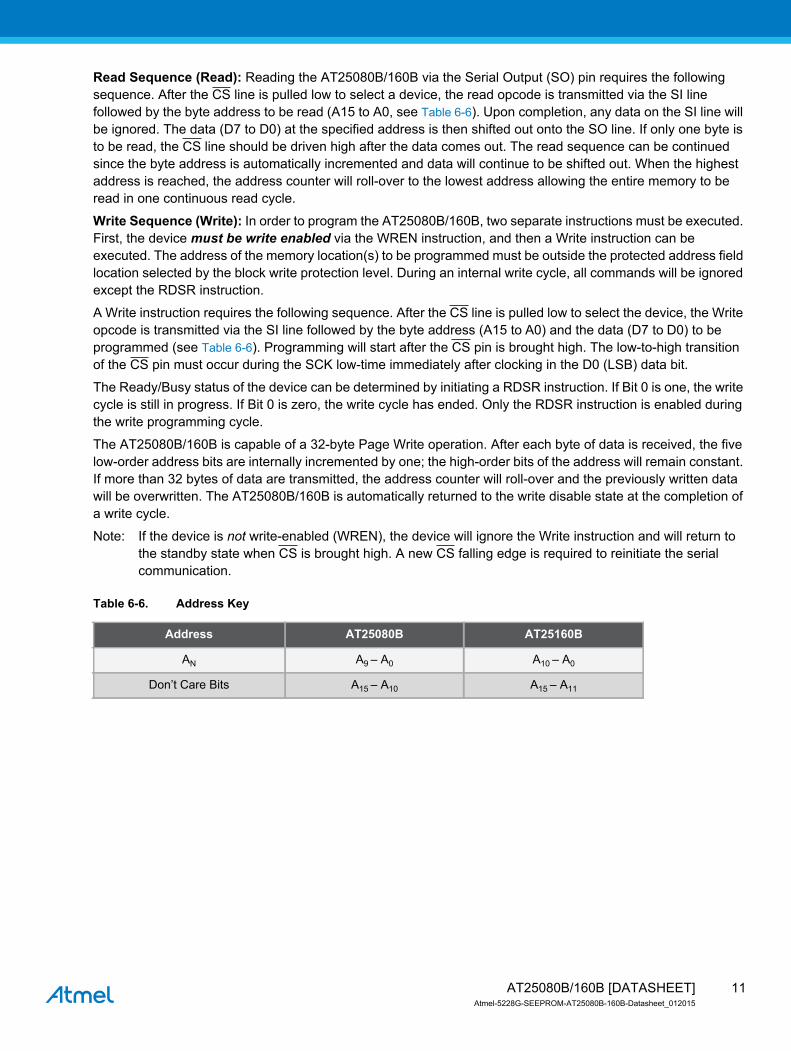
Table 6-6. Address Key
Address AT25080B AT25160B
AN A9 – A0 A10 – A0
Don’t Care Bits A15 – A10 A15 – A11
11AT25080B/160B [DATASHEET]Atmel-5228G-SEEPROM-AT25080B-160B-Datasheet_012015
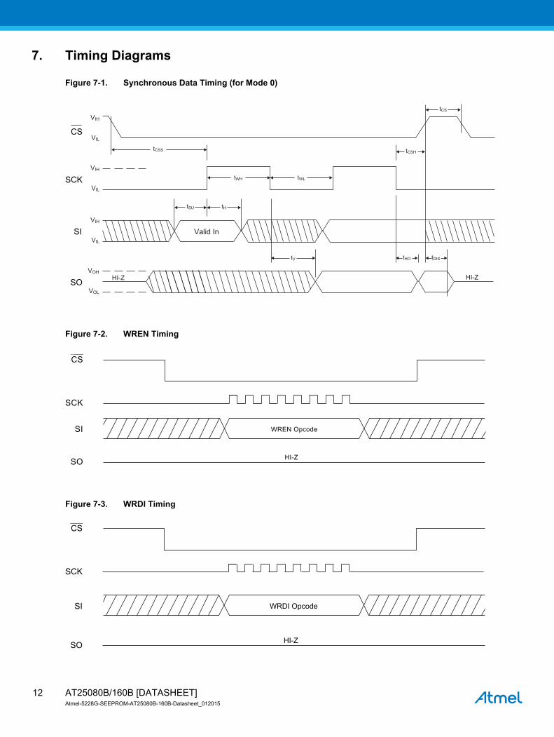
7. Timing Diagrams
Figure 7-1. Synchronous Data Timing (for Mode 0)
Figure 7-2. WREN Timing
Figure 7-3. WRDI Timing
tDIStHO
tCSH
tCS
tV
tH
VOH
VOL
HI-Z HI-Z
Valid In
tWH
VIH
VIH
VIL
tCSS
tWLSCK
SI
SO
CS
VIL
VIH
VIL
tSU
SO
SI
SCK
CS
WREN Opcode
HI-Z
SO
SI
SCK
CS
WRDI Opcode
HI-Z
AT25080B/160B [DATASHEET]Atmel-5228G-SEEPROM-AT25080B-160B-Datasheet_012015
12
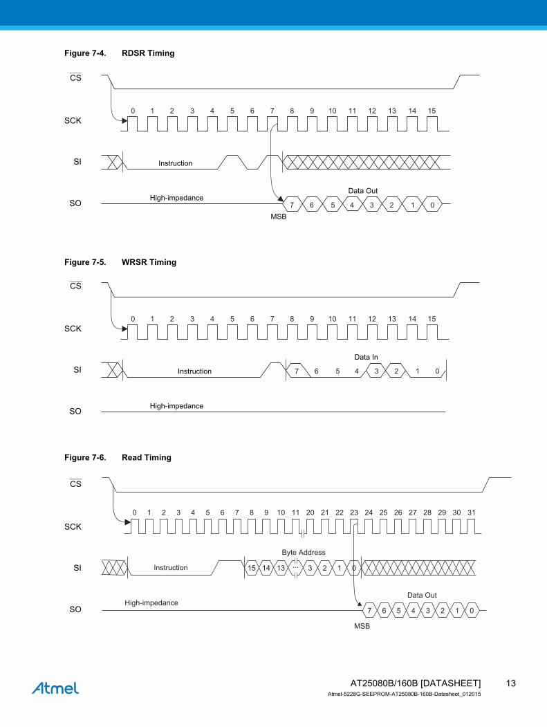
Figure 7-4. RDSR Timing
Figure 7-5. WRSR Timing
Figure 7-6. Read Timing
SO
SI
SCK
CS
0 1 2 3 4 5 6 7 8 9 10 11 12 13 14 15
Instruction
7 6 5 4 3 2 1 0
Data OutHigh-impedance
MSB
SO
SI
SCK
CS
0 1 2 3 4 5 6 7 8 9 10 11 12 13 14 15
Instruction
Data In
High-impedance
7 6 5 4 3 2 1 0
0
0
0
1
1
1
2
2
2
3
3
3
...
4
4
5
5
6
6
7
7
8 9 10
15 14 13
11 20 21 22 23 24 25 26 27 28 29 30
High-impedance
Instruction
Byte Address
MSB
Data Out
31
SO
SI
SCK
CS
13AT25080B/160B [DATASHEET]Atmel-5228G-SEEPROM-AT25080B-160B-Datasheet_012015
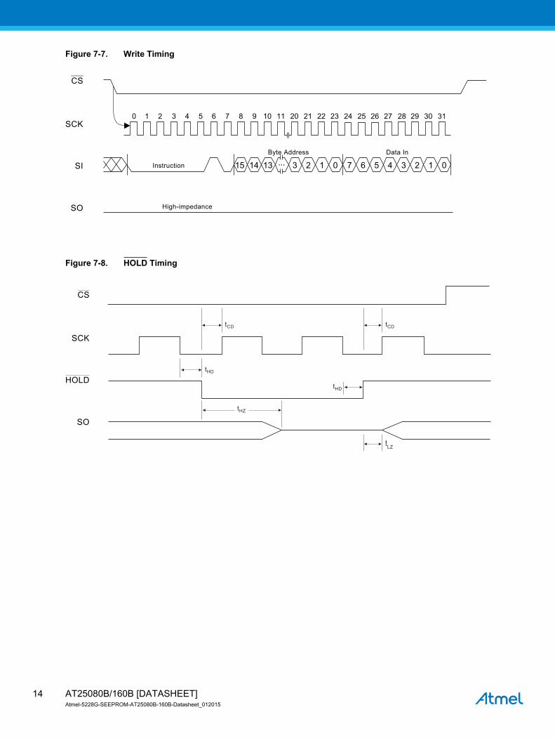
Figure 7-7. Write Timing
Figure 7-8. HOLD Timing
SO
SI
SCK
CS
0 1 2 3 4 5 6 7 8 9 10 11 20 21 22 23 24 25 26 27 28 29 30 31
Instruction
Byte Address Data In
High-impedance
7 6 5 4 3 2 1 015 14 13 ... 3 2 1 0
HOLD
SO
SCK
CS
tCD tCD
tHD
tHD
tLZ
tHZ
AT25080B/160B [DATASHEET]Atmel-5228G-SEEPROM-AT25080B-160B-Datasheet_012015
14
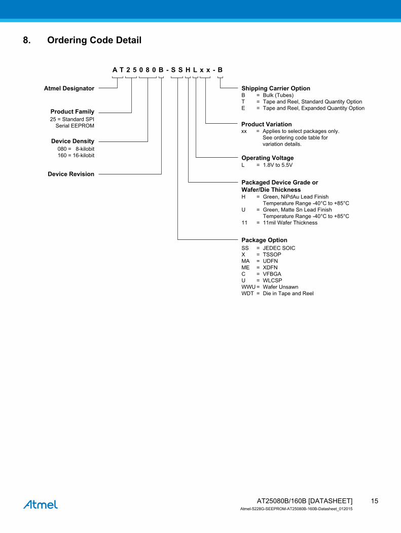
8. Ordering Code Detail
Atmel Designator
Product Family
Device Density
Device Revision
Shipping Carrier Option
Operating Voltage080 = 8-kilobit160 = 16-kilobit
B = Bulk (Tubes)T = Tape and Reel, Standard Quantity OptionE = Tape and Reel, Expanded Quantity Option
L = 1.8V to 5.5V
Packaged Device Grade orWafer/Die Thickness
Package Option
H = Green, NiPdAu Lead Finish Temperature Range -40°C to +85°CU = Green, Matte Sn Lead Finish Temperature Range -40°C to +85°C11 = 11mil Wafer Thickness
SS = JEDEC SOICX = TSSOPMA = UDFNME = XDFNC = VFBGAU = WLCSPWWU = Wafer UnsawnWDT = Die in Tape and Reel
Product Variationxx = Applies to select packages only. See ordering code table for variation details.
A T 2 5 0 8 0 B - S S H L x x - B
25 = Standard SPISerial EEPROM
15AT25080B/160B [DATASHEET]Atmel-5228G-SEEPROM-AT25080B-160B-Datasheet_012015
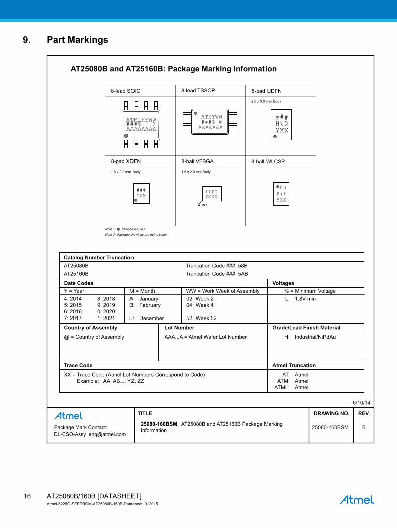
9. Part Markings
DRAWING NO. REV. TITLE
25080-160BSM B
6/10/14
25080-160BSM, AT25080B and AT25160B Package Marking Information Package Mark Contact:
AT25080B and AT25160B: Package Marking Information
Catalog Number Truncation AT25080B Truncation Code ###: 58BAT25160B Truncation Code ###: 5AB
Date Codes VoltagesY = Year M = Month WW = Work Week of Assembly % = Minimum Voltage 4: 2014 8: 2018 A: January 02: Week 2 L: 1.8V min5: 2015 9: 2019 B: February 04: Week 4 6: 2016 0: 2020 ... ... 7: 2017 1: 2021 L: December 52: Week 52
Country of Assembly Lot Number Grade/Lead Finish Material
@ = Country of Assembly AAA...A = Atmel Wafer Lot Number H: Industrial/NiPdAu
Trace Code Atmel Truncation
XX = Trace Code (Atmel Lot Numbers Correspond to Code) AT: Atmel Example: AA, AB.... YZ, ZZ ATM: Atmel ATML: Atmel
AAAAAAAA###% @ATMLHYWW
8-lead SOIC 8-lead TSSOP
AAAAAAA###% @ATHYWW
###YXX
8-pad XDFN
8-pad UDFN
###H%@YXX
2.0 x 3.0 mm Body
8-ball WLCSP
1.5 x 2.0 mm Body
8-ball VFBGA
PIN 1
###UYMXX
1.8 x 2.2 mm Body
Note 2: Package drawings are not to scale
Note 1: designates pin 1
@U###YXX
AT25080B/160B [DATASHEET]Atmel-5228G-SEEPROM-AT25080B-160B-Datasheet_012015
16

10. Ordering Information
Notes: 1. WLCSP Package:
This device includes a backside coating to increase product robustness.
CAUTION: Exposure to ultraviolet (UV) light can degrade the data stored in the EEPROM cells.
Therefore, customers who use a WLCSP product must ensure that exposure to ultraviolet light
does not occur.
2. Contact Atmel Sales for Wafer sales.
Atmel Ordering Code Lead Finish Package
Delivery InformationOperation
RangeForm Quantity
AT25080B-SSHL-B
NiPdAu
(Lead-free/Halogen-free)
8S1Bulk (Tubes) 100 per Tube
Industrial
Temperature
(-40 to 85C)
AT25080B-SSHL-T Tape and Reel 4,000 per Reel
AT25080B-XHL-B8X
Bulk (Tubes) 100 per Tube
AT25080B-XHL-T Tape and Reel 5,000 per Reel
AT25080B-MAHL-T8MA2
Tape and Reel 5,000 per Reel
AT25080B-MAHL-E Tape and Reel 15,000 per Reel
AT25080B-MEHL-T 8ME1 Tape and Reel 5,000 per Reel
AT25080B-CUL-T SnAgCu
(Lead-free/Halogen-free)
8U3-1 Tape and Reel 5,000 per Reel
AT25080B-UUL0B-T(1) 8U-12 Tape and Reel 5,000 per Reel
AT25080B-WWU11L(2) N/A Wafer Sale Note 2
AT25160B-SSHL-B
NiPdAu
(Lead-free/Halogen-free)
8S1Bulk (Tubes) 100 per Tube
Industrial
Temperature
(-40 to 85C)
AT25160B-SSHL-T Tape and Reel 4,000 per Reel
AT25160B-XHL-B8X
Bulk (Tubes) 100 per Tube
AT25160B-XHL-T Tape and Reel 5,000 per Reel
AT25160B-MAHL-T8MA2
Tape and Reel 5,000 per Reel
AT25160B-MAHL-E Tape and Reel 15,000 per Reel
AT25160B-MEHL-T 8ME1 Tape and Reel 5,000 per Reel
AT25160B-CUL-T SnAgCu
(Lead-free/Halogen-free)
8U3-1 Tape and Reel 5,000 per Reel
AT25160B-UUL0B-T(1) 8U-12 Tape and Reel 5,000 per Reel
AT25160B-WWU11L(2) N/A Wafer Sale Note 2
Package Type
8S1 8-lead, 0.150” wide, Plastic Gull Wing Small Outline (JEDEC SOIC)
8X 8-lead, 4.4mm body, Plastic Thin Shrink Small Outline Package (TSSOP)
8MA2 8-pad, 2.0mm x 3.0mm x 0.6mm body, Thermally Enhanced Plastic Ultra Thin Dual Flat Dual No Lead (UDFN)
8ME1 8-pad 1.8mm x 2.2mm body, Extra Thin DFN (XDFN)
8U3-1 8-ball, 1.50mm x 2.00mm body, 0.50mm pitch, Very Thin, Fine-Pitch Ball Grid Array (VFBGA)
8U-12 8-ball, 5 x 3 grid array, 0.40mm pitch, Wafer Level Chip Scale Package (WLCSP)
17AT25080B/160B [DATASHEET]Atmel-5228G-SEEPROM-AT25080B-160B-Datasheet_012015

11. Packaging Information
11.1 8S1 — 8-lead JEDEC SOIC
DRAWING NO. REV. TITLE GPC
COMMON DIMENSIONS(Unit of Measure = mm)
SYMBOL MIN NOM MAX NOTE
A1 0.10 – 0.25 A 1.35 – 1.75
b 0.31 – 0.51 C 0.17 – 0.25 D 4.80 – 5.05 E1 3.81 – 3.99 E 5.79 – 6.20 e 1.27 BSC L 0.40 – 1.27 ØØ 0° – 8°
Ø
E
1
N
TOP VIEW
C
E1
END VIEW
Ab
L
A1
e
D
SIDE VIEW
Package Drawing Contact:[email protected]
8S1 G
6/22/11
Notes: This drawing is for general information only. Refer to JEDEC Drawing MS-012, Variation AA for proper dimensions, tolerances, datums, etc.
8S1, 8-lead (0.150” Wide Body), Plastic Gull Wing Small Outline (JEDEC SOIC) SWB
AT25080B/160B [DATASHEET]Atmel-5228G-SEEPROM-AT25080B-160B-Datasheet_012015
18
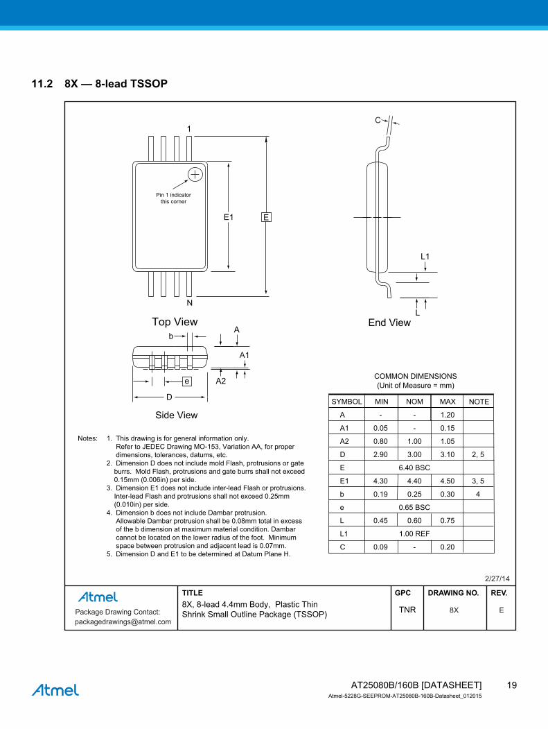
11.2 8X — 8-lead TSSOP
DRAWING NO. REV. TITLE GPC
COMMON DIMENSIONS(Unit of Measure = mm)
SYMBOL MIN NOM MAX NOTE
A - - 1.20
A1 0.05 - 0.15
A2 0.80 1.00 1.05
D 2.90 3.00 3.10 2, 5
E 6.40 BSC
E1 4.30 4.40 4.50 3, 5
b 0.19 0.25 0.30 4
e 0.65 BSC
L 0.45 0.60 0.75
L1 1.00 REF
C 0.09 - 0.20
Side View
End ViewTop View
A2
A
L
L1
D
1
E1
N
b
Pin 1 indicatorthis corner
E
e
Notes: 1. This drawing is for general information only. Refer to JEDEC Drawing MO-153, Variation AA, for proper dimensions, tolerances, datums, etc. 2. Dimension D does not include mold Flash, protrusions or gate burrs. Mold Flash, protrusions and gate burrs shall not exceed 0.15mm (0.006in) per side. 3. Dimension E1 does not include inter-lead Flash or protrusions. Inter-lead Flash and protrusions shall not exceed 0.25mm (0.010in) per side. 4. Dimension b does not include Dambar protrusion. Allowable Dambar protrusion shall be 0.08mm total in excess of the b dimension at maximum material condition. Dambar cannot be located on the lower radius of the foot. Minimum space between protrusion and adjacent lead is 0.07mm. 5. Dimension D and E1 to be determined at Datum Plane H.
Package Drawing Contact:[email protected]
8X E
2/27/14
8X, 8-lead 4.4mm Body, Plastic ThinShrink Small Outline Package (TSSOP) TNR
C
A1
19AT25080B/160B [DATASHEET]Atmel-5228G-SEEPROM-AT25080B-160B-Datasheet_012015
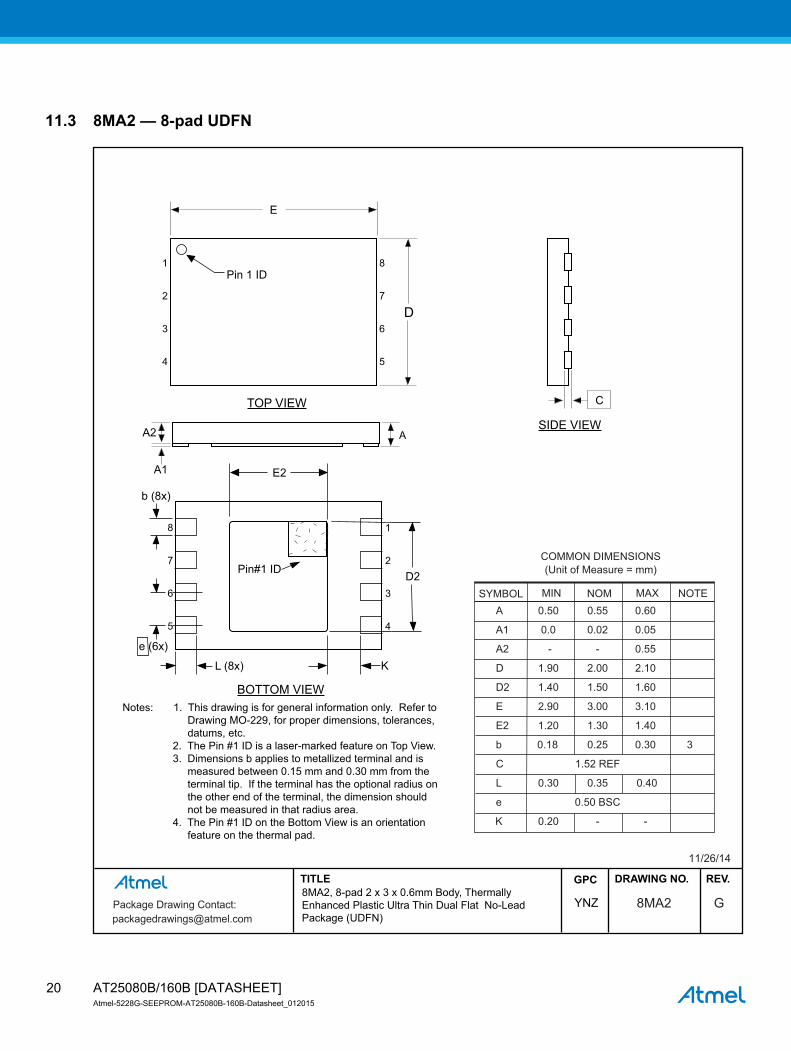
11.3 8MA2 — 8-pad UDFN
DRAWING NO. REV. TITLE GPC
8MA2 G
11/26/14
8MA2, 8-pad 2 x 3 x 0.6mm Body, ThermallyEnhanced Plastic Ultra Thin Dual Flat No-LeadPackage (UDFN)
YNZ
COMMON DIMENSIONS(Unit of Measure = mm)
SYMBOL MIN NOM MAX NOTE A 0.50 0.55 0.60
A1 0.0 0.02 0.05
A2 - - 0.55
D 1.90 2.00 2.10
D2 1.40 1.50 1.60
E 2.90 3.00 3.10
E2 1.20 1.30 1.40
b 0.18 0.25 0.30 3
C 1.52 REF
L 0.30 0.35 0.40
e 0.50 BSC
K 0.20 - -
TOP VIEW
SIDE VIEW
BOTTOM VIEW
Package Drawing Contact:[email protected]
C
E
Pin 1 ID
D
8
7
6
5
1
2
3
4
A
A1
A2
D2
E2
e (6x)
L (8x)
b (8x)
Pin#1 ID
K
1
2
3
4
8
7
6
5
Notes: 1. This drawing is for general information only. Refer to Drawing MO-229, for proper dimensions, tolerances, datums, etc. 2. The Pin #1 ID is a laser-marked feature on Top View. 3. Dimensions b applies to metallized terminal and is measured between 0.15 mm and 0.30 mm from the terminal tip. If the terminal has the optional radius on the other end of the terminal, the dimension should not be measured in that radius area. 4. The Pin #1 ID on the Bottom View is an orientation feature on the thermal pad.
AT25080B/160B [DATASHEET]Atmel-5228G-SEEPROM-AT25080B-160B-Datasheet_012015
20
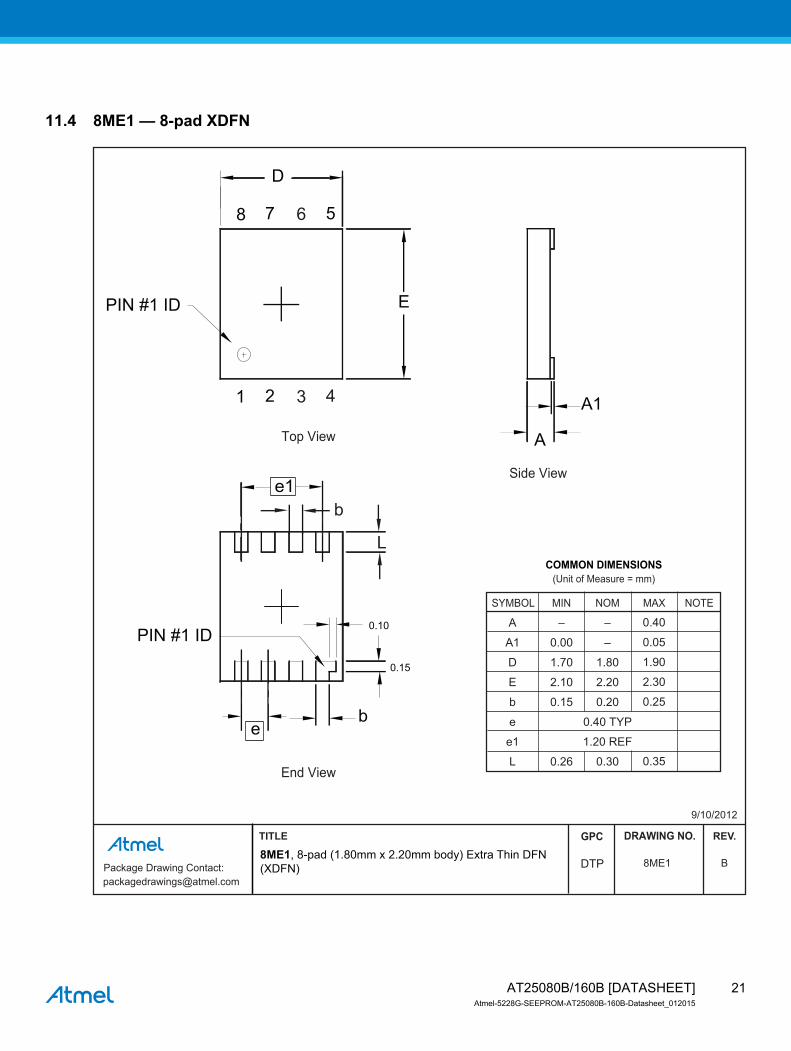
11.4 8ME1 — 8-pad XDFN
Package Drawing Contact:[email protected]
GPC DRAWING NO. REV. TITLE
COMMON DIMENSIONS(Unit of Measure = mm)
DTP
SYMBOL MIN NOM MAX NOTE
–
0.00
1.70
2.10
0.15
0.26
A
A1
D
E
b
e
e1
L
–
–
1.80
2.20
0.20
0.40 TYP
1.20 REF
0.30
0.40
0.05
1.90
2.30
0.25
0.35End View
8ME1 B
9/10/2012
8ME1, 8-pad (1.80mm x 2.20mm body) Extra Thin DFN (XDFN)
Top View
6 57
43
E
D
8
1 2
PIN #1 ID
0.10
0.15
b
L
b
e
PIN #1 ID
e1
A1
A
Side View
21AT25080B/160B [DATASHEET]Atmel-5228G-SEEPROM-AT25080B-160B-Datasheet_012015

11.5 8U3-1 — 8-ball VFBGA
DRAWING NO. REV. TITLE GPC
Package Drawing Contact:[email protected]
8U3-1 F
6/11/13
8U3-1, 8-ball, 1.50mm x 2.00mm body, 0.50mm pitch, Very Thin, Fine-Pitch Ball Grid Array Package (VFBGA) GXU
COMMON DIMENSIONS(Unit of Measure - mm)
SYMBOL MIN NOM MAX NOTE
A 0.73 0.79 0.85
A1 0.09 0.14 0.19
A2 0.40 0.45 0.50
b 0.20 0.25 0.30 2
D 1.50 BSC
E 2.0 BSC
e 0.50 BSC
e1 0.25 REF
d 1.00 BSC
d1 0.25 REF
1. This drawing is for general information only.
2. Dimension ‘b’ is measured at maximum solder ball diameter.
3. Solder ball composition shall be 95.5Sn-4.0Ag-.5Cu.
Notes:
A2
SIDE VIEW
A
PIN 1 BALL PAD CORNER
TOP VIEW
E
D
A1
b
8 SOLDER BALLSBOTTOM VIEW
(d1)
d
432
(e1)
6
e
57
PIN 1 BALL PAD CORNER1
8
2.
AT25080B/160B [DATASHEET]Atmel-5228G-SEEPROM-AT25080B-160B-Datasheet_012015
22
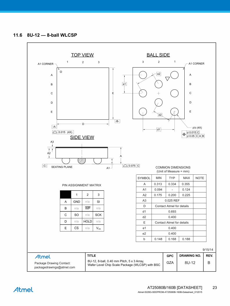
11.6 8U-12 — 8-ball WLCSP
DRAWING NO. REV. TITLE GPC
8U-12 B
9/15/14
8U-12, 8-ball, 0.40 mm Pitch, 5 x 3 Array, Wafer Level Chip Scale Package (WLCSP) with BSC
GZAPackage Drawing Contact:[email protected]
TOP VIEW
SIDE VIEW
BALL SIDE
d2
e2
E
e1
A2A
SEATING PLANE-C-A1
k 0.075 C
D
k 0.015 (4X)
E
-A-
D
C
B
A
-B-
db (4X)d1
d0.015 Cv
d0.05 C A B
E
D
C
B
A
2A1 CORNER1 3 A1 CORNER23 1
COMMON DIMENSIONS(Unit of Measure = mm)
SYMBOL MIN TYP MAX NOTE
A 0.313 0.334 0.355
A1 0.094 - 0.124
A2 0.175 0.200 0.225
A3 0.025 REF
D Contact Atmel for details
d1 0.693
d2 0.400
E Contact Atmel for details
e1 0.400
e2 0.400
b 0.148 0.168 0.188
PIN ASSIGNMENT MATRIX
A3
1 2
A
B
C
GND
WP
V
SCK
3
cc
n/a
n/an/a
n/a
n/a n/a
n/aCS
HOLD
SO
SI
D
E
23AT25080B/160B [DATASHEET]Atmel-5228G-SEEPROM-AT25080B-160B-Datasheet_012015
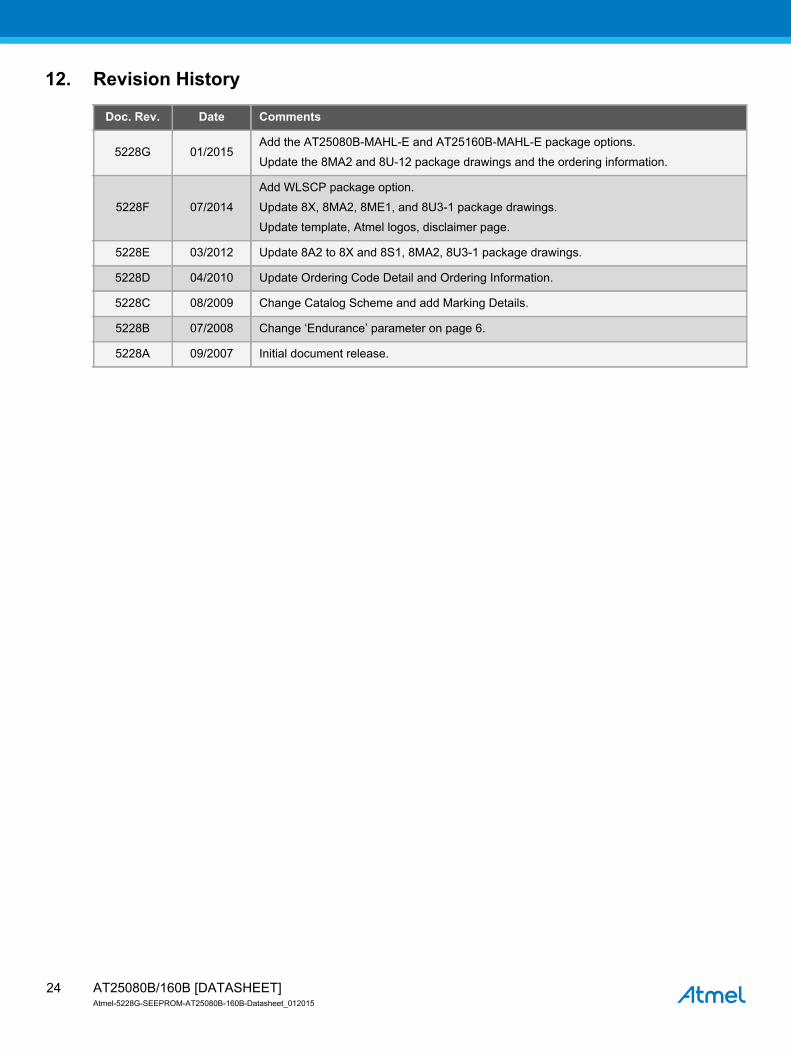
12. Revision History
Doc. Rev. Date Comments
5228G 01/2015Add the AT25080B-MAHL-E and AT25160B-MAHL-E package options.
Update the 8MA2 and 8U-12 package drawings and the ordering information.
5228F 07/2014
Add WLSCP package option.
Update 8X, 8MA2, 8ME1, and 8U3-1 package drawings.
Update template, Atmel logos, disclaimer page.
5228E 03/2012 Update 8A2 to 8X and 8S1, 8MA2, 8U3-1 package drawings.
5228D 04/2010 Update Ordering Code Detail and Ordering Information.
5228C 08/2009 Change Catalog Scheme and add Marking Details.
5228B 07/2008 Change ‘Endurance’ parameter on page 6.
5228A 09/2007 Initial document release.
AT25080B/160B [DATASHEET]Atmel-5228G-SEEPROM-AT25080B-160B-Datasheet_012015
24

XX X XX X
Atmel Corporation 1600 Technology Drive, San Jose, CA 95110 USA T: (+1)(408) 441.0311 F: (+1)(408) 436.4200 | www.atmel.com
© 2015 Atmel Corporation. / Rev.: Atmel-5228G-SEEPROM-AT25080B-160B-Datasheet_012015.
Atmel®, Atmel logo and combinations thereof, Enabling Unlimited Possibilities®, and others are registered trademarks or trademarks of Atmel Corporation in U.S. and other countries. Other terms and product names may be trademarks of others.
DISCLAIMER: The information in this document is provided in connection with Atmel products. No license, express or implied, by estoppel or otherwise, to any intellectual property rightis granted by this document or in connection with the sale of Atmel products. EXCEPT AS SET FORTH IN THE ATMEL TERMS AND CONDITIONS OF SALES LOCATED ON THEATMEL WEBSITE, ATMEL ASSUMES NO LIABILITY WHATSOEVER AND DISCLAIMS ANY EXPRESS, IMPLIED OR STATUTORY WARRANTY RELATING TO ITS PRODUCTSINCLUDING, BUT NOT LIMITED TO, THE IMPLIED WARRANTY OF MERCHANTABILITY, FITNESS FOR A PARTICULAR PURPOSE, OR NON-INFRINGEMENT. IN NO EVENTSHALL ATMEL BE LIABLE FOR ANY DIRECT, INDIRECT, CONSEQUENTIAL, PUNITIVE, SPECIAL OR INCIDENTAL DAMAGES (INCLUDING, WITHOUT LIMITATION, DAMAGESFOR LOSS AND PROFITS, BUSINESS INTERRUPTION, OR LOSS OF INFORMATION) ARISING OUT OF THE USE OR INABILITY TO USE THIS DOCUMENT, EVEN IF ATMEL HASBEEN ADVISED OF THE POSSIBILITY OF SUCH DAMAGES. Atmel makes no representations or warranties with respect to the accuracy or completeness of the contents of thisdocument and reserves the right to make changes to specifications and products descriptions at any time without notice. Atmel does not make any commitment to update the informationcontained herein. Unless specifically provided otherwise, Atmel products are not suitable for, and shall not be used in, automotive applications. Atmel products are not intended,authorized, or warranted for use as components in applications intended to support or sustain life.
SAFETY-CRITICAL, MILITARY, AND AUTOMOTIVE APPLICATIONS DISCLAIMER: Atmel products are not designed for and will not be used in connection with any applications wherethe failure of such products would reasonably be expected to result in significant personal injury or death (“Safety-Critical Applications”) without an Atmel officer's specific writtenconsent. Safety-Critical Applications include, without limitation, life support devices and systems, equipment or systems for the operation of nuclear facilities and weapons systems.Atmel products are not designed nor intended for use in military or aerospace applications or environments unless specifically designated by Atmel as military-grade. Atmel products arenot designed nor intended for use in automotive applications unless specifically designated by Atmel as automotive-grade.