atc113 training manual
TRANSCRIPT

8/12/2019 ATC113 Training Manual
http://slidepdf.com/reader/full/atc113-training-manual 1/13
1
0
10
1 0
1
0
1
1
01
0
10
1
0
1
0
1
0
10
1
0
1
0
1
0
1 0
0
1
0
1
RED OUTPUT
194V
TP50
TO
E8RED BIAS
<21-B>
E5003
E5007
TO
E7
GRN BIAS
0
1
1
0
0
0
0 1 11 0
VERTICAL
1
1
1
0
TP24
TECHNICAL TRAINING0
1
1
0
0
01
1
01
0
1
1
0
0
01
1
01
ATC113 TechnicalTraining Manual
VPORT

8/12/2019 ATC113 Training Manual
http://slidepdf.com/reader/full/atc113-training-manual 2/13
Page 1
Guide Plus+® is a registered trademark of Gemstar Development Corporation.
SAFETY INFORMATION
CAUTIONSafety information is contained in the appropriate Thomson multimedia Service Data. All product safety
requirements must be complied with prior to returning the instrument to the consumer. Servicers who
defeat safety features or fail to perform safety checks may be liable for any resulting damages and may
expose themselves and others to possible injury.
All integrated circuits, all surface mounted devices, and many other semi-
conductors are electrostatically sensitive and therefore require special
handling techniques.
First Edition - First Printing
Copyright 2002 Thomson multimedia Inc.
Trademark(s)® Registered Marca(s) Registrada(s)
Printed in U.S.A.
Prepared by
Thomson multimedia Inc.
Technical Training Department, INH905
PO Box 1976
Indianapolis, Indiana 46206 U.S.A.
This publication is intended to aid the technician in servicing the ATC113 television chassis. It will
explain the basic theory of operation. The manual covers power supply, Gem4 system control, and
YPrPb signal processing along with practical troubleshooting tips and suggestions. It is designed to
assist the technician in becoming familiar with chassis operation, increase confidence and improveoverall efficiency in servicing the product.
Note: This publication is intended to be used only as a training aid. It is not meant to replace service
data. TCE Electronic Service Information for this chassis contains specific information about parts,
safety and alignment procedures and must be consulted before performing any service. The informa-
tion in this manual is as accurate as possible at the time of publication. Circuit designs and drawings
are subject to change without notice.
FOREWORD

8/12/2019 ATC113 Training Manual
http://slidepdf.com/reader/full/atc113-training-manual 3/13
Page 2
Contents
FOREWORD ........................................................................................................ 1SAFETY INFORMATION CAUTION................................................................... 1
ATC113 INTRODUCTION ...................................................................................3ATC113 OVERVIEW............................................................................................4
GEMSTAR 4 AND SYSTEM CONTROL ............................................................6TROUBLESHOOTING THE GEM4 .................................................................... 7START-UP AND SHUTDOWN ............................................................................ 7
ATC113 Y PR PB PATH ...................................................................................... 8I/O MODULE TROUBLESHOOTING ................................................................8)
ATC113 POWER SUPPLY ..................................................................................9POWER SUPPLY OPERATION........................................................................10
KEY POINTS ABOUT THE ATC113 POWER SUPPLY .................................. 11POWER SUPPLY TROUBLESHOOTING TIPS ..............................................12

8/12/2019 ATC113 Training Manual
http://slidepdf.com/reader/full/atc113-training-manual 4/13
Page 3
ATC113 Introduction
Thomson’s latest TV chassis that will replace the CTC203 is the ATC113. This training
course will cover the ATC113 and its differences to the CTC203. First a general “Overview”
of key circuits of the ATC113 is covered followed by Gemstar 4 and troubleshooting the
GEM4. After the GEM4, this course will take the technician through the Y Pr Pb signal path
and I/O module troubleshooting followed by power supply and its operation. This course
ends with key points about the power supply and power supply troubleshooting tips. Upon
completion of this training course the service technician who is familiar with the CTC203
will be able to troubleshoot the ATC113 chassis.
The ATC113 is based on the CTC203 with minor changes. Aside from the obvious change
of the chassis numbering CTC to ATC, component numbering is the major change with
minor changes in the I/O and main chassis.
The changes that may or may not be covered in detail in this training course are:• All in one chip has changed to provide:
b. YPrPb inputs.
c. CRT Automatic Cut-Off Bias (ACB)d. Black level stretch.
e. 3.58 MHz output to synchronize a digital comb filter
f. Built-in horizontal oscillator without external resonator or alignment
g. Scan Velocity Modulation (SVM) output.• Audio amplifier is changed to increase audio power to 2 watts per channel.
• Audio BTSC stereo decoder IA01 is changed.
• Fly-back Transformer is changed to boost High Voltage by 1-2kV for improved
picture performance.
• ACRT driver IC is used to replace discrete components and improve video
performance.
In addition, the ATC113 has different I/O modules:I/O MODULE WITH V-PORT:
• This module will allow connection to the X-BOX via the 24-Way X-link cable, using
1H YPrPb and L/R signals from the X-BOX. Additional audio & video switch ICs will
be required to switch between X-BOX YPrPb and component YPrPb inputs.
I/O MODULE WITH PIP
• May or may not have V-Port connector.
I/O MODULE WITH COMB FILTER
• May or may not have PIP
BASIC I/O MODULE• No PIP or V-Port connector.
Audio and video switching IC (IY01) provides I2C bus communication and multi- A/V input
switching. All A/V switching is done on the I/O board.
The power supply and deflection circuits have stayed pretty much the same with only minor
changes.

8/12/2019 ATC113 Training Manual
http://slidepdf.com/reader/full/atc113-training-manual 5/13
Page 4
U26401
Gemstar 4
J 2 6 4 0 3
J 2 6 4 0 4
IV01Def. A/V
Processor
HorizontalOutputTL02
LL05IHVT
Vertical
OutputIF01
HYoke
V Yoke
AudioIA01
AudioOutput
IA03
EEPROMIR02
Stby I2C
EEPROMEnable
RGB
WBA
R/L Audio
Tuner
Video
IR out
FPA
Run I2C
OSD/FS
H/V Sync
IF
Run I2C
R/LAudTV
YPrPb Input
A/V Input
S-Video Input
Audio Input= CBA
= Chassis
PIP Tuner
IY03
IY01A/V
Sw
I/O & PIP CBA
6,7
34
38
14,15,16
4
ATC113 Overview
The ATC113 can be divided up into 3 main circuit areas: main chassis, Gemstar 4 module
and the I/O module. Major circuits on the main chassis are: Tuner, video processor,
horizontal output, vertical output, audio processing, audio output, and the EEPROM.
The main tuner processes NTSC RF signals and outputs IF to the video processor IV01
pins 6,7. TV Video is sent to the I/O for processing and is returned as Y Pr Pb from the IO
module. The Y Pr Pb signal is further processed by IV01 and output as RGB on pins 14,
15, and 16.
Audio comes out of IV01 as wide band audio on pin 4. The WBA signal is sent to IA01 for
processing into left and right audio signals. The audio processor decodes the stereo signal
and provides tone, volume, and balance adjustments to the audio signal. The audio
output is the final amp for speaker drive.
IV01 pin 34 is horizontal drive signal. This signal is further processed by the horizontal
output and used to drive the IHVT and the horizontal windings of the yoke.
Vertical output on pin 38 provides drive for the vertical output (IF01). IF01 is used to drivethe vertical windings of the yoke.
The EEPROM stores chassis alignment information and user settings. The alignments are
accessed using Chipper Check or front panel keys. Alignment and service menu access is
the same as the CTC203. For details on alignments, see the ATC113 ESI service data.

8/12/2019 ATC113 Training Manual
http://slidepdf.com/reader/full/atc113-training-manual 6/13
Page 5
There are three I2C busses in the ATC113 chassis, standby, run, and Gemstar. The
Standby bus is connected to the EEPROM (IR02). The Gemstar bus is internal to the
Gemstar module only and is used to communicate internal of the Gemstar module. The
run bus is connected to the remainder of the I2C devices: tuner, IV01, IA01, and I/O
module and provides communication throughout the chassis.
The Gemstar 4 module is the system control for the ATC113. It provides Gemstar guide
information processing and user input processing. The keyboard and IR commands are
processed by the Gemstar module and communicated to the chassis via I2C bus.
There are five I/O modules. Depending on inputs and features, these modules range from
a basic module with limited features to full feature module with PIP, V-port, and Y Pr Pb
inputs.
Most of the audio and video switching is done on the I/O by IY01. The comb/PIP processor
(IY03) provides PIP and Y/C switching / processing.

8/12/2019 ATC113 Training Manual
http://slidepdf.com/reader/full/atc113-training-manual 7/13

8/12/2019 ATC113 Training Manual
http://slidepdf.com/reader/full/atc113-training-manual 8/13
Page 7
Troubleshooting the Gem4
1. With AC power applied to the set.
2. Check BR104-14 for +5.2VE
3. Voltage incorrect or missing, troubleshoot STBY power supply4. Check BR103-10 and 12 (Clock & Data) for +5.0Vdc and 5Vp-p signal.
5. Signal present all the time troubleshoot main chassis and IR02.
6. Check BR104-4, 6, 8, and 10 for proper DC levels. Incorrect DC levels disconnect
BR202 and recheck.
7. Correct DC levels with BR202 disconnected troubleshoot keyboard.
8. Check for signal at BR104-12 and 13 when power button is pressed.
9. Clock and Data signal present when power is pressed troubleshoot the chassis.
10.Not present replace Gemstar module.
Start-up and Shutdown
3 Strikes and You’re Out ShutdownThe below error code table shows the different codes that can be thrown during the 3
strikes shutdown. The error codes can be viewed by accessing the service menu. Param-
eters 1, 2, and 3 are reserved for error codes. When viewing error codes for the first time it
is a good idea to reset all to zero and let the set go through the 3 strikes again. The new
error codes will indicate the first problem detected by the system control during start-up.
Error Code
(Dec) Device Condition
00 No error code thrown
03 U26401 Gemstar Micro 12V Run fault
08 IV01 XRP event detected
09 IV01 Power on reset
11 IY03 F2PIP Power on reset
12 IA01 Stereo Decoder Power on reset
16 U26401 Gemstar Micro Run I2C clock or data clamped at logic state 0
18 U26401 Gemstar Micro Stand-by I2C clock or data clamped at logic state 0
44 IY03 F2PIP No acknowledge from device
176 IA01 Stereo Decoder No acknowledge from device
180 3-Line Comb No acknowledge from device
144 IY01 A/V Switch No acknowledge from device
194 Tuner No acknowledge from device

8/12/2019 ATC113 Training Manual
http://slidepdf.com/reader/full/atc113-training-manual 9/13
Page 8
Buffer
26
4
5
GND
3
VCC
OUT
BIAS
1
IY07
Buffer
26
4
5
GND
3
VCC
OUT
BIAS
1
IY09
Buffer
26
4
5
GND
3
VCC
OUT
BIAS
1
IY08
IU01
I/O Board
Chassis
CRT Board
Y
Pr
PbR
G
B
XBoxConnector
Chassis
IV01
BY51
BV101
BY50
3233
16
XBox SW
47
43
44
14
15
16
ClockData
+5VE
Pb
Pr Pr
Pb Y
40 +9VE
IY01
Vcc
Yin
Yout
BY52
7 41
IY03 PIP
1
Y
ATC113 Y Pr Pb Path
The ATC113 is capable of two YPrPb inputs via conventional YPrPb cable and a special
cable connected to the V-Port (X-Box). Both inputs go three switch IC’s, IY09 for the Y
signal, IY07 for the Pr signal, and IY08 for the Pb signal. A voltage from the Gemstar
system control switches the three IC’s. BY51 pin 3 (XBOX SW) goes high approximately
3.1Vdc when the user selects V-Port input. When low, component input is selected. The Y
signal is further switched by IY01 (Audio / Video switch IC) and sent to the PIP processor or
comb filter. After PIP / Comb processing the Y signal along with Pr and Pb signals are sent
to connector BV101 and to the main chassis. All three signals are further processed by
IV01 and output as RGB to the CRT driver IU01.
I/O Module Troubleshooting
NOTE: Without the I/O module connected to the chassis the set will go through the 3-
strikes and you’re out shutdown.
The different I/O modules are board level troubleshooting. By checking the signals and
voltages to and from the I/O one can isolate down to board level. There are no set
procedures for this type of troubleshooting. Checking all signals and voltages on all
connectors is the only way to troubleshoot the I/O module. See service data for signal and
voltage requirements of each I/O.
8/12/2019 ATC113 Training Manual
http://slidepdf.com/reader/full/atc113-training-manual 10/13
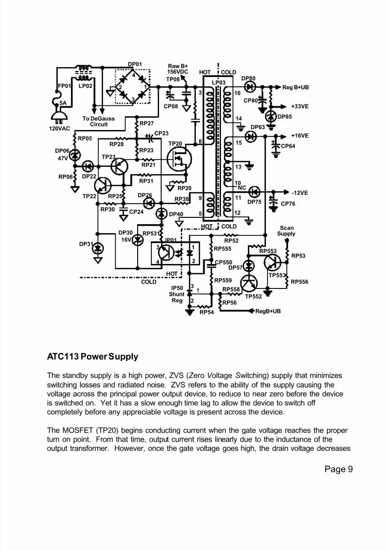
Page 9
13
4 2
HOT COLD
HOT
COLD
HOT COLD
LP03
IP01
156VDCRaw B+
3
2
1
120VAC
FP01
5A
TP08
TP20
TP23
TP22
DP06
47V
DP22
DP31
DP26
DP40
CP08
DP80
DP63
DP75
CP23
IP50
DP30
16V
To DeGaussCircuit
DP01
RP20
RP31
RP21
RP23
RP27
RP28
RP30
RP25RP38
5
9
8
3
RP531
RegB+UB
TP552
TP553
DP57
RP52
RP559
CP550
RP56
RP558
RP54
+16VE
RP555 RP553RP53
CP24
ScanSupply
16
14
15
13
10
11
12
NC
Reg B+UB
-12VE
LP02
ShuntReg
CP80
CP64
CP76
4
3
2 1
+33VE
RP556
RP05
RP06
DP85
ATC113 Power Supply
The standby supply is a high power, ZVS (Z ero V oltage S witching) supply that minimizes
switching losses and radiated noise. ZVS refers to the ability of the supply causing thevoltage across the principal power output device, to reduce to near zero before the device
is switched on. Yet it has a slow enough time lag to allow the device to switch off
completely before any appreciable voltage is present across the device.
The MOSFET (TP20) begins conducting current when the gate voltage reaches the proper
turn on point. From that time, output current rises linearly due to the inductance of the
output transformer. However, once the gate voltage goes high, the drain voltage decreases

8/12/2019 ATC113 Training Manual
http://slidepdf.com/reader/full/atc113-training-manual 11/13
Page 10
almost to zero volts. This eliminates much of the heat dissipation normally required of an
output device.
By reducing the switching losses to almost zero, the efficiency of the power supply is
greatly increased and the limiting of the switching voltages causes a substantial reduction
of switching noise.
Power Supply Operation
When AC is applied, DP01 converts the AC to approximately 156Vdc that is filtered by
CP08.
This “Raw B+” has two paths. First is through the transformer LP03 to the drain of TP20.
Second is through a series of resistors (RP27, 23, and 21) to the gate of TP20. As you
might guess this path is the start voltage for TP20.
With both drain and gate voltage TP20 conducts pulling the drain voltage to near zero,
collapsing the energy stored in LP03 winding pins 3, 8. This collapse causes voltage to beinduced into the secondary windings of LP03.
The winding on LP03 pins 9 and 5 is the secondary winding used for TP20 gate drive and
bias for TP22 and TP23. The pulse from this winding is sent to the anode and cathode of
DP26 and DP40 respectively. The positive bias is for the oscillator control circuit of TP22
and TP23. The negative bias is for IP01 and regulation. The un-rectified pulse provides
initial gate drive of TP20 via RP38, CP23, RP23, and RP21.
Oscillation occurs as TP20 turns on and off. TP22 and TP23 function as a latch circuit to
turn off TP20. As TP20 conducts, current is pulled through RP20. At some point the voltage
across RP20 increases till TP22 turns on. TP22 turns on pulling the base of TP23 lower turning on TP23. With TP23 on, TP20 is turned off removing the voltage developed across
RP20 turning off TP22 and so on. The re-supply pulse and B+ through RP27 start the cycle
all over again.
Feedback is used to control the on time of TP20. The longer TP20 stays on, the more
current is developed in LP03. There are two feedback paths from the secondary side, the
+16V and the REG B+. Both voltages are required for proper regulation and run of the
power supply. IP50 shunt regulator controls the voltage across IP01 pins 1 and 2. As Reg
B+ goes up, IP50 becomes more resistive or open turning off IP01.
IP01 is used to couple the secondary to the primary. As the transistor in IP01 turns on
more, the less negative pin 4 becomes. This causes DP20’s emitter voltage to be more
positive. A more positive voltage on the emitter of TP22 means that the base voltage needs
to be more positive for it to turn on, there for TP20 stays on longer.

8/12/2019 ATC113 Training Manual
http://slidepdf.com/reader/full/atc113-training-manual 12/13
Page 11
Key points about the ATC113 ZVS power supply:• Stand-by operating frequency of 60 to 65KHz.
• RP20 over current protection.• DP30 over voltage protection.• TP552 and TP553 used for run mode current increase.•
If TP20 fails replace all active components on primary side.• Run operating frequency of 40 to 50KHz.
13
4 2
HOT COLD
HOT
COLD
HOT COLD
LP03
IP01
156VDCRaw B+
3
2
1
120VAC
FP01
5A
TP08
TP20
TP23
TP22
DP06
47V
DP22
DP31
DP26
DP40
CP08
DP80
DP63
DP75
CP23
IP50
DP30
16V
To DeGaussCircuit
DP01
RP20
RP31
RP21
RP23
RP27
RP28
RP30
RP25RP38
5
9
8
3
RP531
RegB+UB
TP552
TP553
DP57
RP52
RP559
CP550
RP56
RP558
RP54
+16VE
RP555 RP553RP53
CP24
ScanSupply
16
14
15
13
10
11
12
NC
Reg B+UB
-12VE
LP02
ShuntReg
CP80
CP64
CP76
4
3
2 1
+33VE
RP556
RP05
RP06
DP85

8/12/2019 ATC113 Training Manual
http://slidepdf.com/reader/full/atc113-training-manual 13/13
Page 12
Power Supply Troubleshooting Tips
NOTE: Voltage readings taken at 90VAC input using a Vari-AC.
Regulation Problem:
IP01 (Photo-Coupler) can be by-passed by shorting pins 1 and 2 of IP01, and connecting a
10K potentiometer across pins 3 and 4. With the potentiometer set to 10K the Reg B+ is
aprox. +140Vdc. At 7.5K the Reg B+ was aprox. +100Vdc.
IP50 can also be checked with the same setup as in IP01. As the Reg B+ goes up IP50
conducts. Monitoring pin 3 of IP50 and with Reg B+ at +100Vdc pin 3 is aporx. +12.5Vdc.
As Reg B+ goes up IP50 will conduct and pin 3 will drop to +1.8Vdc. By using the 10K
potentiometer one can vary the Reg B+ and check all functions of feedback control.
Start-up Problem:
Unsolder the Drain of TP20 and turn on the Vari-AC. The gate voltage of TP20 should
measure +11.5Vdc. Anything less check for loads in the star-up circuit. Anything more
check for an open in OSC circuit and DP06 circuit.
Check for shorts on the secondary of LP03. Excessive load on the power supply will cause
it to shutdown and pulse.