atmega16m1/atmega32m1/atmega64m1/ …
TRANSCRIPT

This is a summary document. The complete document is available on the Atmel website at www.atmel.com.
ATmega16M1/ATmega32M1/ATmega64M1/ATmega32C1/ATmega64C1 Automotive
8-bit Microcontroller with 16K/32K/64K Bytes In-systemProgrammable Flash
SUMMARY DATASHEET
Features
● High performance, low power AVR® 8-bit microcontroller
● Advanced RISC architecture
● 131 powerful instructions - most single clock cycle execution● 32 8 general purpose working registers● Fully static operation● Up to 1MIPS throughput per MHz● On-chip 2-cycle multiplier
● Data and non-volatile program memory
● 16K/32K/64K bytes flash of in-system programmable program memory● Endurance: 10,000 write/erase cycles
● Optional boot code section with independent lock bits● In-system programming by on-chip boot program
● True read-while-write operation● 512/1024/2048 bytes of in-system programmable EEPROM
● Endurance: 100,000 write/erase cycles
● Programming lock for flash program and EEPROM data security
● 1024/2048/4096 bytes internal SRAM
● On chip debug interface (debugWIRE)
● CAN 2.0A/B with 6 message objects - ISO 16845 certified (1)
● LIN 2.1 and 1.3 controller or 8-Bit UART
● One 12-bit high speed PSC (power stage controller) (only ATmega16/32/64M1)
● Non overlapping inverted PWM output pins with flexible dead-time● Variable PWM duty cycle and frequency● Synchronous update of all PWM registers● Auto stop function for emergency event
● Peripheral features
● One 8-bit general purpose Timer/Counter with separate prescaler, compare mode and capture mode
● One 16-bit general purpose Timer/Counter with separate prescaler, compare mode and capture mode
1. See certification on Atmel® web site.
7647HS-AVR-01/15
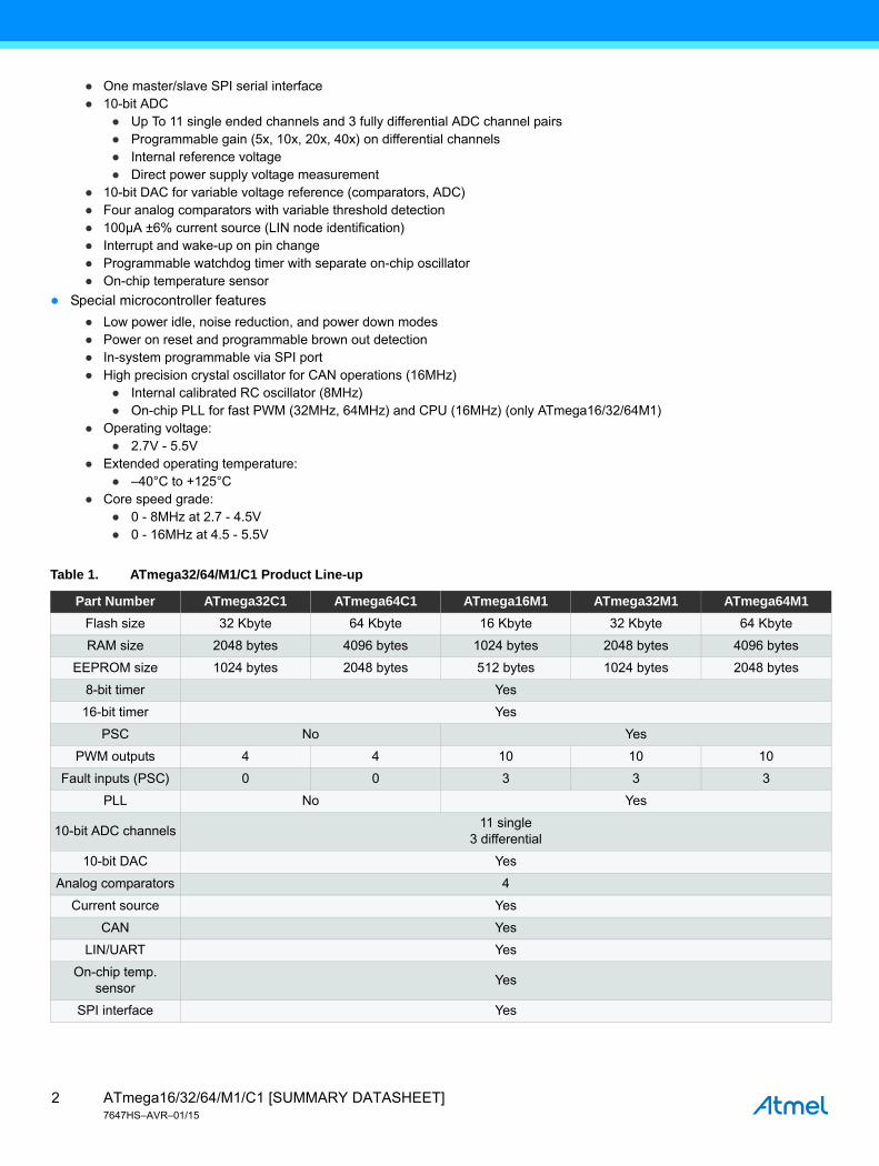
● One master/slave SPI serial interface● 10-bit ADC
● Up To 11 single ended channels and 3 fully differential ADC channel pairs● Programmable gain (5x, 10x, 20x, 40x) on differential channels● Internal reference voltage● Direct power supply voltage measurement
● 10-bit DAC for variable voltage reference (comparators, ADC)● Four analog comparators with variable threshold detection● 100µA ±6% current source (LIN node identification)● Interrupt and wake-up on pin change● Programmable watchdog timer with separate on-chip oscillator● On-chip temperature sensor
● Special microcontroller features
● Low power idle, noise reduction, and power down modes● Power on reset and programmable brown out detection● In-system programmable via SPI port● High precision crystal oscillator for CAN operations (16MHz)
● Internal calibrated RC oscillator (8MHz)● On-chip PLL for fast PWM (32MHz, 64MHz) and CPU (16MHz) (only ATmega16/32/64M1)
● Operating voltage:● 2.7V - 5.5V
● Extended operating temperature:● –40°C to +125°C
● Core speed grade:● 0 - 8MHz at 2.7 - 4.5V● 0 - 16MHz at 4.5 - 5.5V
Table 1. ATmega32/64/M1/C1 Product Line-up
Part Number ATmega32C1 ATmega64C1 ATmega16M1 ATmega32M1 ATmega64M1
Flash size 32 Kbyte 64 Kbyte 16 Kbyte 32 Kbyte 64 Kbyte
RAM size 2048 bytes 4096 bytes 1024 bytes 2048 bytes 4096 bytes
EEPROM size 1024 bytes 2048 bytes 512 bytes 1024 bytes 2048 bytes
8-bit timer Yes
16-bit timer Yes
PSC No Yes
PWM outputs 4 4 10 10 10
Fault inputs (PSC) 0 0 3 3 3
PLL No Yes
10-bit ADC channels11 single
3 differential
10-bit DAC Yes
Analog comparators 4
Current source Yes
CAN Yes
LIN/UART Yes
On-chip temp. sensor
Yes
SPI interface Yes
ATmega16/32/64/M1/C1 [SUMMARY DATASHEET]7647HS–AVR–01/15
2

1. Pin Configurations
Figure 1-1. ATmega16/32/64M1 TQFP32/QFN32 (7*7mm) Package
Note: On the engineering samples (parts marked AT90PWM324), the ACMPN3 alternate function is not located on PC4. It is located on PE2.
32 31 30 29 28 27 26 25
9 10 11 12 13 14 15 16
(PCINT18/PSCIN2/OC1A/MISO_A) PD2
(PCINT19/TXD/TXLIN/OC0A/SS/MOSI_A) PD3
(PCINT9/PSCIN1/OC1B/SS_A) PC1
(PCINT10/T0/TXCAN) PC2
(PCINT0/MISO/PSCOUT2A) PB0
(PCINT11/T1/RXCAN/ICP1B) PC3
PB4 (AMP0+/PCINT4)
PD
1 (P
CIN
T17/
PS
CIN
0/C
LKO
)
PE
0 (P
CIN
T24/
RE
SE
T/O
CD
)
PC
7 (D
2A/A
MP
2+/P
CIN
T15)
(PC
INT1
/MO
SI/P
SC
OU
T2B
) PB
1
(AC
MP
0/P
CIN
T23)
PD
7
(AD
C5/
INT1
/AC
MP
N0/
PC
INT2
) PB
2
(AD
C3/
AC
MP
N2/
INT0
/PC
INT2
2) P
D6
(AD
C2/
AC
MP
2/P
CIN
T21)
PD
5
(PC
INT2
0/A
DC
1/R
XD
/RX
LIN
/ICP
1A/S
CK
_A) P
D4
(PC
INT2
6/A
DC
0/X
TAL2
) PE
2
(PC
INT2
5/O
C0B
/XTA
L1) P
E1
PB
5 (A
DC
6/IN
T2/A
CM
PN
1/A
MP
2-/P
CIN
T5)
PB
6 (A
DC
7/P
SC
OU
T1B
/PC
INT6
)
PB
7 (A
DC
4/P
SC
OU
T0B
/SC
K/P
CIN
T7)
PD
0 (P
CIN
T16)
PC
0 (P
CIN
T8/IN
T3/P
SC
OU
T1A
)
PB3 (AMP0-/PCINT3)
PC6 (ADC10/ACMP1/PCINT14)
PC5 (ADC9/ACMP3/AMP1+/PCINT13)
PC4 (ADC8/ACMPN3/AMP1-/PCINT12)
AREF(ISRC)
AGND
AVCC
VCC
GND
1
2
3
4
5
6
7
8
24
23
22
21
20
19
18
17
3ATmega16/32/64/M1/C1 [SUMMARY DATASHEET]7647HS–AVR–01/15

Figure 1-2. ATmega32/64C1 TQFP32/QFN32 (7*7mm) Package
Note: On the first engineering samples (parts marked AT90PWM324), the ACMPN3 alternate function is not located on PC4. It is located on PE2.
32 31 30 29 28 27 26 25
9 10 11 12 13 14 15 16
(PCINT18/OC1A/MISO_A) PD2
(PCINT19/TXD/TXLIN/OC0A/SS/MOSI_A) PD3
(PCINT9/OC1B/SS_A) PC1
(PCINT10/T0/TXCAN) PC2
(PCINT0/MISO) PB0
(PCINT11/T1/RXCAN/ICP1B) PC3
PB4 (AMP0+/PCINT4)
PD
1 (P
CIN
T17/
CLK
O)
PE
0 (P
CIN
T24/
RE
SE
T/O
CD
)
PC
7 (D
2A/A
MP
2+/P
CIN
T15)
(PC
INT1
/MO
SI)
PB
1
(AC
MP
0/P
CIN
T23)
PD
7
(AD
C5/
INT1
/AC
MP
N0/
PC
INT2
) PB
2
(AD
C3/
AC
MP
N2/
INT0
/PC
INT2
2) P
D6
(AD
C2/
AC
MP
2/P
CIN
T21)
PD
5
(PC
INT2
0/A
DC
1/R
XD
/RX
LIN
/ICP
1A/S
CK
_A) P
D4
(PC
INT2
6/A
DC
0/X
TAL2
) PE
2
(PC
INT2
5/O
C0B
/XTA
L1) P
E1
PB
5 (A
DC
6/IN
T2/A
CM
PN
1/A
MP
2-/P
CIN
T5)
PB
6 (A
DC
7/P
CIN
T6)
PB
7 (A
DC
4/S
CK
/PC
INT7
)
PD
0 (P
CIN
T16)
PC
0 (P
CIN
T8/IN
T3)
PB3 (AMP0-/PCINT3)
PC6 (ADC10/ACMP1/PCINT14)
PC5 (ADC9/ACMP3/AMP1+/PCINT13)
PC4 (ADC8/ACMPN3/AMP1-/PCINT12)
AREF(ISRC)
AGND
AVCC
VCC
GND
1
2
3
4
5
6
7
8
24
23
22
21
20
19
18
17
ATmega16/32/64/M1/C1 [SUMMARY DATASHEET]7647HS–AVR–01/15
4

1.1 Pin Descriptions
: Table 1-1. Pin-out Description
QFN32 Pin Number Mnemonic Type Name, Function and Alternate Function
5 GND Power Ground: 0V reference
20 AGND Power Analog Ground: 0V reference for analog part
4 VCC Power Power supply
19 AVCC PowerAnalog Power Supply: This is the power supply voltage for analog part
For a normal use this pin must be connected.
21 AREF Power
Analog Reference: Reference for analog converter. This is the reference voltage of the A/D converter. As output, can be used by external analog
ISRC (Current Source Output)
8 PB0 I/O
MISO (SPI Master In Slave Out)
PSCOUT2A (PSC Module 2 Output A)
PCINT0 (Pin Change Interrupt 0)
9 PB1 I/O
MOSI (SPI Master Out Slave In)
PSCOUT2B (PSC Module 2 Output B)
PCINT1 (Pin Change Interrupt 1)
16 PB2 I/O
ADC5 (Analog Input Channel 5)
INT1 (External Interrupt 1 Input)
ACMPN0 (Analog Comparator 0 Negative Input)
PCINT2 (Pin Change Interrupt 2)
23 PB3 I/OAMP0- (Analog Differential Amplifier 0 Negative Input)
PCINT3 (Pin Change Interrupt 3)
24 PB4 I/OAMP0+ (Analog Differential Amplifier 0 Positive Input)
PCINT4 (Pin Change Interrupt 4)
26 PB5 I/O
ADC6 (Analog Input Channel 6)
INT2 (External Interrupt 2 Input)
ACMPN1 (Analog Comparator 1 Negative Input)
AMP2- (Analog Differential Amplifier 2 Negative Input)
PCINT5 (Pin Change Interrupt 5)
27 PB6 I/O
ADC7 (Analog Input Channel 7)
PSCOUT1B (PSC Module 1 Output A)
PCINT6 (Pin Change Interrupt 6)
28 PB7 I/O
ADC4 (Analog Input Channel 4)
PSCOUT0B (PSC Module 0 Output B)
SCK (SPI Clock)
PCINT7 (Pin Change Interrupt 7)
30 PC0 I/O
PSCOUT1A (PSC Module 1 Output A)
INT3 (External Interrupt 3 Input)
PCINT8 (Pin Change Interrupt 8)
Note: 1. On the first engineering samples (parts marked AT90PWM324), the ACMPN3 alternate function is not located on PC4. It is located on PE2.
5ATmega16/32/64/M1/C1 [SUMMARY DATASHEET]7647HS–AVR–01/15
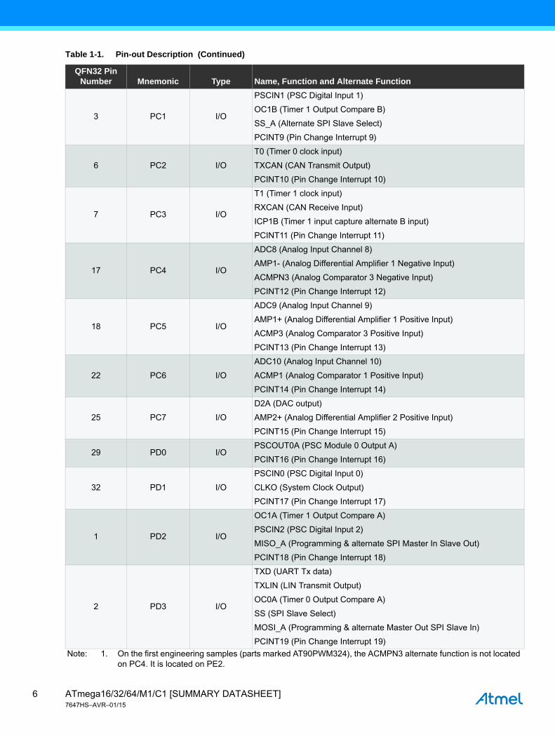
3 PC1 I/O
PSCIN1 (PSC Digital Input 1)
OC1B (Timer 1 Output Compare B)
SS_A (Alternate SPI Slave Select)
PCINT9 (Pin Change Interrupt 9)
6 PC2 I/O
T0 (Timer 0 clock input)
TXCAN (CAN Transmit Output)
PCINT10 (Pin Change Interrupt 10)
7 PC3 I/O
T1 (Timer 1 clock input)
RXCAN (CAN Receive Input)
ICP1B (Timer 1 input capture alternate B input)
PCINT11 (Pin Change Interrupt 11)
17 PC4 I/O
ADC8 (Analog Input Channel 8)
AMP1- (Analog Differential Amplifier 1 Negative Input)
ACMPN3 (Analog Comparator 3 Negative Input)
PCINT12 (Pin Change Interrupt 12)
18 PC5 I/O
ADC9 (Analog Input Channel 9)
AMP1+ (Analog Differential Amplifier 1 Positive Input)
ACMP3 (Analog Comparator 3 Positive Input)
PCINT13 (Pin Change Interrupt 13)
22 PC6 I/O
ADC10 (Analog Input Channel 10)
ACMP1 (Analog Comparator 1 Positive Input)
PCINT14 (Pin Change Interrupt 14)
25 PC7 I/O
D2A (DAC output)
AMP2+ (Analog Differential Amplifier 2 Positive Input)
PCINT15 (Pin Change Interrupt 15)
29 PD0 I/OPSCOUT0A (PSC Module 0 Output A)
PCINT16 (Pin Change Interrupt 16)
32 PD1 I/O
PSCIN0 (PSC Digital Input 0)
CLKO (System Clock Output)
PCINT17 (Pin Change Interrupt 17)
1 PD2 I/O
OC1A (Timer 1 Output Compare A)
PSCIN2 (PSC Digital Input 2)
MISO_A (Programming & alternate SPI Master In Slave Out)
PCINT18 (Pin Change Interrupt 18)
2 PD3 I/O
TXD (UART Tx data)
TXLIN (LIN Transmit Output)
OC0A (Timer 0 Output Compare A)
SS (SPI Slave Select)
MOSI_A (Programming & alternate Master Out SPI Slave In)
PCINT19 (Pin Change Interrupt 19)
Table 1-1. Pin-out Description (Continued)
QFN32 Pin Number Mnemonic Type Name, Function and Alternate Function
Note: 1. On the first engineering samples (parts marked AT90PWM324), the ACMPN3 alternate function is not located on PC4. It is located on PE2.
ATmega16/32/64/M1/C1 [SUMMARY DATASHEET]7647HS–AVR–01/15
6

12 PD4 I/O
ADC1 (Analog Input Channel 1)
RXD (UART Rx data)
RXLIN (LIN Receive Input)
ICP1A (Timer 1 input capture alternate A input)
SCK_A (Programming & alternate SPI Clock)
PCINT20 (Pin Change Interrupt 20)
13 PD5 I/O
ADC2 (Analog Input Channel 2)
ACMP2 (Analog Comparator 2 Positive Input)
PCINT21 (Pin Change Interrupt 21)
14 PD6 I/O
ADC3 (Analog Input Channel 3)
ACMPN2 (Analog Comparator 2 Negative Input)
INT0 (External Interrupt 0 Input)
PCINT22 (Pin Change Interrupt 22)
15 PD7 I/OACMP0 (Analog Comparator 0 Positive Input)
PCINT23 (Pin Change Interrupt 23)
31 PE0 I/O or I
RESET (Reset Input)
OCD (On Chip Debug I/O)
PCINT24 (Pin Change Interrupt 24)
10 PE1 I/O
XTAL1 (XTAL Input)
OC0B (Timer 0 Output Compare B)
PCINT25 (Pin Change Interrupt 25)
11 PE2 I/O
XTAL2 (XTAL Output)
ADC0 (Analog Input Channel 0)
PCINT26 (Pin Change Interrupt 26)
Table 1-1. Pin-out Description (Continued)
QFN32 Pin Number Mnemonic Type Name, Function and Alternate Function
Note: 1. On the first engineering samples (parts marked AT90PWM324), the ACMPN3 alternate function is not located on PC4. It is located on PE2.
7ATmega16/32/64/M1/C1 [SUMMARY DATASHEET]7647HS–AVR–01/15

2. Overview
The Atmel® ATmega16/32/64/M1/C1 is a low-power CMOS 8-bit microcontroller based on the AVR enhanced RISC architecture. By executing powerful instructions in a single clock cycle, the Atmel ATmega16/32/64/M1/C1 achieves throughputs approaching 1MIPS per MHz allowing the system designer to optimize power consumption versus processing speed.
2.1 Block Diagram
Figure 2-1. Block Diagram
The AVR® core combines a rich instruction set with 32 general purpose working registers. All the 32 registers are directly connected to the Arithmetic Logic Unit (ALU), allowing two independent registers to be accessed in one single instruction executed in one clock cycle. The resulting architecture is more code efficient while achieving throughputs up to ten times faster than conventional CISC microcontrollers.
Status andControl
InterruptUnit
32 x 8GeneralPurposeRegisters
ALU
Data Bus 8-bit
DataSRAM
SPIUnit
InstructionRegister
InstructionDecoder
WatchdogTimer
4 AnalogComparator
EEPROM
I/O Lines
Timer 1
Control Lines
Dire
ct A
ddre
ssin
g
Indi
rect
Add
ress
ing
Timer 0
HW LIN/UART
Currenr Source
ADC
CAN
MPSC
DAC
ProgramCounter
FlashProgramMemory
ATmega16/32/64/M1/C1 [SUMMARY DATASHEET]7647HS–AVR–01/15
8

The Atmel® ATmega16/32/64/M1/C1 provides the following features: 16K/32K/64K bytes of in-system programmable flash with read-while-write capabilities, 512/1024/2048 bytes EEPROM, 1024/2048/4096 bytes SRAM, 27 general purpose I/O lines, 32 general purpose working registers, one motor power stage controller, two flexible Timer/Counters with compare modes and PWM, one UART with HW LIN, an 11-channel 10-bit ADC with two differential input stages with programmable gain, a 10-bit DAC, a programmable watchdog timer with internal individual oscillator, an SPI serial port, an on-chip debug system and four software selectable power saving modes.
The idle mode stops the CPU while allowing the SRAM, Timer/Counters, SPI ports, CAN, LIN/UART and interrupt system to continue functioning. The power-down mode saves the register contents but freezes the oscillator, disabling all other chip functions until the next interrupt or hardware reset. The ADC noise reduction mode stops the CPU and all I/O modules except ADC, to minimize switching noise during ADC conversions. In standby mode, the crystal/resonator oscillator is running while the rest of the device is sleeping. This allows very fast start-up combined with low power consumption.
The device is manufactured using Atmel’s high-density nonvolatile memory technology. The on-chip ISP flash allows the program memory to be reprogrammed in-system through an SPI serial interface, by a conventional nonvolatile memory programmer, or by an on-chip boot program running on the AVR core. The boot program can use any interface to download the application program in the application flash memory. Software in the boot flash section will continue to run while the application flash section is updated, providing true read-while-write operation. By combining an 8-bit RISC CPU with in-system self-programmable flash on a monolithic chip, the Atmel ATmega16/32/64/M1/C1 is a powerful microcontroller that provides a highly flexible and cost effective solution to many embedded control applications.
The ATmega16/32/64/M1/C1 AVR® is supported with a full suite of program and system development tools including: C compilers, macro assemblers, program debugger/simulators, in-circuit emulators, and evaluation kits.
2.2 Automotive Quality Grade
The Atmel ATmega16/32/64/M1/C1 have been developed and manufactured according to the most stringent requirements of the international standard ISO-TS-16949. This data sheet contains limit values extracted from the results of extensive characterization (Temperature and Voltage). The quality and reliability of the ATmega16/32/64/M1/C1 have been verified during regular product qualification as per AEC-Q100 grade 1.
As indicated in the ordering information paragraph, the products are available in only one temperature grade.
2.3 Pin Descriptions
2.3.1 VCC
Digital supply voltage.
2.3.2 GND
Ground.
2.3.3 Port B (PB7..PB0)
Port B is an 8-bit bi-directional I/O port with internal pull-up resistors (selected for each bit). The port B output buffers have symmetrical drive characteristics with both high sink and source capability. As inputs, port B pins that are externally pulled low will source current if the pull-up resistors are activated. The port B pins are tri-stated when a reset condition becomes active, even if the clock is not running.
Port B also serves the functions of various special features of the ATmega16/32/64/M1/C1.
Table 2-1. Temperature Grade Identification for Automotive Products
Temperature Temperature Identifier Comments
–40°C; +125°C Z Full automotive temperature range
9ATmega16/32/64/M1/C1 [SUMMARY DATASHEET]7647HS–AVR–01/15

2.3.4 Port C (PC7..PC0)
Port C is an 8-bit bi-directional I/O port with internal pull-up resistors (selected for each bit). The port C output buffers have symmetrical drive characteristics with both high sink and source capability. As inputs, port C pins that are externally pulled low will source current if the pull-up resistors are activated. The port C pins are tri-stated when a reset condition becomes active, even if the clock is not running.
Port C also serves the functions of special features of the Atmel® ATmega16/32/64/M1/C1.
2.3.5 Port D (PD7..PD0)
Port D is an 8-bit bi-directional I/O port with internal pull-up resistors (selected for each bit). The port D output buffers have symmetrical drive characteristics with both high sink and source capability. As inputs, port D pins that are externally pulled low will source current if the pull-up resistors are activated. The port D pins are tri-stated when a reset condition becomes active, even if the clock is not running.
Port D also serves the functions of various special features of the Atmel ATmega16/32/64/M1/C1.
2.3.6 Port E (PE2..0) RESET/ XTAL1/ XTAL2
Port E is an 3-bit bi-directional I/O port with internal pull-up resistors (selected for each bit). The port E output buffers have symmetrical drive characteristics with both high sink and source capability. As inputs, port E pins that are externally pulled low will source current if the pull-up resistors are activated. The port E pins are tri-stated when a reset condition becomes active, even if the clock is not running.
If the RSTDISBL fuse is programmed, PE0 is used as an I/O pin. Note that the electrical characteristics of PE0 differ from those of the other pins of port E.
If the RSTDISBL fuse is unprogrammed, PE0 is used as a reset input. A low level on this pin for longer than the minimum pulse length will generate a reset, even if the clock is not running.
Depending on the clock selection fuse settings, PE1 can be used as input to the inverting oscillator amplifier and input to the internal clock operating circuit.
Depending on the clock selection fuse settings, PE2 can be used as output from the inverting oscillator amplifier.
2.3.7 AVCC
AVCC is the supply voltage pin for the A/D converter, D/A converter, current source. It should be externally connected to VCC, even if the ADC, DAC are not used. If the ADC is used, it should be connected to VCC through a low-pass filter.
2.3.8 AREF
This is the analog reference pin for the A/D converter.
2.4 About Code Examples
This documentation contains simple code examples that briefly show how to use various parts of the device. These code examples assume that the part specific header file is included before compilation. Be aware that not all C compiler vendors include bit definitions in the header files and interrupt handling in C is compiler dependent. Please confirm with the C compiler documentation for more details.
ATmega16/32/64/M1/C1 [SUMMARY DATASHEET]7647HS–AVR–01/15
10

3. Instruction Set Summary
Mnemonics Operands Description Operation Flags #Clocks
Arithmetic and Logic Instructions
ADD Rd, Rr Add two registers Rd Rd + Rr Z, C, N, V, H 1
ADC Rd, Rr Add with carry two registers Rd Rd + Rr + C Z, C, N, V, H 1
ADIW Rdl,K Add immediate to word Rdh:Rdl Rdh:Rdl + K Z, C, N, V, S 2
SUB Rd, Rr Subtract two registers Rd Rd – Rr Z, C, N, V, H 1
SUBI Rd, K Subtract constant from register Rd Rd – K Z, C, N, V, H 1
SBC Rd, Rr Subtract with carry two registers Rd Rd – Rr – C Z, C, N, V, H 1
SBCI Rd, K Subtract with carry constant from reg. Rd Rd – K – C Z, C, N, V, H 1
SBIW Rdl,K Subtract immediate from word Rdh:Rdl Rdh:Rdl – K Z, C, N, V, S 2
AND Rd, Rr Logical AND registers Rd Rd Rr Z, N, V 1
ANDI Rd, K Logical AND register and constant Rd Rd K Z, N, V 1
OR Rd, Rr Logical OR registers Rd Rd v Rr Z, N, V 1
ORI Rd, K Logical OR register and constant Rd Rd v K Z, N, V 1
EOR Rd, Rr Exclusive OR registers Rd Rd Rr Z, N, V 1
COM Rd One’s complement Rd 0xFF – Rd Z, C, N, V 1
NEG Rd Two’s complement Rd 0x00 – Rd Z, C, N, V, H 1
SBR Rd,K Set bit(s) in register Rd Rd v K Z, N, V 1
CBR Rd,K Clear bit(s) in register Rd Rd · (0xFF – K) Z, N, V 1
INC Rd Increment Rd Rd + 1 Z, N, V 1
DEC Rd Decrement Rd Rd – 1 Z, N, V 1
TST Rd Test for zero or minus Rd Rd Rd Z, N, V 1
CLR Rd Clear register Rd Rd Rd Z, N, V 1
SER Rd Set register Rd 0xFF None 1
MUL Rd, Rr Multiply unsigned R1:R0 Rd x Rr Z, C 2
MULS Rd, Rr Multiply signed R1:R0 Rd x Rr Z, C 2
MULSU Rd, Rr Multiply signed with unsigned R1:R0 Rd x Rr Z, C 2
FMUL Rd, Rr Fractional multiply unsigned R1:R0 (Rd x Rr) << 1 Z, C 2
FMULS Rd, Rr Fractional multiply signed R1:R0 (Rd x Rr) << 1 Z, C 2
FMULSU Rd, RrFractional multiply signed with
unsignedR1:R0 (Rd x Rr) << 1 Z, C 2
Branch Instructions
RJMP k Relative jump PC PC + k + 1 None 2
IJMP Indirect jump to (Z) PC Z None 2
JMP(*) k Direct jump PC k None 3
RCALL k Relative subroutine call PC PC + k + 1 None 3
ICALL Indirect call to (Z) PC Z None 3
CALL(*) k Direct subroutine call PC k None 4
RET Subroutine return PC STACK None 4
RETI Interrupt return PC STACK I 4
CPSE Rd,Rr Compare, skip if equal if (Rd = Rr) PC PC + 2 or 3 None 1/2/3
Note: 1. These Instructions are only available in “16K and 32K parts”
11ATmega16/32/64/M1/C1 [SUMMARY DATASHEET]7647HS–AVR–01/15
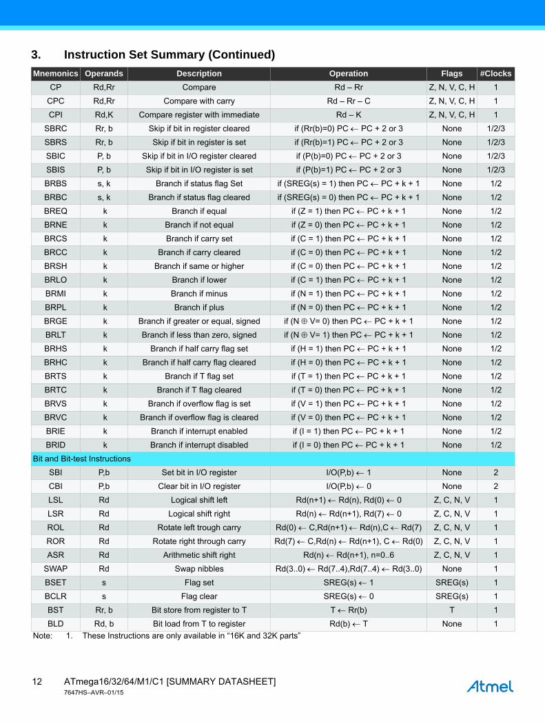
CP Rd,Rr Compare Rd – Rr Z, N, V, C, H 1
CPC Rd,Rr Compare with carry Rd – Rr – C Z, N, V, C, H 1
CPI Rd,K Compare register with immediate Rd – K Z, N, V, C, H 1
SBRC Rr, b Skip if bit in register cleared if (Rr(b)=0) PC PC + 2 or 3 None 1/2/3
SBRS Rr, b Skip if bit in register is set if (Rr(b)=1) PC PC + 2 or 3 None 1/2/3
SBIC P, b Skip if bit in I/O register cleared if (P(b)=0) PC PC + 2 or 3 None 1/2/3
SBIS P, b Skip if bit in I/O register is set if (P(b)=1) PC PC + 2 or 3 None 1/2/3
BRBS s, k Branch if status flag Set if (SREG(s) = 1) then PC PC + k + 1 None 1/2
BRBC s, k Branch if status flag cleared if (SREG(s) = 0) then PC PC + k + 1 None 1/2
BREQ k Branch if equal if (Z = 1) then PC PC + k + 1 None 1/2
BRNE k Branch if not equal if (Z = 0) then PC PC + k + 1 None 1/2
BRCS k Branch if carry set if (C = 1) then PC PC + k + 1 None 1/2
BRCC k Branch if carry cleared if (C = 0) then PC PC + k + 1 None 1/2
BRSH k Branch if same or higher if (C = 0) then PC PC + k + 1 None 1/2
BRLO k Branch if lower if (C = 1) then PC PC + k + 1 None 1/2
BRMI k Branch if minus if (N = 1) then PC PC + k + 1 None 1/2
BRPL k Branch if plus if (N = 0) then PC PC + k + 1 None 1/2
BRGE k Branch if greater or equal, signed if (N V= 0) then PC PC + k + 1 None 1/2
BRLT k Branch if less than zero, signed if (N V= 1) then PC PC + k + 1 None 1/2
BRHS k Branch if half carry flag set if (H = 1) then PC PC + k + 1 None 1/2
BRHC k Branch if half carry flag cleared if (H = 0) then PC PC + k + 1 None 1/2
BRTS k Branch if T flag set if (T = 1) then PC PC + k + 1 None 1/2
BRTC k Branch if T flag cleared if (T = 0) then PC PC + k + 1 None 1/2
BRVS k Branch if overflow flag is set if (V = 1) then PC PC + k + 1 None 1/2
BRVC k Branch if overflow flag is cleared if (V = 0) then PC PC + k + 1 None 1/2
BRIE k Branch if interrupt enabled if (I = 1) then PC PC + k + 1 None 1/2
BRID k Branch if interrupt disabled if (I = 0) then PC PC + k + 1 None 1/2
Bit and Bit-test Instructions
SBI P,b Set bit in I/O register I/O(P,b) 1 None 2
CBI P,b Clear bit in I/O register I/O(P,b) 0 None 2
LSL Rd Logical shift left Rd(n+1) Rd(n), Rd(0) 0 Z, C, N, V 1
LSR Rd Logical shift right Rd(n) Rd(n+1), Rd(7) 0 Z, C, N, V 1
ROL Rd Rotate left trough carry Rd(0) C,Rd(n+1) Rd(n),C Rd(7) Z, C, N, V 1
ROR Rd Rotate right through carry Rd(7) C,Rd(n) Rd(n+1), C Rd(0) Z, C, N, V 1
ASR Rd Arithmetic shift right Rd(n) Rd(n+1), n=0..6 Z, C, N, V 1
SWAP Rd Swap nibbles Rd(3..0) Rd(7..4),Rd(7..4) Rd(3..0) None 1
BSET s Flag set SREG(s) 1 SREG(s) 1
BCLR s Flag clear SREG(s) 0 SREG(s) 1
BST Rr, b Bit store from register to T T Rr(b) T 1
BLD Rd, b Bit load from T to register Rd(b) T None 1
3. Instruction Set Summary (Continued)
Mnemonics Operands Description Operation Flags #Clocks
Note: 1. These Instructions are only available in “16K and 32K parts”
ATmega16/32/64/M1/C1 [SUMMARY DATASHEET]7647HS–AVR–01/15
12

SEC Set carry C 1 C 1
CLC Clear carry C 0 C 1
SEN Set negative flag N 1 N 1
CLN Clear negative flag N 0 N 1
SEZ Set zero flag Z 1 Z 1
CLZ Clear zero flag Z 0 Z 1
SEI Global interrupt enable I 1 I 1
CLI Global interrupt disable I 0 I 1
SES Set signed test flag S 1 S 1
CLS Clear signed test flag S 0 S 1
SEV Set twos complement overflow. V 1 V 1
CLV Clear twos complement overflow V 0 V 1
SET Set T in SREG T 1 T 1
CLT Clear T in SREG T 0 T 1
SEH Set half carry flag in SREG H 1 H 1
CLH Clear half carry flag in SREG H 0 H 1
Data Transfer Instructions
MOV Rd, Rr Move between registers Rd Rr None 1
MOVW Rd, Rr Copy register word Rd+1:Rd Rr+1:Rr None 1
LDI Rd, K Load immediate Rd K None 1
LD Rd, X Load indirect Rd (X) None 2
LD Rd, X+ Load indirect and post-inc. Rd (X), X X + 1 None 2
LD Rd, – X Load indirect and pre-dec. X X – 1, Rd (X) None 2
LD Rd, Y Load indirect Rd (Y) None 2
LD Rd, Y+ Load indirect and post-inc. Rd (Y), Y Y + 1 None 2
LD Rd, – Y Load indirect and pre-dec. Y Y – 1, Rd (Y) None 2
LDD Rd,Y+q Load indirect with displacement Rd (Y + q) None 2
LD Rd, Z Load indirect Rd (Z) None 2
LD Rd, Z+ Load indirect and post-inc. Rd (Z), Z Z+1 None 2
LD Rd, –Z Load indirect and pre-dec. Z Z – 1, Rd (Z) None 2
LDD Rd, Z+q Load indirect with displacement Rd (Z + q) None 2
LDS Rd, k Load direct from SRAM Rd (k) None 2
ST X, Rr Store indirect (X) Rr None 2
ST X+, Rr Store indirect and post-inc. (X) Rr, X X + 1 None 2
ST – X, Rr Store indirect and pre-dec. X X – 1, (X) Rr None 2
ST Y, Rr Store indirect (Y) Rr None 2
ST Y+, Rr Store indirect and post-inc. (Y) Rr, Y Y + 1 None 2
ST – Y, Rr Store indirect and pre-dec. Y Y – 1, (Y) Rr None 2
STD Y+q,Rr Store indirect with displacement (Y + q) Rr None 2
ST Z, Rr Store indirect (Z) Rr None 2
3. Instruction Set Summary (Continued)
Mnemonics Operands Description Operation Flags #Clocks
Note: 1. These Instructions are only available in “16K and 32K parts”
13ATmega16/32/64/M1/C1 [SUMMARY DATASHEET]7647HS–AVR–01/15
ST Z+, Rr Store indirect and post-inc. (Z) Rr, Z Z + 1 None 2
ST –Z, Rr Store indirect and pre-dec. Z Z – 1, (Z) Rr None 2
STD Z+q,Rr Store indirect with displacement (Z + q) Rr None 2
STS k, Rr Store direct to SRAM (k) Rr None 2
LPM Load program memory R0 (Z) None 3
LPM Rd, Z Load program memory Rd (Z) None 3
LPM Rd, Z+ Load program memory and post-inc Rd (Z), Z Z+1 None 3
SPM Store program memory (Z) R1:R0 None -
IN Rd, P In port Rd P None 1
OUT P, Rr Out port P Rr None 1
PUSH Rr Push register on stack STACK Rr None 2
POP Rd Pop register from stack Rd STACK None 2
MCU Control Instructions
NOP No operation None 1
SLEEP Sleep (see specific descr. for sleep function) None 1
WDR Watchdog reset (see specific descr. for WDR/timer) None 1
BREAK Break For on-chip debug Only None N/A
3. Instruction Set Summary (Continued)
Mnemonics Operands Description Operation Flags #Clocks
Note: 1. These Instructions are only available in “16K and 32K parts”
ATmega16/32/64/M1/C1 [SUMMARY DATASHEET]7647HS–AVR–01/15
14
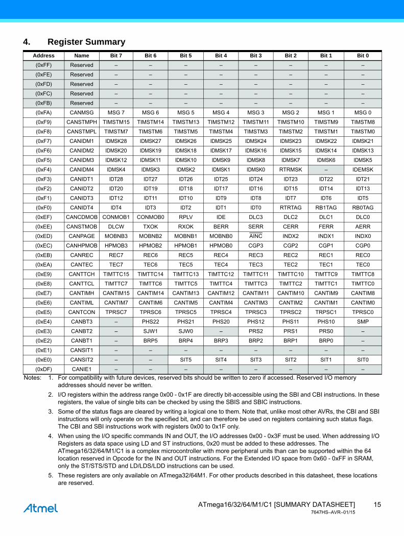
4. Register Summary
Address Name Bit 7 Bit 6 Bit 5 Bit 4 Bit 3 Bit 2 Bit 1 Bit 0
(0xFF) Reserved – – – – – – – –
(0xFE) Reserved – – – – – – – –
(0xFD) Reserved – – – – – – – –
(0xFC) Reserved – – – – – – – –
(0xFB) Reserved – – – – – – – –
(0xFA) CANMSG MSG 7 MSG 6 MSG 5 MSG 4 MSG 3 MSG 2 MSG 1 MSG 0
(0xF9) CANSTMPH TIMSTM15 TIMSTM14 TIMSTM13 TIMSTM12 TIMSTM11 TIMSTM10 TIMSTM9 TIMSTM8
(0xF8) CANSTMPL TIMSTM7 TIMSTM6 TIMSTM5 TIMSTM4 TIMSTM3 TIMSTM2 TIMSTM1 TIMSTM0
(0xF7) CANIDM1 IDMSK28 IDMSK27 IDMSK26 IDMSK25 IDMSK24 IDMSK23 IDMSK22 IDMSK21
(0xF6) CANIDM2 IDMSK20 IDMSK19 IDMSK18 IDMSK17 IDMSK16 IDMSK15 IDMSK14 IDMSK13
(0xF5) CANIDM3 IDMSK12 IDMSK11 IDMSK10 IDMSK9 IDMSK8 IDMSK7 IDMSK6 IDMSK5
(0xF4) CANIDM4 IDMSK4 IDMSK3 IDMSK2 IDMSK1 IDMSK0 RTRMSK – IDEMSK
(0xF3) CANIDT1 IDT28 IDT27 IDT26 IDT25 IDT24 IDT23 IDT22 IDT21
(0xF2) CANIDT2 IDT20 IDT19 IDT18 IDT17 IDT16 IDT15 IDT14 IDT13
(0xF1) CANIDT3 IDT12 IDT11 IDT10 IDT9 IDT8 IDT7 IDT6 IDT5
(0xF0) CANIDT4 IDT4 IDT3 IDT2 IDT1 IDT0 RTRTAG RB1TAG RB0TAG
(0xEF) CANCDMOB CONMOB1 CONMOB0 RPLV IDE DLC3 DLC2 DLC1 DLC0
(0xEE) CANSTMOB DLCW TXOK RXOK BERR SERR CERR FERR AERR
(0xED) CANPAGE MOBNB3 MOBNB2 MOBNB1 MOBNB0 AINC INDX2 INDX1 INDX0
(0xEC) CANHPMOB HPMOB3 HPMOB2 HPMOB1 HPMOB0 CGP3 CGP2 CGP1 CGP0
(0xEB) CANREC REC7 REC6 REC5 REC4 REC3 REC2 REC1 REC0
(0xEA) CANTEC TEC7 TEC6 TEC5 TEC4 TEC3 TEC2 TEC1 TEC0
(0xE9) CANTTCH TIMTTC15 TIMTTC14 TIMTTC13 TIMTTC12 TIMTTC11 TIMTTC10 TIMTTC9 TIMTTC8
(0xE8) CANTTCL TIMTTC7 TIMTTC6 TIMTTC5 TIMTTC4 TIMTTC3 TIMTTC2 TIMTTC1 TIMTTC0
(0xE7) CANTIMH CANTIM15 CANTIM14 CANTIM13 CANTIM12 CANTIM11 CANTIM10 CANTIM9 CANTIM8
(0xE6) CANTIML CANTIM7 CANTIM6 CANTIM5 CANTIM4 CANTIM3 CANTIM2 CANTIM1 CANTIM0
(0xE5) CANTCON TPRSC7 TPRSC6 TPRSC5 TPRSC4 TPRSC3 TPRSC2 TRPSC1 TPRSC0
(0xE4) CANBT3 – PHS22 PHS21 PHS20 PHS12 PHS11 PHS10 SMP
(0xE3) CANBT2 – SJW1 SJW0 – PRS2 PRS1 PRS0 –
(0xE2) CANBT1 – BRP5 BRP4 BRP3 BRP2 BRP1 BRP0 –
(0xE1) CANSIT1 – – – – – – – –
(0xE0) CANSIT2 – – SIT5 SIT4 SIT3 SIT2 SIT1 SIT0
(0xDF) CANIE1 – – – – – – – –
Notes: 1. For compatibility with future devices, reserved bits should be written to zero if accessed. Reserved I/O memory addresses should never be written.
2. I/O registers within the address range 0x00 - 0x1F are directly bit-accessible using the SBI and CBI instructions. In these registers, the value of single bits can be checked by using the SBIS and SBIC instructions.
3. Some of the status flags are cleared by writing a logical one to them. Note that, unlike most other AVRs, the CBI and SBI instructions will only operate on the specified bit, and can therefore be used on registers containing such status flags. The CBI and SBI instructions work with registers 0x00 to 0x1F only.
4. When using the I/O specific commands IN and OUT, the I/O addresses 0x00 - 0x3F must be used. When addressing I/O Registers as data space using LD and ST instructions, 0x20 must be added to these addresses. The ATmega16/32/64/M1/C1 is a complex microcontroller with more peripheral units than can be supported within the 64 location reserved in Opcode for the IN and OUT instructions. For the Extended I/O space from 0x60 - 0xFF in SRAM, only the ST/STS/STD and LD/LDS/LDD instructions can be used.
5. These registers are only available on ATmega32/64M1. For other products described in this datasheet, these locations are reserved.
15ATmega16/32/64/M1/C1 [SUMMARY DATASHEET]7647HS–AVR–01/15

(0xDE) CANIE2 – – IEMOB5 IEMOB4 IEMOB3 IEMOB2 IEMOB1 IEMOB0
(0xDD) CANEN1 – – – – – – – –
(0xDC) CANEN2 – – ENMOB5 ENMOB4 ENMOB3 ENMOB2 ENMOB1 ENMOB0
(0xDB) CANGIE ENIT ENBOFF ENRX ENTX ENERR ENBX ENERG ENOVRT
(0xDA) CANGIT CANIT BOFFIT OVRTIM BXOK SERG CERG FERG AERG
(0xD9) CANGSTA – OVRG – TXBSY RXBSY ENFG BOFF ERRP
(0xD8) CANGCON ABRQ OVRQ TTC SYNTTC LISTEN TEST ENA/STB SWRES
(0xD7) Reserved – – – – – – – –
(0xD6) Reserved – – – – – – – –
(0xD5) Reserved – – – – – – – –
(0xD4) Reserved – – – – – – – –
(0xD3) Reserved – – – – – – – –
(0xD2) LINDAT LDATA7 LDATA6 LDATA5 LDATA4 LDATA3 LDATA2 LDATA1 LDATA0
(0xD1) LINSEL – – – – /LAINC LINDX2 LINDX1 LINDX0
(0xD0) LINIDR LP1 LP0 LID5 / LDL1 LID4 / LDL0 LID3 LID2 LID1 LID0
(0xCF) LINDLR LTXDL3 LTXDL2 LTXDL1 LTXDL0 LRXDL3 LRXDL2 LRXDL1 LRXDL0
(0xCE) LINBRRH – – – – LDIV11 LDIV10 LDIV9 LDIV8
(0xCD) LINBRRL LDIV7 LDIV6 LDIV5 LDIV4 LDIV3 LDIV2 LDIV1 LDIV0
(0xCC) LINBTR LDISR – LBT5 LBT4 LBT3 LBT2 LBT1 LBT0
(0xCB) LINERR LABORT LTOERR LOVERR LFERR LSERR LPERR LCERR LBERR
(0xCA) LINENIR – – – – LENERR LENIDOK LENTXOK LENRXOK
(0xC9) LINSIR LIDST2 LIDST1 LIDST0 LBUSY LERR LIDOK LTXOK LRXOK
(0xC8) LINCR LSWRES LIN13 LCONF1 LCONF0 LENA LCMD2 LCMD1 LCMD0
(0xC7) Reserved – – – – – – – –
(0xC6) Reserved – – – – – – – –
(0xC5) Reserved – – – – – – – –
(0xC4) Reserved – – – – – – – –
(0xC3) Reserved – – – – – – – –
(0xC2) Reserved – – – – – – – –
(0xC1) Reserved – – – – – – – –
(0xC0) Reserved – – – – – – – –
(0xBF) Reserved – – – – – – – –
(0xBE) Reserved – – – – – – – –
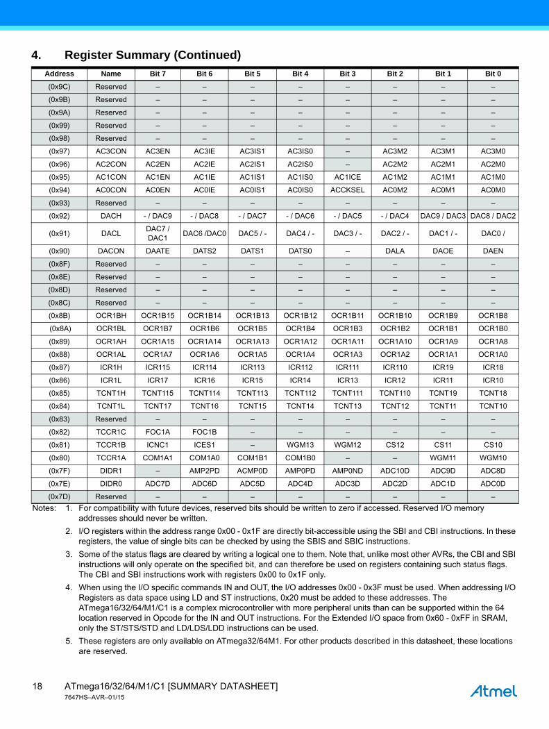
4. Register Summary (Continued)
Address Name Bit 7 Bit 6 Bit 5 Bit 4 Bit 3 Bit 2 Bit 1 Bit 0
Notes: 1. For compatibility with future devices, reserved bits should be written to zero if accessed. Reserved I/O memory addresses should never be written.
2. I/O registers within the address range 0x00 - 0x1F are directly bit-accessible using the SBI and CBI instructions. In these registers, the value of single bits can be checked by using the SBIS and SBIC instructions.
3. Some of the status flags are cleared by writing a logical one to them. Note that, unlike most other AVRs, the CBI and SBI instructions will only operate on the specified bit, and can therefore be used on registers containing such status flags. The CBI and SBI instructions work with registers 0x00 to 0x1F only.
4. When using the I/O specific commands IN and OUT, the I/O addresses 0x00 - 0x3F must be used. When addressing I/O Registers as data space using LD and ST instructions, 0x20 must be added to these addresses. The ATmega16/32/64/M1/C1 is a complex microcontroller with more peripheral units than can be supported within the 64 location reserved in Opcode for the IN and OUT instructions. For the Extended I/O space from 0x60 - 0xFF in SRAM, only the ST/STS/STD and LD/LDS/LDD instructions can be used.
5. These registers are only available on ATmega32/64M1. For other products described in this datasheet, these locations are reserved.
ATmega16/32/64/M1/C1 [SUMMARY DATASHEET]7647HS–AVR–01/15
16

(0xBD) Reserved – – – – – – – –
(0xBC)(5) PIFR – – – – PEV2 PEV1 PEV0 PEOP
(0xBB)(5) PIM – – – – PEVE2 PEVE1 PEVE0 PEOPE
(0xBA)(5) PMIC2 POVEN2 PISEL2 PELEV2 PFLTE2 PAOC2 PRFM22 PRFM21 PRFM20
(0xB9)(5) PMIC1 POVEN1 PISEL1 PELEV1 PFLTE1 PAOC1 PRFM12 PRFM11 PRFM10
(0xB8)(5) PMIC0 POVEN0 PISEL0 PELEV0 PFLTE0 PAOC0 PRFM02 PRFM01 PRFM00
(0xB7)(5) PCTL PPRE1 PPRE0 PCLKSEL – – – PCCYC PRUN
(0xB6)(5) POC – – POEN2B POEN2A POEN1B POEN1A POEN0B POEN0A
(0xB5)(5) PCNF – – PULOCK PMODE POPB POPA – –
(0xB4)(5) PSYNC – – PSYNC21 PSYNC20 PSYNC11 PSYNC10 PSYNC01 PSYNC00
(0xB3)(5) POCR_RBH – – – – POCR_RB11 POCR_RB10 POCR_RB9 POCR_RB8
(0xB2)(5) POCR_RBL POCR_RB7 POCR_RB6 POCR_RB5 POCR_RB4 POCR_RB3 POCR_RB2 POCR_RB1 POCR_RB0
(0xB1)(5) POCR2SBH – – – – POCR2SB11 POCR2SB10 POCR2SB9 POCR2SB8
(0xB0)(5) POCR2SBL POCR2SB7 POCR2SB6 POCR2SB5 POCR2SB4 POCR2SB3 POCR2SB2 POCR2SB1 POCR2SB0
(0xAF)(5) POCR2RAH – – – – POCR2RA11 POCR2RA10 POCR2RA9 POCR2RA8
(0xAE)(5) POCR2RAL POCR2RA7 POCR2RA6 POCR2RA5 POCR2RA4 POCR2RA3 POCR2RA2 POCR2RA1 POCR2RA0
(0xAD)(5) POCR2SAH – – – – POCR2SA11 POCR2SA10 POCR2SA9 POCR2SA8
(0xAC)(5) POCR2SAL POCR2SA7 POCR2SA6 POCR2SA5 POCR2SA4 POCR2SA3 POCR2SA2 POCR2SA1 POCR2SA0
(0xAB)(5) POCR1SBH – – – – POCR1SB11 POCR1SB10 POCR1SB9 POCR1SB8
(0xAA)(5) POCR1SBL POCR1SB7 POCR1SB6 POCR1SB5 POCR1SB4 POCR1SB3 POCR1SB2 POCR1SB1 POCR1SB0
(0xA9)(5) POCR1RAH – – – – POCR1RA11 POCR1RA10 POCR1RA9 POCR1RA8
(0xA8)(5) POCR1RAL POCR1RA7 POCR1RA6 POCR1RA5 POCR1RA4 POCR1RA3 POCR1RA2 POCR1RA1 POCR1RA0
(0xA7)(5) POCR1SAH – – – – POCR1SA11 POCR1SA10 POCR1SA9 POCR1SA8
(0xA6)(5) POCR1SAL POCR1SA7 POCR1SA6 POCR1SA5 POCR1SA4 POCR1SA3 POCR1SA2 POCR1SA1 POCR1SA0
(0xA5)(5) POCR0SBH – – – – POCR0SB11 POCR0SB10 POCR0SB9 POCR0SB8
(0xA4)(5) POCR0SBL POCR0SB7 POCR0SB6 POCR0SB5 POCR0SB4 POCR0SB3 POCR0SB2 POCR0SB1 POCR0SB0
(0xA3)(5) POCR0RAH – – – – POCR0RA11 POCR0RA10 POCR0RA9 POCR0RA8
(0xA2)(5) POCR0RAL POCR0RA7 POCR0RA6 POCR0RA5 POCR0RA4 POCR0RA3 POCR0RA2 POCR0RA1 POCR0RA0
(0xA1)(5) POCR0SAH – – – – POCR0SA11 POCR0SA10 POCR0SA9 POCR0SA8
(0xA0)(5) POCR0SAL POCR0SA7 POCR0SA6 POCR0SA5 POCR0SA4 POCR0SA3 POCR0SA2 POCR0SA1 POCR0SA0
(0x9F) Reserved – – – – – – – –
(0x9E) Reserved – – – – – – – –
(0x9D) Reserved – – – – – – – –
4. Register Summary (Continued)
Address Name Bit 7 Bit 6 Bit 5 Bit 4 Bit 3 Bit 2 Bit 1 Bit 0
Notes: 1. For compatibility with future devices, reserved bits should be written to zero if accessed. Reserved I/O memory addresses should never be written.
2. I/O registers within the address range 0x00 - 0x1F are directly bit-accessible using the SBI and CBI instructions. In these registers, the value of single bits can be checked by using the SBIS and SBIC instructions.
3. Some of the status flags are cleared by writing a logical one to them. Note that, unlike most other AVRs, the CBI and SBI instructions will only operate on the specified bit, and can therefore be used on registers containing such status flags. The CBI and SBI instructions work with registers 0x00 to 0x1F only.
4. When using the I/O specific commands IN and OUT, the I/O addresses 0x00 - 0x3F must be used. When addressing I/O Registers as data space using LD and ST instructions, 0x20 must be added to these addresses. The ATmega16/32/64/M1/C1 is a complex microcontroller with more peripheral units than can be supported within the 64 location reserved in Opcode for the IN and OUT instructions. For the Extended I/O space from 0x60 - 0xFF in SRAM, only the ST/STS/STD and LD/LDS/LDD instructions can be used.
5. These registers are only available on ATmega32/64M1. For other products described in this datasheet, these locations are reserved.
17ATmega16/32/64/M1/C1 [SUMMARY DATASHEET]7647HS–AVR–01/15
(0x9C) Reserved – – – – – – – –
(0x9B) Reserved – – – – – – – –
(0x9A) Reserved – – – – – – – –
(0x99) Reserved – – – – – – – –
(0x98) Reserved – – – – – – – –
(0x97) AC3CON AC3EN AC3IE AC3IS1 AC3IS0 – AC3M2 AC3M1 AC3M0
(0x96) AC2CON AC2EN AC2IE AC2IS1 AC2IS0 – AC2M2 AC2M1 AC2M0
(0x95) AC1CON AC1EN AC1IE AC1IS1 AC1IS0 AC1ICE AC1M2 AC1M1 AC1M0
(0x94) AC0CON AC0EN AC0IE AC0IS1 AC0IS0 ACCKSEL AC0M2 AC0M1 AC0M0
(0x93) Reserved – – – – – – – –
(0x92) DACH - / DAC9 - / DAC8 - / DAC7 - / DAC6 - / DAC5 - / DAC4 DAC9 / DAC3 DAC8 / DAC2
(0x91) DACLDAC7 / DAC1
DAC6 /DAC0 DAC5 / - DAC4 / - DAC3 / - DAC2 / - DAC1 / - DAC0 /
(0x90) DACON DAATE DATS2 DATS1 DATS0 – DALA DAOE DAEN
(0x8F) Reserved – – – – – – – –
(0x8E) Reserved – – – – – – – –
(0x8D) Reserved – – – – – – – –
(0x8C) Reserved – – – – – – – –
(0x8B) OCR1BH OCR1B15 OCR1B14 OCR1B13 OCR1B12 OCR1B11 OCR1B10 OCR1B9 OCR1B8
(0x8A) OCR1BL OCR1B7 OCR1B6 OCR1B5 OCR1B4 OCR1B3 OCR1B2 OCR1B1 OCR1B0
(0x89) OCR1AH OCR1A15 OCR1A14 OCR1A13 OCR1A12 OCR1A11 OCR1A10 OCR1A9 OCR1A8
(0x88) OCR1AL OCR1A7 OCR1A6 OCR1A5 OCR1A4 OCR1A3 OCR1A2 OCR1A1 OCR1A0
(0x87) ICR1H ICR115 ICR114 ICR113 ICR112 ICR111 ICR110 ICR19 ICR18
(0x86) ICR1L ICR17 ICR16 ICR15 ICR14 ICR13 ICR12 ICR11 ICR10
(0x85) TCNT1H TCNT115 TCNT114 TCNT113 TCNT112 TCNT111 TCNT110 TCNT19 TCNT18
(0x84) TCNT1L TCNT17 TCNT16 TCNT15 TCNT14 TCNT13 TCNT12 TCNT11 TCNT10
(0x83) Reserved – – – – – – – –
(0x82) TCCR1C FOC1A FOC1B – – – – – –
(0x81) TCCR1B ICNC1 ICES1 – WGM13 WGM12 CS12 CS11 CS10
(0x80) TCCR1A COM1A1 COM1A0 COM1B1 COM1B0 – – WGM11 WGM10
(0x7F) DIDR1 – AMP2PD ACMP0D AMP0PD AMP0ND ADC10D ADC9D ADC8D
(0x7E) DIDR0 ADC7D ADC6D ADC5D ADC4D ADC3D ADC2D ADC1D ADC0D
(0x7D) Reserved – – – – – – – –
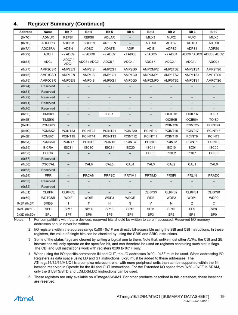
4. Register Summary (Continued)
Address Name Bit 7 Bit 6 Bit 5 Bit 4 Bit 3 Bit 2 Bit 1 Bit 0
Notes: 1. For compatibility with future devices, reserved bits should be written to zero if accessed. Reserved I/O memory addresses should never be written.
2. I/O registers within the address range 0x00 - 0x1F are directly bit-accessible using the SBI and CBI instructions. In these registers, the value of single bits can be checked by using the SBIS and SBIC instructions.
3. Some of the status flags are cleared by writing a logical one to them. Note that, unlike most other AVRs, the CBI and SBI instructions will only operate on the specified bit, and can therefore be used on registers containing such status flags. The CBI and SBI instructions work with registers 0x00 to 0x1F only.
4. When using the I/O specific commands IN and OUT, the I/O addresses 0x00 - 0x3F must be used. When addressing I/O Registers as data space using LD and ST instructions, 0x20 must be added to these addresses. The ATmega16/32/64/M1/C1 is a complex microcontroller with more peripheral units than can be supported within the 64 location reserved in Opcode for the IN and OUT instructions. For the Extended I/O space from 0x60 - 0xFF in SRAM, only the ST/STS/STD and LD/LDS/LDD instructions can be used.
5. These registers are only available on ATmega32/64M1. For other products described in this datasheet, these locations are reserved.
ATmega16/32/64/M1/C1 [SUMMARY DATASHEET]7647HS–AVR–01/15
18
(0x7C) ADMUX REFS1 REFS0 ADLAR – MUX3 MUX2 MUX1 MUX0
(0x7B) ADCSRB ADHSM ISRCEN AREFEN – ADTS3 ADTS2 ADTS1 ADTS0
(0x7A) ADCSRA ADEN ADSC ADATE ADIF ADIE ADPS2 ADPS1 ADPS0
(0x79) ADCH - / ADC9 - / ADC8 - / ADC7 - / ADC6 - / ADC5 - / ADC4 ADC9 / ADC3 ADC8 / ADC2
(0x78) ADCLADC7 / ADC1
ADC6 / ADC0 ADC5 / - ADC4 / - ADC3 / - ADC2 / - ADC1 / - ADC0 /
(0x77) AMP2CSR AMP2EN AMP2IS AMP2G1 AMP2G0 AMPCMP2 AMP2TS2 AMP2TS1 AMP2TS0
(0x76) AMP1CSR AMP1EN AMP1IS AMP1G1 AMP1G0 AMPCMP1 AMP1TS2 AMP1TS1 AMP1TS0
(0x75) AMP0CSR AMP0EN AMP0IS AMP0G1 AMP0G0 AMPCMP0 AMP0TS2 AMP0TS1 AMP0TS0
(0x74) Reserved – – – – – – – –
(0x73) Reserved – – – – – – – –
(0x72) Reserved – – – – – – – –
(0x71) Reserved – – – – – – – –
(0x70) Reserved – – – – – – – –
(0x6F) TIMSK1 – – ICIE1 – – OCIE1B OCIE1A TOIE1
(0x6E) TIMSK0 – – – – – OCIE0B OCIE0A TOIE0
(0x6D) PCMSK3 – – – – – PCINT26 PCINT25 PCINT24
(0x6C) PCMSK2 PCINT23 PCINT22 PCINT21 PCINT20 PCINT19 PCINT18 PCINT17 PCINT16
(0x6B) PCMSK1 PCINT15 PCINT14 PCINT13 PCINT12 PCINT11 PCINT10 PCINT9 PCINT8
(0x6A) PCMSK0 PCINT7 PCINT6 PCINT5 PCINT4 PCINT3 PCINT2 PCINT1 PCINT0
(0x69) EICRA ISC31 ISC30 ISC21 ISC20 ISC11 ISC10 ISC01 ISC00
(0x68) PCICR – – – – PCIE3 PCIE2 PCIE1 PCIE0
(0x67) Reserved – – – – – – – –
(0x66) OSCCAL – CAL6 CAL5 CAL4 CAL3 CAL2 CAL1 CAL0
(0x65) Reserved – – – – – – – –
(0x64) PRR – PRCAN PRPSC PRTIM1 PRTIM0 PRSPI PRLIN PRADC
(0x63) Reserved – – – – – – – –
(0x62) Reserved – – – – – – – –
(0x61) CLKPR CLKPCE – – – CLKPS3 CLKPS2 CLKPS1 CLKPS0
(0x60) WDTCSR WDIF WDIE WDP3 WDCE WDE WDP2 WDP1 WDP0
0x3F (0x5F) SREG I T H S V N Z C
0x3E (0x5E) SPH SP15 SP14 SP13 SP12 SP11 SP10 SP9 SP8
0x3D (0x5D) SPL SP7 SP6 SP5 SP4 SP3 SP2 SP1 SP0
4. Register Summary (Continued)
Address Name Bit 7 Bit 6 Bit 5 Bit 4 Bit 3 Bit 2 Bit 1 Bit 0
Notes: 1. For compatibility with future devices, reserved bits should be written to zero if accessed. Reserved I/O memory addresses should never be written.
2. I/O registers within the address range 0x00 - 0x1F are directly bit-accessible using the SBI and CBI instructions. In these registers, the value of single bits can be checked by using the SBIS and SBIC instructions.
3. Some of the status flags are cleared by writing a logical one to them. Note that, unlike most other AVRs, the CBI and SBI instructions will only operate on the specified bit, and can therefore be used on registers containing such status flags. The CBI and SBI instructions work with registers 0x00 to 0x1F only.
4. When using the I/O specific commands IN and OUT, the I/O addresses 0x00 - 0x3F must be used. When addressing I/O Registers as data space using LD and ST instructions, 0x20 must be added to these addresses. The ATmega16/32/64/M1/C1 is a complex microcontroller with more peripheral units than can be supported within the 64 location reserved in Opcode for the IN and OUT instructions. For the Extended I/O space from 0x60 - 0xFF in SRAM, only the ST/STS/STD and LD/LDS/LDD instructions can be used.
5. These registers are only available on ATmega32/64M1. For other products described in this datasheet, these locations are reserved.
19ATmega16/32/64/M1/C1 [SUMMARY DATASHEET]7647HS–AVR–01/15
0x3C (0x5C) Reserved – – – – – – – –
0x3B (0x5B) Reserved – – – – – – – –
0x3A (0x5A) Reserved – – – – – – – –
0x39 (0x59) Reserved – – – – – – – –
0x38 (0x58) Reserved – – – – – – – –
0x37 (0x57) SPMCSR SPMIE RWWSB SIGRD RWWSRE BLBSET PGWRT PGERS SPMEN
0x36 (0x56) Reserved – – – – – – – –
0x35 (0x55) MCUCR SPIPS – – PUD – – IVSEL IVCE
0x34 (0x54) MCUSR – – – – WDRF BORF EXTRF PORF
0x33 (0x53) SMCR – – – – SM2 SM1 SM0 SE
0x32 (0x52) MSMCR Monitor Stop Mode Control Register
0x31 (0x51) MONDR Monitor Data Register
0x30 (0x50) ACSR AC3IF AC2IF AC1IF AC0IF AC3O AC2O AC1O AC0O
0x2F (0x4F) Reserved – – – – – – – –
0x2E (0x4E) SPDR SPD7 SPD6 SPD5 SPD4 SPD3 SPD2 SPD1 SPD0
0x2D (0x4D) SPSR SPIF WCOL – – – – – SPI2X
0x2C (0x4C) SPCR SPIE SPE DORD MSTR CPOL CPHA SPR1 SPR0
0x2B (0x4B) Reserved – – – – – – – –
0x2A (0x4A) Reserved – – – – – – – –
0x29 (0x49) PLLCSR – – – – – PLLF PLLE PLOCK
0x28 (0x48) OCR0B OCR0B7 OCR0B6 OCR0B5 OCR0B4 OCR0B3 OCR0B2 OCR0B1 OCR0B0
0x27 (0x47) OCR0A OCR0A7 OCR0A6 OCR0A5 OCR0A4 OCR0A3 OCR0A2 OCR0A1 OCR0A0
0x26 (0x46) TCNT0 TCNT07 TCNT06 TCNT05 TCNT04 TCNT03 TCNT02 TCNT01 TCNT00
0x25 (0x45) TCCR0B FOC0A FOC0B – – WGM02 CS02 CS01 CS00
0x24 (0x44) TCCR0A COM0A1 COM0A0 COM0B1 COM0B0 – – WGM01 WGM00
0x23 (0x43) GTCCR TSM ICPSEL1 – – – – – PSRSYNC
0x22 (0x42) EEARH – – – – – – EEAR9 EEAR8
0x21 (0x41) EEARL EEAR7 EEAR6 EEAR5 EEAR4 EEAR3 EEAR2 EEAR1 EEAR0
0x20 (0x40) EEDR EEDR7 EEDR6 EEDR5 EEDR4 EEDR3 EEDR2 EEDR1 EEDR0
0x1F (0x3F) EECR – – – – EERIE EEMWE EEWE EERE
0x1E (0x3E) GPIOR0 GPIOR07 GPIOR06 GPIOR05 GPIOR04 GPIOR03 GPIOR02 GPIOR01 GPIOR00
0x1D (0x3D) EIMSK – – – – INT3 INT2 INT1 INT0
0x1C (0x3C) EIFR – – – – INTF3 INTF2 INTF1 INTF0
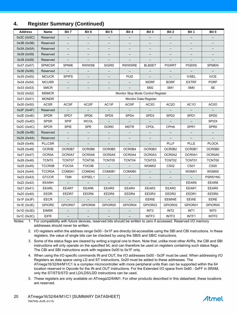
4. Register Summary (Continued)
Address Name Bit 7 Bit 6 Bit 5 Bit 4 Bit 3 Bit 2 Bit 1 Bit 0
Notes: 1. For compatibility with future devices, reserved bits should be written to zero if accessed. Reserved I/O memory addresses should never be written.
2. I/O registers within the address range 0x00 - 0x1F are directly bit-accessible using the SBI and CBI instructions. In these registers, the value of single bits can be checked by using the SBIS and SBIC instructions.
3. Some of the status flags are cleared by writing a logical one to them. Note that, unlike most other AVRs, the CBI and SBI instructions will only operate on the specified bit, and can therefore be used on registers containing such status flags. The CBI and SBI instructions work with registers 0x00 to 0x1F only.
4. When using the I/O specific commands IN and OUT, the I/O addresses 0x00 - 0x3F must be used. When addressing I/O Registers as data space using LD and ST instructions, 0x20 must be added to these addresses. The ATmega16/32/64/M1/C1 is a complex microcontroller with more peripheral units than can be supported within the 64 location reserved in Opcode for the IN and OUT instructions. For the Extended I/O space from 0x60 - 0xFF in SRAM, only the ST/STS/STD and LD/LDS/LDD instructions can be used.
5. These registers are only available on ATmega32/64M1. For other products described in this datasheet, these locations are reserved.
ATmega16/32/64/M1/C1 [SUMMARY DATASHEET]7647HS–AVR–01/15
20

0x1B (0x3B) PCIFR – – – – PCIF3 PCIF2 PCIF1 PCIF0
0x1A (0x3A) GPIOR2 GPIOR27 GPIOR26 GPIOR25 GPIOR24 GPIOR23 GPIOR22 GPIOR21 GPIOR20
0x19 (0x39) GPIOR1 GPIOR17 GPIOR16 GPIOR15 GPIOR14 GPIOR13 GPIOR12 GPIOR11 GPIOR10
0x18 (0x38) Reserved – – – – – – – –
0x17 (0x37) Reserved – – – – – – – –
0x16 (0x36) TIFR1 – – ICF1 – – OCF1B OCF1A TOV1
0x15 (0x35) TIFR0 – – – – – OCF0B OCF0A TOV0
0x14 (0x34) Reserved – – – – – – – –
0x13 (0x33) Reserved – – – – – – – –
0x12 (0x32) Reserved – – – – – – – –
0x11 (0x31) Reserved – – – – – – – –
0x10 (0x30) Reserved – – – – – – – –
0x0F (0x2F) Reserved – – – – – – – –
0x0E (0x2E) PORTE – – – – – PORTE2 PORTE1 PORTE0
0x0D (0x2D) DDRE – – – – – DDE2 DDE1 DDE0
0x0C (0x2C) PINE – – – – – PINE2 PINE1 PINE0
0x0B (0x2B) PORTD PORTD7 PORTD6 PORTD5 PORTD4 PORTD3 PORTD2 PORTD1 PORTD0
0x0A (0x2A) DDRD DDD7 DDD6 DDD5 DDD4 DDD3 DDD2 DDD1 DDD0
0x09 (0x29) PIND PIND7 PIND6 PIND5 PIND4 PIND3 PIND2 PIND1 PIND0
0x08 (0x28) PORTC PORTC7 PORTC6 PORTC5 PORTC4 PORTC3 PORTC2 PORTC1 PORTC0
0x07 (0x27) DDRC DDC7 DDC6 DDC5 DDC4 DDC3 DDC2 DDC1 DDC0
0x06 (0x26) PINC PINC7 PINC6 PINC5 PINC4 PINC3 PINC2 PINC1 PINC0
0x05 (0x25) PORTB PORTB7 PORTB6 PORTB5 PORTB4 PORTB3 PORTB2 PORTB1 PORTB0
0x04 (0x24) DDRB DDB7 DDB6 DDB5 DDB4 DDB3 DDB2 DDB1 DDB0
0x03 (0x23) PINB PINB7 PINB6 PINB5 PINB4 PINB3 PINB2 PINB1 PINB0
0x02 (0x22) Reserved – – – – – – – –
0x01 (0x21) Reserved – – – – – – – –
0x00 (0x20) Reserved – – – – – – – –
4. Register Summary (Continued)
Address Name Bit 7 Bit 6 Bit 5 Bit 4 Bit 3 Bit 2 Bit 1 Bit 0
Notes: 1. For compatibility with future devices, reserved bits should be written to zero if accessed. Reserved I/O memory addresses should never be written.
2. I/O registers within the address range 0x00 - 0x1F are directly bit-accessible using the SBI and CBI instructions. In these registers, the value of single bits can be checked by using the SBIS and SBIC instructions.
3. Some of the status flags are cleared by writing a logical one to them. Note that, unlike most other AVRs, the CBI and SBI instructions will only operate on the specified bit, and can therefore be used on registers containing such status flags. The CBI and SBI instructions work with registers 0x00 to 0x1F only.
4. When using the I/O specific commands IN and OUT, the I/O addresses 0x00 - 0x3F must be used. When addressing I/O Registers as data space using LD and ST instructions, 0x20 must be added to these addresses. The ATmega16/32/64/M1/C1 is a complex microcontroller with more peripheral units than can be supported within the 64 location reserved in Opcode for the IN and OUT instructions. For the Extended I/O space from 0x60 - 0xFF in SRAM, only the ST/STS/STD and LD/LDS/LDD instructions can be used.
5. These registers are only available on ATmega32/64M1. For other products described in this datasheet, these locations are reserved.
21ATmega16/32/64/M1/C1 [SUMMARY DATASHEET]7647HS–AVR–01/15
5. Errata
5.1 Errata Summary
5.1.1 ATmega16M1/16C1/32M1/32C1 Rev. C (Mask Revision)
● LIN break delimiter
● ADC with PSC2-synchronized
● ADC amplifier measurement is unstable
5.1.2 ATmega16M1/16C1/32M1/32C1 Rev. B (Mask Revision)
● The AMPCMPx bits return 0
● No comparison when amplifier is used as comparator input and ADC input
● CRC calculation of diagnostic frames in LIN 2.x.
● Wrong TSOFFSET manufacturing calibration value
● PD0-PD3 set to outputs and PD4 pulled down following power-on with external reset active.
● LIN Break Delimiter
● ADC with PSC2-synchronized
● ADC amplifier measurement is unstable
● PSC emulation
● PSC OCRxx register update according to PLOCK2 usage
● Read/write instructions of MUXn and REFS1:0
5.1.3 ATmega16M1/16C1/32M1/32C1 Rev. A (Mask Revision)
● Inopportune reset of the CANIDM registers
● The AMPCMPx bits return 0
● No comparison when amplifier is used as comparator input and ADC input
● CRC calculation of diagnostic frames in LIN 2.x
● PD0-PD3 set to outputs and PD4 pulled down following power-on with external reset active
● LIN break delimiter
● ADC with PSC2-synchronized
● ADC amplifier measurement is unstable
● PSC emulation
● Read/write instructions of MUXn and REFS1:0
5.1.4 Errata Description
1. Inopportune Reset of the CANIDM RegistersAfter the reception of a CAN frame in a MOb, the ID mask registers are reset.Problem Fix / WorkaroundBefore enabling a MOb in reception, re-initialize the ID mask registers - CANIDM[4..1].
2. The AMPCMPx Bits Return 0When they are read the AMPCMPx bits in AMPxCSR registers return 0.Problem Fix / WorkaroundIf the reading of the AMPCMPx bits is required, store the AMPCMPx value in a variable in memory before writing in the AMPxCSR register and read the variable when necessary.
3. No Comparison when Amplifier is used as Comparator Input and ADC InputWhen it is selected as ADC input, an amplifier receives no clock signal when the ADC is stopped. In that case, if the amplifier is also used as comparator input, no analog signal is propagated and no comparison is done.Problem Fix / WorkaroundSelect another ADC channel rather than the working amplified channel.
ATmega16/32/64/M1/C1 [SUMMARY DATASHEET]7647HS–AVR–01/15
22
4. CRC Calculation of Diagnostic Frames in LIN 2.x.Diagnostic frames of LIN 2.x use “classic checksum” calculation. Unfortunately, the setting of the checksum model is enabled when the HEADER is transmitted/received. Usually, in LIN 2.x the LIN/UART controller is initialized to process “enhanced checksums” and a slave task does not know what kind of frame it will work on before checking the ID.Problem Fix / WorkaroundThis workaround is to be implemented only in case of transmission/reception of diagnostics frames.
a. Slave task of master node:Before enabling the HEADER, the master must set the appropriate LIN13 bitvalue in LINCR register.
b. For slaves nodes, the workaround is in 2 parts:
– Before enabling the RESPONSE, use the following function:
void lin_wa_head(void) {unsigned char temp; temp = LINBTR;LINCR = 0x00; // It is not a RESET !LINBTR = (1<<LDISR)|temp;LINCR = (1<<LIN13)|(1<<LENA)|(0<<LCMD2)|(0<<LCMD1)|(0<<LCMD0);LINDLR = 0x88; // If it isn't already done}– Once the RESPONSE is received or sent (having RxOK or TxOK as well as LERR), use the following function:void lin_wa_tail(void) {LINCR = 0x00; // It is not a RESET !LINBTR = 0x00;LINCR = (0<<LIN13)|(1<<LENA)|(0<<LCMD2)|(0<<LCMD1)|(0<<LCMD0);}
The time-out counter is disabled during the RESPONSE when the workaround is set.
5. Wrong TSOFFSET Manufacturing Calibration value.Erroneous value of TSOFFSET programmed in signature byte.(TSOFFSET was introduced from REVB silicon).Problem Fix / WorkaroundTo identify RevB with wrong TSOFFSET value, check device signature byte at address 0X3F if value is not 0X42 (Ascii code ‘B’) then use the following formula.TS_OFFSET(True) = (150*(1-TS_GAIN))+TS_OFFSET.
6. PD0-PD3 Set to Outputs and PD4 Pulled Down following Power-on with Eternal Reset Active.At power-on with the external reset signal active the four I/O lines PD0-PD3 may be forced into an output state. Normally these lines should be in an input state. PD4 may be pulled down with internal 220k resistor. Following release of the reset line (whatever is the startup time) with the clock running the I/Os PD0-PD4 will adopt their intended input state.Problem Fix / WorkaroundNone
7. LIN Break DelimitterIn SLAVE MODE, a BREAK field detection error can occur under following conditions. The problem occurs if 2 conditions occur simultaneously:
a. The DOMINANT part of the BREAK is (N+0.5)*Tbit long with N=13, 14,15,
b. The RECESSIVE part of the BREAK (BREAK DELIMITER) is equal to 1*Tbit. (see note below)
The BREAK_high is not detected, and the 2nd bit of the SYNC field is interpreted as the BREAK DELIMITER. The error is detected as a framing error on the first bits of the PID or on subsequent Data or a Checksum error. There is no error if BREAK_high is greater than 1 Tbit + 18%. There is no problem in Master mode.
Note: LIN2.1 Protocol Specification paragraph 2.3.1.1 Break field says: “A break field is always generated by the master task(in the master node) and it shall be at least 13 nominal bit times of dominant value, followed by a break delimiter, as shown in Figure 5-1. The break delimiter shall be at least one nominal bit time long.”
23ATmega16/32/64/M1/C1 [SUMMARY DATASHEET]7647HS–AVR–01/15

Figure 5-1. The Break Field
WorkaroundNone
8. ADC Measurement Reports Abnormal Values with PSC2-synchronized ConversionsWhen using ADC in synchronized mode, an unexpected extra Single ended conversion can spuriously re-start. This can occur when the End of conversion and the Trigger event occur at the same time.WorkaroundNo workaround
9. ADC Amplifier Measurement is UnstableWhen switching from a single-ended ADC channel to an amplified channel, noise can appear on the next ADC conversion.WorkaroundAfter switching from a single ended to an amplified channel, discard the first ADC conversion.
10. PSC EmulationIn emulation mode, TCNTn, OCRnx and ICRn 16-bit registers are accessed via the TEMP register. This can induce an execution error, in step by step mode due to TEMP register corruption. WorkaroundNo workaround
11. PSC OCRxx Register Update according to PLOCK2 UsageIf the PSC is clocked from PLL, and if PLOCK2 bit is changed at the same time as PSC end of cycle occurs, and if OCRxx registers contents have been changed, then the updated OCRxx registers contents are not predictable.The cause is a synchronization issue between two registers in two different clock domains (PLL clock which clocks PSC and CPU clock).WorkaroundEnable the PSC end of cycle interrupt.At the beginning of PSC EOC interrupt vector, change PLOCK value (OCRxx registers can be updated outside the interrupt vector).This process guarantees that UPDATE and PLOCK actions will not occur at the same moment.
12. Read / Write Instructions of MUXn and REFS1:0 bits in the ADMUX Register during Analog ConversionDuring Analog conversion, the set or clear instructions of ADMUX channel and reference selection bits will fail.The bits of the temporary buffer will be written in place of the final bits.WorkaroundWait for the end of ADC conversion before any write of new channel or reference selection values in ADMUX.
Frame
Break
Protectedidentifier
field
Breakfield
Data 1
Inter-byte space Inter-byte space
Breakdelimiter
Data 2 Data N ChecksumSyncfield
Header Response
Response space
ATmega16/32/64/M1/C1 [SUMMARY DATASHEET]7647HS–AVR–01/15
24
6. Ordering Information
Table 6-1. ATmega16/32/64/M1/C1 Ordering Codes
Memory Size PSC Power Supply Ordering Code Package Operation Range
16K Yes 2.7 to 5.5V MEGA16M1-15AZ MA –40°C to +125°C
16K Yes 2.7 to 5.5V MEGA16M1-15MZ PV –40°C to +125°C
32K No 2.7 to 5.5V MEGA32C1-15AZ MA –40°C to +125°C
32K No 2.7 to 5.5V MEGA32C1-15MZ PV –40°C to +125°C
32K Yes 2.7 to 5.5V MEGA32M1-15AZ MA –40°C to +125°C
32K Yes 2.7 to 5.5V MEGA32M1-15MZ PV –40°C to +125°C
64K No 2.7 to 5.5V MEGA64C1-15AZ MA –40°C to +125°C
64K No 2.7 to 5.5V MEGA64C1-15MZ PV –40°C to +125°C
64K Yes 2.7 to 5.5V MEGA64M1-15AZ MA –40°C to +125°C
64K Yes 2.7 to 5.5V MEGA64M1-15MZ PV –40°C to +125°C
Note: All packages are Pb free, fully LHF
7. Package Information
Package Type
MA
MA, 32 - Lead, 7x7mm body size, 1.0mm body thickness
0.8mm lead pitch, thin profile plastic quad flat package (TQFP)
PV
PV, 32-lead, 7.0x7.0mm body, 0.65mm pitch
Quad flat no lead package (QFN)
25ATmega16/32/64/M1/C1 [SUMMARY DATASHEET]7647HS–AVR–01/15

7.1 TQFP32
Package Drawing Contact:[email protected]
GPC DRAWING NO. REV. TITLE
MAAUT C
02/29/12
MA, 32 Lds - 0.80mm Pitch, 7x7x1.00mm Body sizeThin Profile Plastic Quad Flat Package (TQFP)
D1
D
E
Drawings not scaled
E1
C
0°~7°
L
32
1.Notes:2.
3.
This drawing is for general information only. Refer to JEDEC Drawing MS-026, Variation ABA.Dimensions D1 and E1 do not include mold protrusion. Allowable protrusion is 0.25mm per side.Dimensions D1 and E1 are maximum plastic body size dimensions including mold mismatch.Lead coplanarity is 0.10mm maximum.
AA2A1
1
e
b
COMMON DIMENSIONS(Unit of Measure = mm)
MIN NOM NOTEMAXSymbol
0.150.05A1
0.200.09C
0.80 TYP.e32n
0.450.30b0.750.45L
7.106.90 7.00D1/E19.00 9.258.75D/E1.00 1.050.95A2
1.20A
2
Top View
Side View
Bottom View
ATmega16/32/64/M1/C1 [SUMMARY DATASHEET]7647HS–AVR–01/15
26
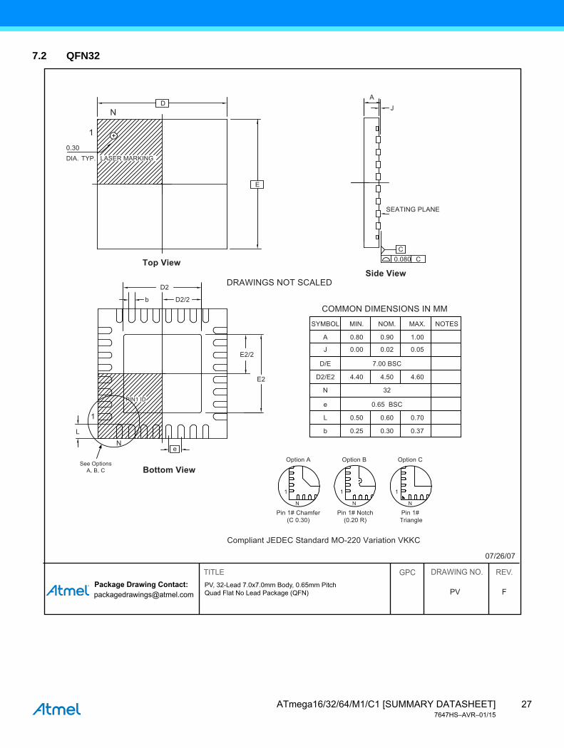
7.2 QFN32
Package Drawing Contact:[email protected]
GPC DRAWING NO. REV. TITLE
PV F
07/26/07
PV, 32-Lead 7.0x7.0mm Body, 0.65mm PitchQuad Flat No Lead Package (QFN)
Top View
Bottom View
Side View
D
0.30DIA. TYP. LASER MARKING
N
1
E
See OptionsA, B, C
1
N N N
1 1
Option A
Pin 1# Chamfer(C 0.30)
Pin 1# Notch(0.20 R)
Pin 1# Triangle
Option B Option C
0.080 CC
AJ
D2
D2/2
E2/2
PIN1 ID
E2
b
e
L
1
N
SEATING PLANE
DRAWINGS NOT SCALED
Compliant JEDEC Standard MO-220 Variation VKKC
COMMON DIMENSIONS IN MM
SYMBOL MIN. NOM. MAX.
A 0.80 0.90
0.02
1.00
D/E 7.00 BSC
L 0.50 0.60 0.70
b 0.25 0.30 0.37
D2/E2 4.40 4.50
N 32
e 0.65 BSC
4.60
J 0.00 0.05
NOTES
27ATmega16/32/64/M1/C1 [SUMMARY DATASHEET]7647HS–AVR–01/15
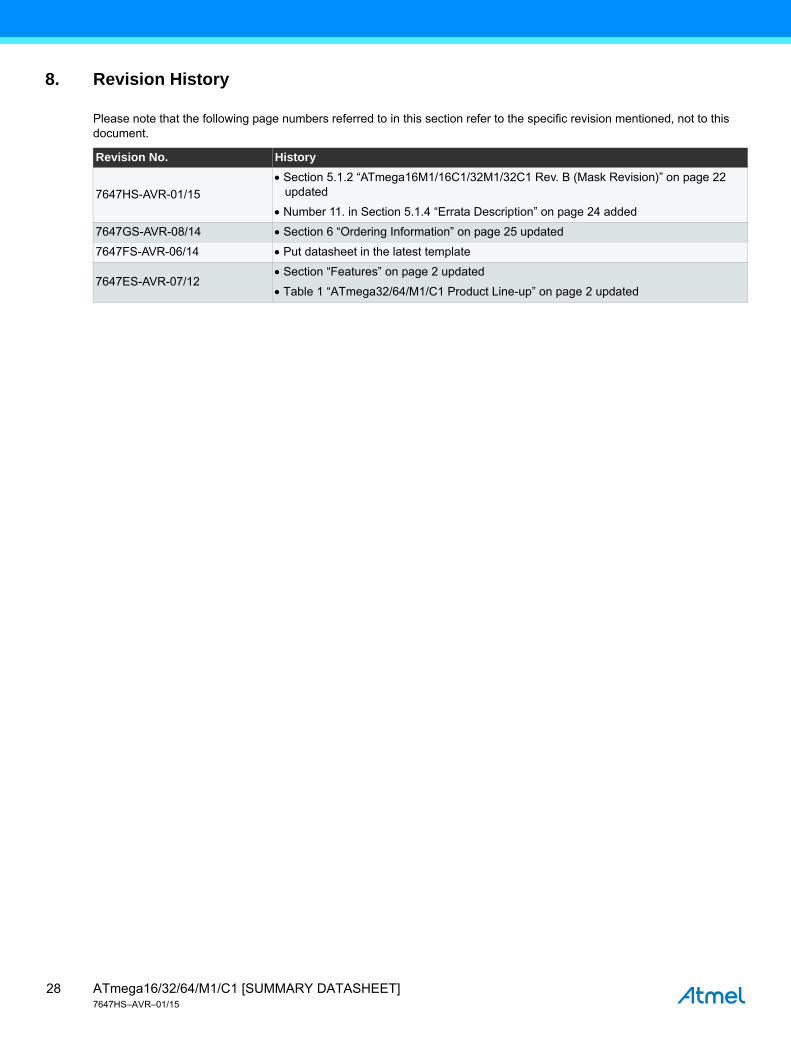
8. Revision History
Please note that the following page numbers referred to in this section refer to the specific revision mentioned, not to this document.
Revision No. History
7647HS-AVR-01/15
Section 5.1.2 “ATmega16M1/16C1/32M1/32C1 Rev. B (Mask Revision)” on page 22 updated
Number 11. in Section 5.1.4 “Errata Description” on page 24 added
7647GS-AVR-08/14 Section 6 “Ordering Information” on page 25 updated
7647FS-AVR-06/14 Put datasheet in the latest template
7647ES-AVR-07/12Section “Features” on page 2 updated
Table 1 “ATmega32/64/M1/C1 Product Line-up” on page 2 updated
ATmega16/32/64/M1/C1 [SUMMARY DATASHEET]7647HS–AVR–01/15
28

XX X XX XAtmel Corporation 1600 Technology Drive, San Jose, CA 95110 USA T: (+1)(408) 441.0311 F: (+1)(408) 436.4200 | www.atmel.com
© 2015 Atmel Corporation. / Rev.: 7647HS–AVR–01/15
Atmel®, Atmel logo and combinations thereof, Enabling Unlimited Possibilities®, AVR®, and others are registered trademarks or trademarks of Atmel Corporation in U.S. and other countries. Other terms and product names may be trademarks of others.
DISCLAIMER: The information in this document is provided in connection with Atmel products. No license, express or implied, by estoppel or otherwise, to any intellectual property rightis granted by this document or in connection with the sale of Atmel products. EXCEPT AS SET FORTH IN THE ATMEL TERMS AND CONDITIONS OF SALES LOCATED ON THEATMEL WEBSITE, ATMEL ASSUMES NO LIABILITY WHATSOEVER AND DISCLAIMS ANY EXPRESS, IMPLIED OR STATUTORY WARRANTY RELATING TO ITS PRODUCTSINCLUDING, BUT NOT LIMITED TO, THE IMPLIED WARRANTY OF MERCHANTABILITY, FITNESS FOR A PARTICULAR PURPOSE, OR NON-INFRINGEMENT. IN NO EVENTSHALL ATMEL BE LIABLE FOR ANY DIRECT, INDIRECT, CONSEQUENTIAL, PUNITIVE, SPECIAL OR INCIDENTAL DAMAGES (INCLUDING, WITHOUT LIMITATION, DAMAGESFOR LOSS AND PROFITS, BUSINESS INTERRUPTION, OR LOSS OF INFORMATION) ARISING OUT OF THE USE OR INABILITY TO USE THIS DOCUMENT, EVEN IF ATMEL HASBEEN ADVISED OF THE POSSIBILITY OF SUCH DAMAGES. Atmel makes no representations or warranties with respect to the accuracy or completeness of the contents of thisdocument and reserves the right to make changes to specifications and products descriptions at any time without notice. Atmel does not make any commitment to update the informationcontained herein. Unless specifically provided otherwise, Atmel products are not suitable for, and shall not be used in, automotive applications. Atmel products are not intended,authorized, or warranted for use as components in applications intended to support or sustain life.
SAFETY-CRITICAL, MILITARY, AND AUTOMOTIVE APPLICATIONS DISCLAIMER: Atmel products are not designed for and will not be used in connection with any applications wherethe failure of such products would reasonably be expected to result in significant personal injury or death (“Safety-Critical Applications”) without an Atmel officer's specific writtenconsent. Safety-Critical Applications include, without limitation, life support devices and systems, equipment or systems for the operation of nuclear facilities and weapons systems.Atmel products are not designed nor intended for use in military or aerospace applications or environments unless specifically designated by Atmel as military-grade. Atmel products arenot designed nor intended for use in automotive applications unless specifically designated by Atmel as automotive-grade.