atomistic simulation of the vapor deposition of ni/cu/ni ... · atomistic simulation of the vapor...
TRANSCRIPT

JOURNAL OF APPLIED PHYSICS VOLUME 87, NUMBER 1 1 JANUARY 2000
Atomistic simulation of the vapor deposition of Ni/Cu/Ni multilayers:Incident adatom angle effects
X. W. Zhou and H. N. G. WadleyDepartment of Materials Science, School of Engineering and Applied Science, University of Virginia,Charlottesville, Virginia 22903
~Received 8 March 1999; accepted for publication 21 September 1999!
Molecular dynamics simulations have been used to explore the effects of incident adatom angleupon the atomic scale structure of Ni/Cu/Ni multilayers grown by vapor deposition under controlledincident atom energy conditions. For incident atom energies of 1 eV or less, increasing the incidentangle increased interfacial roughness, resulted in void formation in the nickel layer, and intermixingat the interfaces between metal layers. The interfacial roughness that formed during low impactenergy oblique angle deposition was significantly reduced by substrate rotation during growth.However, rotation had no beneficial effects upon interfacial mixing. The use of a higher incidentatom energy~>5 eV/atom! resulted in flatter interfaces and eliminated voids under obliqueincidence conditions, but it also caused more severe interfacial mixing by an atomic exchangemechanism. When low~thermal! impact energies were used to deposit the first few monolayers ofeach new metal layer, intermixing by the exchange mechanism during subsequent hyperthermalenergy deposition could be significantly reduced. Using this modulated incident energy growthstrategy, films with little interfacial roughness and intermixing could be grown over a wide range ofincident angles with or without substrate rotation. ©2000 American Institute of Physics.@S0021-8979~00!01301-3#
k
lietrllye
esreleghd
si-u
sthmrkRbie
urionit
entny
etersbias
ndghnd-ul-
on
lorera-
md
in-ing.tifyRthaten-drfa-eryg,offin-er,nttion
rial
I. INTRODUCTION
Metal multilayers consisting of pairs of 50–70 Å thicferromagnetic layers that sandwich a thin~10–30 Å! copperlayer can exhibit giant magnetoresistance~GMR!.1–28 GMRmaterials undergo large~5%–80% or more! reductions intheir electrical resistance when a magnetic field is appbecause of changes in the spin dependent elecscattering.1,3 GMR materials are becoming technologicaimportant; they have already been used for magnetic fisensors in the read heads of hard disk drives,29–31 and arebeing developed for nonvolatile magnetic random accmemories.31 These applications have spurred intense intein the design of economical deposition processes capabproducing thermally stable GMR materials that exhibit hiGMR ratios~defined as the maximum resistance changevided by the resistance at magnetic saturation! with low satu-ration magnetic fields.
GMR multilayers can be created by many phycal vapor deposition techniques including molecelar beam epitaxy,11–13,27 various sputter depositionmethods,6–8,14–28,32,33as well as ion-beam and ion-beam asisted deposition.34 Each process results in multilayers wiwidely different GMR behavior presumably resulting froslightly different atomic scale structures. While much woremains to fully determine the relationship between GMproperties and atomic scale structure, it appears that theGMR properties are obtained when the roughness of theterfaces and the degree of mixing between the ferromagnand the conductive layers are minimized. These structattributes of the films are strongly affected by depositconditions such as the substrate temperature, the depos
5530021-8979/2000/87(1)/553/11/$17.00
Downloaded 04 Apr 2005 to 128.143.35.28. Redistribution subject to AIP
don
ld
sstof
i-
-
-
estn-tical
ion
rate, the depositing atoms’ incident energy, their incidangle, etc. These conditions are in turn controlled by maother deposition method dependent processing param~such as chamber pressure, target–substrate distance,voltage, and so on!. The selection of the best process aoptimization of the process conditions for depositing hiperformance GMR multilayers requires a better understaing of the fundamental relationship between a deposited mtilayer’s GMR controlling nanostructure and its depositiconditions.
Molecular dynamics methods have been used to expthe mechanisms of surface roughening during low tempeture film growth35 and investigate the role of incident atoenergy upon surface modification.36 These studies indicatethat surface roughness increased with film thickness, andcreases in incident atom energy promoted surface flattenMolecular dynamics simulations have also begun to idenprocess conditions that are likely to result in good GMproperties.37 For normal incident angle atom deposition, bothe interfacial roughness and the extent of intermixinginterfaces were found to depend upon the incident atomergy. High~e.g., above 5 eV! incident atom energies lowerethe atomic scale interfacial roughness but promoted intecial mixing by an exchange mechanism. Conversely, vlow ~;0.1 eV! incident atom energies reduced intermixinbut resulted in films with rough interfaces. The best tradebetween roughness and intermixing was found when ancident energy of 1–2 eV was used for deposition. Howevthe model indicated that significant further improvemecould be achieved by using a modulated energy depositechnique in which low~;0.1 eV! incident energies wereused to deposit the first few monolayers of a new mate
© 2000 American Institute of Physics
license or copyright, see http://jap.aip.org/jap/copyright.jsp

teniogu
mptr
puen
00neosreanos
llegue
nm.oc-s tsepoindifoade
cialndus
ave
-t offor
An
so
m-ho-
re
nd-at
his
om
ge
ntb-
554 J. Appl. Phys., Vol. 87, No. 1, 1 January 2000 X. W. Zhou and H. N. G. Wadley
layer and higher energies~e.g., 5 eV! were used for itscompletion.
Energy modulation appears possible with most sputing processes,38 but may be most easily implemented in iobeam deposition systems. A schematic illustration of anbeam deposition system is shown in Fig. 1. An ion beamis used to generate a high energy~;0.1–2 keV! Ar1, Kr1,or Xe1 ion beam which is directed at a target~e.g., copper orpermalloy!. Ion bombardment of the target results in atosputtering from its surface. These metal atoms then progate toward a substrate and are deposited on the subssurface. Recent molecular dynamics simulations of the stering of nickel by argon ions indicated that the averageergy of the emitted nickel atoms increases from;4 to ;13eV as the argon ion energy is increased from 50 to 1eV.39 Controlling ion gun voltage therefore provides omethod for manipulating the adatom energy during deption. Collisions with the background gas atoms can alsoduce the energy of the sputtered atoms as they are trported from the target to the substrate. The probability~energy loss! collisions increases with the background presure PB or the target–substrate distancedTS. The impactenergy of depositing atoms can therefore also be controby selecting an appropriate combination of the ion beamacceleration voltage, background pressure, and targsubstrate distance.
Both geometric constraints within multielement iobeam deposition systems and gas phase scattering canit difficult to achieve normal~u50°! impact angle depositionExperiments40 and recent molecular dynamics simulationsthin film deposition41–43have shown that increasing the fration of deposited atoms with oblique incident angles leada rougher growth surface. Collimation methods can be uto control the angular dispersion, but it results in lower desition rates and can be an undesirable source of contamtion. In some deposition systems, substrate rotation is usereduce roughness and to improve surface thickness unmity. However, this can also be a significant source of pticle contamination. Here, the molecular dynamics moused earlier to investigate energy dependent deposition37 has
FIG. 1. Schematic illustration of an ion beam deposition system~the trans-lation energy of sputtered metal atoms increases with acceleration voltathe ion beam gun in the 50–1000 V range!.
Downloaded 04 Apr 2005 to 128.143.35.28. Redistribution subject to AIP
r-
nn
a-atet--
0
i--s-f-
dnt–
ake
f
od-a-tor-
r-l
been extended to explore the dependence of interfaroughness and intermixing on the flux incident angle asubstrate rotation. To simplify comparisons with previowork, the growth of a model Ni/Cu/Ni multilayer in the@111# direction has been analyzed.
II. COMPUTATION METHOD
Details of the molecular dynamics model used here hbeen described in an earlier paper.37 Briefly, a Cu–Ni alloyembedded atom method potential44 was used to calculate interaction forces between the atoms. This potential was cuat 4.95 Å which is larger than the third nearest neighbdistance, yielding a realistic description of the fcc crystal.identical crystal geometry to that previously employed37 wasused for the calculation. A nickel substrate was orientatedthat itsx, y, andz edges were aligned in the@112̄#, @111#, and@11̄0# directions, respectively. To achieve reasonable coputation efficiency, the size of the substrate crystal was csen to contain 120 (224)̄ planes in thex direction, three~111!planes in they direction, and 12~220! planes in thez direc-tion ~see Fig. 2!. The effects of the small crystal size weminimized by using periodic boundary conditions in thexandz directions so that the crystal can be viewed as exteing infinitely in these two directions. It should be noted ththez length of the substrate cell was about 14.9 Å. While tis approximately one fourth of thex length of the cell, it iswell above the cutoff distance of the potential.
By imposing a free boundary condition at the top~y!surface and using a fixed boundary condition for the bott~y! surface, growth in they direction could be simulated.37
of
FIG. 2. Atomic structure of Ni/Cu/Ni multilayers as a function of incideangleu at a fixed incident energy of 1.0 eV, grown with a stationary sustrate: ~a! u50°, ~b! u520°, ~c! u535°, ~d! u540°, ~e! u550°, and ~f!u555°.
license or copyright, see http://jap.aip.org/jap/copyright.jsp
sl.
d,loen,-uc
-e
thow
thred
poteo,aaro-
ese
ofingg
su.ao
ths
enhefilu
e
coer
ony-
60°tiveentsentms.ter-
ionial
andel
gle,ande 2er-y,re-
dentr onr aater., thepergh-r forthe
555J. Appl. Phys., Vol. 87, No. 1, 1 January 2000 X. W. Zhou and H. N. G. Wadley
Multilayer deposition was simulated by alternatively depoiting about 20 Å of copper followed by about 20 Å of nickeThe incident atom energyEi as well as its incident angleu~defined as the angle between the incoming direction of atoms and the surface normal!, as shown in Figs. 1 and 2were simply implemented by assigning an appropriate veity vector to each atom. To uniquely define a three dimsional incident direction relative to a stationary substrateuwas initially set in thex–y plane. For some of the simulations, the effect of substrate rotation was examined. In scases, the azimuth anglec ~see Fig. 1!, was varied~at theprescribed rotation rate! during deposition while the substrate remained fixed. It should be pointed out that the usa relatively small thickness~;15 Å! in the z direction withthe periodic boundary condition would underestimatesignificance of the shadowing and prevent the formationlong wavelength roughness along this direction. Becauseonly analyzed the roughness in thex direction, theroughness–rotation trends are likely to be unaffected byapproximation. As in previous work, all simulations weconducted at a fixed substrate temperature of 300 K anfixed deposition rate of 10 nm/ns. The use of this high desition rate was necessary in order to deposit an appropriathick sample within the computational time constraint of mlecular dynamics.41 Under a high rate deposition conditionthermal diffusion events on the microsecond time scalenot captured in the simulation. The simulation resultstherefore strictly valid for low temperature deposition prcesses where thermally activated diffusion is negligible.
To quantify the dependence of the interfacial roughnupon incident angle, a roughness parameter needs to bfined. In experiments, the surface roughness parameterr 2 isusually defined as the average deviation of the surface prfrom the mean surface height over a selected area or lescale of micrometer.32 However, problems arose when usinthe average deviation of surface atoms from the meanface height to calculater 2 for a given atomic configurationFor instance, different sections of a nonplanar surfaceusually associated with different crystallographic planesdifferent atomic densities. Hence, the deviation frommean surface height averaged over all surface atoms estially measures different sections of the surface with differweighing factors. Because the mean height lies somewbetween the highest and lowest point on the surface pror 2 may also incorrectly specify a higher roughness for a sface containing one high terrace than for a~rougher! surfacecomposed of many asperities~as long as their heights arwithin the height difference of the high and low terraces!. Ithas been shown that the surface roughness of atomicfigurations is better represented by a roughness parametr 1
defined as the average aspect ratio of surface asperities.37 Forsurfaces with a sinoidal roughness, ther 1 parameter can bescaled to an equivalent value ofr 2 if the average width ofasperities is known.37
III. INCIDENT ANGLE EFFECTS
A. Atomic configurations
To investigate the effect of incident atom direction upatomic scale structure, the deposition of Ni/Cu/Ni multila
Downloaded 04 Apr 2005 to 128.143.35.28. Redistribution subject to AIP
-
a-
c--
h
of
efe
is
a-ly
-
ree
sde-
leth
r-
ref
een-tree,r-
n-
ers was simulated using incident atom angles from 0° toand a fixed incident atom energy of 1.0 eV. Representaexamples of the atomic configurations for selected incidangles are shown in Fig. 2, where dark spheres reprenickel atoms while the lighter ones represent copper atoIt is apparent that the roughness of the interfaces and inmixing in these multilayers was sensitive to the depositangle. Oblique angle deposition produced high interfacroughness~especially at the copper on nickel interface!.When the incident angle was increased to about 40°beyond, voids also formed during the deposition of nicklayers. The size of these voids increased with incident anand extended through the entire nickel layer thicknessinto the copper layer for the highest incident angles. Figuralso indicates that mixing of the two materials at their intfaces increased with incident angle. As in our earlier stud37
copper atoms tended to mix in the nickel layers more fquently than vice versa.
B. Interfacial roughness
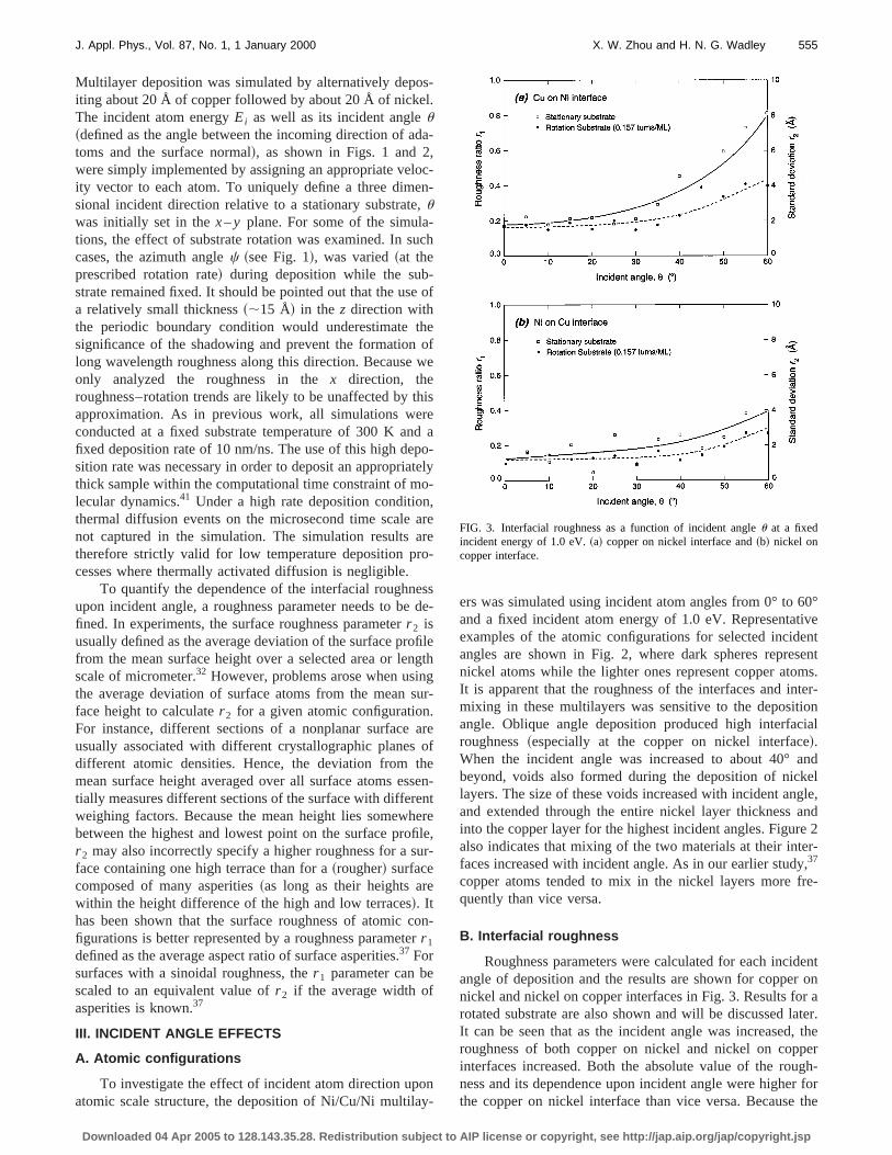
Roughness parameters were calculated for each inciangle of deposition and the results are shown for coppenickel and nickel on copper interfaces in Fig. 3. Results forotated substrate are also shown and will be discussed lIt can be seen that as the incident angle was increasedroughness of both copper on nickel and nickel on copinterfaces increased. Both the absolute value of the rouness and its dependence upon incident angle were highethe copper on nickel interface than vice versa. Because
FIG. 3. Interfacial roughness as a function of incident angleu at a fixedincident energy of 1.0 eV.~a! copper on nickel interface and~b! nickel oncopper interface.
license or copyright, see http://jap.aip.org/jap/copyright.jsp

cres
gpethi/athhash
errt
ar
in
aieaclearnc
os
in
hurrva
ye5e
naces
ih
coe
gh
sube
d
on
pth
rac-Thein-
meeen-
be-the
at
theeep-
nceceesssed.s,
ther-igh
e1.0
556 J. Appl. Phys., Vol. 87, No. 1, 1 January 2000 X. W. Zhou and H. N. G. Wadley
copper on nickel interface was always the last interfaformed in the system shown in Fig. 3, it could be conjectuthat its higher roughness was caused by an increase offace roughness with increasing thickness.35 To clarify this,additional simulations were conducted by first depositinnickel layer on the copper substrate followed by a coplayer and a second nickel layer. Again, the copper onnickel interface was rougher. Also, the growth of the NCu/Ni multilayers shown in Fig. 3 was continued to formsecond nickel on copper interface. The results revealedwhile the second nickel on copper interface was rougher tthe first one~due to an increase of roughness with thicknes!,it was still smoother than the copper on nickel interface. Thigher roughness of the copper on nickel interface was thfore a material effect and did not depend upon the ordethe deposition sequence. Figure 3 also indicates thatroughness of the copper on nickel interface was particulsensitive to the incident angle whenu.40°. By comparingwith Fig. 2, it can be seen that this coincides with the begning of the formation of voids in the nickel layer.
C. Roughening mechanisms
Molecular dynamics simulations of deposition at normincidence indicated that adatoms with low incident energfrequently attached to the top and the sidewalls of surfasperities.37 When all atoms have the same incident angshadowing can then exclude the incoming atoms from pof the valleys between the asperities, resulting in an enhament of the surface roughness.37 This phenomenon is anusual explanation for the high surface roughness and vcontent during oblique angle deposition of pure metal filmand has been analyzed for two dimensional growth.43
Complexities are introduced when growth occursthree dimensions and/or different materials~with differentmobilities! are sequentially deposited. To investigate tevolution of interfacial roughness and void morphology ding oblique angle deposition, additional simulations weconducted using larger crystals to allow detailed obsertions of the three dimensional growth process. Figureshows representative stages of the growth of a multiladeposited with 1.0 eV adatoms incident at an angle of 5To simplify visualization of the internal voids, parts of thcrystal have been removed after the simulation.
During the initial stage of deposition, atoms were radomly deposited on the surface and formed small surfasperities. Under collimated oblique angle condition, thasperities blocked the incoming flux of adatoms, resultingan unreachable shadowed region behind each asperity. Wfurther deposition caused the unshadowed regions totinuously grow, growth in shadowed region was slower bcause it required the surface migration of atoms from neiboring regions. Because a high deposition rate was usedthe simulations, the vertical deposition rate exceeded theface~diffusion! transport rate. The shadowed region thencame large valleys such as the region with a profileRx inFig. 4~b!. The valley width along thex direction ~in whichshadowing occurred! scaled with (h1–h2) tan(u), whereh1
and h2 are the heights of the two walls bounding the sha
Downloaded 04 Apr 2005 to 128.143.35.28. Redistribution subject to AIP
edur-
are
atn
ee-ofhely
-
lse,tse-
id,
e-e-
4r
°.
-eenilen---
forr--
-
owed region in thex direction. Because the shadowed regiwas initially nucleated on a flat surface,h1–h2 was smalland hence, the width of the valley in thex direction was alsosmall ~see the surface profileRx!. Extension of the valley inthez direction was seen to accompany the growth in its dewhen the flux incident angleu ~in thex–y plane! was large.This was caused by the lateral growth~in the z direction! ofthe shadowing asperities due to the long range atomic atttions between surface atoms and nearby vapor atoms.surface valley then became a local trench whose depthcreased as the deposition time increased. At tit5450 ps, Fig. 4~c!, continued deposition of atoms on thtrench lip caused a bulge at the trench opening. Atoms evtually became sufficiently close that the attractive forcestween surface and vapor atoms caused a pinch-off oftrench, resulting in the trapping of a void in the filmt5550 ps, Fig. 4~d!. Figure 4~d! shows that the void formedwas extended in thez direction, but was relatively narrow inthex direction. Although surface roughness developed inz direction due to the randomness of atom arrivals, no dvalleys were observed in this direction@see the surface profile Rz in Fig. 4~b!#.
Increasing the incident angle increased the significaof shadowing and reduced the probability that surfatrenches would be filled. Consequently, surface roughnand void size increased as the incident angle was increaSince valleys can be filled by the migration of surface atomsurface roughness and void content can be reduced bymally activated surface diffusion when temperature is h
FIG. 4. Three dimensional illustration of void formation during obliquangle deposition at an incident angle of 55° and an incident energy ofeV: ~a! t50 ps, ~b! t5350 ps,~c! t5450 ps, and~d! t5550 ps.
license or copyright, see http://jap.aip.org/jap/copyright.jsp
ngb
iondi
eotugfo
de
d
yepebit
inhel tetg
hlygan
at
ngeen-nsu-thinTheandentergy
x-
im-
inive
hisolu-ce
face
t
557J. Appl. Phys., Vol. 87, No. 1, 1 January 2000 X. W. Zhou and H. N. G. Wadley
or deposition rate is low. If the energy of the depositiatoms is high, the shadowed regions can also be filledimpact induced diffusion mechanisms.45,46 This is the domi-nant mechanism of surface transport active in the simulatreported here. Because the extent of surface migrationpends on atom mobility and the mobility of copper atomsgreater than that of nickel atoms,47 the roughness on thnickel surface is less likely to be flattened. As a result, broughness and the incident angle dependence of the roness were higher for the copper on nickel interface thanthe nickel on copper interface, and voids preferentiallyveloped in the nickel layer.
D. Interfacial mixing
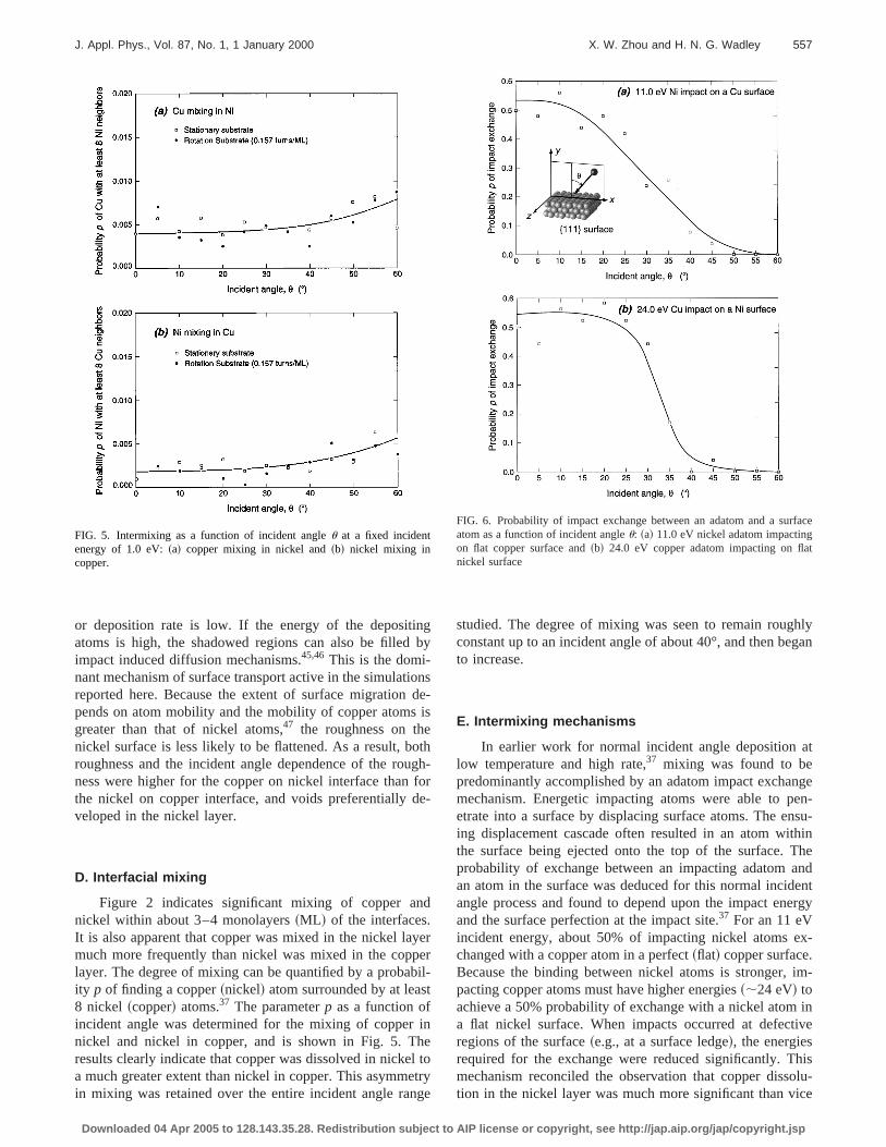
Figure 2 indicates significant mixing of copper annickel within about 3–4 monolayers~ML ! of the interfaces.It is also apparent that copper was mixed in the nickel lamuch more frequently than nickel was mixed in the coplayer. The degree of mixing can be quantified by a probaity p of finding a copper~nickel! atom surrounded by at leas8 nickel ~copper! atoms.37 The parameterp as a function ofincident angle was determined for the mixing of coppernickel and nickel in copper, and is shown in Fig. 5. Tresults clearly indicate that copper was dissolved in nickea much greater extent than nickel in copper. This asymmin mixing was retained over the entire incident angle ran
FIG. 5. Intermixing as a function of incident angleu at a fixed incidentenergy of 1.0 eV:~a! copper mixing in nickel and~b! nickel mixing incopper.
Downloaded 04 Apr 2005 to 128.143.35.28. Redistribution subject to AIP
y
se-s
hh-r-
rrl-
orye
studied. The degree of mixing was seen to remain rougconstant up to an incident angle of about 40°, and then beto increase.
E. Intermixing mechanisms
In earlier work for normal incident angle depositionlow temperature and high rate,37 mixing was found to bepredominantly accomplished by an adatom impact exchamechanism. Energetic impacting atoms were able to petrate into a surface by displacing surface atoms. The eing displacement cascade often resulted in an atom withe surface being ejected onto the top of the surface.probability of exchange between an impacting adatoman atom in the surface was deduced for this normal incidangle process and found to depend upon the impact enand the surface perfection at the impact site.37 For an 11 eVincident energy, about 50% of impacting nickel atoms echanged with a copper atom in a perfect~flat! copper surface.Because the binding between nickel atoms is stronger,pacting copper atoms must have higher energies~;24 eV! toachieve a 50% probability of exchange with a nickel atoma flat nickel surface. When impacts occurred at defectregions of the surface~e.g., at a surface ledge!, the energiesrequired for the exchange were reduced significantly. Tmechanism reconciled the observation that copper disstion in the nickel layer was much more significant than vi
FIG. 6. Probability of impact exchange between an adatom and a suratom as a function of incident angleu: ~a! 11.0 eV nickel adatom impactingon flat copper surface and~b! 24.0 eV copper adatom impacting on flanickel surface
license or copyright, see http://jap.aip.org/jap/copyright.jsp
558 J. Appl. Phys., Vol. 87, No. 1, 1 January 2000 X. W. Zhou and H. N. G. Wadley
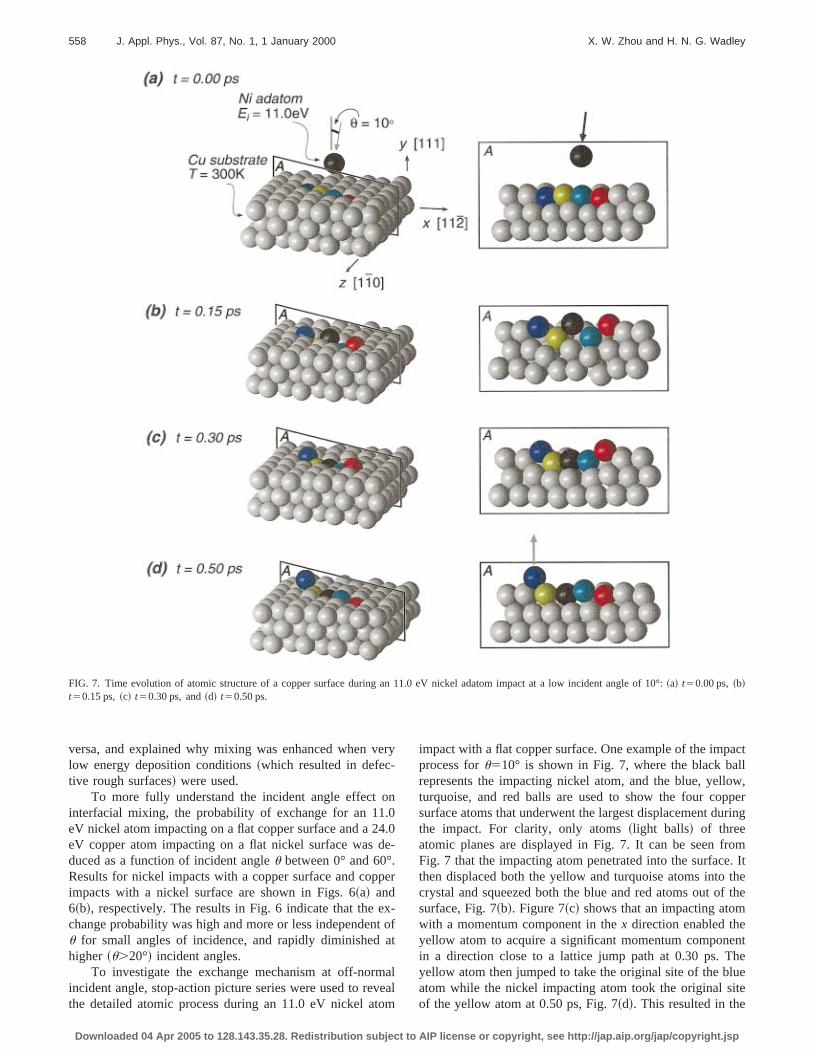
FIG. 7. Time evolution of atomic structure of a copper surface during an 11.0 eV nickel adatom impact at a low incident angle of 10°:~a! t50.00 ps,~b!t50.15 ps,~c! t50.30 ps, and~d! t50.50 ps.
e
on.04de.p
xta
aveo
actllow,perring
om. Itthef the
entheueite
versa, and explained why mixing was enhanced when vlow energy deposition conditions~which resulted in defec-tive rough surfaces! were used.
To more fully understand the incident angle effectinterfacial mixing, the probability of exchange for an 11eV nickel atom impacting on a flat copper surface and a 2eV copper atom impacting on a flat nickel surface wasduced as a function of incident angleu between 0° and 60°Results for nickel impacts with a copper surface and copimpacts with a nickel surface are shown in Figs. 6~a! and6~b!, respectively. The results in Fig. 6 indicate that the echange probability was high and more or less independenu for small angles of incidence, and rapidly diminishedhigher ~u.20°! incident angles.
To investigate the exchange mechanism at off-normincident angle, stop-action picture series were used to rethe detailed atomic process during an 11.0 eV nickel at
Downloaded 04 Apr 2005 to 128.143.35.28. Redistribution subject to AIP
ry
.0-
er
-oft
lal
m
impact with a flat copper surface. One example of the impprocess foru510° is shown in Fig. 7, where the black barepresents the impacting nickel atom, and the blue, yellturquoise, and red balls are used to show the four copsurface atoms that underwent the largest displacement duthe impact. For clarity, only atoms~light balls! of threeatomic planes are displayed in Fig. 7. It can be seen frFig. 7 that the impacting atom penetrated into the surfacethen displaced both the yellow and turquoise atoms intocrystal and squeezed both the blue and red atoms out osurface, Fig. 7~b!. Figure 7~c! shows that an impacting atomwith a momentum component in thex direction enabled theyellow atom to acquire a significant momentum componin a direction close to a lattice jump path at 0.30 ps. Tyellow atom then jumped to take the original site of the blatom while the nickel impacting atom took the original sof the yellow atom at 0.50 ps, Fig. 7~d!. This resulted in the
license or copyright, see http://jap.aip.org/jap/copyright.jsp

cx
acge
eaenino-ida
to
t tei
eig-fi-to.tlin-
entrfa-arn-ar-
re-foring
ureci-theFig.ig.
eVin-forse-hin-
tedre-
ichntoo-there-
ing
559J. Appl. Phys., Vol. 87, No. 1, 1 January 2000 X. W. Zhou and H. N. G. Wadley
ejection of the blue atom upwards onto the top of the surfaDuring this process, the turquoise and the red atoms relato their original surface site.
Similar stop-action picture series analysis for the impof a flat copper surface by an 11.0 eV nickel atom at larincident angles~e.g., u560°! indicated that the nickel im-pacting atom was less likely to penetrate the surface. Instit usually skipped on the surface, resulting in biasdiffusion.45 Clearly, exchange was significant at low incideangles, and the peak exchange rate occurred when thedent direction is slightly off the surface normal which prvided the lateral momentum for a lattice jump. The rapdecline in exchange probability at high incident angle wthe result of a transition from adatom exchange to adaskipping in the direction of incidence.45
The impacts analyzed above at first sight suggest thaintermixing should decrease with incident angle. Howevthe opposite trend was observed: Fig. 5 shows that interming increased with incident angle. This occurred becauslarge incident angles, the surface roughness was very hWhile the nominal incident angle~defined as the angle between the incident direction and the average normal omacroscopic scale surface! was large, the average local incdent angle had decreased because a large fraction of adanow impacted the sides of valleys on the rough surfaceaddition, the exchange probability increased significanwith surface roughness which, at low incident energy,creased withu. The net effect was an intermixing that increased with incident angle.
FIG. 8. Interfacial roughness as a function of incident energyEi at a fixedincident angle of 50°:~a! copper on nickel interface and~b! nickel on copperinterface.
Downloaded 04 Apr 2005 to 128.143.35.28. Redistribution subject to AIP
e.ed
tr
d,dtci-
sm
her,x-ath.
a
msIny-
IV. INCIDENT ENERGY DEPENDENCE
The simulations above were conducted with an incidenergy of 1.0 eV and the results suggested that both intecial roughness and intermixing were minimized with a nenormal incident angle deposition. This significantly costrains the design of a vapor deposition technology. An elier study37 indicates that high adatom incident energiessult in smoother surfaces. To evaluate its significanceoblique deposition, the interfacial roughness and the mixprobability as a function of incident energy foru550° werecalculated and the results are shown in Figs. 8 and 9. Fig8 indicates that the roughness initially decreased with indent energy for both interfaces. This trend continued forcopper on nickel interface up to at least 6 eV as seen in8~a!. The roughness of the nickel on copper interface, F8~b!, exhibited a minimum at an incident energy around 3and then increased with incident energy. The apparentcrease in roughness of the nickel on copper interfaceincident energy above 3.0 eV was an anomalous conquence of the mixing of copper in the nickel layer whiccreated an increasingly diffuse interface as the energycreased. A detailed examination of the simulations indicathat the initial decrease in roughness of both interfacessulted from impact energy induced surface diffusion whpromoted step flow growth and the transport of atoms ithe shadowed regions.37 Because copper atoms are more mbile than nickel atoms, the copper surface was flatter thannickel surface and the nickel on copper interface was thefore smoother. Figure 9 summarizes the interfacial mix
FIG. 9. Intermixing as a function of incident energyEi at a fixed incidentangle of 50°:~a! copper mixing in nickel and~b! nickel mixing in copper.
license or copyright, see http://jap.aip.org/jap/copyright.jsp

kiniea
ob
ioani-lyglR
b-in
thwtth
glix
momu
Mw
poiio
rfa
the.01
be-
g,nntwsro-t ab-
beratergy
l onr arob-o-po-ofess
andi-gh-d ase-astedgle.lsoof
tiva-
ed
o
inove
ateg
at a
560 J. Appl. Phys., Vol. 87, No. 1, 1 January 2000 X. W. Zhou and H. N. G. Wadley
observations. It can be seen that both copper mixing in nicand nickel mixing in copper increased continuously withcident energy over the entire incident energy range studThis resulted from an increased exchange probabilityhigher incident energy and is consistent with the resultstained for the normal incident angle deposition.37
These results indicate that while high energy depositimproves interfacial roughness, it also results in significinterlayer mixing. Conversely, low energy deposition minmizes intermixing, but it results in rough interfaces. Clearthe use of a high energy alone during high incident andeposition is unlikely to produce high quality GMmultilayer structures.
V. SUBSTRATE ROTATION
High interfacial roughness and intermixing during olique angle deposition have been correlated with shadoweffects. Changing the direction of the incoming flux wirespect to the crystal by substrate rotation during groshould significantly reduce shadowing and hence offerspromise of improved interfacial roughness for oblique andeposition at a sufficiently low energy to induce no interming.
A. Rotation rate behavior
To explore rotation effects, a series of molecular dynaics calculations were conducted at a fixed incident atangle of 50° and an incident energy of 1.0 eV using simlated substrate rotation rates that varied from 0.001 turns/to 0.200 turns/ML. Selected atomic configurations are shoin Fig. 10. It can be seen that for low energy oblique desition, increasing the substrate rotation rate reduced theterfacial roughness and eliminated the formation of voidsthe nickel layer. The dependence of interfacial roughnesssubstrate rotation rate is summarized in Fig. 11. The inte
FIG. 10. Atomic structure of Ni/Cu/Ni multilayers as a function of substrrotation rate at a fixed incident energy of 1.0 eV and a fixed incident anof 50°: ~a! 0.001 turns/ML,~b! 0.003 turns/ML,~c! 0.009 turns/ML, and~d!0.196 turns/ML.
Downloaded 04 Apr 2005 to 128.143.35.28. Redistribution subject to AIP
el-d.t-
nt
,e
g
he
e-
-
-Ln-n-nn-
cial roughness is seen to initially decrease rapidly assubstrate rotation rate was increased from 0 to about 0turns/ML. It then became insensitive to the rotation rateyond about 0.01 turns/ML.
Substrate rotation was not found to improve intermixin~Figs. 5 and 9!. The beneficial effect of substrate rotatioupon roughness is especially significant for high incideangle and low energy deposition conditions. Figure 3 shothe improvement in interfacial roughness by a substratetation rate of 0.157 turns/ML for various incident angles alow incident energy of 1.0 eV. The combined effect of sustrate rotation and incident energy upon roughness canseen in Fig. 8. It shows that the beneficial effects of substrotation became progressively smaller as the incident enewas increased. It also shows that the benefits for a nickecopper interface were significantly smaller than those focopper on nickel interface. These occurred because the pability of forming surface asperities during stationary depsition was reduced by either a high incident energy or desition of high mobility copper. Rotation was thereforemost benefit when other processes for diminishing roughnwere the least effective.
VI. DISCUSSION
The results above indicate that interfacial roughnessintermixing of Ni/Cu/Ni multilayers increased with the incdent angle of adatoms during deposition. Interfacial rouness was inherited from the surface roughness that formea result of shadowing at oblique angles of incidence. Bcause the probability for impact induced exchange whigher on a rougher surface, the intermixing was correlawith the surface roughness and increased with incident anThe surface roughness and the extent of intermixing adepended on the activation energies for surface diffusioneach element deposited. For copper, which has lower action energies for surface diffusion than nickel,47 the surfaceshadowed regions were readily filled through impact inducatom diffusion. As a result, copper surfaces~and thus nickelon copper interfaces! were relatively smooth compared tnickel surfaces~and therefore copper on nickel interfaces!.For similar reasons, the formation of voids occurred firstthe nickel layer as the incident angle was increased to ab
le
FIG. 11. Interfacial roughness as a function of substrate rotation ratefixed incident energy of 1.0 eV and a fixed incident angle of 50°.
license or copyright, see http://jap.aip.org/jap/copyright.jsp
thhowngcr
esudTiegNtiothiofled0.
ndn
wa
lieioounenrrghple
gy,-
s aryent
561J. Appl. Phys., Vol. 87, No. 1, 1 January 2000 X. W. Zhou and H. N. G. Wadley
about 40°. It was also apparent that copper mixing intonickel layer was much more significant than vice versa. Tarose because the cohesive energy of copper atoms is lthan that of nickel atoms. As a result, a nickel impactiatom is more likely to penetrate a copper surface and ejecopper atom onto the top of the copper surface than theverse case where a copper atom impacts a nickel surfac
Increasing the incident atom energies was a successtrategy for flattening the interfaces grown under obliqangle conditions. However, it also caused significant adtional intermixing by an atomic exchange mechanism.reduce this mechanism of intermixing, incident energmust be kept below about 1.0 eV, but this results in rouinterfaces especially at oblique angles of incidence.single energy deposition exists that results in the deposiof the high quality interfaces when the incident angle offlux is high. Substrate rotation during low energy depositwas found to reduce shadowing effects and resulted ininterfaces. Voids in the nickel layer were also eliminatwhen the substrate rotation rate exceeded aboutturns/ML ~3.6°/ML!. However, rotation did not significantlyreduce intermixing for oblique angle depositions,~Figs. 5and 9!. While the combination of interfacial roughness aintermixing obtained using substrate rotation during low eergy oblique angle depositions was improved, the resultstill far from perfection~see, for example, Fig. 10!.
One other growth strategy can be explored. In earwork37 it was shown that a modulated energy depositmethod significantly reduced interfacial roughness withcausing intermixing for a normal incident angle depositioIn this approach, the first few monolayers of a new elemwere deposited at a low incident energy and the remaindethat material was then deposited at a high incident eneThe low initial energy prevented intermixing while the higenergy resulted in surface flattening. To investigate thetential benefit of energy modulation during oblique ang
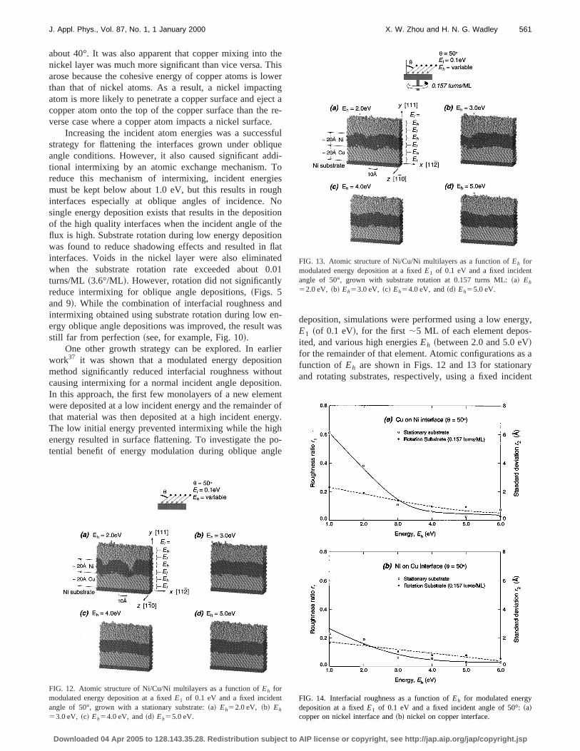
FIG. 12. Atomic structure of Ni/Cu/Ni multilayers as a function ofEh formodulated energy deposition at a fixedE1 of 0.1 eV and a fixed incidentangle of 50°, grown with a stationary substrate:~a! Eh52.0 eV, ~b! Eh
53.0 eV, ~c! Eh54.0 eV, and~d! Eh55.0 eV.
Downloaded 04 Apr 2005 to 128.143.35.28. Redistribution subject to AIP
eis
er
t ae-.fulei-oshon
enat
01
-s
rnt.t
ofy.
o-
deposition, simulations were performed using a low enerE1 ~of 0.1 eV!, for the first;5 ML of each element deposited, and various high energiesEh ~between 2.0 and 5.0 eV!for the remainder of that element. Atomic configurations afunction of Eh are shown in Figs. 12 and 13 for stationaand rotating substrates, respectively, using a fixed incid
FIG. 13. Atomic structure of Ni/Cu/Ni multilayers as a function ofEh formodulated energy deposition at a fixedE1 of 0.1 eV and a fixed incidentangle of 50°, grown with substrate rotation at 0.157 turns ML:~a! Eh
52.0 eV, ~b! Eh53.0 eV, ~c! Eh54.0 eV, and~d! Eh55.0 eV.
FIG. 14. Interfacial roughness as a function ofEh for modulated energydeposition at a fixedE1 of 0.1 eV and a fixed incident angle of 50°:~a!copper on nickel interface and~b! nickel on copper interface.
license or copyright, see http://jap.aip.org/jap/copyright.jsp

isinh
t-th
ssub
ts
nc
thbc
he
ngretio
igrsfgrfr
n ofiev-
bylts
vedion
mi-
re
ex-the.
ngin-
of
erss
esson,
t
562 J. Appl. Phys., Vol. 87, No. 1, 1 January 2000 X. W. Zhou and H. N. G. Wadley
angle of 50° and a rotation rate of 0.157 turns/ML. Thstrategy clearly improved both interfacial roughness andtermixing. The functional dependence of interfacial rougness and intermixing uponEh were calculated and are ploted in Figs. 14 and 15. It can be seen that increasingvalue ofEh significantly improved both interfacial roughneand intermixing. Furthermore, the beneficial effects of sstrate rotation were most significant at relatively lowEh val-ues. Above anEh of about 3.0 eV, rotation had little benefifor roughness or intermixing. These observations are a reof the effectiveness of the modulated energy strategyeliminating surface roughness even at high angles of idence.
To determine the incident angle range over whichbeneficial effects of modulated energy deposition canachieved, additional simulations were conducted using indent angles between 0° and 60°, anE1 of 0.1 eV, and anEh
of 5.0 eV, for both stationary and rotating substrates. Tresults are shown in Figs. 16 and 17. They indicate that vlow levels of both interfacial roughness and intermixiwere present over the entire incident angle range exploThey also show that no beneficial effect of substrate rotawas detectable.
These results provide significant guidance for the desand optimization of a growth approach for GMR multilayeToday, two competing deposition techniques are usedsynthesizing the high performance GMR multilayers: rf manetron ~or diode! sputtering and ion beam deposition. Insputtering systems, sputtered atoms must be transpo
FIG. 15. Intermixing as a function ofEh for modulated energy deposition aa fixedE1 of 0.1 eV and a fixed incident angle of 50°:~a! copper mixing innickel and~b! nickel mixing in copper.
Downloaded 04 Apr 2005 to 128.143.35.28. Redistribution subject to AIP
--
e
-
ultati-
eei-
ery
d.n
n.or-
ted
through a plasma to reach the substrate. Implementatiothe modulated energy deposition strategy could be achable by manipulation of the rf power.38 Modulated energydeposition using ion beam deposition can be implementedmanipulation of ion beam gun voltage. Since the resuabove indicate that high quality interfaces can be achieover wide range of impact angles, the energy modulatstrategy eliminates the need for substrate rotation~unless it isneeded to improve thickness uniformity! and flux collima-tion, which are both troublesome sources of particle contanation. It also extends the incident angle range~and thus thedesign flexibility! of a multielement deposition system whehigh quality interfaces can be created.
VII. CONCLUSIONS
Molecular dynamics simulations have been used toplore incident atom angle and energy effects duringgrowth of ~111! Ni/Cu/Ni multilayers from the vapor phaseThe study has revealed that:
~1!For low incident energies of 1 eV or less, shadowiduring high incident angle deposition led to a significantcrease in the interfacial roughness, and to the formationvoids across the entire thickness of nickel layers.
~2! Significant intermixing occurred at nickel on coppinterfaces. It was correlated with the interfacial roughneand increased with incident atom angle.
~3! Substrate rotation reduced the interfacial roughnobtained during low energy, high incident angle depositibut had little effect upon intermixing.
FIG. 16. Interfacial roughness as a function of incident angleu for modu-lated energy deposition withE150.1 eV andEh55.0 eV: ~a! copper onnickel interface and~b! nickel on copper interface.
license or copyright, see http://jap.aip.org/jap/copyright.jsp

lerwrs
litta-
sioora
rc
od
n,
e,
v.
.
l.
L. J.pl.
n.
ter.
J.
pl.
R.
R.
gn.
gn.
pl.
, J.
gn.
M.
.
e,
EE
A.
563J. Appl. Phys., Vol. 87, No. 1, 1 January 2000 X. W. Zhou and H. N. G. Wadley
~4! High quality interfaces with minimal interfaciaroughness and intermixing were achievable using an enmodulation strategy during multilayer growth. When a loincident energy of 0.1 eV was used for the growth of the fi;5 ML of each new element and a higher energy~above 4.0eV! was used for the remainder of that element, high quainterfaces could be deposited with or without substrate rotion over the entire~0°–60°! deposition angle range explored.
~5! The implementation of a modulated energy depotion strategy during either sputtering or ion beam depositwould allow the use of uncollimated fluxes from targets psitioned even at acute angles with respect to the substproviding significant deposition reactor design flexibility.
ACKNOWLEDGMENTS
The authors are grateful to the Advanced ReseaProjects Agency~A. Tsao, Program Manager! and the Na-tional Aeronautics and Space Administration for supportthis work through NASA Grants Nos. NAGW 1692 anNAG-1-1964.
1P. M. Levy, J. Magn. Magn. Mater.140–144, 485 ~1995!.2M. D. Stiles, Phys. Rev. B48, 7238~1993!.3W. H. Butler, X. G. Zhang, D. M. C. Nicholson, and J. M. MacLarePhys. Rev. B52, 13399~1995!.
4M. N. Baibich, J. M. Broto, A. Fert, F. N. V. Dau, F. Petroff, P. EitennG. Creuzet, A. Friederich, and J. Chazelas, Phys. Rev. Lett.61, 2472~1988!.
FIG. 17. Intermixing as a function of incident angleu for modulated energydeposition withE150.1 eV andEh55.0 eV: ~a! copper mixing in nickeland ~b! nickel mixing in copper.
Downloaded 04 Apr 2005 to 128.143.35.28. Redistribution subject to AIP
gy
t
y-
i-n-te,
h
f
5G. Binasch, P. Grunberg, F. Saurenbach, and W. Zinn, Phys. Rev. B39,4828 ~1989!.
6E. E. Fullerton, D. M. Kelly, J. Guimpel, and I. K. Schuller, Phys. ReLett. 68, 859 ~1992!.
7M. L. Yan, W. Y. Lai, Y. Z. Wang, S. X. Li, and C. T. Yu, J. Appl. Phys77, 1816~1995!.
8T. L. Hylton, K. R. Coffey, M. A. Parker, and J. K. Howard, J. AppPhys.75, 7058~1994!.
9S. Z. Hua, D. S. Lashmore, L. Salamanca-Riba, W. Schwarzacher,Swartzenruber, R. D. McMichael, L. H. Bennett, and R. Hart, J. ApPhys.76, 6519~1994!.
10Z. J. Yang and M. R. Scheinfein, IEEE Trans. Magn.31, 3921~1995!.11R. Clarke, D. Barlett, F. Tsui, B. Chen, and C. Uher, J. Appl. Phys.75,
6174 ~1994!.12K. P. Wellock, B. J. Hickey, J. Xu, M. J. Walker, and N. Wiser, J. Mag
Magn. Mater.140–144, 585 ~1995!.13W. F. Egelhoff, Jr. and M. T. Kief, IEEE Trans. Magn.28, 2742~1992!.14S. Honda, S. Ohmoto, R. Imada, and M. Nawate, J. Magn. Magn. Ma
126, 419 ~1993!.15R. J. Pollard, M. J. Wilson, and P. J. Grundy, J. Magn. Magn. Mater.146,
L1 ~1995!.16H. Zhang, R. W. Cochrane, Y. Huai, M. Mao, X. Bian, and W. B. Muir,
Appl. Phys.75, 6534~1994!.17T. R. McGuire, J. M. Harper, C. Cabral, Jr., and T. S. Plaskett, J. Ap
Phys.76, 6601~1994!.18J. D. Kim, A. K. Petford-Long, J. P. Jakubovics, J. E. Evetts, and
Somekh, J. Appl. Phys.76, 6513~1994!.19D. H. Mosca, F. Petroff, A. Fert, P. A. Schroeder, W. P. Pratt, Jr., and
Laloee, J. Magn. Magn. Mater.94, L1 ~1991!.20S. S. P. Parkin, Z. G. Li, and D. J. Smith, Appl. Phys. Lett.58, 2710
~1991!.21H. Sato, Y. Kobayashi, Y. Aoki, R. Loloee, and W. P. Pratt, Jr., J. Ma
Magn. Mater.140–144, 567 ~1995!.22R. J. Highmore, W. C. Shih, R. E. Somekh, and J. E. Evetts, J. Ma
Magn. Mater.116, 249 ~1992!.23K. Kagawa, H. Kano, A. Okabe, A. Suzuki, and K. Hayashi, J. Ap
Phys.75, 6540~1994!.24K. Meguro, S. Hirano, M. Jimbo, S. Tsunashima, and S. Uchiyama
Magn. Magn. Mater.140–144, 601 ~1995!.25H. Sakakima, M. Satomi, K. Onaka, and S. Yamamoto, J. Magn. Ma
Mater.145, L268 ~1995!.26S. Hossain, D. Seale, G. Qiu, J. Jarratt, J. A. Barnard, H. Fujiwara, and
R. Parker, J. Appl. Phys.75, 7067~1994!.27K. Noguchi, S. Araki, T. Chou, D. Miyauchi, Y. Honda, A. Kamijima, O
Shinoura, and Y. Narumiya, J. Appl. Phys.75, 6379~1994!.28X. Bian, J. O. Strom-Olsen, Z. Altounian, Y. Huai, and R. W. Cochran
J. Appl. Phys.75, 7064~1994!.29J. Daughton, J. Brown, E. Chen, R. Beech, A. Pohm, and W. Kude, IE
Trans. Magn.30, 4608~1994!.30C. Tsang, R. E. Fontana, T. Lin, D. E. Heim, V. S. Speriosu, B.
Gurney, and M. L. Williams, IEEE Trans. Magn.30, 3801~1994!.31J. L. Simonds, Phys. Today 26~April 1995!.32J. C. S. Kools, J. Appl. Phys.77, 2993~1995!.33T. C. Anthony, J. A. Brug, and S. Zhang, IEEE Trans. Magn.30, 3819
~1994!.34B. Vavra ~private communication, 1997!.35C. L. Kelchner and A. E. DePristo, Surf. Sci.393, 72 ~1997!.36C. M. Gilmore and J. A. Sprague, Phys. Rev. B44, 8950~1991!.37X. W. Zhou and H. N. G. Wadley, J. Appl. Phys.84, 2301~1998!.38H. N. G. Wadleyet al., Mater. Res. Soc. Symp. Proc.538, 323 ~1999!.39X. W. Zhou and H. N. G. Wadley~unpublished!.40J. A. Thornton, J. Vac. Sci. Technol.12, 830 ~1975!.41X. W. Zhou, R. A. Johnson, and H. N. G. Wadley, Acta Mater.45, 1513
~1997!.42R. W. Smith and D. J. Srolovitz, J. Appl. Phys.79, 1448~1996!.43L. Dong, R. W. Smith, and D. J. Srolovitz, J. Appl. Phys.80, 5682~1996!.44S. M. Foiles, Phys. Rev. B32, 7685~1985!.45X. W. Zhou and H. N. G. Wadley, Surf. Sci.431, 42 ~1999!.46X. W. Zhou and H. N. G. Wadley, Surf. Sci.431, 58 ~1999!.47C. L. Liu, J. M. Cohen, J. B. Adams, and A. F. Voter, Surf. Sci.253, 334
~1991!.
license or copyright, see http://jap.aip.org/jap/copyright.jsp