atomistixtoolkit modeling of nanoelectronicdevices density-functional theory or extended hückel...
TRANSCRIPT

AtomistixAtomistix ToolKitToolKit
Modeling ofModeling of
nanoelectronicnanoelectronic devicesdevices
Anders BlomAnders Blom
QuantumWise A/SQuantumWise A/S
www.quantumwise.comwww.quantumwise.com
OutlineOutline
Introduction
Complex boundary conditions
Examples
Details of the software
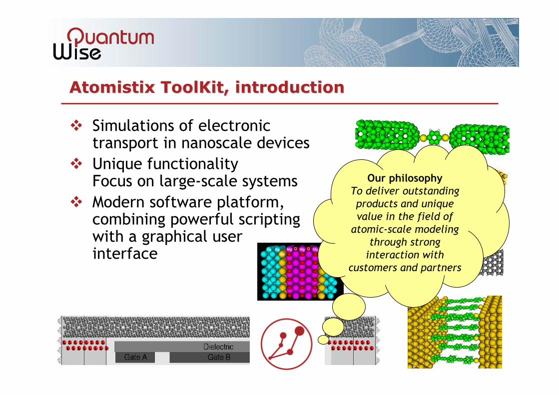
AtomistixAtomistix ToolKitToolKit, introduction, introduction
Simulations of electronic transport in nanoscale devices
Unique functionalityFocus on large-scale systems
Modern software platform, combining powerful scripting with a graphical user interface
Our philosophy
To deliver outstanding
products and unique
value in the field of
atomic-scale modeling
through strong
interaction with
customers and partners

Functionalized carbon nanotubes
Contact resistance and capacitance of metal-nanotube and nanotube-nanotube contacts; Schottkybarrier
Application areas (1/2)Application areas (1/2)
Graphene devices
Molecular junctions and tunneling devices (rectification, NDR)

Reaction paths on surfaces for catalysis
Application areas (2/2)Application areas (2/2)
Spin-dependent transport across crystalline magnetotunnel junctions
Leakage currents in MOS structuresHigh-k dielectrics, complex interfaces
Defect states in semiconductors, nanowires, nanotubes
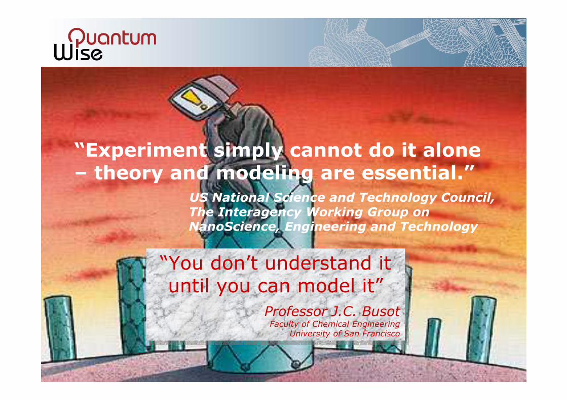
“Experiment simply cannot do it alone – theory and modeling are essential.”
US National Science and Technology Council, The Interagency Working Group on NanoScience, Engineering and Technology
“You don’t understand ituntil you can model it”
Professor J.C. BusotFaculty of Chemical Engineering
University of San Francisco
“You don’t understand ituntil you can model it”
Professor J.C. BusotFaculty of Chemical Engineering
University of San Francisco
OutlineOutline
Introduction
Complex boundary conditions
Examples
Details of the software

Reaching the quantum limitReaching the quantum limit
0
5
10
15
20
25
30
35
0 150
Length [nm]
Resis
tan
ce [
k Ω
]
Classical resistance
Quantumresistance
~50 nm

Current mechanismCurrent mechanism
Propagation of wave function
Ballistic, coherent transport
Calculation of transmission amplitudes t

Transport regimesTransport regimes

Essential points of atomistic device modelingEssential points of atomistic device modeling
Atomistic, quantum models
Accurate electronic structure» Tight-binding works – when it works…
» DFT most transferable, but heavy. Semiconductors?
» Semi-empirical methods
Describe voltage drop» Self-consistent response to electrostatic environment
Proper boundary conditions» Transport under finite bias -> NEGF
» Gates
Transmission spectrum usually bias-dependent » Non-linear response

Junctions Interfaces Surfaces
ComplexComplex boundaryboundary conditionsconditions
The main application areas in nanotechnologyare related to effects occurring at
It is critical to be able to
accurately model systems with
complex boundary conditions
from quantum theory
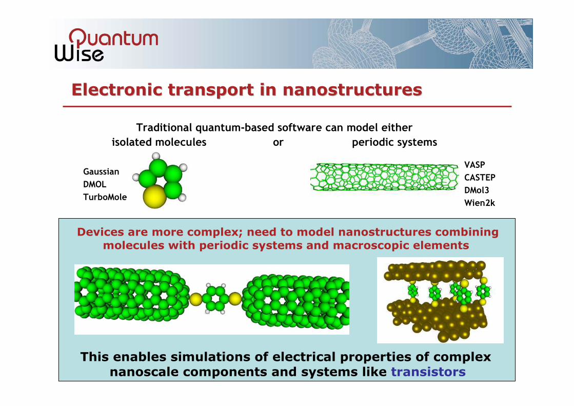
Traditional quantum-based software can model either
isolated molecules or periodic systems
Devices are more complex; need to model nanostructures combining
molecules with periodic systems and macroscopic elements
This enables simulations of electrical properties of complex
nanoscale components and systems like transistors
Gaussian
DMOL
TurboMole
VASP
CASTEP
DMol3
Wien2k
Electronic transport in Electronic transport in nanostructuresnanostructures
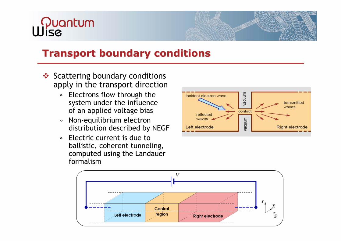
Transport boundary conditionsTransport boundary conditions
Scattering boundary conditions apply in the transport direction
» Electrons flow through the system under the influence of an applied voltage bias
» Non-equilibrium electron distribution described by NEGF
» Electric current is due to ballistic, coherent tunneling, computed using the Landauerformalism

• Density-functional theory or extended Hückel• LCAO, numerical orbitals with finite range• DFT uses norm-conserving pseudopotentials• Extended Hückel has Hartree term for SCF
Electronic structure
Transport• Exact description of semi-infinite electrodes using self-energies• Non-equilibrium electron distribution using NEGF• Calculation of electron current by Landauer formalism
HH DD
Bulk
region
Bulk
region
TwoTwo--probe methodologyprobe methodology
M. Brandbyge, J.-L. Mozos, P. Ordejón, J. Taylor, K. Stokbro, Physical Review B 65, 165401 (2002)
-------------------Interaction region------------------

DFT modelDFT model
SIESTA method» Own implementation
Linear combination of numerical atomic orbitals (LCAO)
Finite range» Sparse matrices (+)
» Non-variational (−) Norm-conserving Troullier-Martins
pseudopotentials
LDA/GGA
J. M. Soler, E. Artacho, J. D. Gale, A. García, J. Junquera, P. Ordejón, and D. Sánchez-Portal, J. Phys. Condens. Matter 14, 2745 (2002)
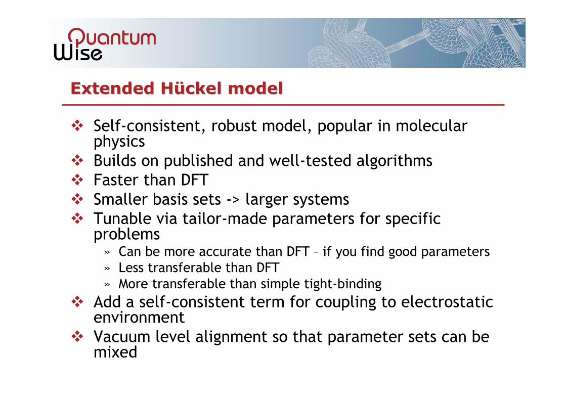
Extended Extended HHüückelckel modelmodel
Self-consistent, robust model, popular in molecular physics
Builds on published and well-tested algorithms
Faster than DFT
Smaller basis sets -> larger systems
Tunable via tailor-made parameters for specific problems» Can be more accurate than DFT – if you find good parameters
» Less transferable than DFT
» More transferable than simple tight-binding
Add a self-consistent term for coupling to electrostaticenvironment
Vacuum level alignment so that parameter sets can be mixed

ExtendedExtended HHüückelckel theorytheory (EHT)(EHT)
[ ] )ˆ()2()2()!2(
)( 21 1222
1211
1
rYeCeCn
rr lm
rnrnln
nlmηη ηηφ −+−+
−−
+=rSlater type
LCAO orbital
∫= drrrS jiij )()(rr φφOverlap
matrix
≠+
==
jiS
jiH
ijji
i
ij )(2
1 εεβ
εHamiltonian
M. Wolfsberg, and L. Helmholtz. J. Chem. Phys. 20, 837 (1952)
J. H. Ammeter et. al., J. Am. Chem. Soc. 100, 3686 (1978)
M. H. Whangbo, and R. Hoffmann. J. Chem. Phys. 68, 5498 (1978)

CurrentlyCurrently 300 parameters in ATK300 parameters in ATK--SESE
YAEMOP (Yet Another Extended Huckel Molecular Orbital Program)Hoffmann + Muller parameters
> Fitted to molecules
> Full periodic system
> High transferability
Jorge Cerda’s homepage> Special parameters fitted to particular systems
M. Wolfsberg, and L. Helmholtz. J. Chem. Phys. 20, 837 (1952)
J. H. Ammeter et. al., J. Am. Chem. Soc. 100, 3686 (1978)M. H. Whangbo, and R. Hoffmann. J. Chem. Phys. 68, 5498 (1978)
J. Cerda and F. Soria, Phys. Rev. B 61, 7965 (2000)

Band Band structurestructure of of siliconsilicon, , comparisoncomparison
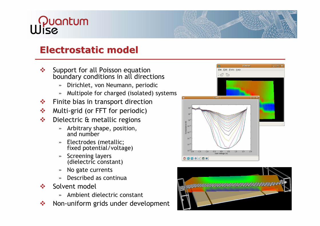
Electrostatic modelElectrostatic model
Support for all Poisson equation boundary conditions in all directions
» Dirichlet, von Neumann, periodic
» Multipole for charged (isolated) systems
Finite bias in transport direction
Multi-grid (or FFT for periodic)
Dielectric & metallic regions
» Arbitrary shape, position, and number
» Electrodes (metallic; fixed potential/voltage)
» Screening layers (dielectric constant)
» No gate currents
» Described as continua
Solvent model
» Ambient dielectric constant
Non-uniform grids under development

Virtual experimentsVirtual experiments
Current–voltage characteristics» NDR, rectification, switching, etc
» Conductance
» Tunnel magneto-resistance
» Spin current
» Schottky barrier
» Contact resistance
Transistor characteristics (gates)
Voltage drop
Thermionic emission
Co-linear spin torque transfer
Bias-induced forces
Basic electronic structure» Band structure
» DOS
» Molecular spectra
» Total energies
Reaction pathway & activation energy

TwoTwo--probe systems, electrodesprobe systems, electrodes
A two-probe system consists of» left and right electrodes
» a central scattering region
Each electrode is a semi-infinite periodic system» Cleaved bulk crystal (eg. a gold
[111] surface)
» Carbon nanotube, graphene, atomic chain, etc
The two electrodes can be different» Two different metals
» Two different carbon nanotubes
» Metal–nanotube contact
» Different spin-polarization (magnetic tunnel junctions)
Mg OCo
Si
Mn
Parallel or Anti-Parallel

Scattering regionScattering region
The scattering region can be ... anything!» A molecule (e.g. between two metal surfaces)
» A piece of a carbon nanotube (e.g. a metal–nanotube–metal contact)
» A graphene nanoribbonzigzag/armchair contact
» A periodic structure (layered interfaces)
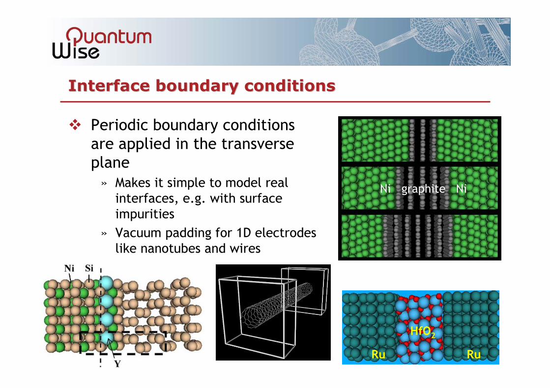
Interface boundary conditionsInterface boundary conditions
Periodic boundary conditions
are applied in the transverse
plane
» Makes it simple to model real
interfaces, e.g. with surface
impurities
» Vacuum padding for 1D electrodes
like nanotubes and wires
HfO2
Ru Ru
Ni graphite Ni

AnalyzingAnalyzing quantumquantum transport transport mechanismsmechanisms
ATK provides several analysis tools for
understanding transport mechanisms» Transmission spectrum and surface DOS/PDOS
» K-point resolved transmission
» Molecular projected self-consistent Hamiltonian
(MPSH) eigenvalues and eigenstates
» Transmission eigenvalues and eigenchannels

LargeLarge--scalescale systemssystems
Nanowires, multiwall nanotubes and complex interface structures can easily contain several hundred atoms per unit cell
In order to treat effects from defects (including doping), very large unit cells are also required
Need to treat thousands of atoms
Si fcc
O

Ways Ways towardstowards largerlarger systemssystems
Method
» Numerical orbitals allow larger systems than plane waves
» Less sophistication (doesn’t always mean lower accuracy!)
Multi-scale
» Coupling to continuum models
» Extract effective parameters for higher-level models
Parallelization
» In particular memory

Finite element Macro scale
Empirical potentialsForce fields, glue potentials, …
Semi-empiricalTight-binding, Hückel, AM1, PM3, …
DFTOrbitals, plane waves
Level of sophistication
Number of atoms in the system under consideration
101 103102 104 105 107106
SCFH-F
Correlations: CC, CI, MP perturbation theory, GW
Correlations: LDA, GGA, etc

FEM FEM gridsgrids
3D grids present memory bottle-necks for large systems
Lots of vacuum for nanotubes& graphene means regular grids are inefficient and wasteful
Reduce memory & increase performance by using FEM grids
Point density derived from charge density
Ongoing project with Copenhagen University
OutlineOutline
Introduction
Complex boundary conditions
Examples
Details of the software

OhmicOhmic contacts on siliconcontacts on silicon--carbidecarbide
SiC / Ti3SiC2 interface
Experimental result: ohmic contacts on SiCformed as epitaxial, coherent and atomically ordered interface
Modeling provides quantitative predicts that the interface can trap a layer of C and lower the Schottkybarrier
Wang et al.,
PRB 80, 245303 (2009)
Adv. Mat. 21, 4966 (2009)
Si/Si
Si/C/Si

Resistive switchResistive switch
Cu/Ta2O5/Pt heterojunction
Comparison of β vs δ phase of Ta2O5
No conducting channel formed from Cu to Pt through δ-Ta2O5 = “off” state
Gu et al., J. Appl. Phys.
106, 103713 (2009)
CB formed by Ta d-states
VB formed by O p-states

PtPt––SrTiO3SrTiO3––Pt Pt heterostructuresheterostructures
Intrinsically closed conductance channel in SrTiO3 opens up after doping substitutional atoms of higher valency
Enhancement in electron transmission at Fermi level, drastic increase in the current with bias
Z. Wang et. al., APL 94,
252103 (2009)
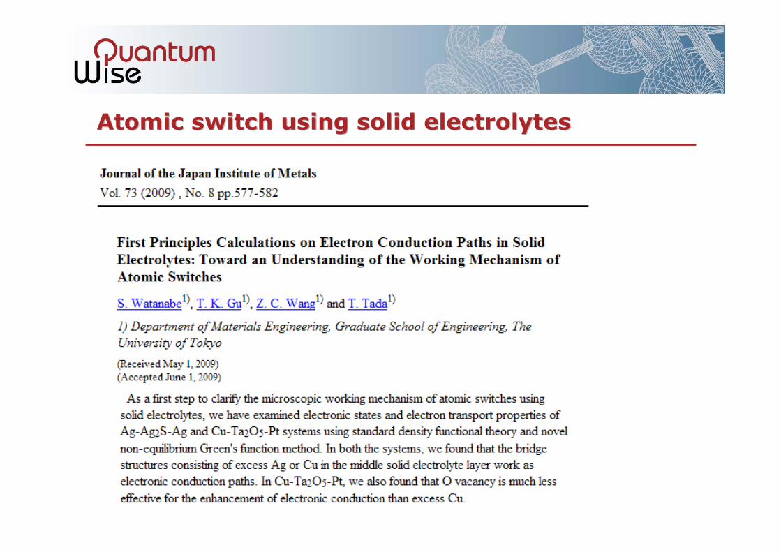
Atomic switch using solid electrolytesAtomic switch using solid electrolytes
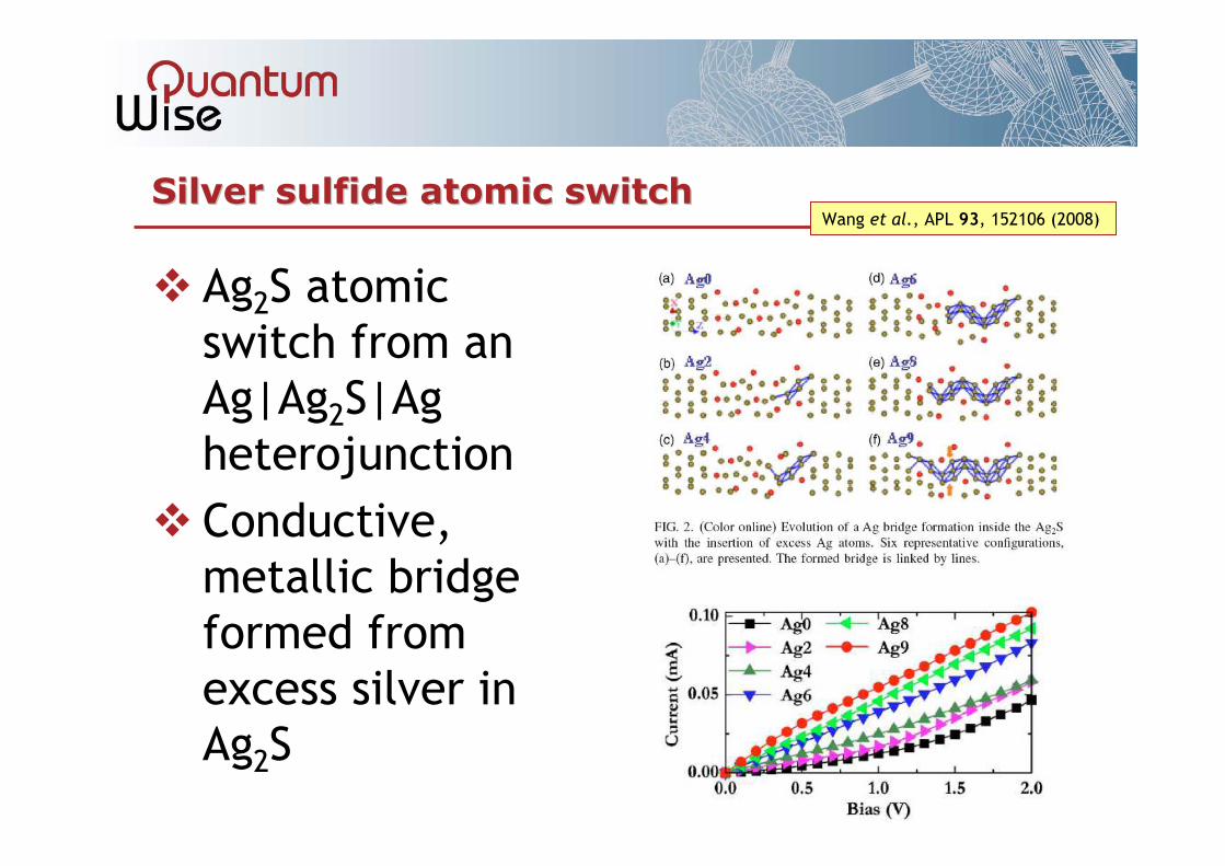
Silver sulfide atomic switchSilver sulfide atomic switch
Ag2S atomic
switch from an
Ag|Ag2S|Ag
heterojunction
Conductive,
metallic bridge
formed from
excess silver in
Ag2S
Wang et al., APL 93, 152106 (2008)
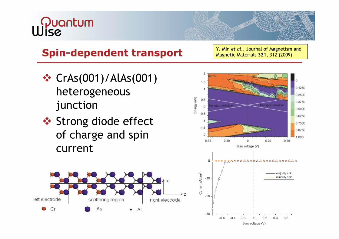
SpinSpin--dependent transportdependent transport
CrAs(001)/AlAs(001)
heterogeneous
junction
Strong diode effect
of charge and spin
current
Y. Min et al., Journal of Magnetism and
Magnetic Materials 321, 312 (2009)

ShapesShapes of of graphenegraphene
Resonant-tunneling double-barrier diode (RTDB)
Commensurate graphene or graphene/B-N armchairstructures
T-shaped junctions
Current depends strongly on stem height
Conductivity controllable by selective doping
Sevincli et al.,
PRB 78, 245402
(2008)
OuYang et al.,
Nanotechnology 20,
055202 (2009)

Gas Gas sensingsensing
Amino acids by CNTs
NO2 by SiC nanotubes
By graphene (CO, NO, NO2, NH3)
Defect/doped vs. pristine
Abadir et al.,
Int. J. High Speed Electr. Syst., 18, 879 (2008)
8th IEEE Conf. Nanotech., 230 (2008)
Ruixhue et al., J. Semicond. 30, 114010 (2009)
Zhang et al.,
Nanotechnology
20, 185504 (2009)
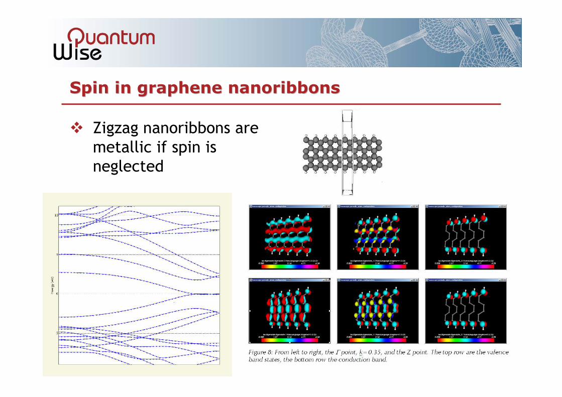
Spin in Spin in graphenegraphene nanoribbonsnanoribbons
Zigzag nanoribbons are
metallic if spin is
neglected

SpintronicsSpintronics in in graphenegraphene
Anti-ferromagnetic spin configuration
Spin opens up a band gap
Spin states localize on opposite
sides of the ribbon
Majority/minority still fully
degenerate
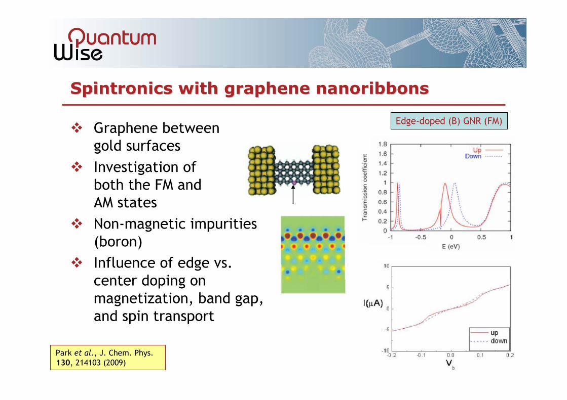
Graphene between
gold surfaces
Investigation of
both the FM and
AM states
Non-magnetic impurities
(boron)
Influence of edge vs.
center doping on
magnetization, band gap,
and spin transport
SpintronicsSpintronics with with graphenegraphene nanoribbonsnanoribbons
Park et al., J. Chem. Phys.
130, 214103 (2009)
Edge-doped (B) GNR (FM)
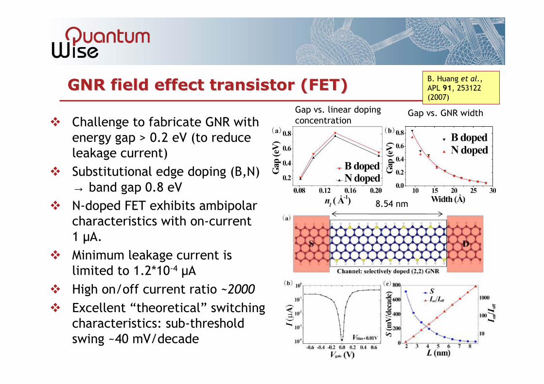
GNR field effect transistor (FET)GNR field effect transistor (FET)
Challenge to fabricate GNR with
energy gap > 0.2 eV (to reduce
leakage current)
Substitutional edge doping (B,N)
→ band gap 0.8 eV
N-doped FET exhibits ambipolar
characteristics with on-current
1 µA.
Minimum leakage current is
limited to 1.2*10-4 µA
High on/off current ratio ~2000
Excellent “theoretical” switching
characteristics: sub-threshold
swing ~40 mV/decade
B. Huang et al.,
APL 91, 253122 (2007)
Gap vs. linear doping
concentrationGap vs. GNR width
8.54 nm
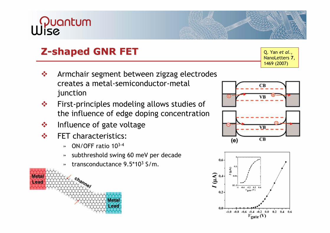
ZZ--shaped GNR FETshaped GNR FET
Armchair segment between zigzag electrodes
creates a metal-semiconductor-metal
junction
First-principles modeling allows studies of
the influence of edge doping concentration
Influence of gate voltage
FET characteristics:
» ON/OFF ratio 103-4
» subthreshold swing 60 meV per decade
» transconductance 9.5*103 S/m.
Q. Yan et al.,
NanoLetters 7,
1469 (2007)
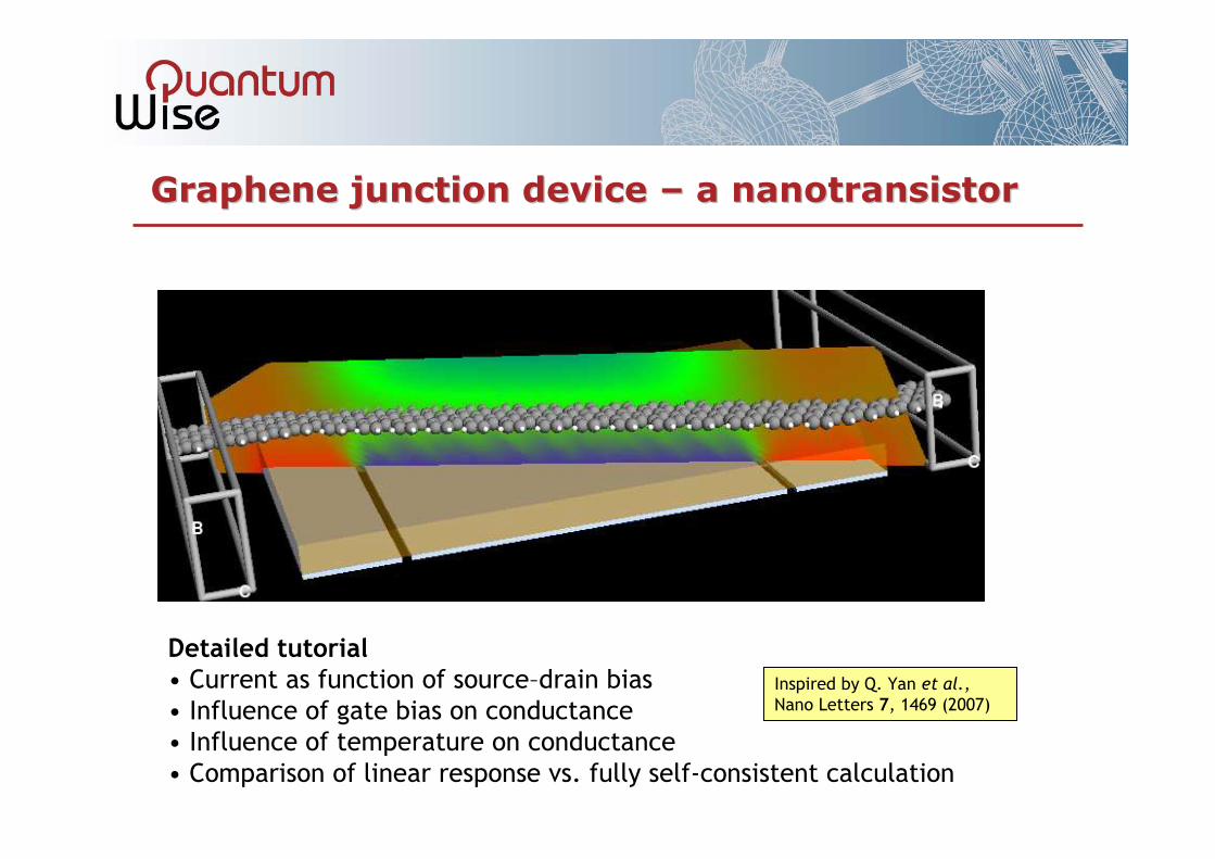
Graphene junction device Graphene junction device –– a a nanotransistornanotransistor
Detailed tutorial
• Current as function of source–drain bias
• Influence of gate bias on conductance
• Influence of temperature on conductance
• Comparison of linear response vs. fully self-consistent calculation
Inspired by Q. Yan et al.,
Nano Letters 7, 1469 (2007)
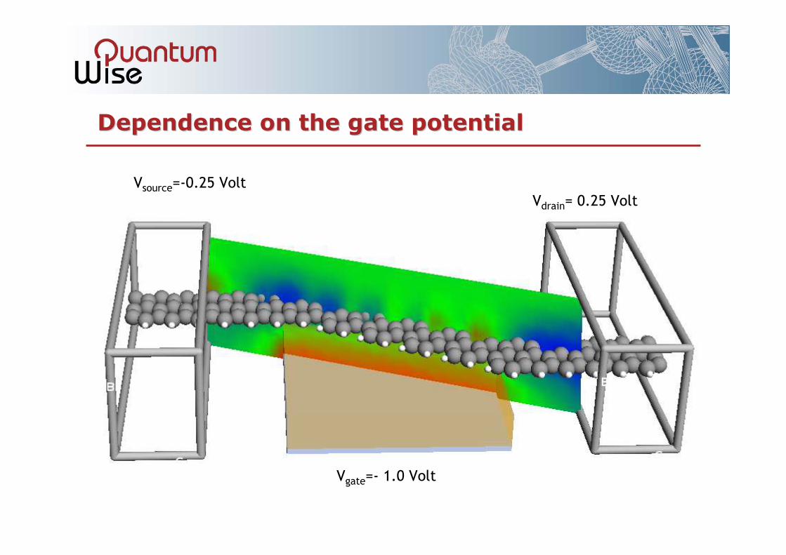
DependenceDependence onon the gate potentialthe gate potential
Vsource=-0.25 Volt
Vgate=- 1.0 Volt
Vdrain= 0.25 Volt
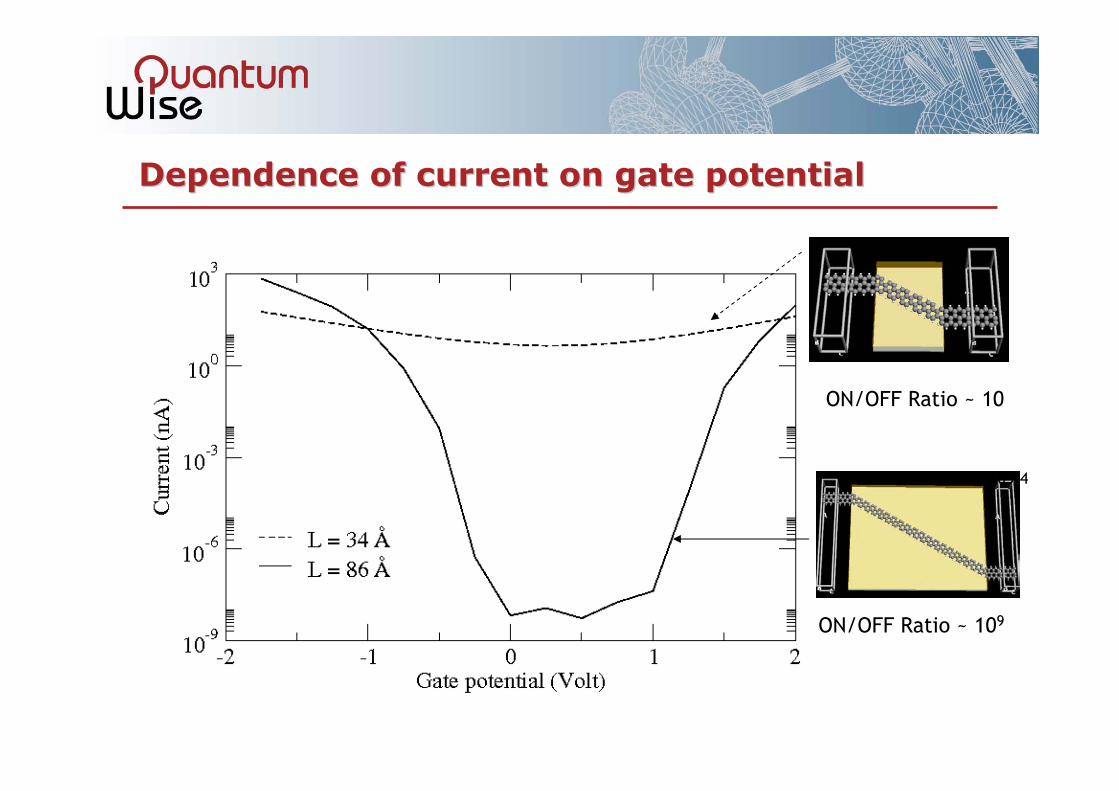
DependenceDependence of of currentcurrent onon gate potentialgate potential
ON/OFF ratio 103-4
ON/OFF Ratio ~ 10
ON/OFF Ratio ~ 109
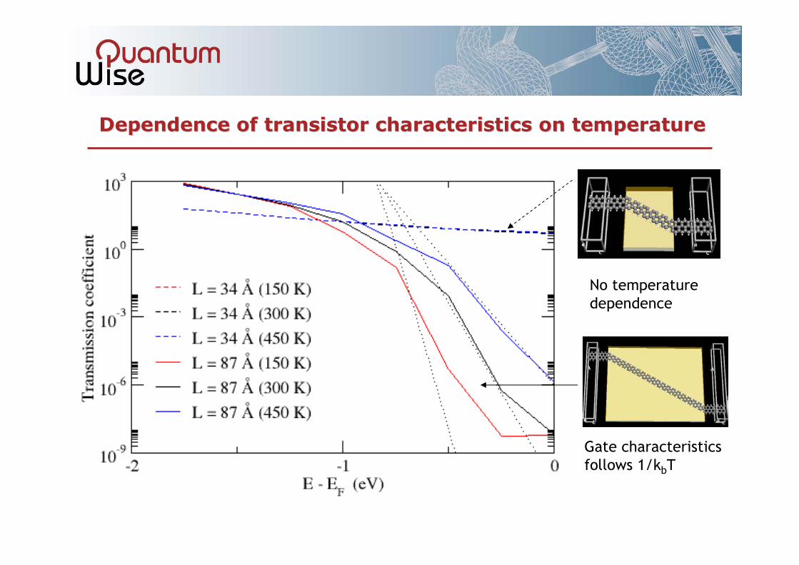
DependenceDependence of transistor of transistor characteristicscharacteristics onon temperaturetemperature
No temperature
dependence
Gate characteristics
follows 1/kbT
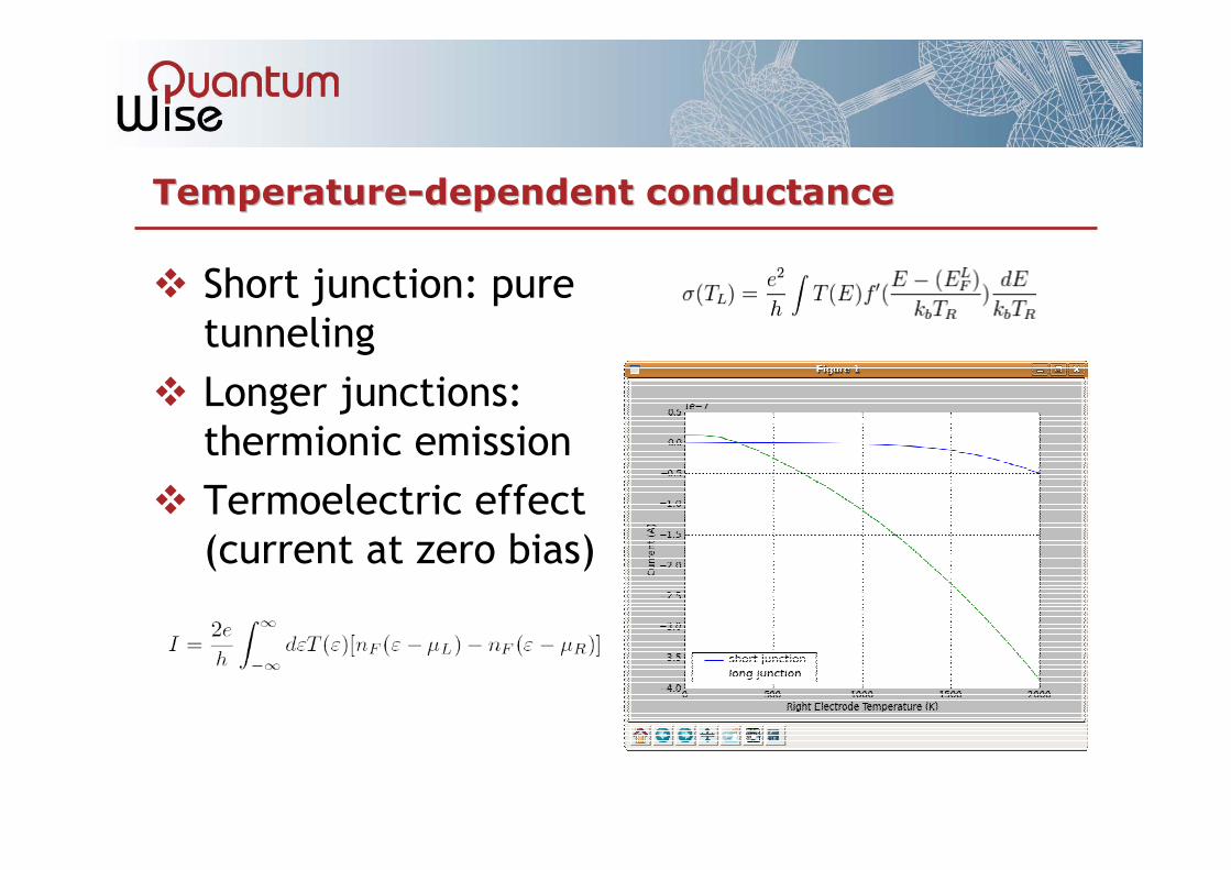
TemperatureTemperature--dependentdependent conductanceconductance
Short junction: pure
tunneling
Longer junctions:
thermionic emission
Termoelectric effect
(current at zero bias)

Nanoelectromechanical
force/displacement
sensor
On/off:103 @ 20 mV bias
and 5.6 V switching gate
bias
BilayerBilayer structuresstructures
Armchair bilayer ribbon
Gap vs. interlayer
separation
Edge doping
Lam & Liang, APL
92, 223106 (2008)
Lam et al., APL 95,
143107 (2009)

CNT/GNR junctionsCNT/GNR junctions
Li et al.,
Nanotechnology 20,
225202 (2009)
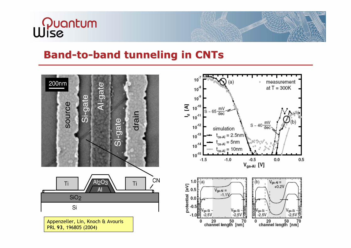
BandBand--toto--band tunneling in band tunneling in CNTsCNTs
Appenzeller, Lin, Knoch & Avouris
PRL 93, 196805 (2004)
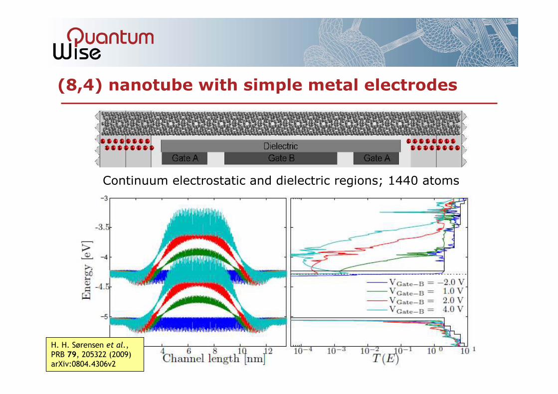
(8,4) nanotube with simple metal electrodes
Continuum electrostatic and dielectric regions; 1440 atoms
H. H. Sørensen et al.,
PRB 79, 205322 (2009)
arXiv:0804.4306v2
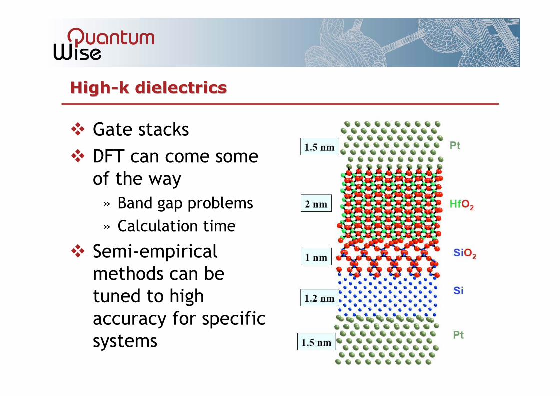
HighHigh--k dielectricsk dielectrics
Gate stacks
DFT can come some
of the way
» Band gap problems
» Calculation time
Semi-empirical
methods can be
tuned to high
accuracy for specific
systems

Grain boundary simulationGrain boundary simulation
Single grain boundary (GB) reflectivity in Cu and Ag
Twin/non-twin GB
Vacancies, disorder, orientation
Results consistent with experiments
May point to limitations in the Mayadas-Shatzkes model (one-parameter reflectivity averaged over all GBs)
Feldman et al.,
arXiv:0908.2252
SBH modificationSBH modification
Fermi level unpinning and Schottky barrier modification by incorporation of Ti, C, V, Y in NiSi2/Si interfaces
Interface states in gap region are greatly decreased when Si dangling bonds are saturated
Gives new pinning-free interfacial structure
Li Geng et al.,
Chinese Physics Letters 26, 037306 (2009) IEEE EDL 29, 746 (2008)
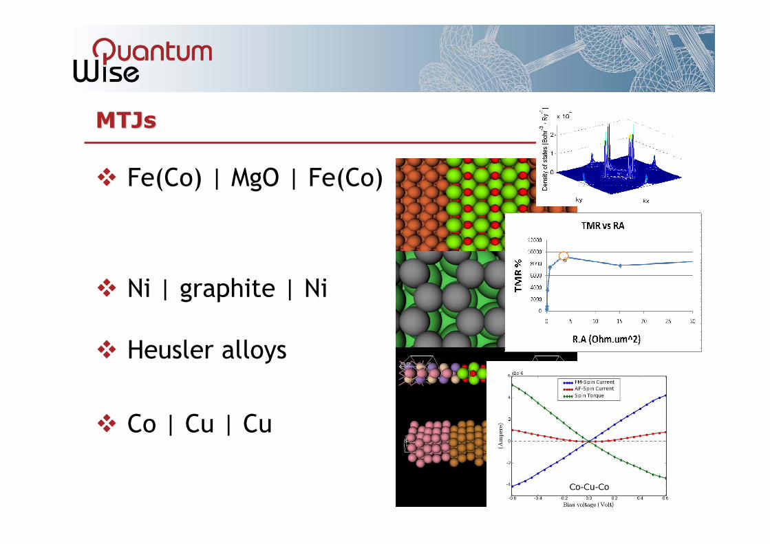
MTJsMTJs
Fe(Co) | MgO | Fe(Co)
Ni | graphite | Ni
Heusler alloys
Co | Cu | Cu

Coulomb Coulomb blockadeblockade transport regimetransport regime
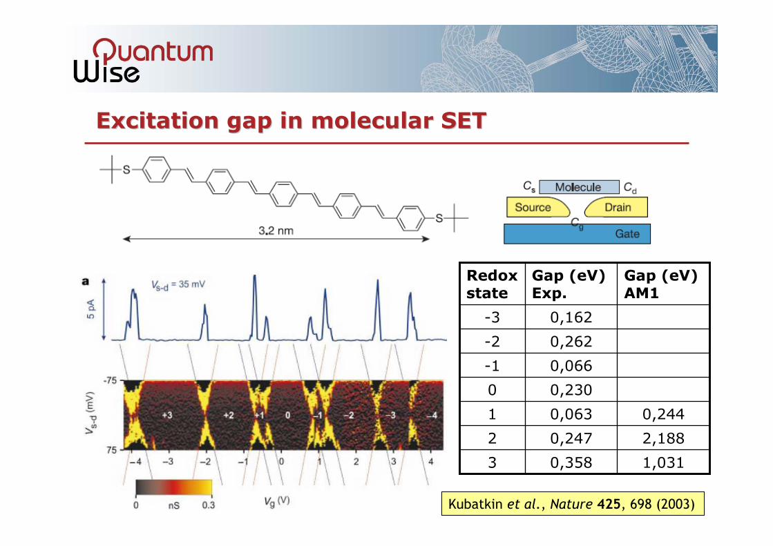
Excitation gap in molecular SETExcitation gap in molecular SET
0,2440,0631
2,1880,2472
1,0310,3583
0,2300
0,066-1
0,262-2
0,162-3
Gap (eV) AM1
Gap (eV) Exp.
Redoxstate
Kubatkin et al., Nature 425, 698 (2003)

ChargingCharging energyenergy in a SET in a SET environmentenvironment
0.72−5.90
Vacuum, neutral
8.392.35
−9.16−15.73
Vacuum, charged
(>1.29)−9.25
Exp
−0.111.33
−7.97−9.43
SET
−1 0
+1 +2
State
BenzeneBenzene
Charged molecule in the gas
phase using multi-pole
boundary conditions
Energies in eV

Charge Charge stabilitystability diagramdiagram
Energy of different charge states
0
1
2
-1
-2

OutlineOutline
Introduction
Complex boundary conditions
Examples
Details of the software

Graphical
User InterfaceUser Scripts
Proprietary Engines
• Atomic-scale modeling of electronic devices using DFT or semi-empirical methods
• Massively parallel software
• Fast relaxations
• Integration with continuum modeling
Python Interface
API Modules
Python Wrappers
Open-Source / 3rd-Party Software
GPAW, Dacapo
AbInit, VASP
Socorro
Atomistix ToolKit (ATK)Atomistix ToolKit (ATK)

Fully programmable object-oriented scripting interface to ATK
» Transparent – the Python syntax is simple yet powerful, with good structural overview
» Modularized
» Extendible – integrate your own or third-party algorithms with ATK
Tying the platform together
» Integrated in the GUI (see later)
» Wrapping of third-party codes
Interpreted language
» Can be used interactively
» Comes with “batteries included”(scientific modules)
» Performance disadvantage (solvable, all performance critical parts are written in C++, Fortran, or use external optimized libraries)
» Cross-platform compatible source code
ATK PythonATK Python
© Frank Stajano


Scripting interface benefitsScripting interface benefits
Control of parameters
» Loop over physical parameters
» Set up parametrized geometries
» Detailed control of basis set
Control of flow
» Converge w.r.t. accuracy parameters
» Decision-making scripts
Access to raw data
» Customized analysis (integrate over spatial coordinates, subtract grids, …)
» Export data in any desired format
Extendibility
» Customized modules (3rd party/in-house/from QuantumWise to customer)
» Implement new algorithms
» Wrap other software packages
» Anything you otherwise can do in Python, applied to quantum chemistry and electronic transport!

Graphical user interface (GUI)Graphical user interface (GUI)
Guide the user through the work-flow
» Set up the device structure
» Optimize the geometry
» Define the quantum-chemical environment (method & parameters)
» Run the calculations
» Analyze & plot the results (in 2D and 3D)
Interactive generation and export of scripts + internal script interpreter
» Helps the user learn the command-line interface
» Facilitates use of external computational resources
» Assists the user during prototyping of scripts
Plug-ins (both on scripting and GUI level)
» User can expand the functionality of the interface
» Both geometry setup and analysis modules available
» Deliver customized functionality to individual users, or via Forum etc
Cross-platform compatible input and output filesHfO2
Ru Ru

GUI (Virtual GUI (Virtual NanoLabNanoLab))

Performance Performance examplesexamples
State-of-the-art parallel DFT code
» MPI parallelization for k-points and energy points
» OpenMP for threading on multi-core CPUs
» Optimized code & libraries provideexcellent performance and scaling
Examples:
» MgO bulk supercell with 1,024 atoms converges in 16 hours on a single node, using 3 Gb memory (DZP basis set)
» Au/Si/Au two-probe with 1,166 atoms, 24 hours on 10 nodes, 2 Gb (SZ basis set)

Supercluster Supercluster parallelparallel scalingscaling & & speedupspeedup
Model: Au-Si nanowire-Au
CPU cores
Speedup
Total calculation time
0
20
40
60
80
100
120
140
160
4 8 16 32 64 128
CPU Cores
Cal
cula
tion
time
(hou
rs)
ATK 2008.02
ATK 2008.10
ATK 2008.10

SummarySummary
Modeling to complement experiments
Complex boundary conditions
Large systems, multi-scale approaches
Accurate electronic structure
Response to electrostatic environment
Modern, user-friendly & flexible software
platform

Thank youThank youfor your attention!for your attention!
To learn more To learn more –– please stick around!please stick around!
And/or visitAnd/or visit
quantumwise.comquantumwise.com
to request a to request a freefree trial licensetrial license