attacking atmel's cryptomemory eeprom with special-purpose
TRANSCRIPT
Attacking Atmel’s CryptoMemory EEPROMwith Special-Purpose Hardware
Alexander Wild, Tim Guneysu, and Amir Moradi
Horst Gortz Institute for IT Security, Ruhr University Bochum, Germany{alexander.wild, tim.gueneysu, amir.moradi}@rub.de
Abstract. Atmel’s CryptoMemory devices are non-volatile memorieswith cryptographically secured access control. Recently, the authentica-tion mechanism of these devices have been shown to be severely vulnera-ble. More precisely, to recover the secret key the published attack requiresonly two to six days of computation on a cluster involving 200 CPU cores.In this work, we identified and applied theoretical improvements to thisattack and mapped it to a reconfigurable computing cluster, known asRIVYERA. Our solution provides significantly higher performance ex-ceeding the previous implementation by a factor of 7.27, revealing thesecret key obtained from the internal state in 0.55 days on average usingonly 30 authentication frames.
1 Introduction
In 2002 Atmel introduced a secure memory device with authentication calledCryptoMemory [2,13] which is basically an Electrically Erasable ProgrammableRead-Only Memory (EEPROM) augmented with a secure access control unit.
Due to the low cost and simplicity of deployment the device is employed in awide range of commercial products, e.g., as key storage of the HDCP system inNVIDIA’s graphic cards [16], Labgear’s digital satellite receivers [15], Microsoft’sZune Player [7] and SanDisk’s Sansa Connect [9] using the CryptoMemory aspart of their DRM system implementation. Further examples of CryptoMemorydeployment are printer and printer cartridge manufacturers like Dell, Ricoh,Xerox, and Samsung [14]. Furthermore, Atmel’s CryptoMemory is placed inauthentication tokens from Digitrade [6] and Datakey Electronics [1].
The specification of the Atmel cipher was kept secret till ACM CCS 2010where Garcia et al. presented their findings obtained from reverse engineer-ing [8]. They also showed significant weaknesses by analyzing the authenticationprotocol. One year later Biryukov et al. published a more efficient method which– with a probability of 50% – is capable of extracting the secret key from 30authentication recordings [4]. This attack runs on a computing cluster with 200Central Processing Unit (CPU) cores and needs two to six days to recover the se-cret. Another attack based on power side-channels has also been reported in [3].This attack lasting a few minutes, however, needs physical access to the deviceand a special side-channel measurement setup to extract the secret key fromabout 100 power traces.
2
Our contribution: In this work, we improve and map the best known crypt-analytic attack on CryptoMemory devices published in [4] to special-purposehardware, namely the RIVYERA S3-5000 reconfigurable computing cluster [17].Our improvement of the cryptanalytic setup in addition to our hardware-basedimplementation leads to a speedup factor of 7.27 compared to the previously re-ported results. In short, our implementation is able to extract the internal stateof the cipher from 30 authentication frames within 0.55 days on average whichimpressively demonstrates that none of the products mentioned above can beconsidered as secure. Given a cluster such as RIVYERA, our attack configura-tion is also a power-efficient solution. For a run with 30 frames, the hardwarecluster consumes 8.6KWh instead of 245.76KWh the CPU cluster per attackeddevice.
Outline: In Section 2 we provide preliminary information on CryptoMemory,previously published attacks and RIVYERA. Improvements of the attack arepresented in Section 3. Section 4 and 5 deals with our implementation archi-tectures before we compare our results in Section 6 with those of a CPU-basedimplementation. Finally, our conclusions are given by Section 7.
2 Background
In this section we briefly restate the required background of our work. Thesection includes specification of the targeted cipher, the underlying protocol, theattack of [4], and our computing cluster.
2.1 CryptoMemory Stream Cipher
The cipher state consists of four shift registers - the left, middle, right andfeedback register.
Definition 1. The state S = (l,m, r, f) is an element of F1172 and consists of:
Left Register: l = (l0, l1 . . . , l6) ∈ (F52)7
Middle Register: m = (m0,m1 . . . ,m6) ∈ (F72)7
Right Register: r = (r0, r1 . . . , r4) ∈ (F52)5
Feedback Register: f = (f0, f1) ∈ (F42)2
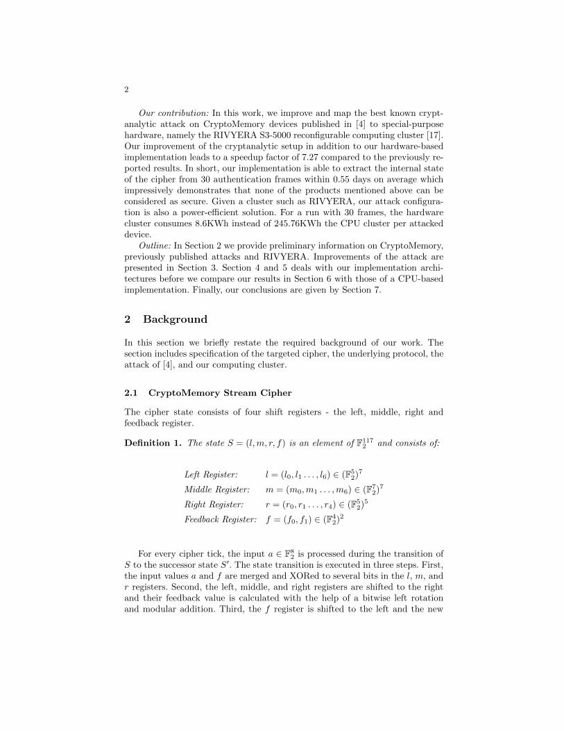
For every cipher tick, the input a ∈ F82 is processed during the transition of
S to the successor state S′. The state transition is executed in three steps. First,the input values a and f are merged and XORed to several bits in the l, m, andr registers. Second, the left, middle, and right registers are shifted to the rightand their feedback value is calculated with the help of a bitwise left rotationand modular addition. Third, the f register is shifted to the left and the new
3
calculated cipher output nibble becomes the new first element of f . Figure 1provides an overview of the cipher operation. The core operations of the cipherare given by the following definitions:
Definition 2. The bitwise left rotation operator L : Fn2 → Fn
2 is defined by:
L(x0x1 . . . xn−1) = (x1 . . . xn−1x0)
.
Definition 3. Let ⊕ be a bitwise XOR operator Fn2 × Fn
2 → Fn2 .
Definition 4. The modular addition operator � : Fn2 × Fn
2 → Fn2 is defined as:
x� y =
{x+ y( mod 2n − 1) if x = y = 0 or x+ y 6= 0 ( mod 2n − 1)
2n − 1 otherwise
Definition 5. Let a and b be defined as: a ∈ F82 and b = a⊕ f0f1. Further, the
successor state S′ = (l′,m′, r′, f ′) is defined as follows:
l′0 := l3 � L(l6), l′3 := l2 ⊕ b3b4b5b6b7, l′i+1 := li i ∈ {0, 1, 3, 4, 5}m′0 := m5 � L(m6), m′5 := m4 ⊕ b4b5b6b7b0b1b2, m′j+1 := mj j ∈ {0, 1, 2, 3, 5}r′0 := r2 � r4, r′2 := r1 ⊕ b0b1b2b3b4, r′k+1 := rk k ∈ {0, 2, 3}f ′0 := f1, f ′1 := output(S′)
0 1 2 3 4 5 6 0 1 2 3 4 5 6 0 1 2 3 4 0 1
l m r
ab
10
lk rkmk
b3b4b5b6b7 b4b5b6b7b0b1b2 b0b1b2b3b4
4 4
4
7 55
4
8
f
Fig. 1. The CryptoMemory keystream generator [4].
Definition 6. The cipher output function is defined as follows while i is a bit-selector:
output(S′)i =
{lki = (l′0 ⊕ l′4)i+1, if m′0,i+3 = 0
rki = (r′0 ⊕ r′3)i+1, if m′0,i+3 = 1 i ∈ {0, . . . , 3}
4
Definition 7. Let suc be the state transition function with input a, S and out-put S′ = suc(a, S). Further, sucn(a, S) is defined as multiple application of suctransforming S into its n-th successor state.
suc1(a, S) := suc(a, S)
sucn(a, S) := sucn−1(a, suc(a, S)) for n > 1
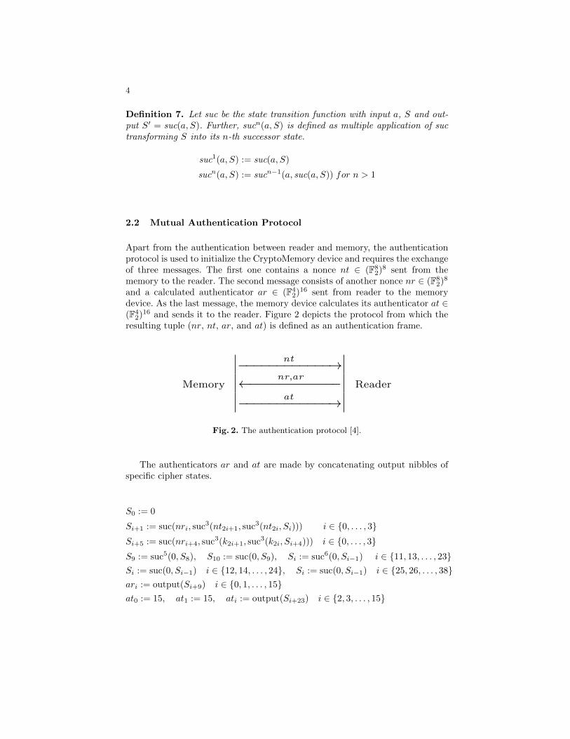
2.2 Mutual Authentication Protocol
Apart from the authentication between reader and memory, the authenticationprotocol is used to initialize the CryptoMemory device and requires the exchangeof three messages. The first one contains a nonce nt ∈ (F8
2)8 sent from thememory to the reader. The second message consists of another nonce nr ∈ (F8
2)8
and a calculated authenticator ar ∈ (F42)16 sent from reader to the memory
device. As the last message, the memory device calculates its authenticator at ∈(F4
2)16 and sends it to the reader. Figure 2 depicts the protocol from which theresulting tuple (nr, nt, ar, and at) is defined as an authentication frame.
nt−−−−−−−−−−−−→Memory
nr,ar←−−−−−−−−−−−− Readerat−−−−−−−−−−−−→
Fig. 2. The authentication protocol [4].
The authenticators ar and at are made by concatenating output nibbles ofspecific cipher states.
S0 := 0
Si+1 := suc(nri, suc3(nt2i+1, suc3(nt2i, Si))) i ∈ {0, . . . , 3}Si+5 := suc(nri+4, suc3(k2i+1, suc3(k2i, Si+4))) i ∈ {0, . . . , 3}S9 := suc5(0, S8), S10 := suc(0, S9), Si := suc6(0, Si−1) i ∈ {11, 13, . . . , 23}Si := suc(0, Si−1) i ∈ {12, 14, . . . , 24}, Si := suc(0, Si−1) i ∈ {25, 26, . . . , 38}ari := output(Si+9) i ∈ {0, 1, . . . , 15}at0 := 15, at1 := 15, ati := output(Si+23) i ∈ {2, 3, . . . , 15}
5
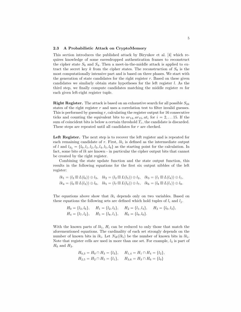
2.3 A Probabilistic Attack on CryptoMemory
This section introduces the published attack by Biryukov et al. [4] which re-quires knowledge of some eavesdropped authentication frames to reconstructthe cipher state S8 and S4. Then a meet-in-the-middle attack is applied to ex-tract the secret key k from the cipher states. The reconstruction of S8 is themost computationally intensive part and is based on three phases. We start withthe generation of state candidates for the right register r. Based on these givencandidates we similarly obtain state hypotheses for the left register l. As thethird step, we finally compute candidates matching the middle register m foreach given left-right register tuple.
Right Register. The attack is based on an exhaustive search for all possible S24
states of the right register r and uses a correlation test to filter invalid guesses.This is performed by guessing r, calculating the register output for 16 consecutiveticks and counting the equivalent bits to ar14, ar15, ati for i = 2, . . . 15. If thesum of coincident bits is below a certain threshold Tr, the candidate is discarded.These steps are repeated until all candidates for r are checked.
Left Register. The next step is to recover the left register and is repeated foreach remaining candidate of r. First, lki is defined as the intermediate outputof l and lS0
= {l0, l1, l2, l3, l4, l5, l6} as the starting point for the calculation. Infact, some bits of lk are known - in particular the cipher output bits that cannotbe created by the right register.
Combining the state update function and the state output function, thisresults in the following equations for the first six output nibbles of the leftregister:
lk1 = (l3 � L(l6))⊕ l3, lk2 = (l2 � L(l5))⊕ l2, lk3 = (l1 � L(l4))⊕ l1,lk4 = (l0 � L(l3))⊕ l0, lk5 = (l7 � L(l2))⊕ l7, lk6 = (l8 � L(l1))⊕ l8.
The equations above show that lki depends only on two variables. Based onthese equations the following sets are defined which hold tuples of li and lj .
H0 = {l3, l6}, H1 = {l2, l5}, H2 = {l1, l4}, H3 = {l0, l3},H4 = {l7, l2}, H5 = {l8, l1}, H6 = {l9, l0}.
With the known parts of lki, Hi can be reduced to only those that match theaforementioned equations. The cardinality of each set strongly depends on thenumber of known bits in lki. Let NH(lki) be the number of known bits in lki.Note that register cells are used in more than one set. For example, l3 is part ofH0 and H3.
H0,3 = H0 ∩H3 = {l3}, H1,4 = H1 ∩H4 = {l2},H2,5 = H2 ∩H5 = {l1}, H3,6 = H3 ∩H6 = {l0}

6
Hi and Hi+3 can be further reduced by keeping only tuples that consist inl3−i and create the intersection set Hi,i+3. Additionally, H0, H3, and H6 arecombined toH0,3,6 = {l0, l3, l6} to do a similar reduction by keeping only possibleintersection values.
A yet unresolved problem is to choose a good starting point S0 to maximizethe reduction effect. A solution to this problem Ψ(i) can be obtained from
Ψ(i) =∑
j∈{1,3,4,8}
NH(lki+j) for 1 ≤ i ≤ 7.
This function considers the reduction effect on A = {l0, l1, l3, l4, l6} of a chosenstarting state S0. Let J = arg max1≤i≤7 Ψ(i); then, the optimal starting point isS24+J to have the maximum reduction effect on A.
Theorem 1. If A is defined as A = {l0, l1, l3, l4, l6} then {lk0, lk1, lk3, lk4, lk7,lk8, lk11, lk15} depend only on A, {lk−1} on {l5} and A, and {lk5, lk12} on Aand l2 for any chosen starting point lS0
.
Theorem 1 points out that some register cells exist with more impact on theoutput stream than others. Hence, the best starting point is the one with themost known bits in A. The proof of Theorem 1 can be found in [5]. Note thatΨ(i) is defined over 1 ≤ i ≤ 7 and if J = 7, only lki up to i = 8 can be usedfor the reduction. Due to the fact that J can be at minimum 1, the (lk−1, lk5)tuple can be combined with H1 similar to the intersection set H0,3,6 for furtherreduction.
After the reduction steps, the remaining set H1 and A are combined to re-construct all possible internal states S24+J of the left register. In order to coverall lki the created candidates are clocked forward and finally backward from lS0
to the original state S24. Keep in mind for this step that l0 and l1 has to beXORed with their corresponding feedback byte to get the original values. Forfurther reduction all restored candidates are filtered with the same correlationtest as that of the right register but using Tl as the chosen threshold.
Middle Register. The most time-consuming part is the recovery of the middleregister that we mapped to hardware as explained in Section 5. Assume thatpossible candidate pairs for the left and the right register have been generatedaccording to the two steps expressed before. These candidates represent the stateS24. The following steps are then performed for each candidate pair.
Let mki be the output bits of the middle register. Some bits of mki can berestored with the help of rki and lki. Note that mki are the four right most bitsof mj . Due to that, information about m0, m7, m8, . . . , m21 is extracted. Inorder to use all gathered information about the middle register cells the attackstarts from the state S30.
Depending on the output and update function the following equations areextracted:
mk7 = m7 � L(m0), mki = mi � L(mi−1) i ∈ {8, . . . , 15}.
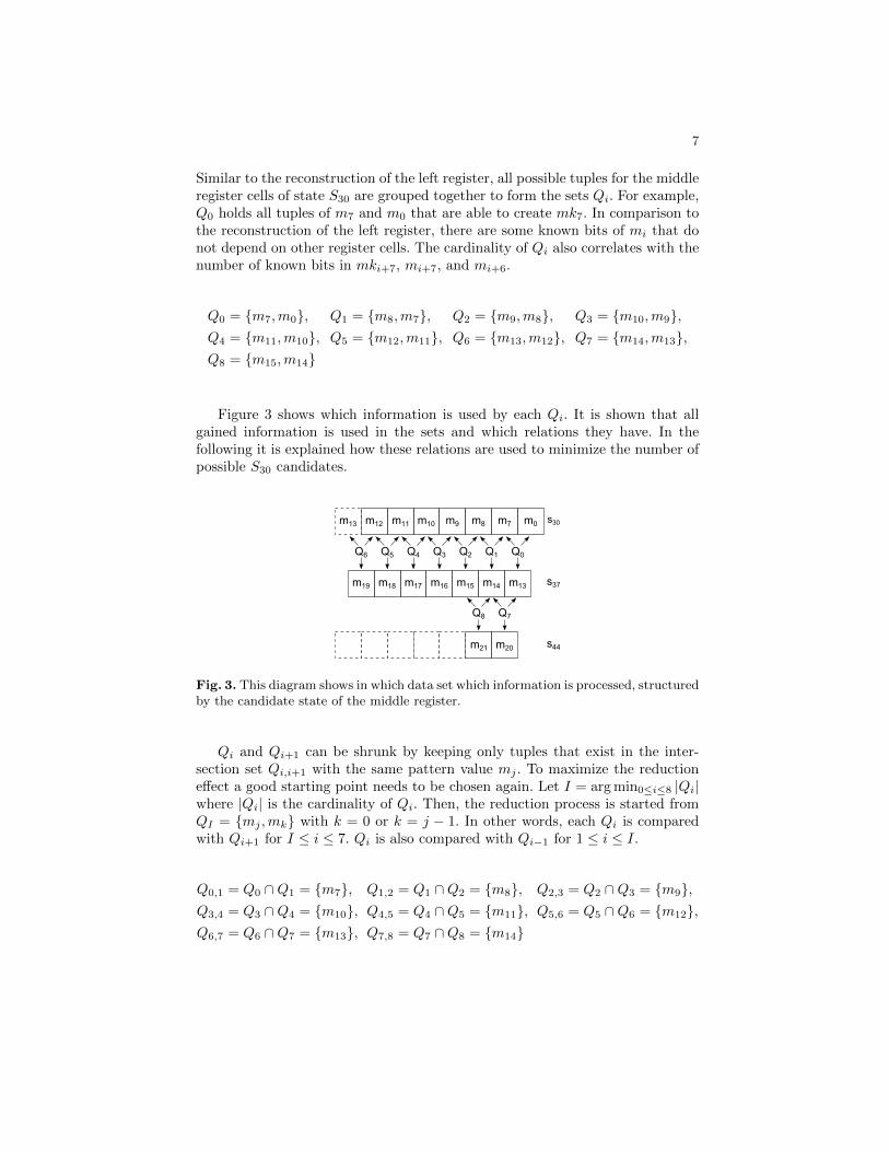
7
Similar to the reconstruction of the left register, all possible tuples for the middleregister cells of state S30 are grouped together to form the sets Qi. For example,Q0 holds all tuples of m7 and m0 that are able to create mk7. In comparison tothe reconstruction of the left register, there are some known bits of mi that donot depend on other register cells. The cardinality of Qi also correlates with thenumber of known bits in mki+7, mi+7, and mi+6.
Q0 = {m7,m0}, Q1 = {m8,m7}, Q2 = {m9,m8}, Q3 = {m10,m9},Q4 = {m11,m10}, Q5 = {m12,m11}, Q6 = {m13,m12}, Q7 = {m14,m13},Q8 = {m15,m14}
Figure 3 shows which information is used by each Qi. It is shown that allgained information is used in the sets and which relations they have. In thefollowing it is explained how these relations are used to minimize the number ofpossible S30 candidates.
m12 m11 m10 m9 m0m8 m7m13 s30
m14 m13m18 m17 m16 m15m19 s37
m21 m20 s44
Q0Q1Q2Q3Q4Q5Q6
Q7Q8
Fig. 3. This diagram shows in which data set which information is processed, structuredby the candidate state of the middle register.
Qi and Qi+1 can be shrunk by keeping only tuples that exist in the inter-section set Qi,i+1 with the same pattern value mj . To maximize the reductioneffect a good starting point needs to be chosen again. Let I = arg min0≤i≤8 |Qi|where |Qi| is the cardinality of Qi. Then, the reduction process is started fromQI = {mj ,mk} with k = 0 or k = j − 1. In other words, each Qi is comparedwith Qi+1 for I ≤ i ≤ 7. Qi is also compared with Qi−1 for 1 ≤ i ≤ I.
Q0,1 = Q0 ∩Q1 = {m7}, Q1,2 = Q1 ∩Q2 = {m8}, Q2,3 = Q2 ∩Q3 = {m9},Q3,4 = Q3 ∩Q4 = {m10}, Q4,5 = Q4 ∩Q5 = {m11}, Q5,6 = Q5 ∩Q6 = {m12},Q6,7 = Q6 ∩Q7 = {m13}, Q7,8 = Q7 ∩Q8 = {m14}
8
Now, the reduced Qi sets are combined to fill the middle register cells six downtothree of state S30. This partially filled register is checked immediately by
mk14 = (m14 ⊕ bS36) � L(m13 ⊕ bS35
) = (m8 � L(m7)) � L(m7 � L(m0)),
mk15 = (m15 ⊕ bS37) � L(m14 ⊕ bS36
) = (m9 � L(m8)) � L(m8 � L(m7)).
This verification is performed by calculating m13, m14 and m15 from m0, m7,m8, and m9. Then the new calculated values are XORed with their feedback byteand it is checked if the tuple (m14, m13) is included in Q7 and if the tuple (m15,m14) is a part of Q8. If this is not the case, the partial candidate is discardedand register cells 3 to 6 are filled with the next combination. Otherwise, cell 2to 0 are filled from Q3, Q4, and Q5 in the same way like cell 3 and 4 to completethe register candidate of state S30. In order to get full cipher candidates of thesame state the middle register is clocked backwards to state S24.
As the final step of the state recovering process, the complete internal stateS24 = (l,m, r, f) is clocked backwards to state S8 and the corresponding outputis compared with ar13 to ar0. This final step usually filters all invalid candidates.A correct state S8 of a frame only persists if it was previously not discarded bythe correlation tests performed on the right and left register candidates.
2.4 RIVYERA Special-Purpose Hardware Cluster
In this work we employ the reconfigurable RIVYERA computing cluster systemwhich is specially designed to process cryptanalytic tasks. The Redesign of the In-credibly Versatile Yet Energy-efficient, Reconfigurable Architecture (RIVYERA)cluster is populated with 128 Spartan-3 XC3S5000 Field Programmable Gate Ar-rays (FPGAs) distributed over 16 card modules. The modules are plugged intoa backplane that provides a systolic ring bus interconnect for high-performancecommunication. Additionally, a host PC is attached to the ring bus via PCI Ex-press and both systems are installed in a 19” rackmount system [10,11,18,19].
3 Advanced Candidate Filtering
The attack described previously creates candidates for each register sequentially.The candidates for the left register are chosen from the output stream of a rightregister candidate, and the middle register candidates are based on the outputstream of a left and a right register candidate. The output function of the left andthe right register is a simple XOR. The XOR operation of the binary complementx0 and x1 of an arbitrary x0 and x1 results in the same output y.
The update function of both register acts as following:
l3 � L(l6) = l0 r2 � r4 = r0 (1)
l3 � L(l6) = l0 when l3 6= L(l6) r2 � r4 = r0 when r2 6= r4 (2)
The probability that the condition in Equation (2) is not given for a register is132 . To create the output stream the right register candidate is clocked 16 times.

9
So the probability that the condition is not met during this time is (1− 132 )16 =
0.6017. Summarizing the previous facts leads to a 60% chance that r as well asr produce the same output stream. In case r passes the correlation test, r passesthe correlation test as well. This behavior also occurs for left register candidates.Due to the fact that the left register candidates are only based on the cipheroutput stream and the right register output stream, r and r produce the sameleft register candidate list. The middle register candidates are also based onlyon the output streams lk and rk which means that the tuples (l, r), (l, r), (l, r)and (l, r) produces the same middle register candidate list, when the conditionsin Equation (2) are satisfied during register output generation.
The attack performs inverted cipher ticks for a register candidate triple(l,m, r) and checks whether it matches to the known ari nibbles. For an in-verted cipher tick a modular subtraction is necessary which is defined as follows:
Definition 8. The modular subtraction operator � : Fn2 × Fn
2 → Fn2 is defined
as:
x� y =
{x− y( mod 2n − 1) if x 6= y
2n − 1 or 0 otherwise
Note that the modular subtraction is non-injective. In case of x = y, the resultof the modular subtraction can be 0 or 2n− 1. The attack, should consider bothcases; in the later steps the wrong guess will be filtered out when not matchingwith ari.
For the modulo subtraction we observe a similar behavior as for the moduloaddition. The condition in Equation (3) is due to the non-injectivity of theoperator.
l0 � l4 = L(l6) r0 � r3 = r4
l0 � l4 = L(l6) when l0 6= l4 r0 � r3 = r4 when r0 6= r3 (3)
Summarizing all these facts leads to the following conclusion. The attackperforms inverse cipher ticks for the triple (r,m, l) to check its consistency withthe known ari nibbles. If r, r and l, l exist in the list of candidates, we validatethe triples (l,m, r), (l,m, r), (l,m, r) at the same time. Also, if (l,m, r) is notthe correct internal state, (l,m, r), (l,m, r), and (l,m, r) will not be the correctone either. Therefore, we can remove l and r from the list of candidates whichgenerate the same output stream as l and r. For a remaining candidate S8 thecomplementary left and right register candidates have to be checked separately ifthey are feasible as well. Our experiments have shown that with this additionalfiltering the number of right and left register candidates are reduced to 68%.In total we only process – on average – 46.24% of the original left and rightcandidate list.
10
4 Mapping Components to Hardware
Most parts of the attack will be executed in software and only the most time-consuming parts are mapped to hardware. In this context, the interfaces betweensoftware and hardware are of major importance to allow a smooth transitionof data in both directions. As a first step we implement the calculations of themiddle register reconstruction process in hardware. The transition from softwareto hardware at this point requires only a very limited number of data transfers.Moreover, this is indeed the most time-consuming part (about 98.8 % of theattack time).
Attacking m begins with the reconstruction of Qi and searches for the small-est set. The subsequent reduction on this step compares possible register cellcandidates. In our hardware implementation we should merge these two steps sothat the generation and reduction of the register cell candidates are performedat once. In order to check whether mi is part of Qj and Qj+1 it is necessary tocheck if (a) mi contains the known bits from the fragmentary middle registeroutput stream and (b) there must be at least one mi+1 and one mi−1 each ofwhich contains the fragmentary known bits and is not removed. Each of themalso must be able to create in conjunction with mi an arbitrary mk+1 and mk,respectively, that each contains the corresponding known bits. If both conditionsare fulfilled, mi is a valid register cell candidate.
Due to our merging technique we do not know which set is the smallestone. So we always start the generation with Q8 and continue the calculationiteratively until we have created Q0. With Q0 we perform the generation andreduction steps again for all sets from Q0 to Q8. During the creation of the sets,either register cell candidates from previously generated sets are used or thecandidates are generated with the help of the known mki bits as described inSection 5.1.
After generation the valid tuples need to be stored in memory. One problemis that we do not know in advance how many valid tuples we will receive but wehave to allocate a fixed amount of memory in hardware. So we assume the worstcase memory complexity for the Qi sets: 27 ·27 ·14 ·9 bits. This translates to 126Block Random-Access Memory (BRAM) blocks with 18kB each, but a Spartan-35000 only provides 108 BRAMs. Due to the sequential nature of the reduction,an on-the-fly calculation of the candidates will result in an enormous increaseof time. An alternative method is to store the information of valid tuples inrelation matrices. In a relation matrix the information of the register cell valuesis encoded in the position of a special flag which indicates if the register cellcombination is valid or not. The usage of relation matrices reduces the memorycomplexity to: 27 · 27 · 9 bits, which needs in total only 9 BRAM blocks tohold the necessary information. This storage method directly leads to the nextchallenge: the efficient reconstruction of register cell values. Obviously, due tothe cell candidate dependencies a bitwise search for each candidate is ineffective.
Finally, the hardware instantiation of an Inverse Cipher Tick (ICT) is nottrivial as well. Each modular subtraction for an ICT is non-injective so for somevalues the result is ambiguous and incorrect values need to be sorted out a few

11
ICTs later. This backtracking behavior complicates a straightforward hardwareimplementation using parallelism or pipelining techniques so that we decided toimplement multiple iterative ICT modules instead for maximum performance.
5 Implementation
In this section we give an overview of the hardware implementation of the attackincluding advanced candidate filtering. Each of the 128 FPGAs is configured withthe same configuration. The design contains two independent attack cores towhich a controller forwards data depending on which module is waiting for a newdataset. Each attack component contains a module to generate Qi tables thatiteratively creates register cell candidates and stores them in the BRAMs. Then,a module reconstructs complete middle register candidates from the previouslygenerated relation matrices (Buffered Pipeline) and distributes the candidates toa free ICT module. The ICT module performs inverse cipher ticks and validatesthe candidate by examining its compliance with ari. Figure 4 depicts the top-level design of our implementation.
ICT S24 to S8
GenerateQi Tables
BufferedPipelineRIVYERA
InterfaceController
ICT S24 to S8
ICT S24 to S8
ICT S24 to S8
ICT S24 to S8
Q0
Q1
Q2
Q8
Attack Core
Attack Core
Fig. 4. The top-level design of our hardware implementation.
5.1 Generating Qi Tables
The Qi generating module iteratively fills Qi with valid register cell tuples andstarts with Q8. First, the design uses just a counter and the partial reconstructedoutput stream to reduce the amount of possible candidates form15,m14 andm13.The possible register cell candidates are then fed into a modular adder thatcalculates m21 and m20 which are directly verified by the known bits. Based onthe results, a BRAM block for Q8 is filled with a stream of bits that representsvalid tuples for m15 and m14. After the calculation of Q8 is completed, themodule continues with the calculation of Q7. At this point possible previouslydefined candidates for m14 are present in memory and the module repeats thesesteps until Q0 is generated. Next it performs the same procedure again in the

12
reverse direction, i.e., from Q1 to Q8 to achieve a maximum effect reducing thenumber of possible register cell candidates. Figure 5 shows an overview of thestructure of the module.
Modular Addition
Modular Addition
ValidationCounter127 to 0
Counter127 to 0
ValidationValidation
Port Multiplexer
Validation Validation
mi
Memory(BRAM)
FF Buffer
Port Multiplexer
Q0
Q8
mimi+1 mi-1
Fig. 5. Design of the Qi generation module.
5.2 Buffered Pipeline
The goal of this unit is to efficiently extract complete middle register candidatesfrom Qi within the BRAM memory. In most cases the relation matrices in mem-ory are rarely filled and a challenge is to find the bits set in Qi and decode theircorresponding position one after another.
In order to decode the position of a set bit in a block a priority decoder canbe used. However for a large blocksize, e.g., 32-bit, the complexity of the prioritydecoder grows enormously requiring a lot of resources. To save the resources wefilter one set bit out of the block and use a simple decoder to extract the positionof this single set bit. The filtering is realized with the following approach:
Let α be a binary block. Instead of using a priority decoder one can calculateα ∧ (α ⊕ (α − 1)) which contains at most a single one bit and passes this toa binary decoder. This process can be iteratively repeated by replacing α byα⊕ (α ∧ (α⊕ (α− 1))). For clarification an example is given in the following:
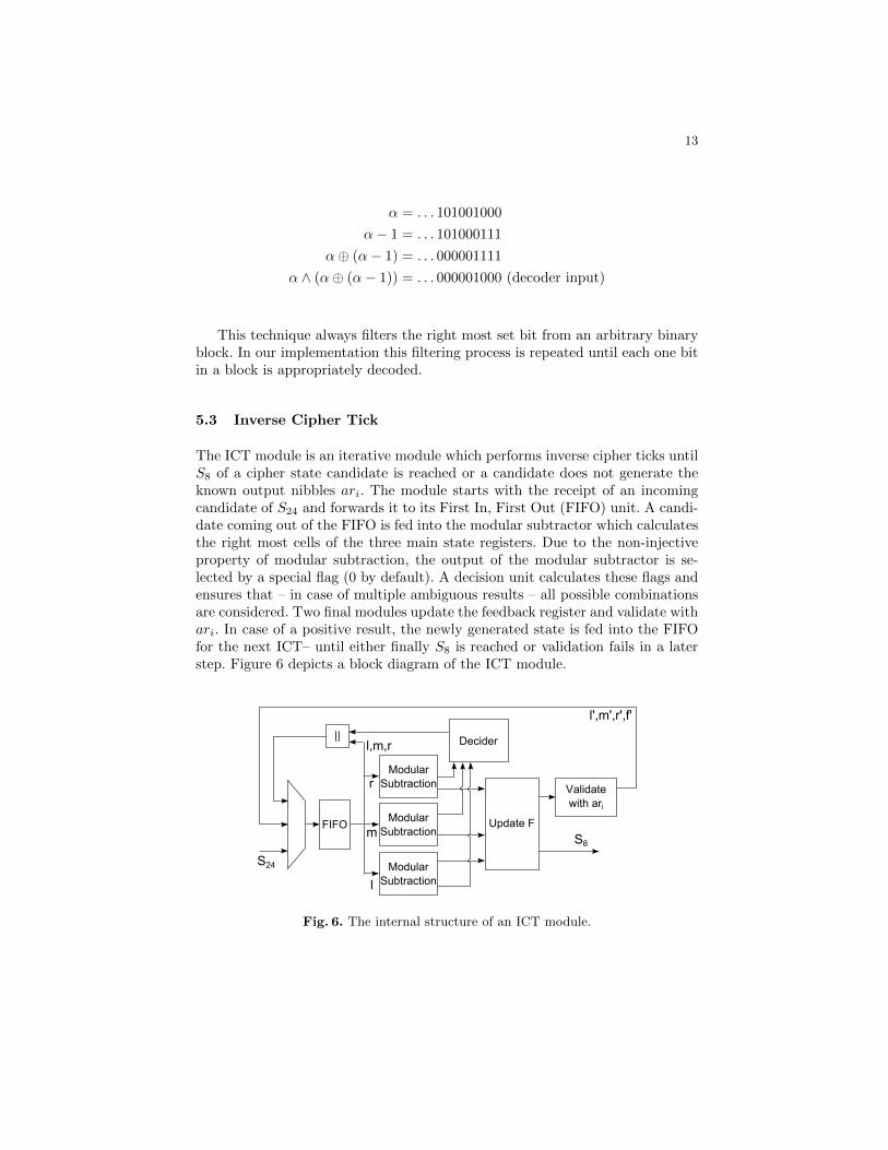
13
α = . . . 101001000
α− 1 = . . . 101000111
α⊕ (α− 1) = . . . 000001111
α ∧ (α⊕ (α− 1)) = . . . 000001000 (decoder input)
This technique always filters the right most set bit from an arbitrary binaryblock. In our implementation this filtering process is repeated until each one bitin a block is appropriately decoded.
5.3 Inverse Cipher Tick
The ICT module is an iterative module which performs inverse cipher ticks untilS8 of a cipher state candidate is reached or a candidate does not generate theknown output nibbles ari. The module starts with the receipt of an incomingcandidate of S24 and forwards it to its First In, First Out (FIFO) unit. A candi-date coming out of the FIFO is fed into the modular subtractor which calculatesthe right most cells of the three main state registers. Due to the non-injectiveproperty of modular subtraction, the output of the modular subtractor is se-lected by a special flag (0 by default). A decision unit calculates these flags andensures that – in case of multiple ambiguous results – all possible combinationsare considered. Two final modules update the feedback register and validate withari. In case of a positive result, the newly generated state is fed into the FIFOfor the next ICT– until either finally S8 is reached or validation fails in a laterstep. Figure 6 depicts a block diagram of the ICT module.
ModularSubtraction
Modular Subtraction
ModularSubtraction
FIFO
Decider
Update F
Validate with ari
||
l
m
r
l,m,r
l',m',r',f'
S24
S8
Fig. 6. The internal structure of an ICT module.

14
6 Results
In this section we present the results of our hardware implementation obtainedusing Xilinx ISE Foundation 14.3 for synthesis and place and route. The designwith two attack cores of which each contains 17 ICT modules is synthesized andruns at the frequency of 100MHz. The utilized resources on each Spartan-3 5000are shown in Table 1.
Essentially, the attack speed strongly depends on the frequency of operationand the number of attack components and ICT modules per core. The integratedFIFO component of each module has a data width of 125 bits which results inthe utilization of 4 BRAM primitives on a Spartan-3. The complete hardwaredesign is limited by BRAM blocks, i.e., a generic design configuration with twoattack cores based on BRAM can only instantiate 7 ICT modules per core. Fora better resource utilization a dedicated LUT-based version of the ICT moduleswas generated to instantiate the internal FIFO. This alternative implementationallows us to instantiate 10 additional ICT modules per core. Table 1 shows theresource consumptions of both ICT versions on a Spartan-3 5000.
Table 1. Resource consumption of a dedicated RAM-based ICT BRAM-based ICTand for the complete design (two attack components and 17 ICT) on a Spartan-3 5000FPGA
Resource DRAM ICT BRAM ICT Complete Available
Slices 808 482 28.298 33.280Lookup Tables (LUTs) 1058 469 45.600 66.560
Slice Registers 460 317 28.199 66.560BRAM 0 4 103 104
Next we compare the throughput of the CPU-based cluster implementationin [4] with our hardware implementation on RIVYERA. Note that exact cyclecounts are not available for the implementation given in [4]. Therefore we restrictour comparison to the data as shown in Table 2.
In order to determine the attack speed of our solution, we measure the val-idation time for a left and right register pair. 300 randomly generated framesare chosen to compute the average time needed for register pair validation. Onaverage one attack unit is able to check one left/right register candidate tuplein 0.8 seconds. To have a 50% chance for a successful attack we need 30 framessimilarly as stated in [4]. On average 23 right and 219.527 left register candidatesare generated out of 30 frames what leads to a total running time of the attackto reconstruct the internal state in about 13 hours (0.55 days).
Apart from performance, the cost for running an attack is of utmost impor-tance. The CPU-based attack was run on a rented Amazon Elastic ComputeCloud (EC2) cluster but unfortunately, RIVYERA is not for rent. For a faircomparison, we therefore compare the running costs of the attack by estimating

15
Table 2. Comparison between the RIVYERA and CPU cluster implementation.
Aspect RIVYERA CPU
Parallelization 128 FPGAs with 200 CPU cores2 attack coresand 17 ICT
Clock Cycles per ICT step 5 27
Clock Frequency [GHz] 0.1 2.26Candidate Reduction (l/r) 0.4624 1Total Time [days] 0.55 2+6
2= 4
Total improvement factor 40.55
= 7.27 1Performance equivalency 1 FPGA ≡ 11.36 CPUs
Power Consumption per Device [KW] 0.65 2.56Power Consumption per Attack [KWh] 0.65 · 13.23 = 8.6 2.56 · 96 = 245.76Cost Reduction 28.58 1
the power consumption for both attack implementations. The RIVYERA S-35000 takes on average 650W while two Intel Xeon L5640 CPUs including pe-ripherals approximately demand (60W · 2) + 40W = 160W [12] for the completesystem. To run the attack in the given time as stated in [4], at least 16 such com-puting systems are required. The power consumption in Table 2 shows again theadvantage of special-purpose hardware over CPU-based attack clusters.
Despite the performance improvement with the Spartan-3 5000, we can achieveeven higher performance with later FPGA devices. In particular, the RIVYERAS6-LX150 which can be equipped with 256 Spartan-6 LX150 offers by far morelogic and performance but was not available in the course of this work. However,to provide at least estimates, we adapted our design for the Spartan-6 LX150 onwhich we can instantiate the double amount of attack cores with 17 ICT moduleseach. Additionally, we can run the design at double clock frequency due to thenewer FPGA technology (200MHz) which results in an additional performancespeed-up by factor of four.
7 Conclusion
The hardware implementation presented in this work improves the attack onCryptoMemory devices by Biryukov et al. [4] by introducing an additional can-didate filtering step reducing the computation complexity to a half. By mappingthe most time consuming parts to FPGA hardware, our solution runs in total7.27 times faster than the previously reported results using 30 authenticationframes. This enables the complete recovery of the secret internal state of theCryptoMemory cipher on average in less than 0.55 days. Finally, our hardwareattack is 28.58 times cheaper considering power consumption compared to [4]using a CPU-based cluster.
16
Acknowledgements. The authors would like to thank Alex Biryukov, IlyaKizhvatov and Bin Zhang for useful discussions and for their kindness providingparts of their attack script.
References
1. Atmel Corporation. CryptoMemory for Removable Storage Devicesand Reprogrammable Keys. http://www.cryptomemorykey.com/pdfs/
AtmelCryptoMemoryFlier.pdf, as of April 19, 2013.2. Atmel Corporation. CryptoMemory specification. http://www.atmel.com/
Images/doc5211.pdf, as of April 19, 2013, 2007.3. J. Balasch, B. Gierlichs, R. Verdult, L. Batina, and I. Verbauwhede. Power Analysis
of Atmel CryptoMemory - Recovering Keys from Secure EEPROMs. In CT-RSA2012, volume 7178 of LNCS, pages 19–34. Springer, 2012.
4. A. Biryukov, I. Kizhvatov, and B. Zhang. Cryptanalysis of the Atmel Cipher inSecureMemory, CryptoMemory and CryptoRF. In ACNS 2011, volume 6715 ofLNCS, pages 91–109. Springer, 2011.
5. A. Biryukov, I. Kizhvatov, and B. Zhang. Cryptanalysis of The Atmel Cipher inSecureMemory, CryptoMemory and CryptoRF. IACR Cryptology ePrint Archive,page 22, 2011.
6. Digitrade GmbH. http://www.digittrade.de/shop/index.php/cat/c66_
HS256S-High-Security.html.7. B. Dipert. The Zune HD: more than an iPod touch wanna-be? EDN, 2009.8. F. Garcia, P. van Rossum, R. Verdult, and R. Wichers Schreur. Dismantling Se-
cureMemory, CryptoMemory and CryptoRF. In CCS 2010, pages 250–259. ACM,2010.
9. M. Giacomelli. SanDisk Sansa Connect. http://www.rockbox.org/wiki/
SansaConnect.10. T. Guneysu, T. Kasper, M. Novotny, C. Paar, and A. Rupp. Cryptanalysis with
COPACOBANA. IEEE Transactions on Computers, 57(11):1498–1513, 2008.11. T. Guneysu, G. Pfeiffer, C. Paar, and M. Schimmler. Three Years of Evolution:
Cryptanalysis with COPACOBANA. In SHARCS 2009, pages 9–10, 2009.12. Intel. Intel Xeon Processor 5600 Series: Product Brief. Available
via http://www.intel.com/content/dam/www/public/us/en/documents/
product-briefs/xeon-5600-brief.pdf.13. M. Jarboe. Introduction to CryptoMemory. Atmel Applications Journal, 3:28,
2004.14. S. Jozsef. AT88SC0204 ChipResetter. http://chipreset.atw.hu/6/index61.
html.15. Labgear. Labgear HDSR300 High Definition Satellite Receiver. User Guide. http:
//www.free-instruction-manuals.com/pdf/p4789564.pdf, as of April 19, 2013.16. NVIDIA Corporation. Checklist for Building a PC that Plays HD DVD or
Blue-ray Movies. ftp://download.nvidia.com/downloads/pvzone/Checklist_
for_Building_a_HDPC.pdf, as of April 19, 2013.17. SciEngines GmbH. http://www.sciengines.com.18. Xilinx. Spartan-3 FPGA Family: Complete Data Sheet. Product Documentation,
November 2005.19. Xilinx. Spartan-3 Generation FPGA User Guide. Product Documentation, June
2011.