atwinc3400-ieee® 802.11 b/g/n network controller...
TRANSCRIPT

ATWINC3400-MR210CA IEEEreg 80211 bgn Network Controller Module with
Integrated Bluetoothreg Low Energy 40
Introduction
The ATWINC3400-MR210CA is an IEEE 80211 bgn RFBasebandMedium Access Control (MAC)network controller module with Bluetooth Low Energy technology that is compliant with Bluetooth version40 This module is optimized for low power and high performance mobile applications This modulefeatures small form factor when integrating Power Amplifier (PA) Low-Noise Amplifier (LNA) TransmitReceive (TR) switch (for Wi-Fireg and Bluetooth) Power Management Unit (PMU) and Chip Antenna TheATWINC3400-MR210CA module requires a 32768 kHz clock for Sleep operation
The ATWINC3400-MR210CA module utilizes highly optimized IEEE 80211 Bluetooth coexistenceprotocols and provides Serial Peripheral Interface (SPI) to interface with the host controller
Features
Wi-Fi features
bull IEEE 80211 bgn RFPHYMACbull IEEE 80211 bgn (1x1) with single spatial stream up to 72 Mbps PHY rate in 24 GHz ISM bandbull Integrated chip antennabull Superior sensitivity and range via advanced PHY signal processingbull Advanced equalization and channel estimationbull Advanced carrier and timing synchronizationbull Supports Soft-APbull Supports IEEE 80211 WEP WPA and WPA2bull Superior MAC throughput through hardware accelerated two-level A-MSDUA-MPDU frame
aggregation and block acknowledgmentbull On-chip memory management engine to reduce the host loadbull Operating temperature range from -40degC to +85degCbull Wi-Fi Alliancereg certified for connectivity and optimizations
ndash ID WFA62065bull Integrated on-chip microcontrollerbull SPI host interfacebull Integrated Flash memory for Wi-Fi and Bluetooth system softwarebull Low leakage on-chip memory for state variablesbull Fast AP re-association (150 ms)bull On-chip network stack to offload MCU
ndash Integrated network IP slack to minimize the host CPU requirements
copy 2017 Microchip Technology Inc Datasheet Preliminary DS70005350A-page 1
bull Network features Firmware version 12xndash TCP UDP DHCP ARP HTTP SSL DNS and SNTP
Bluetooth features
bull Bluetooth 40 (Bluetooth Low Energy) certificationsndash Controller QD ID - 77870ndash Host QD ID - 77451
bull Adaptive Frequency Hopping (AFH)bull Superior sensitivity and range
ATWINC3400-MR210CA
copy 2017 Microchip Technology Inc Datasheet Preliminary DS70005350A-page 2
Table of Contents
Introduction1
Features 1
1 Ordering Information and Module Marking 5
2 Block Diagram 6
3 Pinout and Package Information 731 Package Description 10
4 Electrical Characteristics1141 Absolute Maximum Ratings1142 Recommended Operating Conditions 1143 DC Characteristics 1244 IEEE 80211 bgn Radio Performance 1245 Bluetooth Radio Performance 1446 Timing Characteristics16
5 Power Management 2151 Device States 2152 Controlling Device States2153 Power-UpDown Sequence2254 Digital IO Pin Behavior During Power-Up Sequences23
6 Clocking2461 Low-Power Clock 24
7 CPU and Memory Subsystem 2571 Processor 2572 Memory Subsystem2573 Nonvolatile Memory25
8 WLAN Subsystem 2781 MAC 2782 PHY2883 Radio28
9 Bluetooth Low Energy 40 30
10 External Interfaces31101 Interfacing with the Host Microcontroller 31102 SPI Interface32103 UART Interface34
copy 2017 Microchip Technology Inc Datasheet Preliminary DS70005350A-page 3
11 Application Reference Design 36111 Host Interface - SPI36
12 Module Outline Drawings 38
13 Design Consideration 39131 Module Placement and Routing Guidelines 39132 Antenna Performance 40
14 Reflow Profile Information 42141 Storage Condition42142 Solder Paste42143 Stencil Design 42144 Baking Conditions 42145 Soldering and Reflow Condition42
15 Module Assembly Considerations 45
16 Regulatory Approval46161 United States46162 Canada47163 Europe49164 Other Regulatory Information50
17 Reference Documentation51
18 Document Revision History 52
The Microchip Web Site 53
Customer Change Notification Service53
Customer Support 53
Microchip Devices Code Protection Feature 53
Legal Notice54
Trademarks 54
Quality Management System Certified by DNV55
Worldwide Sales and Service56
ATWINC3400-MR210CA
copy 2017 Microchip Technology Inc Datasheet Preliminary DS70005350A-page 4
1 Ordering Information and Module MarkingThe following table provides the ordering details for the ATWINC3400-MR210CA module
Table 1-1 Ordering Details
Model Number Ordering Code Package Description RegulatoryInformation
ATWINC3400-MR210CA
ATWINC3400-MR210CAxxx 1
2243 x1473 x 20mm
Certifiedmodule withchip antenna
FCC IC CE
Note 1 xxx in the preceding table and following figure denotes the software version For example at the
time of publish the software is v122 so its equivalent order code is ATWINC3400-MR210CA122The order code changes as per the software version For more information on ordering code referto the ATWINC3400-MR product page
The following figure illustrates the ATWINC3400-MR210CA module marking information
Figure 1-1 Marking Information
MR 2 1 0 C
Device name
MR Industrial
2 OTA with shield
1 Reserved
0 Reserved
C Chip antenna
Revision letter
Software version
ATWINC3400 A xxx
ATWINC3400-MR210CAOrdering Information and Module Marking
copy 2017 Microchip Technology Inc Datasheet Preliminary DS70005350A-page 5
2 Block DiagramThe following figure shows the block diagram of the ATWINC3400-MR210CA moduleFigure 2-1 ATWINC3400-MR210CA Module Block Diagram
ATWINC3400 IC
ATWINC3400-MR210CABlock Diagram
copy 2017 Microchip Technology Inc Datasheet Preliminary DS70005350A-page 6
3 Pinout and Package InformationThis package contains an exposed paddle that must be connected to the system board ground TheATWINC3400-MR210CA module pin assignment is shown in following figureFigure 3-1 ATWINC3400-MR210CA Module Pin Assignment
ATWINC3400-MR210CAMODULEJ1
J2
J3
J4
J5
J6
J7
J8
J9
J10
J11
J12J13
J14
J15
J16
J17
J18
J19
J20
J21
J22
J23
J24
J25J26
J27
J28
J29
J30
J31
J32
J33
J34
J35
J36 GND
I2C_SDA_M
I2C_SCL_M
IRQN
GPIO20
GPIO19
GPIO18
GPIO17
GND
GPIO7
SPI_MOSI
SPI_SSN
SPI_
MIS
O
SPI_
SCK
GPI
O8
GN
D
RTC
_CLK
CH
IP_E
N
VBAT
UA
RT_
RXD
UA
RT_
TXD
GPI
O4
GPI
O3
GND
VDDIO
BT_RXD
BT_TXD
RESETN
NC
NC
NC
NC
SPI_CFG
GND
I2C_SDA_S
I2C_SCL_S
The following table provides the ATWINC3400-MR210CA module pin description
ATWINC3400-MR210CAPinout and Package Information
copy 2017 Microchip Technology Inc Datasheet Preliminary DS70005350A-page 7
Table 3-1 ATWINC3400-MR210CA Module Pin Description
Pin Pin Name Pin Type Description
1 GND GND Ground pin
2 SPI_CFG Digital Input Serial Peripheral Interface pin which must betied to VDDIO
3 NC - No connection
4 NC - No connection
5 NC - No connection
6 NC - No connection
7 RESETN Digital Input bull Active-low hard Reset pinbull When the Reset pin is asserted low the
module is in the Reset state When theReset pin is asserted high the modulefunctions normally
bull This pin must connect to a host outputthat is low by default on power-up If thehost output is tri-stated add a 1 MOhmpull down resistor to ensure a low level atpower-up
8 BT_TXD Digital IOProgrammable pull up
Bluetooth UART transmit data output pin
9 BT_RXD Digital IOProgrammable pull up
Bluetooth UART receive data input pin
10 I2C_SDA_S Digital IOProgrammable pull up
bull I2C Slave data pinbull Used only for test purposes It is
recommended to add a test point for thispin
11 I2C_SCL_S Digital IOProgrammable pull up
bull I2C Slave clock pinbull Used only for test purposes It is
recommended to add a test point for thispin
12 VDDIO Power Digital IO power supply
13 GND GND Ground pin
14 GPIO3 Digital IOProgrammable pull up
General Purpose InputOutput pin
15 GPIO4 Digital IOProgrammable pull up
General Purpose InputOutput pin
16 UART_TXD Digital IOProgrammable pull up
bull Wi-Fi UART TxD output pin
ATWINC3400-MR210CAPinout and Package Information
copy 2017 Microchip Technology Inc Datasheet Preliminary DS70005350A-page 8
Pin Pin Name Pin Type Description
bull Used only for debug developmentpurposes It is recommended to add atest point for this pin
17 UART_RXD Digital IOProgrammable pull up
bull Wi-Fi UART RxD input pinbull Used only for debug development
purposes It is recommended to add atest point for this pin
18 VBAT Power Power supply pin for DCDC converter and PA
19 CHIP_EN Digital Input bull PMU enable pinbull When the CHIP_EN pin is asserted high
the module is enbled When theCHIP_EN pin is asserted low the moduleis disabled or put into Power-Down mode
bull Connect to a host output that is low bydefault at power-up If the host output istri-stated add a 1 MOhm pull downresistor if necessary to ensure a low levelat power-up
20 RTC_CLK Digital IOProgrammable pull up
bull RTC Clock input pinbull This pin must connect to a 32768 kHz
clock source
21 GND GND Ground pin
22 GPIO8 Digital IOProgrammable pull up
General Purpose InputOutput pin
23 SPI_SCK Digital IOProgrammable pull up
SPI clock pin
24 SPI_MISO Digital IOProgrammable pull up
SPI MISO (Master In Slave Out) pin
25 SPI_SSN Digital IOProgrammable pull up
Active-low SPI SSN (Slave Select) pin
26 SPI_MOSI Digital IOProgrammable pull up
SPI MOSI (Master Out Slave In) pin
27 GPIO7 Digital IOProgrammable pull up
General Purpose InputOutput pin
28 GND GND Ground pin
29 GPIO17 Digital IOProgrammable pull up
General Purpose InputOutput pin
30 GPIO18 Digital IOProgrammable pull up
General Purpose InputOutput pin
ATWINC3400-MR210CAPinout and Package Information
copy 2017 Microchip Technology Inc Datasheet Preliminary DS70005350A-page 9
Pin Pin Name Pin Type Description
31 GPIO19 Digital IOProgrammable pull up
General Purpose InputOutput pin
32 GPIO20 Digital IOProgrammable pull up
General Purpose InputOutput pin
33 IRQN Digital outputProgrammable pull up
bull ATWINC3400-MR210CA module hostinterrupt request output pin
bull This pin must connect to a host interruptpin
34 I2C_SCL_M Digital IOProgrammable pull up
I2C Master clock pin
35 I2C_SDA_M Digital IOProgrammable pull up
I2C Master data pin
36 GND GND Ground pin
37 PADDLE VSS Power Connect to system board ground
31 Package DescriptionThe following table provides the ATWINC3400-MR210CA module package dimensions
Table 3-2 ATWINC3400-MR210CA Module Package Information
Parameter Value Unit
Pad count 36 -
Package size 2243 x 1473 mm
Total thickness 209
Pad pitch 120
Pad width 081
Exposed pad size 44 x 44
ATWINC3400-MR210CAPinout and Package Information
copy 2017 Microchip Technology Inc Datasheet Preliminary DS70005350A-page 10
4 Electrical CharacteristicsThis chapter provides an overview of the electrical characteristics of the ATWINC3400-MR210CAmodule
41 Absolute Maximum RatingsThe following table provides the absolute maximum ratings for the ATWINC3400-MR210CA module
Table 4-1 ATWINC3400-MR210CA Module Absolute Maximum Ratings
Symbol Parameter Min Max Unit
VDDIO IO supply voltage -03 50 V
VBAT Battery supply voltage -03 50
VIN Digital input voltage -03 VDDIO
VAIN Analog input voltage -03 15
VESDHBM Electrostatic dischargeHuman Body Model(HBM)
-1000 -2000 (seenotes below)
+1000 +2000 (seenotes below)
TA Storage temperature -65 150 ordmC
- Junction temperature - 125
- RF input power - 23 dBm
1 VIN corresponds to all the digital pins2 For VESDHBM each pin is classified as Class 1 or Class 2 or both
21 The Class 1 pins include all the pins (both analog and digital)22 The Class 2 pins include all digital pins only23 VESDHBM is plusmn1 kV for Class 1 pins VESDHBM is plusmn 2 kV for Class 2 pins
CAUTION Caution Stresses beyond those listed under ldquoAbsolute Maximum Ratingsrdquo cause permanentdamage to the device This is a stress rating only The functional operation of the device atthose or any other conditions above those indicated in the operation listings of this specificationis not implied Exposure to maximum rating conditions for extended periods affects the devicereliability
42 Recommended Operating ConditionsThe following table provides the recommended operating conditions for the ATWINC3400-MR210CAmodule
ATWINC3400-MR210CAElectrical Characteristics
copy 2017 Microchip Technology Inc Datasheet Preliminary DS70005350A-page 11
Table 4-2 ATWINC3400-MR210CA Module Recommended Operating Conditions
Symbol Parameter Min Typ Max Units
VDDIO IO supply voltage (1) 27 33 36 V
VBAT Battery supply voltage(2)(3) 30 36 42 V
- Operating temperature -40 - 85 ordmC
Note 1 IO supply voltage is applied to the VDDIO pin2 Battery supply voltage is applied to the VBAT pin3 The ATWINC3400-MR210CA module is functional across this range of voltages however optimal
RF performance is guaranteed for VBAT in the range ge 30V VBAT le 42V
43 DC CharacteristicsThe following table provides the DC characteristics for the ATWINC3400-MR210CA module digital pads
Table 4-3 DC Electrical Characteristics
Symbol Parameter Min Typ Max Unit
VIL Input LowVoltage
-030 - 060 V
VIH Input HighVoltage
VDDIO-060 - VDDIO+030
VOL Output LowVoltage
- - 045
VOH Output HighVoltage
VDDIO-050 - -
- Output LoadCapacitance
- - 20 pF
- Digital InputLoadCapacitance
- - 6
44 IEEE 80211 bgn Radio Performance
441 Receiver PerformanceThe receiver performance is tested under following conditions
bull VBAT = 33Vbull VDDIO = 33Vbull Temp = 25degCbull Measured after RF matching network
The following table provides the receiver performance characteristics for the ATWINC3400-MR210CAmodule
ATWINC3400-MR210CAElectrical Characteristics
copy 2017 Microchip Technology Inc Datasheet Preliminary DS70005350A-page 12
Table 4-4 IEEE 80211 Receiver Performance Characteristics
Parameter Description Min Typ Max Unit
Frequency - 2412 - 2472 MHz
Sensitivity 80211b 1 Mbps DSSS - -950 - dBm
2 Mbps DSSS - -940 -
55 Mbps DSSS - -900 -
11 Mbps DSSS - -860 -
Sensitivity 80211g 6 Mbps OFDM - -900 - dBm
9 Mbps OFDM - -890 -
12 Mbps OFDM - -870 -
18 Mbps OFDM - -850 -
24 Mbps OFDM - -820 -
36 Mbps OFDM - -790 -
48 Mbps OFDM - -750 -
54 Mbps OFDM - -730 -
Sensitivity 80211n(BW=20 MHz800ns GI)
MCS 0 - -890 - dBm
MCS 1 - -870 -
MCS 2 - -840 -
MCS 3 - -820 -
MCS 4 - -780 -
MCS 5 - -750 -
MCS 6 - -730 -
MCS 7 - -710 -
Maximum receivesignal level
1-11 Mbps DSSS - 0 - dBm
6-54 Mbps OFDM - 0 -
MCS 0 - 7 (800ns GI) - 0 -
Adjacent channelrejection
1 Mbps DSSS (30 MHz offset) - 50 - dB
11 Mbps DSSS (25 MHz offset) - 43 -
6 Mbps OFDM (25 MHz offset) - 40 -
54 Mbps OFDM (25 MHz offset) - 25 -
MCS 0 ndash 20 MHz BW (25 MHzoffset)
- 40 -
MCS 7 ndash 20 MHz BW (25 MHzoffset)
- 20 -
ATWINC3400-MR210CAElectrical Characteristics
copy 2017 Microchip Technology Inc Datasheet Preliminary DS70005350A-page 13
442 Transmitter PerformanceThe transmitter performance is tested under following conditions
bull VBAT = 33Vbull VDDIO = 33Vbull Temp = 25degC
The following table provides the transmitter performance characteristics for the ATWINC3400-MR210CAmodule
Table 4-5 IEEE 80211 Transmitter Performance Characteristics
Parameter Description Minimum Typical Max Unit
Frequency - 2412 - 2472 MHz
Output power 80211b 1 Mbps - 167(1) - dBm
80211b 11 Mbps - 175(1) -
80211g OFDM 6 Mbps - 183(1) -
80211g OFDM 54 Mbps - 130(1) -
80211n HT20 MCS 0 (800nsGI)
- 175(1) -
80211n HT20 MCS 7 (800nsGI)
- 125(1) -
Tx power accuracy - - plusmn15(2) - dB
Carrier suppression - - 300 - dBc
Harmonic outputpower (RadiatedRegulatory mode)
2nd - - -41 dBmMHz
3rd - - -41
Note 1 Measured at IEEE 80211 specification compliant EVMSpectral mask2 Measured after RF matching network3 Operating temperature range is -40degC to +85degC RF performance guaranteed at room temperature
of 25degC with a 2-3dB change at boundary conditions4 With respect to Tx power different (higherlower) RF output power settings may be used for specific
antennas andor enclosures in which case recertification may be required5 The availability of some specific channels andor operational frequency bands are country
dependent and should be programmed at the host product factory to match the intendeddestination Regulatory bodies prohibit exposing the settings to the end user This requirementneeds to be taken care of via host implementation
45 Bluetooth Radio Performance
451 Receiver PerformanceThe receiver performance is tested under following conditions
ATWINC3400-MR210CAElectrical Characteristics
copy 2017 Microchip Technology Inc Datasheet Preliminary DS70005350A-page 14
bull VBAT = 33Vbull VDDIO = 33Vbull Temp 25degCbull Measured after RF matching network
The following table provides the Bluetooth receiver performance characteristics for the ATWINC3400-MR210CA module
Table 4-6 Bluetooth Receiver Performance Characteristics
Parameter Description Min Typ Max Unit
Frequency - 2402 - 2480 MHz
Sensitivity (ideal Tx) Bluetooth Low Energy (GFSK) - -925 - dBm
Maximum receive signallevel
Bluetooth Low Energy (GFSK) - -2 -
Interference performance(Bluetooth Low Energy)
Co-channel - 9 dB
adjacent + 1 MHz - -4 -
adjacent - 1 MHz - -2 -
adjacent + 2 MHz(imagefrequency)
- -24 -
adjacent - 2 MHz - -25 -
adjacent + 3 MHz (adjacent toimage)
- -27 -
adjacent - 3 MHz - -27 -
adjacent + 4 MHz - -28 -
adjacent - 4 MHz - -27 -
adjacent +5 MHz - -27 -
adjacent - 5 MHz - -27 -
452 Transmitter PerformanceThe transmitter performance is tested under following conditions
bull VBAT = 33Vbull VDDIO = 33Vbull Temp 25degCbull Measured after RF matching network
The following table provides the Bluetooth transmitter performance characteristics for the ATWINC3400-MR210CA module
ATWINC3400-MR210CAElectrical Characteristics
copy 2017 Microchip Technology Inc Datasheet Preliminary DS70005350A-page 15
Table 4-7 Bluetooth Transmitter Performance Characteristics
Parameter Description Min Typ Max Unit
Frequency - 2402 - 2480 MHz
Output power Bluetooth Low Energy (GFSK) - 33 38 dBm
In-band spuriousemission (Bluetooth LowEnergy)
N+2 (Image frequency) - -33 -
N + 3 (Adjacent to imagefrequency)
- -32 -
N-2 - -48 -
N-3 - -47 -
46 Timing Characteristics
461 I2C Slave TimingThe I2C Slave timing diagram for the ATWINC3400-MR210CA module is shown in the following figure
Figure 4-1 I2C Slave Timing Diagram
The following table provides the I2C Slave timing parameters for the ATWINC3400-MR210CA module
Table 4-8 I2C Slave Timing Parameters
Parameter Symbol Min Max Units Remarks
SCL Clock Frequency fSCL 0 400 kHz -
SCL Low Pulse Width tWL 13 -micros
-
SCL High Pulse Width tWH 06 - -
SCL SDA Fall Time tHL - 300ns
-
SCL SDA Rise Time tLH - 300 This is dictated byexternal components
ATWINC3400-MR210CAElectrical Characteristics
copy 2017 Microchip Technology Inc Datasheet Preliminary DS70005350A-page 16
Parameter Symbol Min Max Units Remarks
START Setup Time tSUSTA 06 -micros
-
START Hold Time tHDSTA 06 - -
SDA Setup Time tSUDAT 100 - ns -
SDA Hold Time tHDDAT
0 - ns Slave and Master Default
40 - micros Master ProgrammingOption
STOP Setup Time tSUSTO 06 -micros
-
Bus Free Time BetweenSTOP and START tBUF 13 - -
Glitch Pulse Reject tPR 0 50 ns -
462 SPI Slave TimingThe SPI Slave timing for the ATWINC3400-MR210CA module is provided in the following figuresFigure 4-2 SPI Slave Clock Polarity and Clock Phase Timing
ATWINC3400-MR210CAElectrical Characteristics
copy 2017 Microchip Technology Inc Datasheet Preliminary DS70005350A-page 17
Figure 4-3 SPI Slave Timing Diagram
The following table provides the SPI Slave timing parameters for the ATWINC3400-MR210CA module
Table 4-9 SPI Slave Timing Parameters (1)
Parameter Symbol Min Max Unit
Clock Input Frequency (2) fSCK - 48 MHz
Clock Low Pulse Width tWL 6 - ns
Clock High Pulse Width tWH 4 -
Clock Rise Time tLH 0 7
Clock Fall Time tHL 0 7
TXD Output Delay (3) tODLY 3 9 from SCK fall11 from SCK rise
RXD Input Setup Time tISU 3 -
RXD Input Hold Time tIHD 5 -
ATWINC3400-MR210CAElectrical Characteristics
copy 2017 Microchip Technology Inc Datasheet Preliminary DS70005350A-page 18
Parameter Symbol Min Max Unit
SSN Input Setup Time tSUSSN 5 -
SSN Input Hold Time tHDSSN 5 -
Note 1 Timing is applicable to all SPI modes2 Maximum clock frequency specified is limited by the SPI Slave interface internal design actual
maximum clock frequency can be lower and depends on the specific PCB layout3 Timing based on 15 pF output loading
463 SPI Master TimingThe SPI Master timing for the ATWINC3400-MR210CA module is shown in the following figureFigure 4-4 SPI Master Timing Diagram
The following table provides the SPI Master timing parameters for the ATWINC3400-MR210CA module
Table 4-10 SPI Master Timing Parameters (1)
Parameter Symbol Min Max Unit
Clock Output Frequency (2) fSCK - 20 MHz
Clock Low Pulse Width tWL 19 - ns
Clock High Pulse Width tWH 21 -
Clock Rise Time (3) tLH - 11
Clock Fall Time (3) tHL - 10
RXD Input Setup Time tISU 24 -
RXD Input Hold Time tIHD 0 -
SSNTXD Output Delay (3) tODLY -5 3
ATWINC3400-MR210CAElectrical Characteristics
copy 2017 Microchip Technology Inc Datasheet Preliminary DS70005350A-page 19
Note 1 Timing is applicable to all SPI modes2 Maximum clock frequency specified is limited by the SPI Master interface internal design actual
maximum clock frequency can be lower and depends on the specific PCB layout3 Timing based on 15 pF output loading
ATWINC3400-MR210CAElectrical Characteristics
copy 2017 Microchip Technology Inc Datasheet Preliminary DS70005350A-page 20
5 Power Management
51 Device StatesThe ATWINC3400-MR210CA module has multiple device states based on the state of the IEEE 80211and Bluetooth subsystems It is possible for both subsystems to be active at the same time To simplifythe device power consumption breakdown the following basic states are defined One subsystem can beactive at a time
bull WiFi_ON_Transmit ndash Device actively transmits IEEE 80211 signalbull WiFi_ON_Receive ndash Device actively receives IEEE 80211 signalbull BT_ON_Transmit ndash Device actively transmits Bluetooth signalbull BT_ON_Receive ndash Device actively receives Bluetooth signalbull Doze ndash Device is powered on but it does not actively transmit or receive databull Power_Down ndash Device core supply is powered off
52 Controlling Device StatesThe following table shows different device states and its power consumption The device states can beswitched using the following
bull CHIP_EN ndash Module pin (pin 19) enables or disables the DCDC converterbull VDDIO ndash IO supply voltage from external supply
In the ON states VDDIO is ON and CHIP_EN is high (at VDDIO voltage level) To change from the ONstates to Power_Down state connect the RESETN and CHIP_EN pin to logic low (GND) by following thepower-down sequence mentioned in Figure 5-1 When VDDIO is OFF and CHIP_EN is low the chip ispowered off with no leakage
Table 5-1 ATWINC3400-MR210CA Device States Current Consumption
Device State Code Rate Output Power(dBm)
Current Consumption(1)
IVBAT IVDDIO
ON_WiFi_Transmit 80211b 1 Mbps 167 271 mA 24 mA
80211b 11 Mbps 175 265 mA 24 mA
80211g 6 Mbps 183 275 mA 24 mA
80211g 54 Mbps 130 235 mA 24 mA
80211n MCS 0 175 272 mA 24 mA
80211n MCS 7 125 232 mA 24 mA
ON_WiFi_Receive 80211b 1 Mbps NA 639 mA 237 mA
80211b 11 Mbps NA 639 mA 237 mA
80211g 6 Mbps NA 639 mA 237 mA
80211g 54 Mbps NA 639 mA 237 mA
ATWINC3400-MR210CAPower Management
copy 2017 Microchip Technology Inc Datasheet Preliminary DS70005350A-page 21
Device State Code Rate Output Power(dBm)
Current Consumption(1)
IVBAT IVDDIO
80211n MCS 0 NA 639 mA 237 mA
80211n MCS 7 NA 639 mA 237 mA
ON_BT_Transmit BLE 40 1 Mbps 33 7937 mA 2368 mA
ON_BT_Receive BLE 40 1 Mbps NA 5136 mA 2368 mA
Doze (Bluetooth LowEnergy Idle)
NA NA 53 mA (2)
Doze (Bluetooth LowEnergy Low Power)
NA NA 1 mA (2)
Power_Down NA NA 105 uA(2)
Note 1 Conditions VBAT = 33V VDDIO = 33V at 25degC2 Current consumption mentioned for these states is the sum of current consumed in VDDIO and
VBAT voltage rails
When power is not supplied to the device (DCDC converter output and VDDIO are OFF at groundpotential) voltage cannot be applied to the ATWINC3400-MR210CA module pins because each pincontains an ESD diode from the pin to supply This diode turns on when voltage higher than one diode-drop is supplied to the pin
If voltage must be applied to the signal pads when the chip is in a low-power state the VDDIO supplymust be ON so the Power_Down state must be used Similarly to prevent the pin-to-ground diode fromturning ON do not apply voltage that is more than one diode-drop below the ground to any pin
53 Power-UpDown SequenceThe following figure illustrates the power-updown sequence for the ATWINC3400-MR210CA module
Figure 5-1 Power-UpDown Sequence
tC
tB
tAVBATT
VDDIO
CHIP_EN
RESETN
XO Clock
tC
tB
tA
The following table provides power-updown sequence timing parameters
ATWINC3400-MR210CAPower Management
copy 2017 Microchip Technology Inc Datasheet Preliminary DS70005350A-page 22
Table 5-2 Power-UpDown Sequence Timing
Parameter Min Max Unit
s Description Notes
tA 0 - ms VBAT rise toVDDIO rise
VBAT and VDDIO can rise simultaneously orconnected together VDDIO must not rise beforeVBAT
tB 0 - ms VDDIO rise toCHIP_EN rise
CHIP_EN must not rise before VDDIO CHIP_ENmust be driven high or low and must not be leftfloating
tC 5 - ms CHIP_EN rise toRESETN rise
This delay is required to stabilize the XO clockbefore RESETN removal RESETN must be drivenhigh or low and must not be left floating
tArsquo 0 - ms VDDIO fall toVBAT fall
VBAT and VDDIO fall simultaneously or connectedtogether VBAT must not fall before VDDIO
tBrsquo 0 - ms CHIP_EN fall toVDDIO fall
VDDIO must not fall before CHIP_EN CHIP_ENand RESETN must fall simultaneously
tCrsquo 0 - ms RESETN fall toVDDIO fall
VDDIO must not fall before RESETN RESETNand CHIP_EN fall simultaneously
54 Digital IO Pin Behavior During Power-Up SequencesThe following table represents the digital IO pin states corresponding to the device power modes
Table 5-3 Digital IO Pin Behavior in Different Device States
Device State VDDIO CHIP_EN
RESETN Output Driver Input
Driver
Pull UpDownResistor (96
kOhm)
Power_Down core supplyOFF
High Low Low Disabled (Hi-Z) Disabled Disabled
Power-On Reset coresupply and hard reset ON
High High Low Disabled (Hi-Z) Disabled Enabled
Power-On Default coresupply ON device out ofreset and not programmed
High High High Disabled (Hi-Z) Enabled Enabled
On_Doze On_TransmitOn_Receive core supplyON device programmed byfirmware
High High High Programmedby firmware foreach pinenabled ordisabled
OppositeofOutputDriverstate
Programmed byfirmware foreach pinenabled ordisabled
ATWINC3400-MR210CAPower Management
copy 2017 Microchip Technology Inc Datasheet Preliminary DS70005350A-page 23
6 Clocking
61 Low-Power ClockThe ATWINC3400-MR210CA module requires an external 32768 kHz clock to be supplied at the modulepin 20 This clock is used during the sleep operation The frequency accuracy of this external clock mustbe within plusmn200 ppm
ATWINC3400-MR210CAClocking
copy 2017 Microchip Technology Inc Datasheet Preliminary DS70005350A-page 24
7 CPU and Memory Subsystem
71 ProcessorThe ATWINC3400-MR210CA module has two Cortus APS3 32-bit processors one is used for Wi-Fi andthe other is used for Bluetooth In IEEE 80211 mode the processor performs many of the MAC functionsincluding but not limited to association authentication power management security key managementand MSDU aggregationde-aggregation In addition the processor provides flexibility for various modes ofoperation such as Station (STA) and Access Point (AP) modes In Bluetooth mode the processorhandles multiple tasks of the Bluetooth protocol stack
72 Memory SubsystemThe APS3 core uses a 256 KB instructionboot ROM (160 KB for IEEE 80211 and 96 KB for Bluetooth)along with a 420 KB instruction RAM (128 KB for IEEE 80211 and 292 KB for Bluetooth) and a 128 KBdata RAM (64 KB for IEEE 80211 and 64 KB for Bluetooth) In addition the device uses a 160 KBsharedexchange RAM (128 KB for IEEE 80211 and 32 KB for Bluetooth) accessible by the processorand MAC which allows the processor to perform various data management tasks on the Tx and Rx datapackets
73 Nonvolatile MemoryThe ATWINC3400-MR210CA module has 768 bits of nonvolatile eFuse memory that can be read by theCPU after device reset This nonvolatile One-Time-Programmable (OTP) memory can be used to storecustomer-specific parameters such as the 80211 MAC address and Bluetooth address and variouscalibration information such as Tx power crystal frequency offset and other software-specificconfiguration parameters The eFuse is partitioned into six 128-bit banks The bit map of the first and lastbanks is shown in the following figure The purpose of the first 80 bits in bank 0 and the first 56 bits inbank 5 is fixed and the remaining bits are general-purpose software dependent bits reserved for futureuse Currently the Bluetooth address is derived from the Wi-Fi MAC address (BT_ADDR=MAC_ADDR+1) This eliminates the need to program the first 56 bits in bank 5 Since each bank and each bit can beprogrammed independently this allows for several updates of the device parameters following the initialprogramming For example if the MAC address has to be changed Bank 1 has to be programmed withthe new MAC address along with the values of Tx gain correction and frequency offset if they are usedand programmed in the Bank 0 The contents of Bank 0 have to be invalidated in this case byprogramming the Invalid bit in the Bank 0 This will allow the firmware to use the MAC address from Bank1
By default ATWINC3400-MR210CA modules are programmed with the MAC address and the frequencyoffset bits of Bank 0
ATWINC3400-MR210CACPU and Memory Subsystem
copy 2017 Microchip Technology Inc Datasheet Preliminary DS70005350A-page 25
Figure 7-1 ATWINC3400-MR210CA eFuse Bit Map
ATWINC3400-MR210CACPU and Memory Subsystem
copy 2017 Microchip Technology Inc Datasheet Preliminary DS70005350A-page 26
8 WLAN SubsystemThe WLAN subsystem is composed of the Media Access Controller (MAC) Physical Layer (PHY) andthe radio
81 MACThe ATWINC3400-MR210CA module is designed to operate at low power while providing high datathroughput The IEEE 80211 MAC functions are implemented with a combination of dedicated datapathengines hardwired control logic and a low power high-efficiency microprocessor The combination ofdedicated logic with a programmable processor provides optimal power efficiency and real time responsewhile providing the flexibility to accommodate evolving standards and future feature enhancements
The dedicated datapath engines are used to implement datapath functions with heavy computationalrequirements For example a Frame Check Sequence (FCS) engine checks the Cyclic RedundancyCheck (CRC) of the transmitting and receiving packets and a cipher engine performs all the requiredencryption and decryption operations for the WEP WPA-TKIP and WPA2 CCMP-AES securityrequirements
Control functions which have real time requirements are implemented using hardwired control logicmodules These logic modules offer real time response while maintaining configurability through theprocessor Examples of hardwired control logic modules are the channel access control module(implements EDCAHCCA Beacon Tx control interframe spacing and so on) protocol timer module(responsible for the Network Access vector back-off timing timing synchronization function and slotmanagement) MAC Protocol Data Unit (MPDU) handling module aggregationdeaggregation moduleblock ACK controller (implements the protocol requirements for burst block communication) and TxRxcontrol Finite State Machine (FSM) (coordinates data movement between PHY and MAC interface cipherengine and the Direct Memory Access (DMA) interface to the TxRx FIFOs)
The following are the characteristics of MAC functions implemented solely in software on themicroprocessor
bull Functions with high memory requirements or complex data structures Examples includeassociation table management and power save queuing
bull Functions with low computational load or without critical real time requirements Examples includeauthentication and association
bull Functions that require flexibility and upgradeability Examples include beacon frame processing andQoS scheduling
FeaturesThe ATWINC3400-MR210CA MAC supports the following functions
bull IEEE 80211bgnbull IEEE 80211e WMM QoS EDCAHCCAPCF multiple access categories traffic schedulingbull Advanced IEEE 80211n features
ndash Transmission and reception of aggregated MPDUs (A-MPDU)ndash Transmission and reception of aggregated MSDUs (A-MSDU)ndash Immediate block acknowledgmentndash Reduced Interframe Spacing (RIFS)
bull IEEE 80211i and WFA security with key management
ATWINC3400-MR210CAWLAN Subsystem
copy 2017 Microchip Technology Inc Datasheet Preliminary DS70005350A-page 27
ndash WEP 64128ndash WPA-TKIPndash 128-bit WPA2 CCMP (AES)
bull Advanced power managementndash Standard IEEE 80211 power save mode
bull RTS-CTS and CTS-self supportbull Either STA or AP mode in the infrastructure basic service set mode
82 PHYThe ATWINC3400-MR210CA module WLAN PHY is designed to achieve reliable and power-efficientphysical layer communication specified by IEEE 80211 bgn in single stream mode with 20 MHzbandwidth The advanced algorithms are used to achieve maximum throughput in a real worldcommunication environment with impairments and interference The PHY implements all the requiredfunctions such as Fast Fourier Transform (FFT) filtering Forward Error Correction (FEC) that is a Viterbidecoder frequency timing acquisition and tracking channel estimation and equalization carrier sensingclear channel assessment and automatic gain control
Features
The IEEE 80211 PHY supports the following functions
bull Single antenna 1x1 stream in 20 MHz channelsbull Supports IEEE 80211b DSSS-CCK modulation 1 2 55 and 11 Mbpsbull Supports IEEE 80211g OFDM modulation 6 9 1218 24 36 48 and 54 Mbpsbull Supports IEEE 80211n HT modulations MCS0-7 20 MHz 800 and 400ns guard interval 65 72
130 144 195 217 260 289 390 433 520 578 585 650 and 722 Mbpsbull IEEE 80211n mixed mode operationbull Per packet Tx power controlbull Advanced channel estimationequalization automatic gain control CCA carriersymbol recovery
and frame detection
83 RadioThis section presents information describing the properties and characteristics of the ATWINC3400-MR210CA and Wi-Fi radio transmit and receive performance capabilities of the device
The performance measurements are taken at the RF pin assuming 50Ω impedance the RF performanceis guaranteed for room temperature of 25oC with a derating of 2-3 dB at boundary conditions
Measurements were taken under typical conditions VBATT=33V VDDIO=33V temperature +25ordmC
Table 8-1 Features and Properties
Feature Description
Part Number ATWINC3400-MR210CA
WLAN Standard IEEE 80211 bgn Wi-Fi compliant
Host Interface SPI
ATWINC3400-MR210CAWLAN Subsystem
copy 2017 Microchip Technology Inc Datasheet Preliminary DS70005350A-page 28
Feature Description
Dimension 224 x 147 x 20 mm
Frequency Range 2412GHz ~ 2472GHz (24GHz ISM Band)
Number of Channels 11 for North America and 13 for Europe and Japan
Modulation 80211b DQPSK DBPSK CCK80211gn OFDM 64-QAM16-QAM QPSK BPSK
Data Rate 80211b 1 2 55 11Mbps
80211g 6 9 12 18 24 36 48 54Mbps
Data Rate(20 MHz normal GI 800 ns)
80211n 65 13 195 26 39 52 585 65Mbps
Data Rate(20 MHz short GI 400 ns)
80211n 72 144 217 289 433 57865722Mbps
Operating temperature -40 to +85oC
ATWINC3400-MR210CAWLAN Subsystem
copy 2017 Microchip Technology Inc Datasheet Preliminary DS70005350A-page 29
9 Bluetooth Low Energy 40The Bluetooth subsystem implements all the mission critical real-time functions It encodesdecodes HCIpackets constructs baseband data packages and manages and monitors the connection status slotusage data flow routing segmentation and buffer control The Bluetooth subsystem supports BluetoothLow Energy modes of operation
Supports the following advanced low energy applications
bull Smart energybull Consumer wellnessbull Home automationbull Securitybull Proximity detectionbull Entertainmentbull Sports and Fitnessbull Automotive
Coexistence MechanismThe ATWINC3400 supports simultaneous usage of both Bluetooth Low Energy and Wi-Fi via acoexistence mechanism that allows the protocols to share the same radio The radio defaults to Wi-Fiusage until a Bluetooth Low Energy event occurs (such as connection or advertising) in which case theradio is gracefully switched over for Bluetooth Low Energy use For the duration of the Bluetooth LowEnergy event the radio is switched back and forth between Wi-Fi and Bluetooth Low Energy asdemanded by the Bluetooth Low Energy activity before returning to Wi-Fi until the next Bluetooth LowEnergy event
ATWINC3400-MR210CABluetooth Low Energy 40
copy 2017 Microchip Technology Inc Datasheet Preliminary DS70005350A-page 30
10 External Interfaces
101 Interfacing with the Host MicrocontrollerThis section describes interfacing the ATWINC3400-MR210CA module with the host microcontroller Theinterface is comprised of a slave SPI and additional control signals as shown in the following figure Formore information on SPI interface specification and timing refer to the SPI Interface Additional controlsignals are connected to the GPIOIRQ interface of the microcontroller
Figure 10-1 Interfacing with Host Microcontroller
Host Microcontroller
CHIP_EN
RESET
WAKE
IRQN
SPI Wi-Fi Controller
Module
Table 10-1 Host Microcontroller Interface Pins
Pin Number Function
4 RESET_N
11 WAKE
13 IRQ_N
22 CHIP_EN
16 SPI_SSN
15 SPI_MOSI
17 SPI_MISO
18 SPI_SCK
Related LinksSPI Interface
ATWINC3400-MR210CAExternal Interfaces
copy 2017 Microchip Technology Inc Datasheet Preliminary DS70005350A-page 31
102 SPI Interface
1021 OverviewThe ATWINC3400-MR210CA has a Serial Peripheral Interface (SPI) that operates as an SPI slave TheSPI interface can be used for control and for serial IO of 80211 data The SPI pins are mapped asshown in the following table The SPI is a full-duplex slave-synchronous serial interface that is availableimmediately following reset when pin 10 (SPI_CFG) is tied to VDDIO
Table 10-2 SPI Interface Pin Mapping
Pin SPI function
10 CFG Must be tied to VDDIO
16 SSN Active-Low Slave Select
15 MOSI(RXD) Serial Data Receive
18 SCK Serial Clock
17 MISO(TXD) Serial Data Transmit
When the SPI is not selected that is when SSN is high the SPI interface will not interfere with datatransfers between the serial-master and other serial-slave devices When the serial slave is not selectedits transmitted data output is buffered resulting in a high impedance drive onto the MISO line
The SPI interface responds to a protocol that allows an external host to read or write any register in thechip as well as initiate DMA transfers
The SPI SSN MOSI MISO and SCK pins of the ATWINC3400-MR210CA have internal programmablepull-up resistors These resistors should be programmed to be disabled otherwise if any of the SPI pinsare driven to a low level while the ATWINC3400-MR210CA is in the low power sleep state the current willflow from the VDDIO supply through the pull-up resistors increasing the current consumption of themodule
1022 SPI TimingThe SPI Slave interface supports four standard modes as determined by the Clock Polarity (CPOL) andClock Phase (CPHA) settings These modes are illustrated in the following table and figure
Table 10-3 SPI Slave Modes
Mode CPOL CPHA
0 0 0
1 0 1
2 1 0
3 1 1
The red lines in the following figure correspond to Clock Phase = 0 and the blue lines correspond to ClockPhase = 1
ATWINC3400-MR210CAExternal Interfaces
copy 2017 Microchip Technology Inc Datasheet Preliminary DS70005350A-page 32
Figure 10-2 SPI Slave Clock Polarity and Clock Phase Timing
z
z z
z
SCKCPOL = 0
CPOL = 1
SSN
RXDTXD(MOSIMISO)
CPHA = 0
CPHA = 1
2 3 4 5 6 7 8
1 2 3 4 5 6 7
1
8
The SPI timing is provided in the following figure and table
Figure 10-3 SPI Timing Diagram (SPI Mode CPOL=0 CPHA=0)
t LH
SCK
TXD
RXD
t WH
t HL
t WL
t ODLY
t ISU t IHD
f SCK
SSN
t SUSSN t HDSSN
Table 10-4 SPI Slave Timing Parameters1
Parameter Symbol Min Max Units
Clock Input Frequency2 fSCK mdash 48 MHz
Clock Low Pulse Width tWL 4 mdash
nsClock High Pulse Width tWH 5 mdash
Clock Rise Time tLH 0 7
Clock Fall Time tHL 0 7
ATWINC3400-MR210CAExternal Interfaces
copy 2017 Microchip Technology Inc Datasheet Preliminary DS70005350A-page 33
Parameter Symbol Min Max Units
TXD Output Delay3 tODLY 4 9 from SCK fall125 from SCKrise
RXD Input Setup Time tISU 1 mdash
RXD Input Hold Time tIHD 5 mdash
SSN Input Setup Time tSUSSN 3 mdash
SSN Input Hold Time tHDSSN 55 mdash
Note 1 Timing is applicable to all SPI modes2 Maximum clock frequency specified is limited by the SPI Slave interface internal design actual
maximum clock frequency can be lower and depends on the specific PCB layout3 Timing based on 15pF output loading
103 UART InterfaceThe ATWINC3400-MR210CA supports the Universal Asynchronous ReceiverTransmitter (UART)interface This interface should be used for debug purposes only The two UART pins TXDRXD areavailable on pin J16 and pin J17 respectively The UART is compatible with the RS-232 standard
The default configuration for accessing the UART interface of ATWINC3400-MR210CA is mentionedbelow
bull Baud rate 460800bull Data 8 bitbull Parity Nonebull Stop bit 1 bitbull Flow control None
It also has RX and TX FIFOs which ensure reliable high-speed reception and low software overheadtransmission FIFO size is 4 x 8 for both RX and TX direction The UART also has status registersshowing the number of received characters available in the FIFO and various error conditions as well theability to generate interrupts based on these status bits
An example of the UART receiving or transmitting a single packet is shown in the following figure Thisexample shows 7-bit data (0x45) odd parity and two stop bits
Important UART2 supports RTS and CTS flow control The UART RTS and UART CTSMUST be connected to the host MCU UART and enabled for the UART interface to befunctional
ATWINC3400-MR210CAExternal Interfaces
copy 2017 Microchip Technology Inc Datasheet Preliminary DS70005350A-page 34
Figure 10-4 Example of UART RX of TX Packet
Previous Packets or
Leading Idle Bits
Current Packet
DataStart Bit
Parity Bit Stop Bits
Next Packet
ATWINC3400-MR210CAExternal Interfaces
copy 2017 Microchip Technology Inc Datasheet Preliminary DS70005350A-page 35
11 Application Reference DesignThe ATWINC3400-MR210CA module application schematics for different supported host interfaces areshown in this section
111 Host Interface - SPIFigure 11-1 ATWINC3400-MR210CA Reference Schematic
R5 0
R90
R3 0
R20
R8 0
TP2
R100
U1
ATWINC3400-MR210
I2C_SCL_M J34I2C_SDA_M J35
RESETN J7
NC
1 J3
NC
2 J4
NC
3 J5
NC
4 J6
GN
D5
J36
SDIO~_SPI_CFG J2
GN
D1
J1IRQN
J33
UART_TxD J16
SPI_MOSI J26
SPI_SSN J25
SPI_MISO J24
SPI_SCK J23
UART_RxD J17
VB
AT
J1
8
CHIP_EN J19
VD
DIO
J1
2
GPIO3 J14GPIO4 J15
GN
D3
J22
GN
D4
J28
BT_TXD J8
BT_RXD J9
BT_RTS J10
BT_CTS J11
GPIO17 J29GPIO18 J30GPIO19 J31
GN
D2
J13
GPIO7 J27
GPIO20 J32
GN
D_P
AD
J4
9
RT
C
J20
R6 0
R1 1M
R4 0
R7 0
TP1
SPI_SSNSPI_MISOSPI_SCK
SPI_MOSI
Reset_N
Chip_EN
UART_TxDUART_RxD
GPIO_17
IRQN
VBAT
GPIO_4GPIO_7
VDDIOVDDIO
To host UART output To host UART input
(General Purpose IO)
To host SPI Master
Resistors R2 - R14 are recomm ended as placeholders in case filtering of noisy s ignals is required They also allow disconnecting of module for debug purposes
GPIO_3
GPIO_19GPIO_20
GPIO_18
(To host GPIO)
(To host GPIO)
R12 0R11 0BT_RTS
BT_CTSTo Host Input To Host Output
BT_TxDBT_RxD
To Host Input To Host Output R14 0
R13 0
C1
01uF
U2
32768KHz
OE
3
VS
S
2
O 1V
DD
4
VDDIO
Note It is recommended to add test points for module pins J8 J9 J10 J11 J16 and J17 in the design
The following table provides the reference Bill of Material (BoM) details for the ATWINC3400-MR210CAmodule with SPI as host interface
Table 11-1 ATWINC3400-MR210CA Reference Bill of Materials for SPI Operation
Item Quantity Reference
Value Description Manufacturer PartNumber
Footprint
1 1 U1 ATWINC3400-MR210CA
Wi-FiBluetoothBLE
MicrochipTechnologyIncreg
ATWINC3400-MR210CA
Custom
ATWINC3400-MR210CAApplication Reference Design
copy 2017 Microchip Technology Inc Datasheet Preliminary DS70005350A-page 36
Item Quantity Reference
Value Description Manufacturer PartNumber
Footprint
ComboModule
2 1 U2 ASH7KW-32768kHZ-L-T
Oscillator32768 kHz+0-175 ppm12V - 55V-40degC - +85degC
Abraconreg
CorporationASH7KW-32768kHZ-L-T
OSCCC320X150X100-4N
3 1 R1 1M RESISTORThick Film 1MOhm 0201
Panasonicreg ERJ-1GEJ105C
RS0201
4 13 R2-R14 0 RESISTORThick Film 0Ohm 0201
Panasonicreg ERJ-1GN0R00C
RS0201
ATWINC3400-MR210CAApplication Reference Design
copy 2017 Microchip Technology Inc Datasheet Preliminary DS70005350A-page 37
12 Module Outline DrawingsThe ATWINC3400-MR210CA module package details are outlined in the following figureFigure 12-1 ATWINC3400-MR210CA Footprint and Module Package Drawings - Top Bottom andSide View
ATWINC3400-MR210CA
ATWINC3400-MR210CAUntoleranced dimensions
Note 1 Dimensions are in mm2 It is recommended to have a 5x5 grid of GND vias solidly connecting the exposed GND paddle of
the module to the ground plane on the innerother layers of the host board This will provide a goodground and thermal transfer for the ATWINC3400-MR210CA module
ATWINC3400-MR210CAModule Outline Drawings
copy 2017 Microchip Technology Inc Datasheet Preliminary DS70005350A-page 38
13 Design ConsiderationThis section provides the guidelines on module placement and routing to achieve the best performance
131 Module Placement and Routing GuidelinesIt is critical to follow the recommendations listed below to achieve the best RF performance
bull The module must be placed on the host board and the chip antenna area must not overlap with thehost board The following figure on placement reference shows the best poor and worst casemodule placements in the host boardFigure 13-1 ATWINC3400-MR210CA Placement Example
CAUTION Caution Do not place the module in the middle of the host board or far away from thehost board edge
bull Follow the host board mechanical recommendation ground plane and keep out recommendationsas shown in the following figure Module chip antenna is specifically tuned for this host boardmechanical recommendation as shown in the following figure The host PCB should have athickness of 15 mm
ndash Follow the module placement and keep out recommendation as shown in the following figurebull Avoid routing any traces on the top layer of the host board which will be directly below
the module areabull In the keep out region there should be no copper traces in all signal layersbull Avoid placing any components (like mechanical spacers bumpon and so on) on the
host board closer to the chip antenna region
ATWINC3400-MR210CADesign Consideration
copy 2017 Microchip Technology Inc Datasheet Preliminary DS70005350A-page 39
bull Place the GND polygon pour below the module on the top layer of the host board Avoidbreaks in this GND plane and ensure continuous GND plane for better RF performance
bull GND polygon pour in the top layer of the host board should have a minimum area of 20x 40 mm
bull Place sufficient GND vias on host board edge and below the module for better RFperformance
bull It is recommended to have a 5x5 grid of GND vias solidly connecting the exposed GNDpaddle of the module to the ground plane of the host board This will act as a goodground and thermal conduction path for the ATWINC3400-MR210CA module The GNDvias should have a minimum via hole size of 02 mm
bull Antenna on the module should not be placed in direct contact or close proximity toplastic casingobjects Keep a minimum clearance of gt7 mm in all directions around thechip antenna
Figure 13-2 ATWINC3400-MR210CA Placement Reference
132 Antenna PerformanceThe ATWINC3400-MR210CA uses a chip antenna which is fed via matching network The table belowlists the technical specification of the chip antennaTable 13-1 Chip antenna specification
Paramater Value
Peak gain 05 dBi
Operating frequency 2400 - 2500 MHz
ATWINC3400-MR210CADesign Consideration
copy 2017 Microchip Technology Inc Datasheet Preliminary DS70005350A-page 40
Paramater Value
Antenna PN 2450AT18A100
Antenna vendor Johanson Technology
ATWINC3400-MR210CADesign Consideration
copy 2017 Microchip Technology Inc Datasheet Preliminary DS70005350A-page 41
14 Reflow Profile InformationThis section provides the guidelines for the reflow process to get the module soldered to the customersdesign
141 Storage Condition
1411 Moisture Barrier Bag Before OpeningA moisture barrier bag must be stored at a temperature of less than 30degC with humidity under 85 RH
The calculated shelf life for the dry-packed product is 12 months from the date the bag is sealed
1412 Moisture Barrier Bag OpenHumidity indicator cards must be blue lt 30
142 Solder PasteThe SnAgCu eutectic solder with melting temperature of 217degC is most commonly used for lead-freesolder reflow application This alloy is widely accepted in the semiconductor industry due to its low costrelatively low melting temperature and good thermal fatigue resistance Some recommended pastesinclude NC-SMQreg 230 flux and Indalloyreg 241 solder paste made up of 955 Sn38 Ag07 Cu or SENJUN705-GRN3360-K2-V Type 3 no clean paste
143 Stencil DesignThe recommended stencil is laser-cut stainless-steel type with thickness of 100 microm to 130 microm andapproximately a 11 ratio of stencil opening to pad dimension To improve paste release a positive taperwith bottom opening 25 microm larger than the top is utilized Local manufacturing experience may find othercombinations of stencil thickness and aperture size to get good results
144 Baking ConditionsThis module is rated at MSL level 3 After the sealed bag is opened no baking is required within 168hours as long as the devices are held at le 30degC60 RH or stored at lt 10 RH
The module requires baking before mounting ifbull The sealed bag has been open for more than 168 hoursbull The humidity indicator card reads more than 10bull SIPs need to be baked for eight hours at 125degC
145 Soldering and Reflow ConditionOptimization of the reflow process is the most critical factor considered for lead-free soldering Thedevelopment of an optimal profile must account the paste characteristics the size of the board thedensity of the components the mix of the larger and smaller components and the peak temperaturerequirements of the components An optimized reflow process is the key to ensuring a successful lead-free assembly and achieves high yield and long-term solder joint reliability
ATWINC3400-MR210CAReflow Profile Information
copy 2017 Microchip Technology Inc Datasheet Preliminary DS70005350A-page 42
Temperature ProfilingTemperature profiling must be performed for all new board designs by attaching thermocouples at thesolder joints on the top surface of the larger components and at multiple locations of the boards This isto ensure that all components are heated to a temperature above the minimum reflow temperatures andthe smaller components do not exceed the maximum temperature limit The SnAgCu solder alloy melts at~217degC so the reflow temperature peak at joint level must be 15 to 20degC higher than meltingtemperature The targeted solder joint temperature for the SnAgCu solder must be ~235degC For larger orsophisticated boards with a large mix of components it is also important to ensure that the temperaturedifference across the board is less than 10 degrees to minimize board warpage The maximumtemperature at the component body must not exceed the MSL3 qualification specification
1451 Reflow OvenIt is strongly recommended that a reflow oven equipped with more heating zones and Nitrogenatmosphere must be used for the lead-free assembly The Nitrogen atmosphere is shown to improve thewet-ability and reduce temperature gradient across the board It can also enhance the appearance of thesolder joints by reducing the effects of oxidation
The following items must also be observed in the reflow process1 Some recommended pastes include
ndash NC-SMQreg 230 flux and Indalloyreg 241 solder paste made up of 955 Sn38 Ag07 Cundash SENJU N705-GRN3360-K2-V Type 3 no clean paste
2 Allowable reflow soldering iterationsndash Three times based on the following reflow soldering profile (see following figure)
3 Temperature profilendash Reflow soldering must be done according to the following temperature profile (see following
figure)ndash Peak temperature 250degC
ATWINC3400-MR210CAReflow Profile Information
copy 2017 Microchip Technology Inc Datasheet Preliminary DS70005350A-page 43
Figure 14-1 Solder Reflow Profile
CleaningThe exposed ground paddle helps to self-align the module avoiding pad misalignment The use of noclean solder pastes is recommended As a result of the reflow process be sure to completely dry the no-clean paste fluxes This may require longer reflow profiles andor peak temperatures toward the high endof the process window as recommended by the solder paste vendor It is believed that uncured fluxresidues can lead to corrosion andor shorting in accelerated testing and possibly the field
ReworkThe rework removes the mounted SIP package and replaces it with a new unit It is recommended thatonce an ATWINC3400-MR210CA module is removed and it must never be reused During the reworkprocess the mounted module and PCB are heated partially and the module is removed It isrecommended to heat-proof the proximity of the mounted parts and junctions and use the best nozzle forrework that is suited to the module size
ATWINC3400-MR210CAReflow Profile Information
copy 2017 Microchip Technology Inc Datasheet Preliminary DS70005350A-page 44
15 Module Assembly ConsiderationsThe ATWINC3400-MR210CA module is assembled with an EMI shield to ensure compliance with EMIemission and immunity rules The EMI shield is made of a tin-plated steel (SPTE) and is not hermeticallysealed Solutions such as IPA and similar solvents can be used to clean this module Cleaning solutionscontaining acid must never be used on the module
The ATWINC3400-MR210CA module is manufactured without any conformal coating applied It is thecustomers responsibility if a conformal coating is specified andor applied to this module
ATWINC3400-MR210CAModule Assembly Considerations
copy 2017 Microchip Technology Inc Datasheet Preliminary DS70005350A-page 45
16 Regulatory ApprovalRegulatory Approvals received for ATWINC3400-MR210CA
bull United StatesFCC ID 2ADHKWINC3400bull CanadaISED
ndash IC 20266-ATWINC3400ndash HVIN ATWINC3400-MR210CA
bull Europe - CE
161 United StatesThe ATWINC3400-MR210CA module has received Federal Communications Commission (FCC) CFR47Telecommunications Part 15 Subpart C ldquoIntentional Radiatorsrdquo single-modular approval in accordancewith Part 15212 Modular Transmitter approval Single-modular transmitter approval is defined as acomplete RF transmission sub-assembly designed to be incorporated into another device that mustdemonstrate compliance with FCC rules and policies independent of any host A transmitter with amodular grant can be installed in different end-use products (referred to as a host host product or hostdevice) by the grantee or other equipment manufacturer then the host product may not require additionaltesting or equipment authorization for the transmitter function provided by that specific module or limitedmodule device
The user must comply with all of the instructions provided by the Grantee which indicate installationandor operating conditions necessary for compliance
A host product itself is required to comply with all other applicable FCC equipment authorizationregulations requirements and equipment functions that are not associated with the transmitter moduleportion For example compliance must be demonstrated to regulations for other transmitter componentswithin a host product to requirements for unintentional radiators (Part 15 Subpart B) such as digitaldevices computer peripherals radio receivers etc and to additional authorization requirements for thenon-transmitter functions on the transmitter module (ie Verification or Declaration of Conformity) asappropriate (eg Bluetooth and Wi-Fi transmitter modules may also contain digital logic functions)
1611 Labeling And User Information RequirementsThe ATWINC3400-MR210CA module has been labeled with its own FCC ID number and if the FCC ID isnot visible when the module is installed inside another device then the outside of the finished product intowhich the module is installed must display a label referring to the enclosed module This exterior labelcan use wording as follows
For the ATWINC3400-MR210CA
Contains Transmitter Module FCC ID 2ADHKWINC3400
or
Contains FCC ID 2ADHKWINC3400
This device complies with Part 15 of the FCC Rules Operation is subject to the following twoconditions (1) this device may not cause harmful interference and (2) this device must acceptany interference received including interference that may cause undesired operation
A users manual for the finished product should include the following statement
ATWINC3400-MR210CARegulatory Approval
copy 2017 Microchip Technology Inc Datasheet Preliminary DS70005350A-page 46
This equipment has been tested and found to comply with the limits for a Class B digital devicepursuant to part 15 of the FCC Rules These limits are designed to provide reasonable protectionagainst harmful interference in a residential installation This equipment generates uses and can radiateradio frequency energy and if not installed and used in accordance with the instructions may causeharmful interference to radio communications However there is no guarantee that interference will notoccur in a particular installation If this equipment does cause harmful interference to radio or televisionreception which can be determined by turning the equipment off and on the user is encouraged to tryto correct the interference by one or more of the following measures
bull Reorient or relocate the receiving antennabull Increase the separation between the equipment and receiverbull Connect the equipment into an outlet on a circuit different from that to which the receiver is
connectedbull Consult the dealer or an experienced radioTV technician for help
Additional information on labeling and user information requirements for Part 15 devices can be found inKDB Publication 784748 which is available at the FCC Office of Engineering and Technology (OET)Laboratory Division Knowledge Database (KDB) httpsappsfccgovoetcfkdbindexcfm
1612 RF ExposureAll transmitters regulated by FCC must comply with RF exposure requirements KDB 447498 General RFExposure Guidance provides guidance in determining whether proposed or existing transmitting facilitiesoperations or devices comply with limits for human exposure to Radio Frequency (RF) fields adopted bythe Federal Communications Commission (FCC)
From the FCC Grant Output power listed is conducted This transmitter is restricted for use with thespecific antenna(s) tested in this application for Certification
The antenna(s) used with this transmitter must be installed to provide a separation distance of at least 65cm from all persons and must not be co-located or operating in conjunction with any other antenna ortransmitter Users and installers must be provided with antenna installation instructions and transmitteroperating conditions for satisfying RF exposure compliance
1613 Helpful Web SitesFederal Communications Commission (FCC) httpwwwfccgov
FCC Office of Engineering and Technology (OET) Laboratory Division Knowledge Database (KDB) httpsappsfccgovoetcfkdbindexcfm
162 CanadaThe ATWINC3400-MR210CA module has been certified for use in Canada under Innovation Science andEconomic Development Canada (ISED formerly Industry Canada) Radio Standards Procedure (RSP)RSP-100 Radio Standards Specification (RSS) RSS-Gen and RSS-247 Modular approval permits theinstallation of a module in a host device without the need to recertify the device
1621 Labeling and User Information RequirementsLabel Requirements (from RSP-100 Issue 11 Section 3) The host device shall be properly labeled toidentify the module within the host device
The Innovation Science and Economic Development Canada certification label of a module shall beclearly visible at all times when installed in the host device otherwise the host product must be labeled to
ATWINC3400-MR210CARegulatory Approval
copy 2017 Microchip Technology Inc Datasheet Preliminary DS70005350A-page 47
display the Innovation Science and Economic Development Canada certification number of the modulepreceded by the word ldquoContainsrdquo or similar wording expressing the same meaning as follows
For the ATWINC3400-MR210CA
Contains IC 20266-ATWINC3400
User Manual Notice for License-Exempt Radio Apparatus (from Section 84 RSS-Gen Issue 4November 2014) User manuals for license-exempt radio apparatus shall contain the following orequivalent notice in a conspicuous location in the user manual or alternatively on the device or both
This device complies with Industry Canada license exempt RSS standard(s) Operation issubject to the following two conditions
(1) This device may not cause interference and
(2) This device must accept any interference including interference that may cause undesiredoperation of the device
Le preacutesent appareil est conforme aux CNR dIndustrie Canada applicables aux appareils radioexempts de licence Lexploitation est autoriseacutee aux deux conditions suivantes
(1) lappareil ne doit pas produire de brouillage et
(2) lutilisateur de lappareil doit accepter tout brouillage radioeacutelectrique subi mecircme si lebrouillage est susceptible den compromettre le fonctionnement
Guidelines on Transmitter Antenna for License Exempt Radio Apparatus
Under Industry Canada regulations this radio transmitter may only operate using an antenna ofa type and maximum (or lesser) gain approved for the transmitter by Industry Canada To reducepotential radio interference to other users the antenna type and its gain should be so chosenthat the equivalent isotropically radiated power (eirp) is not more than that necessary forsuccessful communication
Conformeacutement agrave la reacuteglementation dIndustrie Canada le preacutesent eacutemetteur radio peutfonctionner avec une antenne dun type et dun gain maximal (ou infeacuterieur) approuveacute pourleacutemetteur par Industrie Canada Dans le but de reacuteduire les risques de brouillage radioeacutelectriqueagrave lintention des autres utilisateurs il faut choisir le type dantenne et son gain de sorte que lapuissance isotrope rayonneacutee eacutequivalente (pire) ne deacutepasse pas lintensiteacute neacutecessaire agraveleacutetablisse-ment dune communication satisfaisante
1622 RF ExposureAll transmitters regulated by Innovation Science and Economic Development Canada (ISED) mustcomply with RF exposure requirements listed in RSS-102 - Radio Frequency (RF) Exposure Complianceof Radio communication Apparatus (All Frequency Bands)
This transmitter is restricted for use with a specific antenna tested in this application for certification andmust not be co-located or operating in conjunction with any other antenna or transmitters within a hostdevice except in accordance with Canada multi-transmitter product procedures
The installation of the transmitter must ensure that the antenna has a separation distance of at least 65cm from all persons or compliance must be demonstrated according to the ISED SAR procedures
ATWINC3400-MR210CARegulatory Approval
copy 2017 Microchip Technology Inc Datasheet Preliminary DS70005350A-page 48
1623 Helpful Web SitesInnovation Science and Economic Development Canada httpwwwicgcca
163 EuropeThe ATWINC3400-MR210CA module is a Radio Equipment Directive (RED) assessed radio module thatis CE marked and has been manufactured and tested with the intention of being integrated into a finalproduct
The ATWINC3400-MR210CA module has been tested to RED 201453EU Essential Requirements forHealth and Safety (Article (31(a)) Electromagnetic Compatibility (EMC) (Article 31(b)) and Radio(Article 32) which is summarized in the following European Compliance Testing table
The ETSI provides guidance on modular devices in the ldquoGuide to the application of harmonised standardscovering articles 31b and 32 of the RED 201453EU (RED) to multi-radio and combined radio and non-radio equipmentrdquo document available at httpwwwetsiorgdeliveretsi_eg203300_203399203367010101_60eg_203367v010101ppdf
Note To maintain conformance to the testing listed in the following European Compliance Testing tablethe module shall be installed in accordance with the installation instructions in this data sheet and shallnot be modified When integrating a radio module into a completed product the integrator becomes themanufacturer of the final product and is therefore responsible for demonstrating compliance of the finalproduct with the essential requirements against the RED
1631 Labeling and User Information RequirementsThe label on the final product that contains the ATWINC3400-MR210CA module must follow CE markingrequirements
Table 16-1 European Compliance Testing
Certification Standards Article Laboratory
Report Number Date
Safety EN60950-12006A112009 A12010A122011A22013
[31(a)] TUVRheinlandTaiwan
10062655 001 31-Oct-2017
Health EN300328 V211EN624792010
50103733 001 31-Oct-2017
EN300328 V211EN623112008
50103734 001 31-Oct-2017
EMC EN301489-1 V211EN301489-1 V220
[31(b)] 10062417 001 31-Oct-2017
EN301489-17 V311
EN301489-17 V320
Radio EN300328 V211 [32] 50103733 00150103734 001
31-Oct-2017
ATWINC3400-MR210CARegulatory Approval
copy 2017 Microchip Technology Inc Datasheet Preliminary DS70005350A-page 49
1632 Conformity AssessmentFrom ETSI Guidance Note EG 203367 section 61 when non-radio products are combined with a radioproduct
If the manufacturer of the combined equipment installs the radio product in a host non-radio product inequivalent assessment conditions (ie host equivalent to the one used for the assessment of the radioproduct) and according to the installation instructions for the radio product then no additional assessmentof the combined equipment against article 32 of the RED is required
The European Compliance Testing listed in the preceeding table was performed using the integral chipantenna
16321 Simplified EU Declaration of ConformityHereby Microchip Technology Inc declares that the radio equipment type ATWINC3400-MR210CA is incompliance with Directive 201453EU
The full text of the EU declaration of conformity for this product is available at httpwwwmicrochipcomdesign-centerswireless-connectivity
1633 Helpful WebsitesA document that can be used as a starting point in understanding the use of Short Range Devices (SRD)in Europe is the European Radio Communications Committee (ERC) Recommendation 70-03 E whichcan be downloaded from the European Communications Committee (ECC) at httpwwwecodocdbdk
Additional helpful web sites are
bull Radio Equipment Directive (201453EU)httpseceuropaeugrowthsingle-marketeuropean-standardsharmonised-standardsred_en
bull European Conference of Postal and Telecommunications Administrations (CEPT)httpwwwceptorg
bull European Telecommunications Standards Institute (ETSI)httpwwwetsiorg
bull The Radio Equipment Directive Compliance Association (REDCA)httpwwwredcaeu
164 Other Regulatory Informationbull For information about other countries jurisdictions not covered here refer to http
wwwmicrochipcom design-centerswireless-connectivitybull Should other regulatory jurisdiction certification be required by the customer or the customer needs
to recertify the module for other reasons contact Microchip for the required utilities anddocumentation
ATWINC3400-MR210CARegulatory Approval
copy 2017 Microchip Technology Inc Datasheet Preliminary DS70005350A-page 50
17 Reference DocumentationThe following are the set of collaterals to ease integration and device ramp
bull Wi-Fi Network Controller Software Design Guide Application Notebull Integrated Serial Flash Memory Download Procedure Application Notebull Wi-Fi Network Controller Software Programming Guide Application Notebull ATWINC3400 XPro User Guidebull BLE Example Profiles Applications User Guide
Note For a complete listing of development-support tools and documentation visit httpwwwmicrochipcomwwwproductsenATWINC3400 or refer to the customer support section on options to the nearestMicrochip field representative
ATWINC3400-MR210CAReference Documentation
copy 2017 Microchip Technology Inc Datasheet Preliminary DS70005350A-page 51
18 Document Revision History
Rev A - 112017
Section Changes
Document Initial Release
ATWINC3400-MR210CADocument Revision History
copy 2017 Microchip Technology Inc Datasheet Preliminary DS70005350A-page 52
The Microchip Web Site
Microchip provides online support via our web site at httpwwwmicrochipcom This web site is used asa means to make files and information easily available to customers Accessible by using your favoriteInternet browser the web site contains the following information
bull Product Support ndash Data sheets and errata application notes and sample programs designresources userrsquos guides and hardware support documents latest software releases and archivedsoftware
bull General Technical Support ndash Frequently Asked Questions (FAQ) technical support requestsonline discussion groups Microchip consultant program member listing
bull Business of Microchip ndash Product selector and ordering guides latest Microchip press releaseslisting of seminars and events listings of Microchip sales offices distributors and factoryrepresentatives
Customer Change Notification Service
Microchiprsquos customer notification service helps keep customers current on Microchip productsSubscribers will receive e-mail notification whenever there are changes updates revisions or erratarelated to a specified product family or development tool of interest
To register access the Microchip web site at httpwwwmicrochipcom Under ldquoSupportrdquo click onldquoCustomer Change Notificationrdquo and follow the registration instructions
Customer Support
Users of Microchip products can receive assistance through several channels
bull Distributor or Representativebull Local Sales Officebull Field Application Engineer (FAE)bull Technical Support
Customers should contact their distributor representative or Field Application Engineer (FAE) for supportLocal sales offices are also available to help customers A listing of sales offices and locations is includedin the back of this document
Technical support is available through the web site at httpwwwmicrochipcomsupport
Microchip Devices Code Protection Feature
Note the following details of the code protection feature on Microchip devices
bull Microchip products meet the specification contained in their particular Microchip Data Sheetbull Microchip believes that its family of products is one of the most secure families of its kind on the
market today when used in the intended manner and under normal conditionsbull There are dishonest and possibly illegal methods used to breach the code protection feature All of
these methods to our knowledge require using the Microchip products in a manner outside theoperating specifications contained in Microchiprsquos Data Sheets Most likely the person doing so isengaged in theft of intellectual property
bull Microchip is willing to work with the customer who is concerned about the integrity of their code
ATWINC3400-MR210CA
copy 2017 Microchip Technology Inc Datasheet Preliminary DS70005350A-page 53
bull Neither Microchip nor any other semiconductor manufacturer can guarantee the security of theircode Code protection does not mean that we are guaranteeing the product as ldquounbreakablerdquo
Code protection is constantly evolving We at Microchip are committed to continuously improving thecode protection features of our products Attempts to break Microchiprsquos code protection feature may be aviolation of the Digital Millennium Copyright Act If such acts allow unauthorized access to your softwareor other copyrighted work you may have a right to sue for relief under that Act
Legal Notice
Information contained in this publication regarding device applications and the like is provided only foryour convenience and may be superseded by updates It is your responsibility to ensure that yourapplication meets with your specifications MICROCHIP MAKES NO REPRESENTATIONS ORWARRANTIES OF ANY KIND WHETHER EXPRESS OR IMPLIED WRITTEN OR ORAL STATUTORYOR OTHERWISE RELATED TO THE INFORMATION INCLUDING BUT NOT LIMITED TO ITSCONDITION QUALITY PERFORMANCE MERCHANTABILITY OR FITNESS FOR PURPOSEMicrochip disclaims all liability arising from this information and its use Use of Microchip devices in lifesupport andor safety applications is entirely at the buyerrsquos risk and the buyer agrees to defendindemnify and hold harmless Microchip from any and all damages claims suits or expenses resultingfrom such use No licenses are conveyed implicitly or otherwise under any Microchip intellectualproperty rights unless otherwise stated
Trademarks
The Microchip name and logo the Microchip logo AnyRate AVR AVR logo AVR Freaks BeaconThingsBitCloud CryptoMemory CryptoRF dsPIC FlashFlex flexPWR Heldo JukeBlox KeeLoq KeeLoq logoKleer LANCheck LINK MD maXStylus maXTouch MediaLB megaAVR MOST MOST logo MPLABOptoLyzer PIC picoPower PICSTART PIC32 logo Prochip Designer QTouch RightTouch SAM-BASpyNIC SST SST Logo SuperFlash tinyAVR UNIO and XMEGA are registered trademarks ofMicrochip Technology Incorporated in the USA and other countries
ClockWorks The Embedded Control Solutions Company EtherSynch Hyper Speed Control HyperLightLoad IntelliMOS mTouch Precision Edge and Quiet-Wire are registered trademarks of MicrochipTechnology Incorporated in the USA
Adjacent Key Suppression AKS Analog-for-the-Digital Age Any Capacitor AnyIn AnyOut BodyComchipKIT chipKIT logo CodeGuard CryptoAuthentication CryptoCompanion CryptoControllerdsPICDEM dsPICDEMnet Dynamic Average Matching DAM ECAN EtherGREEN In-Circuit SerialProgramming ICSP Inter-Chip Connectivity JitterBlocker KleerNet KleerNet logo Mindi MiWimotorBench MPASM MPF MPLAB Certified logo MPLIB MPLINK MultiTRAK NetDetach OmniscientCode Generation PICDEM PICDEMnet PICkit PICtail PureSilicon QMatrix RightTouch logo REALICE Ripple Blocker SAM-ICE Serial Quad IO SMART-IS SQI SuperSwitcher SuperSwitcher II TotalEndurance TSHARC USBCheck VariSense ViewSpan WiperLock Wireless DNA and ZENA aretrademarks of Microchip Technology Incorporated in the USA and other countries
SQTP is a service mark of Microchip Technology Incorporated in the USA
Silicon Storage Technology is a registered trademark of Microchip Technology Inc in other countries
GestIC is a registered trademark of Microchip Technology Germany II GmbH amp Co KG a subsidiary ofMicrochip Technology Inc in other countries
All other trademarks mentioned herein are property of their respective companies
ATWINC3400-MR210CA
copy 2017 Microchip Technology Inc Datasheet Preliminary DS70005350A-page 54
copy 2017 Microchip Technology Incorporated Printed in the USA All Rights Reserved
ISBN 978-1-5224-2387-4
Quality Management System Certified by DNV
ISOTS 16949Microchip received ISOTS-169492009 certification for its worldwide headquarters design and waferfabrication facilities in Chandler and Tempe Arizona Gresham Oregon and design centers in Californiaand India The Companyrsquos quality system processes and procedures are for its PICreg MCUs and dsPICreg
DSCs KEELOQreg code hopping devices Serial EEPROMs microperipherals nonvolatile memory andanalog products In addition Microchiprsquos quality system for the design and manufacture of developmentsystems is ISO 90012000 certified
ATWINC3400-MR210CA
copy 2017 Microchip Technology Inc Datasheet Preliminary DS70005350A-page 55
AMERICAS ASIAPACIFIC ASIAPACIFIC EUROPECorporate Office2355 West Chandler BlvdChandler AZ 85224-6199Tel 480-792-7200Fax 480-792-7277Technical SupporthttpwwwmicrochipcomsupportWeb AddresswwwmicrochipcomAtlantaDuluth GATel 678-957-9614Fax 678-957-1455Austin TXTel 512-257-3370BostonWestborough MATel 774-760-0087Fax 774-760-0088ChicagoItasca ILTel 630-285-0071Fax 630-285-0075DallasAddison TXTel 972-818-7423Fax 972-818-2924DetroitNovi MITel 248-848-4000Houston TXTel 281-894-5983IndianapolisNoblesville INTel 317-773-8323Fax 317-773-5453Tel 317-536-2380Los AngelesMission Viejo CATel 949-462-9523Fax 949-462-9608Tel 951-273-7800Raleigh NCTel 919-844-7510New York NYTel 631-435-6000San Jose CATel 408-735-9110Tel 408-436-4270Canada - TorontoTel 905-695-1980Fax 905-695-2078
Australia - SydneyTel 61-2-9868-6733China - BeijingTel 86-10-8569-7000China - ChengduTel 86-28-8665-5511China - ChongqingTel 86-23-8980-9588China - DongguanTel 86-769-8702-9880China - GuangzhouTel 86-20-8755-8029China - HangzhouTel 86-571-8792-8115China - Hong Kong SARTel 852-2943-5100China - NanjingTel 86-25-8473-2460China - QingdaoTel 86-532-8502-7355China - ShanghaiTel 86-21-3326-8000China - ShenyangTel 86-24-2334-2829China - ShenzhenTel 86-755-8864-2200China - SuzhouTel 86-186-6233-1526China - WuhanTel 86-27-5980-5300China - XianTel 86-29-8833-7252China - XiamenTel 86-592-2388138China - ZhuhaiTel 86-756-3210040
India - BangaloreTel 91-80-3090-4444India - New DelhiTel 91-11-4160-8631India - PuneTel 91-20-4121-0141Japan - OsakaTel 81-6-6152-7160Japan - TokyoTel 81-3-6880- 3770Korea - DaeguTel 82-53-744-4301Korea - SeoulTel 82-2-554-7200Malaysia - Kuala LumpurTel 60-3-7651-7906Malaysia - PenangTel 60-4-227-8870Philippines - ManilaTel 63-2-634-9065SingaporeTel 65-6334-8870Taiwan - Hsin ChuTel 886-3-577-8366Taiwan - KaohsiungTel 886-7-213-7830Taiwan - TaipeiTel 886-2-2508-8600Thailand - BangkokTel 66-2-694-1351Vietnam - Ho Chi MinhTel 84-28-5448-2100
Austria - WelsTel 43-7242-2244-39Fax 43-7242-2244-393Denmark - CopenhagenTel 45-4450-2828Fax 45-4485-2829Finland - EspooTel 358-9-4520-820France - ParisTel 33-1-69-53-63-20Fax 33-1-69-30-90-79Germany - GarchingTel 49-8931-9700Germany - HaanTel 49-2129-3766400Germany - HeilbronnTel 49-7131-67-3636Germany - KarlsruheTel 49-721-625370Germany - MunichTel 49-89-627-144-0Fax 49-89-627-144-44Germany - RosenheimTel 49-8031-354-560Israel - RarsquoananaTel 972-9-744-7705Italy - MilanTel 39-0331-742611Fax 39-0331-466781Italy - PadovaTel 39-049-7625286Netherlands - DrunenTel 31-416-690399Fax 31-416-690340Norway - TrondheimTel 47-7289-7561Poland - WarsawTel 48-22-3325737Romania - BucharestTel 40-21-407-87-50Spain - MadridTel 34-91-708-08-90Fax 34-91-708-08-91Sweden - GothenbergTel 46-31-704-60-40Sweden - StockholmTel 46-8-5090-4654UK - WokinghamTel 44-118-921-5800Fax 44-118-921-5820
Worldwide Sales and Service
copy 2017 Microchip Technology Inc Datasheet Preliminary DS70005350A-page 56
- Introduction
- Features
- Table of Contents
- 1 Ordering Information and Module Marking
- 2 Block Diagram
- 3 Pinout and Package Information
-
- 31 Package Description
-
- 4 Electrical Characteristics
-
- 41 Absolute Maximum Ratings
- 42 Recommended Operating Conditions
- 43 DC Characteristics
- 44 IEEE 80211 bgn Radio Performance
-
- 441 Receiver Performance
- 442 Transmitter Performance
-
- 45 Bluetooth Radio Performance
-
- 451 Receiver Performance
- 452 Transmitter Performance
-
- 46 Timing Characteristics
-
- 461 I2C Slave Timing
- 462 SPI Slave Timing
- 463 SPI Master Timing
-
- 5 Power Management
-
- 51 Device States
- 52 Controlling Device States
- 53 Power-UpDown Sequence
- 54 Digital IO Pin Behavior During Power-Up Sequences
-
- 6 Clocking
-
- 61 Low-Power Clock
-
- 7 CPU and Memory Subsystem
-
- 71 Processor
- 72 Memory Subsystem
- 73 Nonvolatile Memory
-
- 8 WLAN Subsystem
-
- 81 MAC
- 82 PHY
- 83 Radio
-
- 9 Bluetooth Low Energy 40
- 10 External Interfaces
-
- 101 Interfacing with the Host Microcontroller
- 102 SPI Interface
-
- 1021 Overview
- 1022 SPI Timing
-
- 103 UART Interface
-
- 11 Application Reference Design
-
- 111 Host Interface - SPI
-
- 12 Module Outline Drawings
- 13 Design Consideration
-
- 131 Module Placement and Routing Guidelines
- 132 Antenna Performance
-
- 14 Reflow Profile Information
-
- 141 Storage Condition
-
- 1411 Moisture Barrier Bag Before Opening
- 1412 Moisture Barrier Bag Open
-
- 142 Solder Paste
- 143 Stencil Design
- 144 Baking Conditions
- 145 Soldering and Reflow Condition
-
- 1451 Reflow Oven
-
- 15 Module Assembly Considerations
- 16 Regulatory Approval
-
- 161 United States
-
- 1611 Labeling And User Information Requirements
- 1612 RF Exposure
- 1613 Helpful Web Sites
-
- 162 Canada
-
- 1621 Labeling and User Information Requirements
- 1622 RF Exposure
- 1623 Helpful Web Sites
-
- 163 Europe
-
- 1631 Labeling and User Information Requirements
- 1632 Conformity Assessment
-
- 16321 Simplified EU Declaration of Conformity
-
- 1633 Helpful Websites
-
- 164 Other Regulatory Information
-
- 17 Reference Documentation
- 18 Document Revision History
- The Microchip Web Site
- Customer Change Notification Service
- Customer Support
- Microchip Devices Code Protection Feature
- Legal Notice
- Trademarks
- Quality Management System Certified by DNV
- Worldwide Sales and Service
-

Pin Pin Name Pin Type Description
31 GPIO19 Digital IOProgrammable pull up
General Purpose InputOutput pin
32 GPIO20 Digital IOProgrammable pull up
General Purpose InputOutput pin
33 IRQN Digital outputProgrammable pull up
bull ATWINC3400-MR210CA module hostinterrupt request output pin
bull This pin must connect to a host interruptpin
34 I2C_SCL_M Digital IOProgrammable pull up
I2C Master clock pin
35 I2C_SDA_M Digital IOProgrammable pull up
I2C Master data pin
36 GND GND Ground pin
37 PADDLE VSS Power Connect to system board ground
31 Package DescriptionThe following table provides the ATWINC3400-MR210CA module package dimensions
Table 3-2 ATWINC3400-MR210CA Module Package Information
Parameter Value Unit
Pad count 36 -
Package size 2243 x 1473 mm
Total thickness 209
Pad pitch 120
Pad width 081
Exposed pad size 44 x 44
ATWINC3400-MR210CAPinout and Package Information
copy 2017 Microchip Technology Inc Datasheet Preliminary DS70005350A-page 10
4 Electrical CharacteristicsThis chapter provides an overview of the electrical characteristics of the ATWINC3400-MR210CAmodule
41 Absolute Maximum RatingsThe following table provides the absolute maximum ratings for the ATWINC3400-MR210CA module
Table 4-1 ATWINC3400-MR210CA Module Absolute Maximum Ratings
Symbol Parameter Min Max Unit
VDDIO IO supply voltage -03 50 V
VBAT Battery supply voltage -03 50
VIN Digital input voltage -03 VDDIO
VAIN Analog input voltage -03 15
VESDHBM Electrostatic dischargeHuman Body Model(HBM)
-1000 -2000 (seenotes below)
+1000 +2000 (seenotes below)
TA Storage temperature -65 150 ordmC
- Junction temperature - 125
- RF input power - 23 dBm
1 VIN corresponds to all the digital pins2 For VESDHBM each pin is classified as Class 1 or Class 2 or both
21 The Class 1 pins include all the pins (both analog and digital)22 The Class 2 pins include all digital pins only23 VESDHBM is plusmn1 kV for Class 1 pins VESDHBM is plusmn 2 kV for Class 2 pins
CAUTION Caution Stresses beyond those listed under ldquoAbsolute Maximum Ratingsrdquo cause permanentdamage to the device This is a stress rating only The functional operation of the device atthose or any other conditions above those indicated in the operation listings of this specificationis not implied Exposure to maximum rating conditions for extended periods affects the devicereliability
42 Recommended Operating ConditionsThe following table provides the recommended operating conditions for the ATWINC3400-MR210CAmodule
ATWINC3400-MR210CAElectrical Characteristics
copy 2017 Microchip Technology Inc Datasheet Preliminary DS70005350A-page 11
Table 4-2 ATWINC3400-MR210CA Module Recommended Operating Conditions
Symbol Parameter Min Typ Max Units
VDDIO IO supply voltage (1) 27 33 36 V
VBAT Battery supply voltage(2)(3) 30 36 42 V
- Operating temperature -40 - 85 ordmC
Note 1 IO supply voltage is applied to the VDDIO pin2 Battery supply voltage is applied to the VBAT pin3 The ATWINC3400-MR210CA module is functional across this range of voltages however optimal
RF performance is guaranteed for VBAT in the range ge 30V VBAT le 42V
43 DC CharacteristicsThe following table provides the DC characteristics for the ATWINC3400-MR210CA module digital pads
Table 4-3 DC Electrical Characteristics
Symbol Parameter Min Typ Max Unit
VIL Input LowVoltage
-030 - 060 V
VIH Input HighVoltage
VDDIO-060 - VDDIO+030
VOL Output LowVoltage
- - 045
VOH Output HighVoltage
VDDIO-050 - -
- Output LoadCapacitance
- - 20 pF
- Digital InputLoadCapacitance
- - 6
44 IEEE 80211 bgn Radio Performance
441 Receiver PerformanceThe receiver performance is tested under following conditions
bull VBAT = 33Vbull VDDIO = 33Vbull Temp = 25degCbull Measured after RF matching network
The following table provides the receiver performance characteristics for the ATWINC3400-MR210CAmodule
ATWINC3400-MR210CAElectrical Characteristics
copy 2017 Microchip Technology Inc Datasheet Preliminary DS70005350A-page 12
Table 4-4 IEEE 80211 Receiver Performance Characteristics
Parameter Description Min Typ Max Unit
Frequency - 2412 - 2472 MHz
Sensitivity 80211b 1 Mbps DSSS - -950 - dBm
2 Mbps DSSS - -940 -
55 Mbps DSSS - -900 -
11 Mbps DSSS - -860 -
Sensitivity 80211g 6 Mbps OFDM - -900 - dBm
9 Mbps OFDM - -890 -
12 Mbps OFDM - -870 -
18 Mbps OFDM - -850 -
24 Mbps OFDM - -820 -
36 Mbps OFDM - -790 -
48 Mbps OFDM - -750 -
54 Mbps OFDM - -730 -
Sensitivity 80211n(BW=20 MHz800ns GI)
MCS 0 - -890 - dBm
MCS 1 - -870 -
MCS 2 - -840 -
MCS 3 - -820 -
MCS 4 - -780 -
MCS 5 - -750 -
MCS 6 - -730 -
MCS 7 - -710 -
Maximum receivesignal level
1-11 Mbps DSSS - 0 - dBm
6-54 Mbps OFDM - 0 -
MCS 0 - 7 (800ns GI) - 0 -
Adjacent channelrejection
1 Mbps DSSS (30 MHz offset) - 50 - dB
11 Mbps DSSS (25 MHz offset) - 43 -
6 Mbps OFDM (25 MHz offset) - 40 -
54 Mbps OFDM (25 MHz offset) - 25 -
MCS 0 ndash 20 MHz BW (25 MHzoffset)
- 40 -
MCS 7 ndash 20 MHz BW (25 MHzoffset)
- 20 -
ATWINC3400-MR210CAElectrical Characteristics
copy 2017 Microchip Technology Inc Datasheet Preliminary DS70005350A-page 13
442 Transmitter PerformanceThe transmitter performance is tested under following conditions
bull VBAT = 33Vbull VDDIO = 33Vbull Temp = 25degC
The following table provides the transmitter performance characteristics for the ATWINC3400-MR210CAmodule
Table 4-5 IEEE 80211 Transmitter Performance Characteristics
Parameter Description Minimum Typical Max Unit
Frequency - 2412 - 2472 MHz
Output power 80211b 1 Mbps - 167(1) - dBm
80211b 11 Mbps - 175(1) -
80211g OFDM 6 Mbps - 183(1) -
80211g OFDM 54 Mbps - 130(1) -
80211n HT20 MCS 0 (800nsGI)
- 175(1) -
80211n HT20 MCS 7 (800nsGI)
- 125(1) -
Tx power accuracy - - plusmn15(2) - dB
Carrier suppression - - 300 - dBc
Harmonic outputpower (RadiatedRegulatory mode)
2nd - - -41 dBmMHz
3rd - - -41
Note 1 Measured at IEEE 80211 specification compliant EVMSpectral mask2 Measured after RF matching network3 Operating temperature range is -40degC to +85degC RF performance guaranteed at room temperature
of 25degC with a 2-3dB change at boundary conditions4 With respect to Tx power different (higherlower) RF output power settings may be used for specific
antennas andor enclosures in which case recertification may be required5 The availability of some specific channels andor operational frequency bands are country
dependent and should be programmed at the host product factory to match the intendeddestination Regulatory bodies prohibit exposing the settings to the end user This requirementneeds to be taken care of via host implementation
45 Bluetooth Radio Performance
451 Receiver PerformanceThe receiver performance is tested under following conditions
ATWINC3400-MR210CAElectrical Characteristics
copy 2017 Microchip Technology Inc Datasheet Preliminary DS70005350A-page 14
bull VBAT = 33Vbull VDDIO = 33Vbull Temp 25degCbull Measured after RF matching network
The following table provides the Bluetooth receiver performance characteristics for the ATWINC3400-MR210CA module
Table 4-6 Bluetooth Receiver Performance Characteristics
Parameter Description Min Typ Max Unit
Frequency - 2402 - 2480 MHz
Sensitivity (ideal Tx) Bluetooth Low Energy (GFSK) - -925 - dBm
Maximum receive signallevel
Bluetooth Low Energy (GFSK) - -2 -
Interference performance(Bluetooth Low Energy)
Co-channel - 9 dB
adjacent + 1 MHz - -4 -
adjacent - 1 MHz - -2 -
adjacent + 2 MHz(imagefrequency)
- -24 -
adjacent - 2 MHz - -25 -
adjacent + 3 MHz (adjacent toimage)
- -27 -
adjacent - 3 MHz - -27 -
adjacent + 4 MHz - -28 -
adjacent - 4 MHz - -27 -
adjacent +5 MHz - -27 -
adjacent - 5 MHz - -27 -
452 Transmitter PerformanceThe transmitter performance is tested under following conditions
bull VBAT = 33Vbull VDDIO = 33Vbull Temp 25degCbull Measured after RF matching network
The following table provides the Bluetooth transmitter performance characteristics for the ATWINC3400-MR210CA module
ATWINC3400-MR210CAElectrical Characteristics
copy 2017 Microchip Technology Inc Datasheet Preliminary DS70005350A-page 15
Table 4-7 Bluetooth Transmitter Performance Characteristics
Parameter Description Min Typ Max Unit
Frequency - 2402 - 2480 MHz
Output power Bluetooth Low Energy (GFSK) - 33 38 dBm
In-band spuriousemission (Bluetooth LowEnergy)
N+2 (Image frequency) - -33 -
N + 3 (Adjacent to imagefrequency)
- -32 -
N-2 - -48 -
N-3 - -47 -
46 Timing Characteristics
461 I2C Slave TimingThe I2C Slave timing diagram for the ATWINC3400-MR210CA module is shown in the following figure
Figure 4-1 I2C Slave Timing Diagram
The following table provides the I2C Slave timing parameters for the ATWINC3400-MR210CA module
Table 4-8 I2C Slave Timing Parameters
Parameter Symbol Min Max Units Remarks
SCL Clock Frequency fSCL 0 400 kHz -
SCL Low Pulse Width tWL 13 -micros
-
SCL High Pulse Width tWH 06 - -
SCL SDA Fall Time tHL - 300ns
-
SCL SDA Rise Time tLH - 300 This is dictated byexternal components
ATWINC3400-MR210CAElectrical Characteristics
copy 2017 Microchip Technology Inc Datasheet Preliminary DS70005350A-page 16
Parameter Symbol Min Max Units Remarks
START Setup Time tSUSTA 06 -micros
-
START Hold Time tHDSTA 06 - -
SDA Setup Time tSUDAT 100 - ns -
SDA Hold Time tHDDAT
0 - ns Slave and Master Default
40 - micros Master ProgrammingOption
STOP Setup Time tSUSTO 06 -micros
-
Bus Free Time BetweenSTOP and START tBUF 13 - -
Glitch Pulse Reject tPR 0 50 ns -
462 SPI Slave TimingThe SPI Slave timing for the ATWINC3400-MR210CA module is provided in the following figuresFigure 4-2 SPI Slave Clock Polarity and Clock Phase Timing
ATWINC3400-MR210CAElectrical Characteristics
copy 2017 Microchip Technology Inc Datasheet Preliminary DS70005350A-page 17
Figure 4-3 SPI Slave Timing Diagram
The following table provides the SPI Slave timing parameters for the ATWINC3400-MR210CA module
Table 4-9 SPI Slave Timing Parameters (1)
Parameter Symbol Min Max Unit
Clock Input Frequency (2) fSCK - 48 MHz
Clock Low Pulse Width tWL 6 - ns
Clock High Pulse Width tWH 4 -
Clock Rise Time tLH 0 7
Clock Fall Time tHL 0 7
TXD Output Delay (3) tODLY 3 9 from SCK fall11 from SCK rise
RXD Input Setup Time tISU 3 -
RXD Input Hold Time tIHD 5 -
ATWINC3400-MR210CAElectrical Characteristics
copy 2017 Microchip Technology Inc Datasheet Preliminary DS70005350A-page 18
Parameter Symbol Min Max Unit
SSN Input Setup Time tSUSSN 5 -
SSN Input Hold Time tHDSSN 5 -
Note 1 Timing is applicable to all SPI modes2 Maximum clock frequency specified is limited by the SPI Slave interface internal design actual
maximum clock frequency can be lower and depends on the specific PCB layout3 Timing based on 15 pF output loading
463 SPI Master TimingThe SPI Master timing for the ATWINC3400-MR210CA module is shown in the following figureFigure 4-4 SPI Master Timing Diagram
The following table provides the SPI Master timing parameters for the ATWINC3400-MR210CA module
Table 4-10 SPI Master Timing Parameters (1)
Parameter Symbol Min Max Unit
Clock Output Frequency (2) fSCK - 20 MHz
Clock Low Pulse Width tWL 19 - ns
Clock High Pulse Width tWH 21 -
Clock Rise Time (3) tLH - 11
Clock Fall Time (3) tHL - 10
RXD Input Setup Time tISU 24 -
RXD Input Hold Time tIHD 0 -
SSNTXD Output Delay (3) tODLY -5 3
ATWINC3400-MR210CAElectrical Characteristics
copy 2017 Microchip Technology Inc Datasheet Preliminary DS70005350A-page 19
Note 1 Timing is applicable to all SPI modes2 Maximum clock frequency specified is limited by the SPI Master interface internal design actual
maximum clock frequency can be lower and depends on the specific PCB layout3 Timing based on 15 pF output loading
ATWINC3400-MR210CAElectrical Characteristics
copy 2017 Microchip Technology Inc Datasheet Preliminary DS70005350A-page 20
5 Power Management
51 Device StatesThe ATWINC3400-MR210CA module has multiple device states based on the state of the IEEE 80211and Bluetooth subsystems It is possible for both subsystems to be active at the same time To simplifythe device power consumption breakdown the following basic states are defined One subsystem can beactive at a time
bull WiFi_ON_Transmit ndash Device actively transmits IEEE 80211 signalbull WiFi_ON_Receive ndash Device actively receives IEEE 80211 signalbull BT_ON_Transmit ndash Device actively transmits Bluetooth signalbull BT_ON_Receive ndash Device actively receives Bluetooth signalbull Doze ndash Device is powered on but it does not actively transmit or receive databull Power_Down ndash Device core supply is powered off
52 Controlling Device StatesThe following table shows different device states and its power consumption The device states can beswitched using the following
bull CHIP_EN ndash Module pin (pin 19) enables or disables the DCDC converterbull VDDIO ndash IO supply voltage from external supply
In the ON states VDDIO is ON and CHIP_EN is high (at VDDIO voltage level) To change from the ONstates to Power_Down state connect the RESETN and CHIP_EN pin to logic low (GND) by following thepower-down sequence mentioned in Figure 5-1 When VDDIO is OFF and CHIP_EN is low the chip ispowered off with no leakage
Table 5-1 ATWINC3400-MR210CA Device States Current Consumption
Device State Code Rate Output Power(dBm)
Current Consumption(1)
IVBAT IVDDIO
ON_WiFi_Transmit 80211b 1 Mbps 167 271 mA 24 mA
80211b 11 Mbps 175 265 mA 24 mA
80211g 6 Mbps 183 275 mA 24 mA
80211g 54 Mbps 130 235 mA 24 mA
80211n MCS 0 175 272 mA 24 mA
80211n MCS 7 125 232 mA 24 mA
ON_WiFi_Receive 80211b 1 Mbps NA 639 mA 237 mA
80211b 11 Mbps NA 639 mA 237 mA
80211g 6 Mbps NA 639 mA 237 mA
80211g 54 Mbps NA 639 mA 237 mA
ATWINC3400-MR210CAPower Management
copy 2017 Microchip Technology Inc Datasheet Preliminary DS70005350A-page 21
Device State Code Rate Output Power(dBm)
Current Consumption(1)
IVBAT IVDDIO
80211n MCS 0 NA 639 mA 237 mA
80211n MCS 7 NA 639 mA 237 mA
ON_BT_Transmit BLE 40 1 Mbps 33 7937 mA 2368 mA
ON_BT_Receive BLE 40 1 Mbps NA 5136 mA 2368 mA
Doze (Bluetooth LowEnergy Idle)
NA NA 53 mA (2)
Doze (Bluetooth LowEnergy Low Power)
NA NA 1 mA (2)
Power_Down NA NA 105 uA(2)
Note 1 Conditions VBAT = 33V VDDIO = 33V at 25degC2 Current consumption mentioned for these states is the sum of current consumed in VDDIO and
VBAT voltage rails
When power is not supplied to the device (DCDC converter output and VDDIO are OFF at groundpotential) voltage cannot be applied to the ATWINC3400-MR210CA module pins because each pincontains an ESD diode from the pin to supply This diode turns on when voltage higher than one diode-drop is supplied to the pin
If voltage must be applied to the signal pads when the chip is in a low-power state the VDDIO supplymust be ON so the Power_Down state must be used Similarly to prevent the pin-to-ground diode fromturning ON do not apply voltage that is more than one diode-drop below the ground to any pin
53 Power-UpDown SequenceThe following figure illustrates the power-updown sequence for the ATWINC3400-MR210CA module
Figure 5-1 Power-UpDown Sequence
tC
tB
tAVBATT
VDDIO
CHIP_EN
RESETN
XO Clock
tC
tB
tA
The following table provides power-updown sequence timing parameters
ATWINC3400-MR210CAPower Management
copy 2017 Microchip Technology Inc Datasheet Preliminary DS70005350A-page 22
Table 5-2 Power-UpDown Sequence Timing
Parameter Min Max Unit
s Description Notes
tA 0 - ms VBAT rise toVDDIO rise
VBAT and VDDIO can rise simultaneously orconnected together VDDIO must not rise beforeVBAT
tB 0 - ms VDDIO rise toCHIP_EN rise
CHIP_EN must not rise before VDDIO CHIP_ENmust be driven high or low and must not be leftfloating
tC 5 - ms CHIP_EN rise toRESETN rise
This delay is required to stabilize the XO clockbefore RESETN removal RESETN must be drivenhigh or low and must not be left floating
tArsquo 0 - ms VDDIO fall toVBAT fall
VBAT and VDDIO fall simultaneously or connectedtogether VBAT must not fall before VDDIO
tBrsquo 0 - ms CHIP_EN fall toVDDIO fall
VDDIO must not fall before CHIP_EN CHIP_ENand RESETN must fall simultaneously
tCrsquo 0 - ms RESETN fall toVDDIO fall
VDDIO must not fall before RESETN RESETNand CHIP_EN fall simultaneously
54 Digital IO Pin Behavior During Power-Up SequencesThe following table represents the digital IO pin states corresponding to the device power modes
Table 5-3 Digital IO Pin Behavior in Different Device States
Device State VDDIO CHIP_EN
RESETN Output Driver Input
Driver
Pull UpDownResistor (96
kOhm)
Power_Down core supplyOFF
High Low Low Disabled (Hi-Z) Disabled Disabled
Power-On Reset coresupply and hard reset ON
High High Low Disabled (Hi-Z) Disabled Enabled
Power-On Default coresupply ON device out ofreset and not programmed
High High High Disabled (Hi-Z) Enabled Enabled
On_Doze On_TransmitOn_Receive core supplyON device programmed byfirmware
High High High Programmedby firmware foreach pinenabled ordisabled
OppositeofOutputDriverstate
Programmed byfirmware foreach pinenabled ordisabled
ATWINC3400-MR210CAPower Management
copy 2017 Microchip Technology Inc Datasheet Preliminary DS70005350A-page 23
6 Clocking
61 Low-Power ClockThe ATWINC3400-MR210CA module requires an external 32768 kHz clock to be supplied at the modulepin 20 This clock is used during the sleep operation The frequency accuracy of this external clock mustbe within plusmn200 ppm
ATWINC3400-MR210CAClocking
copy 2017 Microchip Technology Inc Datasheet Preliminary DS70005350A-page 24
7 CPU and Memory Subsystem
71 ProcessorThe ATWINC3400-MR210CA module has two Cortus APS3 32-bit processors one is used for Wi-Fi andthe other is used for Bluetooth In IEEE 80211 mode the processor performs many of the MAC functionsincluding but not limited to association authentication power management security key managementand MSDU aggregationde-aggregation In addition the processor provides flexibility for various modes ofoperation such as Station (STA) and Access Point (AP) modes In Bluetooth mode the processorhandles multiple tasks of the Bluetooth protocol stack
72 Memory SubsystemThe APS3 core uses a 256 KB instructionboot ROM (160 KB for IEEE 80211 and 96 KB for Bluetooth)along with a 420 KB instruction RAM (128 KB for IEEE 80211 and 292 KB for Bluetooth) and a 128 KBdata RAM (64 KB for IEEE 80211 and 64 KB for Bluetooth) In addition the device uses a 160 KBsharedexchange RAM (128 KB for IEEE 80211 and 32 KB for Bluetooth) accessible by the processorand MAC which allows the processor to perform various data management tasks on the Tx and Rx datapackets
73 Nonvolatile MemoryThe ATWINC3400-MR210CA module has 768 bits of nonvolatile eFuse memory that can be read by theCPU after device reset This nonvolatile One-Time-Programmable (OTP) memory can be used to storecustomer-specific parameters such as the 80211 MAC address and Bluetooth address and variouscalibration information such as Tx power crystal frequency offset and other software-specificconfiguration parameters The eFuse is partitioned into six 128-bit banks The bit map of the first and lastbanks is shown in the following figure The purpose of the first 80 bits in bank 0 and the first 56 bits inbank 5 is fixed and the remaining bits are general-purpose software dependent bits reserved for futureuse Currently the Bluetooth address is derived from the Wi-Fi MAC address (BT_ADDR=MAC_ADDR+1) This eliminates the need to program the first 56 bits in bank 5 Since each bank and each bit can beprogrammed independently this allows for several updates of the device parameters following the initialprogramming For example if the MAC address has to be changed Bank 1 has to be programmed withthe new MAC address along with the values of Tx gain correction and frequency offset if they are usedand programmed in the Bank 0 The contents of Bank 0 have to be invalidated in this case byprogramming the Invalid bit in the Bank 0 This will allow the firmware to use the MAC address from Bank1
By default ATWINC3400-MR210CA modules are programmed with the MAC address and the frequencyoffset bits of Bank 0
ATWINC3400-MR210CACPU and Memory Subsystem
copy 2017 Microchip Technology Inc Datasheet Preliminary DS70005350A-page 25
Figure 7-1 ATWINC3400-MR210CA eFuse Bit Map
ATWINC3400-MR210CACPU and Memory Subsystem
copy 2017 Microchip Technology Inc Datasheet Preliminary DS70005350A-page 26
8 WLAN SubsystemThe WLAN subsystem is composed of the Media Access Controller (MAC) Physical Layer (PHY) andthe radio
81 MACThe ATWINC3400-MR210CA module is designed to operate at low power while providing high datathroughput The IEEE 80211 MAC functions are implemented with a combination of dedicated datapathengines hardwired control logic and a low power high-efficiency microprocessor The combination ofdedicated logic with a programmable processor provides optimal power efficiency and real time responsewhile providing the flexibility to accommodate evolving standards and future feature enhancements
The dedicated datapath engines are used to implement datapath functions with heavy computationalrequirements For example a Frame Check Sequence (FCS) engine checks the Cyclic RedundancyCheck (CRC) of the transmitting and receiving packets and a cipher engine performs all the requiredencryption and decryption operations for the WEP WPA-TKIP and WPA2 CCMP-AES securityrequirements
Control functions which have real time requirements are implemented using hardwired control logicmodules These logic modules offer real time response while maintaining configurability through theprocessor Examples of hardwired control logic modules are the channel access control module(implements EDCAHCCA Beacon Tx control interframe spacing and so on) protocol timer module(responsible for the Network Access vector back-off timing timing synchronization function and slotmanagement) MAC Protocol Data Unit (MPDU) handling module aggregationdeaggregation moduleblock ACK controller (implements the protocol requirements for burst block communication) and TxRxcontrol Finite State Machine (FSM) (coordinates data movement between PHY and MAC interface cipherengine and the Direct Memory Access (DMA) interface to the TxRx FIFOs)
The following are the characteristics of MAC functions implemented solely in software on themicroprocessor
bull Functions with high memory requirements or complex data structures Examples includeassociation table management and power save queuing
bull Functions with low computational load or without critical real time requirements Examples includeauthentication and association
bull Functions that require flexibility and upgradeability Examples include beacon frame processing andQoS scheduling
FeaturesThe ATWINC3400-MR210CA MAC supports the following functions
bull IEEE 80211bgnbull IEEE 80211e WMM QoS EDCAHCCAPCF multiple access categories traffic schedulingbull Advanced IEEE 80211n features
ndash Transmission and reception of aggregated MPDUs (A-MPDU)ndash Transmission and reception of aggregated MSDUs (A-MSDU)ndash Immediate block acknowledgmentndash Reduced Interframe Spacing (RIFS)
bull IEEE 80211i and WFA security with key management
ATWINC3400-MR210CAWLAN Subsystem
copy 2017 Microchip Technology Inc Datasheet Preliminary DS70005350A-page 27
ndash WEP 64128ndash WPA-TKIPndash 128-bit WPA2 CCMP (AES)
bull Advanced power managementndash Standard IEEE 80211 power save mode
bull RTS-CTS and CTS-self supportbull Either STA or AP mode in the infrastructure basic service set mode
82 PHYThe ATWINC3400-MR210CA module WLAN PHY is designed to achieve reliable and power-efficientphysical layer communication specified by IEEE 80211 bgn in single stream mode with 20 MHzbandwidth The advanced algorithms are used to achieve maximum throughput in a real worldcommunication environment with impairments and interference The PHY implements all the requiredfunctions such as Fast Fourier Transform (FFT) filtering Forward Error Correction (FEC) that is a Viterbidecoder frequency timing acquisition and tracking channel estimation and equalization carrier sensingclear channel assessment and automatic gain control
Features
The IEEE 80211 PHY supports the following functions
bull Single antenna 1x1 stream in 20 MHz channelsbull Supports IEEE 80211b DSSS-CCK modulation 1 2 55 and 11 Mbpsbull Supports IEEE 80211g OFDM modulation 6 9 1218 24 36 48 and 54 Mbpsbull Supports IEEE 80211n HT modulations MCS0-7 20 MHz 800 and 400ns guard interval 65 72
130 144 195 217 260 289 390 433 520 578 585 650 and 722 Mbpsbull IEEE 80211n mixed mode operationbull Per packet Tx power controlbull Advanced channel estimationequalization automatic gain control CCA carriersymbol recovery
and frame detection
83 RadioThis section presents information describing the properties and characteristics of the ATWINC3400-MR210CA and Wi-Fi radio transmit and receive performance capabilities of the device
The performance measurements are taken at the RF pin assuming 50Ω impedance the RF performanceis guaranteed for room temperature of 25oC with a derating of 2-3 dB at boundary conditions
Measurements were taken under typical conditions VBATT=33V VDDIO=33V temperature +25ordmC
Table 8-1 Features and Properties
Feature Description
Part Number ATWINC3400-MR210CA
WLAN Standard IEEE 80211 bgn Wi-Fi compliant
Host Interface SPI
ATWINC3400-MR210CAWLAN Subsystem
copy 2017 Microchip Technology Inc Datasheet Preliminary DS70005350A-page 28
Feature Description
Dimension 224 x 147 x 20 mm
Frequency Range 2412GHz ~ 2472GHz (24GHz ISM Band)
Number of Channels 11 for North America and 13 for Europe and Japan
Modulation 80211b DQPSK DBPSK CCK80211gn OFDM 64-QAM16-QAM QPSK BPSK
Data Rate 80211b 1 2 55 11Mbps
80211g 6 9 12 18 24 36 48 54Mbps
Data Rate(20 MHz normal GI 800 ns)
80211n 65 13 195 26 39 52 585 65Mbps
Data Rate(20 MHz short GI 400 ns)
80211n 72 144 217 289 433 57865722Mbps
Operating temperature -40 to +85oC
ATWINC3400-MR210CAWLAN Subsystem
copy 2017 Microchip Technology Inc Datasheet Preliminary DS70005350A-page 29
9 Bluetooth Low Energy 40The Bluetooth subsystem implements all the mission critical real-time functions It encodesdecodes HCIpackets constructs baseband data packages and manages and monitors the connection status slotusage data flow routing segmentation and buffer control The Bluetooth subsystem supports BluetoothLow Energy modes of operation
Supports the following advanced low energy applications
bull Smart energybull Consumer wellnessbull Home automationbull Securitybull Proximity detectionbull Entertainmentbull Sports and Fitnessbull Automotive
Coexistence MechanismThe ATWINC3400 supports simultaneous usage of both Bluetooth Low Energy and Wi-Fi via acoexistence mechanism that allows the protocols to share the same radio The radio defaults to Wi-Fiusage until a Bluetooth Low Energy event occurs (such as connection or advertising) in which case theradio is gracefully switched over for Bluetooth Low Energy use For the duration of the Bluetooth LowEnergy event the radio is switched back and forth between Wi-Fi and Bluetooth Low Energy asdemanded by the Bluetooth Low Energy activity before returning to Wi-Fi until the next Bluetooth LowEnergy event
ATWINC3400-MR210CABluetooth Low Energy 40
copy 2017 Microchip Technology Inc Datasheet Preliminary DS70005350A-page 30
10 External Interfaces
101 Interfacing with the Host MicrocontrollerThis section describes interfacing the ATWINC3400-MR210CA module with the host microcontroller Theinterface is comprised of a slave SPI and additional control signals as shown in the following figure Formore information on SPI interface specification and timing refer to the SPI Interface Additional controlsignals are connected to the GPIOIRQ interface of the microcontroller
Figure 10-1 Interfacing with Host Microcontroller
Host Microcontroller
CHIP_EN
RESET
WAKE
IRQN
SPI Wi-Fi Controller
Module
Table 10-1 Host Microcontroller Interface Pins
Pin Number Function
4 RESET_N
11 WAKE
13 IRQ_N
22 CHIP_EN
16 SPI_SSN
15 SPI_MOSI
17 SPI_MISO
18 SPI_SCK
Related LinksSPI Interface
ATWINC3400-MR210CAExternal Interfaces
copy 2017 Microchip Technology Inc Datasheet Preliminary DS70005350A-page 31
102 SPI Interface
1021 OverviewThe ATWINC3400-MR210CA has a Serial Peripheral Interface (SPI) that operates as an SPI slave TheSPI interface can be used for control and for serial IO of 80211 data The SPI pins are mapped asshown in the following table The SPI is a full-duplex slave-synchronous serial interface that is availableimmediately following reset when pin 10 (SPI_CFG) is tied to VDDIO
Table 10-2 SPI Interface Pin Mapping
Pin SPI function
10 CFG Must be tied to VDDIO
16 SSN Active-Low Slave Select
15 MOSI(RXD) Serial Data Receive
18 SCK Serial Clock
17 MISO(TXD) Serial Data Transmit
When the SPI is not selected that is when SSN is high the SPI interface will not interfere with datatransfers between the serial-master and other serial-slave devices When the serial slave is not selectedits transmitted data output is buffered resulting in a high impedance drive onto the MISO line
The SPI interface responds to a protocol that allows an external host to read or write any register in thechip as well as initiate DMA transfers
The SPI SSN MOSI MISO and SCK pins of the ATWINC3400-MR210CA have internal programmablepull-up resistors These resistors should be programmed to be disabled otherwise if any of the SPI pinsare driven to a low level while the ATWINC3400-MR210CA is in the low power sleep state the current willflow from the VDDIO supply through the pull-up resistors increasing the current consumption of themodule
1022 SPI TimingThe SPI Slave interface supports four standard modes as determined by the Clock Polarity (CPOL) andClock Phase (CPHA) settings These modes are illustrated in the following table and figure
Table 10-3 SPI Slave Modes
Mode CPOL CPHA
0 0 0
1 0 1
2 1 0
3 1 1
The red lines in the following figure correspond to Clock Phase = 0 and the blue lines correspond to ClockPhase = 1
ATWINC3400-MR210CAExternal Interfaces
copy 2017 Microchip Technology Inc Datasheet Preliminary DS70005350A-page 32
Figure 10-2 SPI Slave Clock Polarity and Clock Phase Timing
z
z z
z
SCKCPOL = 0
CPOL = 1
SSN
RXDTXD(MOSIMISO)
CPHA = 0
CPHA = 1
2 3 4 5 6 7 8
1 2 3 4 5 6 7
1
8
The SPI timing is provided in the following figure and table
Figure 10-3 SPI Timing Diagram (SPI Mode CPOL=0 CPHA=0)
t LH
SCK
TXD
RXD
t WH
t HL
t WL
t ODLY
t ISU t IHD
f SCK
SSN
t SUSSN t HDSSN
Table 10-4 SPI Slave Timing Parameters1
Parameter Symbol Min Max Units
Clock Input Frequency2 fSCK mdash 48 MHz
Clock Low Pulse Width tWL 4 mdash
nsClock High Pulse Width tWH 5 mdash
Clock Rise Time tLH 0 7
Clock Fall Time tHL 0 7
ATWINC3400-MR210CAExternal Interfaces
copy 2017 Microchip Technology Inc Datasheet Preliminary DS70005350A-page 33
Parameter Symbol Min Max Units
TXD Output Delay3 tODLY 4 9 from SCK fall125 from SCKrise
RXD Input Setup Time tISU 1 mdash
RXD Input Hold Time tIHD 5 mdash
SSN Input Setup Time tSUSSN 3 mdash
SSN Input Hold Time tHDSSN 55 mdash
Note 1 Timing is applicable to all SPI modes2 Maximum clock frequency specified is limited by the SPI Slave interface internal design actual
maximum clock frequency can be lower and depends on the specific PCB layout3 Timing based on 15pF output loading
103 UART InterfaceThe ATWINC3400-MR210CA supports the Universal Asynchronous ReceiverTransmitter (UART)interface This interface should be used for debug purposes only The two UART pins TXDRXD areavailable on pin J16 and pin J17 respectively The UART is compatible with the RS-232 standard
The default configuration for accessing the UART interface of ATWINC3400-MR210CA is mentionedbelow
bull Baud rate 460800bull Data 8 bitbull Parity Nonebull Stop bit 1 bitbull Flow control None
It also has RX and TX FIFOs which ensure reliable high-speed reception and low software overheadtransmission FIFO size is 4 x 8 for both RX and TX direction The UART also has status registersshowing the number of received characters available in the FIFO and various error conditions as well theability to generate interrupts based on these status bits
An example of the UART receiving or transmitting a single packet is shown in the following figure Thisexample shows 7-bit data (0x45) odd parity and two stop bits
Important UART2 supports RTS and CTS flow control The UART RTS and UART CTSMUST be connected to the host MCU UART and enabled for the UART interface to befunctional
ATWINC3400-MR210CAExternal Interfaces
copy 2017 Microchip Technology Inc Datasheet Preliminary DS70005350A-page 34
Figure 10-4 Example of UART RX of TX Packet
Previous Packets or
Leading Idle Bits
Current Packet
DataStart Bit
Parity Bit Stop Bits
Next Packet
ATWINC3400-MR210CAExternal Interfaces
copy 2017 Microchip Technology Inc Datasheet Preliminary DS70005350A-page 35
11 Application Reference DesignThe ATWINC3400-MR210CA module application schematics for different supported host interfaces areshown in this section
111 Host Interface - SPIFigure 11-1 ATWINC3400-MR210CA Reference Schematic
R5 0
R90
R3 0
R20
R8 0
TP2
R100
U1
ATWINC3400-MR210
I2C_SCL_M J34I2C_SDA_M J35
RESETN J7
NC
1 J3
NC
2 J4
NC
3 J5
NC
4 J6
GN
D5
J36
SDIO~_SPI_CFG J2
GN
D1
J1IRQN
J33
UART_TxD J16
SPI_MOSI J26
SPI_SSN J25
SPI_MISO J24
SPI_SCK J23
UART_RxD J17
VB
AT
J1
8
CHIP_EN J19
VD
DIO
J1
2
GPIO3 J14GPIO4 J15
GN
D3
J22
GN
D4
J28
BT_TXD J8
BT_RXD J9
BT_RTS J10
BT_CTS J11
GPIO17 J29GPIO18 J30GPIO19 J31
GN
D2
J13
GPIO7 J27
GPIO20 J32
GN
D_P
AD
J4
9
RT
C
J20
R6 0
R1 1M
R4 0
R7 0
TP1
SPI_SSNSPI_MISOSPI_SCK
SPI_MOSI
Reset_N
Chip_EN
UART_TxDUART_RxD
GPIO_17
IRQN
VBAT
GPIO_4GPIO_7
VDDIOVDDIO
To host UART output To host UART input
(General Purpose IO)
To host SPI Master
Resistors R2 - R14 are recomm ended as placeholders in case filtering of noisy s ignals is required They also allow disconnecting of module for debug purposes
GPIO_3
GPIO_19GPIO_20
GPIO_18
(To host GPIO)
(To host GPIO)
R12 0R11 0BT_RTS
BT_CTSTo Host Input To Host Output
BT_TxDBT_RxD
To Host Input To Host Output R14 0
R13 0
C1
01uF
U2
32768KHz
OE
3
VS
S
2
O 1V
DD
4
VDDIO
Note It is recommended to add test points for module pins J8 J9 J10 J11 J16 and J17 in the design
The following table provides the reference Bill of Material (BoM) details for the ATWINC3400-MR210CAmodule with SPI as host interface
Table 11-1 ATWINC3400-MR210CA Reference Bill of Materials for SPI Operation
Item Quantity Reference
Value Description Manufacturer PartNumber
Footprint
1 1 U1 ATWINC3400-MR210CA
Wi-FiBluetoothBLE
MicrochipTechnologyIncreg
ATWINC3400-MR210CA
Custom
ATWINC3400-MR210CAApplication Reference Design
copy 2017 Microchip Technology Inc Datasheet Preliminary DS70005350A-page 36
Item Quantity Reference
Value Description Manufacturer PartNumber
Footprint
ComboModule
2 1 U2 ASH7KW-32768kHZ-L-T
Oscillator32768 kHz+0-175 ppm12V - 55V-40degC - +85degC
Abraconreg
CorporationASH7KW-32768kHZ-L-T
OSCCC320X150X100-4N
3 1 R1 1M RESISTORThick Film 1MOhm 0201
Panasonicreg ERJ-1GEJ105C
RS0201
4 13 R2-R14 0 RESISTORThick Film 0Ohm 0201
Panasonicreg ERJ-1GN0R00C
RS0201
ATWINC3400-MR210CAApplication Reference Design
copy 2017 Microchip Technology Inc Datasheet Preliminary DS70005350A-page 37
12 Module Outline DrawingsThe ATWINC3400-MR210CA module package details are outlined in the following figureFigure 12-1 ATWINC3400-MR210CA Footprint and Module Package Drawings - Top Bottom andSide View
ATWINC3400-MR210CA
ATWINC3400-MR210CAUntoleranced dimensions
Note 1 Dimensions are in mm2 It is recommended to have a 5x5 grid of GND vias solidly connecting the exposed GND paddle of
the module to the ground plane on the innerother layers of the host board This will provide a goodground and thermal transfer for the ATWINC3400-MR210CA module
ATWINC3400-MR210CAModule Outline Drawings
copy 2017 Microchip Technology Inc Datasheet Preliminary DS70005350A-page 38
13 Design ConsiderationThis section provides the guidelines on module placement and routing to achieve the best performance
131 Module Placement and Routing GuidelinesIt is critical to follow the recommendations listed below to achieve the best RF performance
bull The module must be placed on the host board and the chip antenna area must not overlap with thehost board The following figure on placement reference shows the best poor and worst casemodule placements in the host boardFigure 13-1 ATWINC3400-MR210CA Placement Example
CAUTION Caution Do not place the module in the middle of the host board or far away from thehost board edge
bull Follow the host board mechanical recommendation ground plane and keep out recommendationsas shown in the following figure Module chip antenna is specifically tuned for this host boardmechanical recommendation as shown in the following figure The host PCB should have athickness of 15 mm
ndash Follow the module placement and keep out recommendation as shown in the following figurebull Avoid routing any traces on the top layer of the host board which will be directly below
the module areabull In the keep out region there should be no copper traces in all signal layersbull Avoid placing any components (like mechanical spacers bumpon and so on) on the
host board closer to the chip antenna region
ATWINC3400-MR210CADesign Consideration
copy 2017 Microchip Technology Inc Datasheet Preliminary DS70005350A-page 39
bull Place the GND polygon pour below the module on the top layer of the host board Avoidbreaks in this GND plane and ensure continuous GND plane for better RF performance
bull GND polygon pour in the top layer of the host board should have a minimum area of 20x 40 mm
bull Place sufficient GND vias on host board edge and below the module for better RFperformance
bull It is recommended to have a 5x5 grid of GND vias solidly connecting the exposed GNDpaddle of the module to the ground plane of the host board This will act as a goodground and thermal conduction path for the ATWINC3400-MR210CA module The GNDvias should have a minimum via hole size of 02 mm
bull Antenna on the module should not be placed in direct contact or close proximity toplastic casingobjects Keep a minimum clearance of gt7 mm in all directions around thechip antenna
Figure 13-2 ATWINC3400-MR210CA Placement Reference
132 Antenna PerformanceThe ATWINC3400-MR210CA uses a chip antenna which is fed via matching network The table belowlists the technical specification of the chip antennaTable 13-1 Chip antenna specification
Paramater Value
Peak gain 05 dBi
Operating frequency 2400 - 2500 MHz
ATWINC3400-MR210CADesign Consideration
copy 2017 Microchip Technology Inc Datasheet Preliminary DS70005350A-page 40
Paramater Value
Antenna PN 2450AT18A100
Antenna vendor Johanson Technology
ATWINC3400-MR210CADesign Consideration
copy 2017 Microchip Technology Inc Datasheet Preliminary DS70005350A-page 41
14 Reflow Profile InformationThis section provides the guidelines for the reflow process to get the module soldered to the customersdesign
141 Storage Condition
1411 Moisture Barrier Bag Before OpeningA moisture barrier bag must be stored at a temperature of less than 30degC with humidity under 85 RH
The calculated shelf life for the dry-packed product is 12 months from the date the bag is sealed
1412 Moisture Barrier Bag OpenHumidity indicator cards must be blue lt 30
142 Solder PasteThe SnAgCu eutectic solder with melting temperature of 217degC is most commonly used for lead-freesolder reflow application This alloy is widely accepted in the semiconductor industry due to its low costrelatively low melting temperature and good thermal fatigue resistance Some recommended pastesinclude NC-SMQreg 230 flux and Indalloyreg 241 solder paste made up of 955 Sn38 Ag07 Cu or SENJUN705-GRN3360-K2-V Type 3 no clean paste
143 Stencil DesignThe recommended stencil is laser-cut stainless-steel type with thickness of 100 microm to 130 microm andapproximately a 11 ratio of stencil opening to pad dimension To improve paste release a positive taperwith bottom opening 25 microm larger than the top is utilized Local manufacturing experience may find othercombinations of stencil thickness and aperture size to get good results
144 Baking ConditionsThis module is rated at MSL level 3 After the sealed bag is opened no baking is required within 168hours as long as the devices are held at le 30degC60 RH or stored at lt 10 RH
The module requires baking before mounting ifbull The sealed bag has been open for more than 168 hoursbull The humidity indicator card reads more than 10bull SIPs need to be baked for eight hours at 125degC
145 Soldering and Reflow ConditionOptimization of the reflow process is the most critical factor considered for lead-free soldering Thedevelopment of an optimal profile must account the paste characteristics the size of the board thedensity of the components the mix of the larger and smaller components and the peak temperaturerequirements of the components An optimized reflow process is the key to ensuring a successful lead-free assembly and achieves high yield and long-term solder joint reliability
ATWINC3400-MR210CAReflow Profile Information
copy 2017 Microchip Technology Inc Datasheet Preliminary DS70005350A-page 42
Temperature ProfilingTemperature profiling must be performed for all new board designs by attaching thermocouples at thesolder joints on the top surface of the larger components and at multiple locations of the boards This isto ensure that all components are heated to a temperature above the minimum reflow temperatures andthe smaller components do not exceed the maximum temperature limit The SnAgCu solder alloy melts at~217degC so the reflow temperature peak at joint level must be 15 to 20degC higher than meltingtemperature The targeted solder joint temperature for the SnAgCu solder must be ~235degC For larger orsophisticated boards with a large mix of components it is also important to ensure that the temperaturedifference across the board is less than 10 degrees to minimize board warpage The maximumtemperature at the component body must not exceed the MSL3 qualification specification
1451 Reflow OvenIt is strongly recommended that a reflow oven equipped with more heating zones and Nitrogenatmosphere must be used for the lead-free assembly The Nitrogen atmosphere is shown to improve thewet-ability and reduce temperature gradient across the board It can also enhance the appearance of thesolder joints by reducing the effects of oxidation
The following items must also be observed in the reflow process1 Some recommended pastes include
ndash NC-SMQreg 230 flux and Indalloyreg 241 solder paste made up of 955 Sn38 Ag07 Cundash SENJU N705-GRN3360-K2-V Type 3 no clean paste
2 Allowable reflow soldering iterationsndash Three times based on the following reflow soldering profile (see following figure)
3 Temperature profilendash Reflow soldering must be done according to the following temperature profile (see following
figure)ndash Peak temperature 250degC
ATWINC3400-MR210CAReflow Profile Information
copy 2017 Microchip Technology Inc Datasheet Preliminary DS70005350A-page 43
Figure 14-1 Solder Reflow Profile
CleaningThe exposed ground paddle helps to self-align the module avoiding pad misalignment The use of noclean solder pastes is recommended As a result of the reflow process be sure to completely dry the no-clean paste fluxes This may require longer reflow profiles andor peak temperatures toward the high endof the process window as recommended by the solder paste vendor It is believed that uncured fluxresidues can lead to corrosion andor shorting in accelerated testing and possibly the field
ReworkThe rework removes the mounted SIP package and replaces it with a new unit It is recommended thatonce an ATWINC3400-MR210CA module is removed and it must never be reused During the reworkprocess the mounted module and PCB are heated partially and the module is removed It isrecommended to heat-proof the proximity of the mounted parts and junctions and use the best nozzle forrework that is suited to the module size
ATWINC3400-MR210CAReflow Profile Information
copy 2017 Microchip Technology Inc Datasheet Preliminary DS70005350A-page 44
15 Module Assembly ConsiderationsThe ATWINC3400-MR210CA module is assembled with an EMI shield to ensure compliance with EMIemission and immunity rules The EMI shield is made of a tin-plated steel (SPTE) and is not hermeticallysealed Solutions such as IPA and similar solvents can be used to clean this module Cleaning solutionscontaining acid must never be used on the module
The ATWINC3400-MR210CA module is manufactured without any conformal coating applied It is thecustomers responsibility if a conformal coating is specified andor applied to this module
ATWINC3400-MR210CAModule Assembly Considerations
copy 2017 Microchip Technology Inc Datasheet Preliminary DS70005350A-page 45
16 Regulatory ApprovalRegulatory Approvals received for ATWINC3400-MR210CA
bull United StatesFCC ID 2ADHKWINC3400bull CanadaISED
ndash IC 20266-ATWINC3400ndash HVIN ATWINC3400-MR210CA
bull Europe - CE
161 United StatesThe ATWINC3400-MR210CA module has received Federal Communications Commission (FCC) CFR47Telecommunications Part 15 Subpart C ldquoIntentional Radiatorsrdquo single-modular approval in accordancewith Part 15212 Modular Transmitter approval Single-modular transmitter approval is defined as acomplete RF transmission sub-assembly designed to be incorporated into another device that mustdemonstrate compliance with FCC rules and policies independent of any host A transmitter with amodular grant can be installed in different end-use products (referred to as a host host product or hostdevice) by the grantee or other equipment manufacturer then the host product may not require additionaltesting or equipment authorization for the transmitter function provided by that specific module or limitedmodule device
The user must comply with all of the instructions provided by the Grantee which indicate installationandor operating conditions necessary for compliance
A host product itself is required to comply with all other applicable FCC equipment authorizationregulations requirements and equipment functions that are not associated with the transmitter moduleportion For example compliance must be demonstrated to regulations for other transmitter componentswithin a host product to requirements for unintentional radiators (Part 15 Subpart B) such as digitaldevices computer peripherals radio receivers etc and to additional authorization requirements for thenon-transmitter functions on the transmitter module (ie Verification or Declaration of Conformity) asappropriate (eg Bluetooth and Wi-Fi transmitter modules may also contain digital logic functions)
1611 Labeling And User Information RequirementsThe ATWINC3400-MR210CA module has been labeled with its own FCC ID number and if the FCC ID isnot visible when the module is installed inside another device then the outside of the finished product intowhich the module is installed must display a label referring to the enclosed module This exterior labelcan use wording as follows
For the ATWINC3400-MR210CA
Contains Transmitter Module FCC ID 2ADHKWINC3400
or
Contains FCC ID 2ADHKWINC3400
This device complies with Part 15 of the FCC Rules Operation is subject to the following twoconditions (1) this device may not cause harmful interference and (2) this device must acceptany interference received including interference that may cause undesired operation
A users manual for the finished product should include the following statement
ATWINC3400-MR210CARegulatory Approval
copy 2017 Microchip Technology Inc Datasheet Preliminary DS70005350A-page 46
This equipment has been tested and found to comply with the limits for a Class B digital devicepursuant to part 15 of the FCC Rules These limits are designed to provide reasonable protectionagainst harmful interference in a residential installation This equipment generates uses and can radiateradio frequency energy and if not installed and used in accordance with the instructions may causeharmful interference to radio communications However there is no guarantee that interference will notoccur in a particular installation If this equipment does cause harmful interference to radio or televisionreception which can be determined by turning the equipment off and on the user is encouraged to tryto correct the interference by one or more of the following measures
bull Reorient or relocate the receiving antennabull Increase the separation between the equipment and receiverbull Connect the equipment into an outlet on a circuit different from that to which the receiver is
connectedbull Consult the dealer or an experienced radioTV technician for help
Additional information on labeling and user information requirements for Part 15 devices can be found inKDB Publication 784748 which is available at the FCC Office of Engineering and Technology (OET)Laboratory Division Knowledge Database (KDB) httpsappsfccgovoetcfkdbindexcfm
1612 RF ExposureAll transmitters regulated by FCC must comply with RF exposure requirements KDB 447498 General RFExposure Guidance provides guidance in determining whether proposed or existing transmitting facilitiesoperations or devices comply with limits for human exposure to Radio Frequency (RF) fields adopted bythe Federal Communications Commission (FCC)
From the FCC Grant Output power listed is conducted This transmitter is restricted for use with thespecific antenna(s) tested in this application for Certification
The antenna(s) used with this transmitter must be installed to provide a separation distance of at least 65cm from all persons and must not be co-located or operating in conjunction with any other antenna ortransmitter Users and installers must be provided with antenna installation instructions and transmitteroperating conditions for satisfying RF exposure compliance
1613 Helpful Web SitesFederal Communications Commission (FCC) httpwwwfccgov
FCC Office of Engineering and Technology (OET) Laboratory Division Knowledge Database (KDB) httpsappsfccgovoetcfkdbindexcfm
162 CanadaThe ATWINC3400-MR210CA module has been certified for use in Canada under Innovation Science andEconomic Development Canada (ISED formerly Industry Canada) Radio Standards Procedure (RSP)RSP-100 Radio Standards Specification (RSS) RSS-Gen and RSS-247 Modular approval permits theinstallation of a module in a host device without the need to recertify the device
1621 Labeling and User Information RequirementsLabel Requirements (from RSP-100 Issue 11 Section 3) The host device shall be properly labeled toidentify the module within the host device
The Innovation Science and Economic Development Canada certification label of a module shall beclearly visible at all times when installed in the host device otherwise the host product must be labeled to
ATWINC3400-MR210CARegulatory Approval
copy 2017 Microchip Technology Inc Datasheet Preliminary DS70005350A-page 47
display the Innovation Science and Economic Development Canada certification number of the modulepreceded by the word ldquoContainsrdquo or similar wording expressing the same meaning as follows
For the ATWINC3400-MR210CA
Contains IC 20266-ATWINC3400
User Manual Notice for License-Exempt Radio Apparatus (from Section 84 RSS-Gen Issue 4November 2014) User manuals for license-exempt radio apparatus shall contain the following orequivalent notice in a conspicuous location in the user manual or alternatively on the device or both
This device complies with Industry Canada license exempt RSS standard(s) Operation issubject to the following two conditions
(1) This device may not cause interference and
(2) This device must accept any interference including interference that may cause undesiredoperation of the device
Le preacutesent appareil est conforme aux CNR dIndustrie Canada applicables aux appareils radioexempts de licence Lexploitation est autoriseacutee aux deux conditions suivantes
(1) lappareil ne doit pas produire de brouillage et
(2) lutilisateur de lappareil doit accepter tout brouillage radioeacutelectrique subi mecircme si lebrouillage est susceptible den compromettre le fonctionnement
Guidelines on Transmitter Antenna for License Exempt Radio Apparatus
Under Industry Canada regulations this radio transmitter may only operate using an antenna ofa type and maximum (or lesser) gain approved for the transmitter by Industry Canada To reducepotential radio interference to other users the antenna type and its gain should be so chosenthat the equivalent isotropically radiated power (eirp) is not more than that necessary forsuccessful communication
Conformeacutement agrave la reacuteglementation dIndustrie Canada le preacutesent eacutemetteur radio peutfonctionner avec une antenne dun type et dun gain maximal (ou infeacuterieur) approuveacute pourleacutemetteur par Industrie Canada Dans le but de reacuteduire les risques de brouillage radioeacutelectriqueagrave lintention des autres utilisateurs il faut choisir le type dantenne et son gain de sorte que lapuissance isotrope rayonneacutee eacutequivalente (pire) ne deacutepasse pas lintensiteacute neacutecessaire agraveleacutetablisse-ment dune communication satisfaisante
1622 RF ExposureAll transmitters regulated by Innovation Science and Economic Development Canada (ISED) mustcomply with RF exposure requirements listed in RSS-102 - Radio Frequency (RF) Exposure Complianceof Radio communication Apparatus (All Frequency Bands)
This transmitter is restricted for use with a specific antenna tested in this application for certification andmust not be co-located or operating in conjunction with any other antenna or transmitters within a hostdevice except in accordance with Canada multi-transmitter product procedures
The installation of the transmitter must ensure that the antenna has a separation distance of at least 65cm from all persons or compliance must be demonstrated according to the ISED SAR procedures
ATWINC3400-MR210CARegulatory Approval
copy 2017 Microchip Technology Inc Datasheet Preliminary DS70005350A-page 48
1623 Helpful Web SitesInnovation Science and Economic Development Canada httpwwwicgcca
163 EuropeThe ATWINC3400-MR210CA module is a Radio Equipment Directive (RED) assessed radio module thatis CE marked and has been manufactured and tested with the intention of being integrated into a finalproduct
The ATWINC3400-MR210CA module has been tested to RED 201453EU Essential Requirements forHealth and Safety (Article (31(a)) Electromagnetic Compatibility (EMC) (Article 31(b)) and Radio(Article 32) which is summarized in the following European Compliance Testing table
The ETSI provides guidance on modular devices in the ldquoGuide to the application of harmonised standardscovering articles 31b and 32 of the RED 201453EU (RED) to multi-radio and combined radio and non-radio equipmentrdquo document available at httpwwwetsiorgdeliveretsi_eg203300_203399203367010101_60eg_203367v010101ppdf
Note To maintain conformance to the testing listed in the following European Compliance Testing tablethe module shall be installed in accordance with the installation instructions in this data sheet and shallnot be modified When integrating a radio module into a completed product the integrator becomes themanufacturer of the final product and is therefore responsible for demonstrating compliance of the finalproduct with the essential requirements against the RED
1631 Labeling and User Information RequirementsThe label on the final product that contains the ATWINC3400-MR210CA module must follow CE markingrequirements
Table 16-1 European Compliance Testing
Certification Standards Article Laboratory
Report Number Date
Safety EN60950-12006A112009 A12010A122011A22013
[31(a)] TUVRheinlandTaiwan
10062655 001 31-Oct-2017
Health EN300328 V211EN624792010
50103733 001 31-Oct-2017
EN300328 V211EN623112008
50103734 001 31-Oct-2017
EMC EN301489-1 V211EN301489-1 V220
[31(b)] 10062417 001 31-Oct-2017
EN301489-17 V311
EN301489-17 V320
Radio EN300328 V211 [32] 50103733 00150103734 001
31-Oct-2017
ATWINC3400-MR210CARegulatory Approval
copy 2017 Microchip Technology Inc Datasheet Preliminary DS70005350A-page 49
1632 Conformity AssessmentFrom ETSI Guidance Note EG 203367 section 61 when non-radio products are combined with a radioproduct
If the manufacturer of the combined equipment installs the radio product in a host non-radio product inequivalent assessment conditions (ie host equivalent to the one used for the assessment of the radioproduct) and according to the installation instructions for the radio product then no additional assessmentof the combined equipment against article 32 of the RED is required
The European Compliance Testing listed in the preceeding table was performed using the integral chipantenna
16321 Simplified EU Declaration of ConformityHereby Microchip Technology Inc declares that the radio equipment type ATWINC3400-MR210CA is incompliance with Directive 201453EU
The full text of the EU declaration of conformity for this product is available at httpwwwmicrochipcomdesign-centerswireless-connectivity
1633 Helpful WebsitesA document that can be used as a starting point in understanding the use of Short Range Devices (SRD)in Europe is the European Radio Communications Committee (ERC) Recommendation 70-03 E whichcan be downloaded from the European Communications Committee (ECC) at httpwwwecodocdbdk
Additional helpful web sites are
bull Radio Equipment Directive (201453EU)httpseceuropaeugrowthsingle-marketeuropean-standardsharmonised-standardsred_en
bull European Conference of Postal and Telecommunications Administrations (CEPT)httpwwwceptorg
bull European Telecommunications Standards Institute (ETSI)httpwwwetsiorg
bull The Radio Equipment Directive Compliance Association (REDCA)httpwwwredcaeu
164 Other Regulatory Informationbull For information about other countries jurisdictions not covered here refer to http
wwwmicrochipcom design-centerswireless-connectivitybull Should other regulatory jurisdiction certification be required by the customer or the customer needs
to recertify the module for other reasons contact Microchip for the required utilities anddocumentation
ATWINC3400-MR210CARegulatory Approval
copy 2017 Microchip Technology Inc Datasheet Preliminary DS70005350A-page 50
17 Reference DocumentationThe following are the set of collaterals to ease integration and device ramp
bull Wi-Fi Network Controller Software Design Guide Application Notebull Integrated Serial Flash Memory Download Procedure Application Notebull Wi-Fi Network Controller Software Programming Guide Application Notebull ATWINC3400 XPro User Guidebull BLE Example Profiles Applications User Guide
Note For a complete listing of development-support tools and documentation visit httpwwwmicrochipcomwwwproductsenATWINC3400 or refer to the customer support section on options to the nearestMicrochip field representative
ATWINC3400-MR210CAReference Documentation
copy 2017 Microchip Technology Inc Datasheet Preliminary DS70005350A-page 51
18 Document Revision History
Rev A - 112017
Section Changes
Document Initial Release
ATWINC3400-MR210CADocument Revision History
copy 2017 Microchip Technology Inc Datasheet Preliminary DS70005350A-page 52
The Microchip Web Site
Microchip provides online support via our web site at httpwwwmicrochipcom This web site is used asa means to make files and information easily available to customers Accessible by using your favoriteInternet browser the web site contains the following information
bull Product Support ndash Data sheets and errata application notes and sample programs designresources userrsquos guides and hardware support documents latest software releases and archivedsoftware
bull General Technical Support ndash Frequently Asked Questions (FAQ) technical support requestsonline discussion groups Microchip consultant program member listing
bull Business of Microchip ndash Product selector and ordering guides latest Microchip press releaseslisting of seminars and events listings of Microchip sales offices distributors and factoryrepresentatives
Customer Change Notification Service
Microchiprsquos customer notification service helps keep customers current on Microchip productsSubscribers will receive e-mail notification whenever there are changes updates revisions or erratarelated to a specified product family or development tool of interest
To register access the Microchip web site at httpwwwmicrochipcom Under ldquoSupportrdquo click onldquoCustomer Change Notificationrdquo and follow the registration instructions
Customer Support
Users of Microchip products can receive assistance through several channels
bull Distributor or Representativebull Local Sales Officebull Field Application Engineer (FAE)bull Technical Support
Customers should contact their distributor representative or Field Application Engineer (FAE) for supportLocal sales offices are also available to help customers A listing of sales offices and locations is includedin the back of this document
Technical support is available through the web site at httpwwwmicrochipcomsupport
Microchip Devices Code Protection Feature
Note the following details of the code protection feature on Microchip devices
bull Microchip products meet the specification contained in their particular Microchip Data Sheetbull Microchip believes that its family of products is one of the most secure families of its kind on the
market today when used in the intended manner and under normal conditionsbull There are dishonest and possibly illegal methods used to breach the code protection feature All of
these methods to our knowledge require using the Microchip products in a manner outside theoperating specifications contained in Microchiprsquos Data Sheets Most likely the person doing so isengaged in theft of intellectual property
bull Microchip is willing to work with the customer who is concerned about the integrity of their code
ATWINC3400-MR210CA
copy 2017 Microchip Technology Inc Datasheet Preliminary DS70005350A-page 53
bull Neither Microchip nor any other semiconductor manufacturer can guarantee the security of theircode Code protection does not mean that we are guaranteeing the product as ldquounbreakablerdquo
Code protection is constantly evolving We at Microchip are committed to continuously improving thecode protection features of our products Attempts to break Microchiprsquos code protection feature may be aviolation of the Digital Millennium Copyright Act If such acts allow unauthorized access to your softwareor other copyrighted work you may have a right to sue for relief under that Act
Legal Notice
Information contained in this publication regarding device applications and the like is provided only foryour convenience and may be superseded by updates It is your responsibility to ensure that yourapplication meets with your specifications MICROCHIP MAKES NO REPRESENTATIONS ORWARRANTIES OF ANY KIND WHETHER EXPRESS OR IMPLIED WRITTEN OR ORAL STATUTORYOR OTHERWISE RELATED TO THE INFORMATION INCLUDING BUT NOT LIMITED TO ITSCONDITION QUALITY PERFORMANCE MERCHANTABILITY OR FITNESS FOR PURPOSEMicrochip disclaims all liability arising from this information and its use Use of Microchip devices in lifesupport andor safety applications is entirely at the buyerrsquos risk and the buyer agrees to defendindemnify and hold harmless Microchip from any and all damages claims suits or expenses resultingfrom such use No licenses are conveyed implicitly or otherwise under any Microchip intellectualproperty rights unless otherwise stated
Trademarks
The Microchip name and logo the Microchip logo AnyRate AVR AVR logo AVR Freaks BeaconThingsBitCloud CryptoMemory CryptoRF dsPIC FlashFlex flexPWR Heldo JukeBlox KeeLoq KeeLoq logoKleer LANCheck LINK MD maXStylus maXTouch MediaLB megaAVR MOST MOST logo MPLABOptoLyzer PIC picoPower PICSTART PIC32 logo Prochip Designer QTouch RightTouch SAM-BASpyNIC SST SST Logo SuperFlash tinyAVR UNIO and XMEGA are registered trademarks ofMicrochip Technology Incorporated in the USA and other countries
ClockWorks The Embedded Control Solutions Company EtherSynch Hyper Speed Control HyperLightLoad IntelliMOS mTouch Precision Edge and Quiet-Wire are registered trademarks of MicrochipTechnology Incorporated in the USA
Adjacent Key Suppression AKS Analog-for-the-Digital Age Any Capacitor AnyIn AnyOut BodyComchipKIT chipKIT logo CodeGuard CryptoAuthentication CryptoCompanion CryptoControllerdsPICDEM dsPICDEMnet Dynamic Average Matching DAM ECAN EtherGREEN In-Circuit SerialProgramming ICSP Inter-Chip Connectivity JitterBlocker KleerNet KleerNet logo Mindi MiWimotorBench MPASM MPF MPLAB Certified logo MPLIB MPLINK MultiTRAK NetDetach OmniscientCode Generation PICDEM PICDEMnet PICkit PICtail PureSilicon QMatrix RightTouch logo REALICE Ripple Blocker SAM-ICE Serial Quad IO SMART-IS SQI SuperSwitcher SuperSwitcher II TotalEndurance TSHARC USBCheck VariSense ViewSpan WiperLock Wireless DNA and ZENA aretrademarks of Microchip Technology Incorporated in the USA and other countries
SQTP is a service mark of Microchip Technology Incorporated in the USA
Silicon Storage Technology is a registered trademark of Microchip Technology Inc in other countries
GestIC is a registered trademark of Microchip Technology Germany II GmbH amp Co KG a subsidiary ofMicrochip Technology Inc in other countries
All other trademarks mentioned herein are property of their respective companies
ATWINC3400-MR210CA
copy 2017 Microchip Technology Inc Datasheet Preliminary DS70005350A-page 54
copy 2017 Microchip Technology Incorporated Printed in the USA All Rights Reserved
ISBN 978-1-5224-2387-4
Quality Management System Certified by DNV
ISOTS 16949Microchip received ISOTS-169492009 certification for its worldwide headquarters design and waferfabrication facilities in Chandler and Tempe Arizona Gresham Oregon and design centers in Californiaand India The Companyrsquos quality system processes and procedures are for its PICreg MCUs and dsPICreg
DSCs KEELOQreg code hopping devices Serial EEPROMs microperipherals nonvolatile memory andanalog products In addition Microchiprsquos quality system for the design and manufacture of developmentsystems is ISO 90012000 certified
ATWINC3400-MR210CA
copy 2017 Microchip Technology Inc Datasheet Preliminary DS70005350A-page 55
AMERICAS ASIAPACIFIC ASIAPACIFIC EUROPECorporate Office2355 West Chandler BlvdChandler AZ 85224-6199Tel 480-792-7200Fax 480-792-7277Technical SupporthttpwwwmicrochipcomsupportWeb AddresswwwmicrochipcomAtlantaDuluth GATel 678-957-9614Fax 678-957-1455Austin TXTel 512-257-3370BostonWestborough MATel 774-760-0087Fax 774-760-0088ChicagoItasca ILTel 630-285-0071Fax 630-285-0075DallasAddison TXTel 972-818-7423Fax 972-818-2924DetroitNovi MITel 248-848-4000Houston TXTel 281-894-5983IndianapolisNoblesville INTel 317-773-8323Fax 317-773-5453Tel 317-536-2380Los AngelesMission Viejo CATel 949-462-9523Fax 949-462-9608Tel 951-273-7800Raleigh NCTel 919-844-7510New York NYTel 631-435-6000San Jose CATel 408-735-9110Tel 408-436-4270Canada - TorontoTel 905-695-1980Fax 905-695-2078
Australia - SydneyTel 61-2-9868-6733China - BeijingTel 86-10-8569-7000China - ChengduTel 86-28-8665-5511China - ChongqingTel 86-23-8980-9588China - DongguanTel 86-769-8702-9880China - GuangzhouTel 86-20-8755-8029China - HangzhouTel 86-571-8792-8115China - Hong Kong SARTel 852-2943-5100China - NanjingTel 86-25-8473-2460China - QingdaoTel 86-532-8502-7355China - ShanghaiTel 86-21-3326-8000China - ShenyangTel 86-24-2334-2829China - ShenzhenTel 86-755-8864-2200China - SuzhouTel 86-186-6233-1526China - WuhanTel 86-27-5980-5300China - XianTel 86-29-8833-7252China - XiamenTel 86-592-2388138China - ZhuhaiTel 86-756-3210040
India - BangaloreTel 91-80-3090-4444India - New DelhiTel 91-11-4160-8631India - PuneTel 91-20-4121-0141Japan - OsakaTel 81-6-6152-7160Japan - TokyoTel 81-3-6880- 3770Korea - DaeguTel 82-53-744-4301Korea - SeoulTel 82-2-554-7200Malaysia - Kuala LumpurTel 60-3-7651-7906Malaysia - PenangTel 60-4-227-8870Philippines - ManilaTel 63-2-634-9065SingaporeTel 65-6334-8870Taiwan - Hsin ChuTel 886-3-577-8366Taiwan - KaohsiungTel 886-7-213-7830Taiwan - TaipeiTel 886-2-2508-8600Thailand - BangkokTel 66-2-694-1351Vietnam - Ho Chi MinhTel 84-28-5448-2100
Austria - WelsTel 43-7242-2244-39Fax 43-7242-2244-393Denmark - CopenhagenTel 45-4450-2828Fax 45-4485-2829Finland - EspooTel 358-9-4520-820France - ParisTel 33-1-69-53-63-20Fax 33-1-69-30-90-79Germany - GarchingTel 49-8931-9700Germany - HaanTel 49-2129-3766400Germany - HeilbronnTel 49-7131-67-3636Germany - KarlsruheTel 49-721-625370Germany - MunichTel 49-89-627-144-0Fax 49-89-627-144-44Germany - RosenheimTel 49-8031-354-560Israel - RarsquoananaTel 972-9-744-7705Italy - MilanTel 39-0331-742611Fax 39-0331-466781Italy - PadovaTel 39-049-7625286Netherlands - DrunenTel 31-416-690399Fax 31-416-690340Norway - TrondheimTel 47-7289-7561Poland - WarsawTel 48-22-3325737Romania - BucharestTel 40-21-407-87-50Spain - MadridTel 34-91-708-08-90Fax 34-91-708-08-91Sweden - GothenbergTel 46-31-704-60-40Sweden - StockholmTel 46-8-5090-4654UK - WokinghamTel 44-118-921-5800Fax 44-118-921-5820
Worldwide Sales and Service
copy 2017 Microchip Technology Inc Datasheet Preliminary DS70005350A-page 56
- Introduction
- Features
- Table of Contents
- 1 Ordering Information and Module Marking
- 2 Block Diagram
- 3 Pinout and Package Information
-
- 31 Package Description
-
- 4 Electrical Characteristics
-
- 41 Absolute Maximum Ratings
- 42 Recommended Operating Conditions
- 43 DC Characteristics
- 44 IEEE 80211 bgn Radio Performance
-
- 441 Receiver Performance
- 442 Transmitter Performance
-
- 45 Bluetooth Radio Performance
-
- 451 Receiver Performance
- 452 Transmitter Performance
-
- 46 Timing Characteristics
-
- 461 I2C Slave Timing
- 462 SPI Slave Timing
- 463 SPI Master Timing
-
- 5 Power Management
-
- 51 Device States
- 52 Controlling Device States
- 53 Power-UpDown Sequence
- 54 Digital IO Pin Behavior During Power-Up Sequences
-
- 6 Clocking
-
- 61 Low-Power Clock
-
- 7 CPU and Memory Subsystem
-
- 71 Processor
- 72 Memory Subsystem
- 73 Nonvolatile Memory
-
- 8 WLAN Subsystem
-
- 81 MAC
- 82 PHY
- 83 Radio
-
- 9 Bluetooth Low Energy 40
- 10 External Interfaces
-
- 101 Interfacing with the Host Microcontroller
- 102 SPI Interface
-
- 1021 Overview
- 1022 SPI Timing
-
- 103 UART Interface
-
- 11 Application Reference Design
-
- 111 Host Interface - SPI
-
- 12 Module Outline Drawings
- 13 Design Consideration
-
- 131 Module Placement and Routing Guidelines
- 132 Antenna Performance
-
- 14 Reflow Profile Information
-
- 141 Storage Condition
-
- 1411 Moisture Barrier Bag Before Opening
- 1412 Moisture Barrier Bag Open
-
- 142 Solder Paste
- 143 Stencil Design
- 144 Baking Conditions
- 145 Soldering and Reflow Condition
-
- 1451 Reflow Oven
-
- 15 Module Assembly Considerations
- 16 Regulatory Approval
-
- 161 United States
-
- 1611 Labeling And User Information Requirements
- 1612 RF Exposure
- 1613 Helpful Web Sites
-
- 162 Canada
-
- 1621 Labeling and User Information Requirements
- 1622 RF Exposure
- 1623 Helpful Web Sites
-
- 163 Europe
-
- 1631 Labeling and User Information Requirements
- 1632 Conformity Assessment
-
- 16321 Simplified EU Declaration of Conformity
-
- 1633 Helpful Websites
-
- 164 Other Regulatory Information
-
- 17 Reference Documentation
- 18 Document Revision History
- The Microchip Web Site
- Customer Change Notification Service
- Customer Support
- Microchip Devices Code Protection Feature
- Legal Notice
- Trademarks
- Quality Management System Certified by DNV
- Worldwide Sales and Service
-

bull VBAT = 33Vbull VDDIO = 33Vbull Temp 25degCbull Measured after RF matching network
The following table provides the Bluetooth receiver performance characteristics for the ATWINC3400-MR210CA module
Table 4-6 Bluetooth Receiver Performance Characteristics
Parameter Description Min Typ Max Unit
Frequency - 2402 - 2480 MHz
Sensitivity (ideal Tx) Bluetooth Low Energy (GFSK) - -925 - dBm
Maximum receive signallevel
Bluetooth Low Energy (GFSK) - -2 -
Interference performance(Bluetooth Low Energy)
Co-channel - 9 dB
adjacent + 1 MHz - -4 -
adjacent - 1 MHz - -2 -
adjacent + 2 MHz(imagefrequency)
- -24 -
adjacent - 2 MHz - -25 -
adjacent + 3 MHz (adjacent toimage)
- -27 -
adjacent - 3 MHz - -27 -
adjacent + 4 MHz - -28 -
adjacent - 4 MHz - -27 -
adjacent +5 MHz - -27 -
adjacent - 5 MHz - -27 -
452 Transmitter PerformanceThe transmitter performance is tested under following conditions
bull VBAT = 33Vbull VDDIO = 33Vbull Temp 25degCbull Measured after RF matching network
The following table provides the Bluetooth transmitter performance characteristics for the ATWINC3400-MR210CA module
ATWINC3400-MR210CAElectrical Characteristics
copy 2017 Microchip Technology Inc Datasheet Preliminary DS70005350A-page 15
Table 4-7 Bluetooth Transmitter Performance Characteristics
Parameter Description Min Typ Max Unit
Frequency - 2402 - 2480 MHz
Output power Bluetooth Low Energy (GFSK) - 33 38 dBm
In-band spuriousemission (Bluetooth LowEnergy)
N+2 (Image frequency) - -33 -
N + 3 (Adjacent to imagefrequency)
- -32 -
N-2 - -48 -
N-3 - -47 -
46 Timing Characteristics
461 I2C Slave TimingThe I2C Slave timing diagram for the ATWINC3400-MR210CA module is shown in the following figure
Figure 4-1 I2C Slave Timing Diagram
The following table provides the I2C Slave timing parameters for the ATWINC3400-MR210CA module
Table 4-8 I2C Slave Timing Parameters
Parameter Symbol Min Max Units Remarks
SCL Clock Frequency fSCL 0 400 kHz -
SCL Low Pulse Width tWL 13 -micros
-
SCL High Pulse Width tWH 06 - -
SCL SDA Fall Time tHL - 300ns
-
SCL SDA Rise Time tLH - 300 This is dictated byexternal components
ATWINC3400-MR210CAElectrical Characteristics
copy 2017 Microchip Technology Inc Datasheet Preliminary DS70005350A-page 16
Parameter Symbol Min Max Units Remarks
START Setup Time tSUSTA 06 -micros
-
START Hold Time tHDSTA 06 - -
SDA Setup Time tSUDAT 100 - ns -
SDA Hold Time tHDDAT
0 - ns Slave and Master Default
40 - micros Master ProgrammingOption
STOP Setup Time tSUSTO 06 -micros
-
Bus Free Time BetweenSTOP and START tBUF 13 - -
Glitch Pulse Reject tPR 0 50 ns -
462 SPI Slave TimingThe SPI Slave timing for the ATWINC3400-MR210CA module is provided in the following figuresFigure 4-2 SPI Slave Clock Polarity and Clock Phase Timing
ATWINC3400-MR210CAElectrical Characteristics
copy 2017 Microchip Technology Inc Datasheet Preliminary DS70005350A-page 17
Figure 4-3 SPI Slave Timing Diagram
The following table provides the SPI Slave timing parameters for the ATWINC3400-MR210CA module
Table 4-9 SPI Slave Timing Parameters (1)
Parameter Symbol Min Max Unit
Clock Input Frequency (2) fSCK - 48 MHz
Clock Low Pulse Width tWL 6 - ns
Clock High Pulse Width tWH 4 -
Clock Rise Time tLH 0 7
Clock Fall Time tHL 0 7
TXD Output Delay (3) tODLY 3 9 from SCK fall11 from SCK rise
RXD Input Setup Time tISU 3 -
RXD Input Hold Time tIHD 5 -
ATWINC3400-MR210CAElectrical Characteristics
copy 2017 Microchip Technology Inc Datasheet Preliminary DS70005350A-page 18
Parameter Symbol Min Max Unit
SSN Input Setup Time tSUSSN 5 -
SSN Input Hold Time tHDSSN 5 -
Note 1 Timing is applicable to all SPI modes2 Maximum clock frequency specified is limited by the SPI Slave interface internal design actual
maximum clock frequency can be lower and depends on the specific PCB layout3 Timing based on 15 pF output loading
463 SPI Master TimingThe SPI Master timing for the ATWINC3400-MR210CA module is shown in the following figureFigure 4-4 SPI Master Timing Diagram
The following table provides the SPI Master timing parameters for the ATWINC3400-MR210CA module
Table 4-10 SPI Master Timing Parameters (1)
Parameter Symbol Min Max Unit
Clock Output Frequency (2) fSCK - 20 MHz
Clock Low Pulse Width tWL 19 - ns
Clock High Pulse Width tWH 21 -
Clock Rise Time (3) tLH - 11
Clock Fall Time (3) tHL - 10
RXD Input Setup Time tISU 24 -
RXD Input Hold Time tIHD 0 -
SSNTXD Output Delay (3) tODLY -5 3
ATWINC3400-MR210CAElectrical Characteristics
copy 2017 Microchip Technology Inc Datasheet Preliminary DS70005350A-page 19
Note 1 Timing is applicable to all SPI modes2 Maximum clock frequency specified is limited by the SPI Master interface internal design actual
maximum clock frequency can be lower and depends on the specific PCB layout3 Timing based on 15 pF output loading
ATWINC3400-MR210CAElectrical Characteristics
copy 2017 Microchip Technology Inc Datasheet Preliminary DS70005350A-page 20
5 Power Management
51 Device StatesThe ATWINC3400-MR210CA module has multiple device states based on the state of the IEEE 80211and Bluetooth subsystems It is possible for both subsystems to be active at the same time To simplifythe device power consumption breakdown the following basic states are defined One subsystem can beactive at a time
bull WiFi_ON_Transmit ndash Device actively transmits IEEE 80211 signalbull WiFi_ON_Receive ndash Device actively receives IEEE 80211 signalbull BT_ON_Transmit ndash Device actively transmits Bluetooth signalbull BT_ON_Receive ndash Device actively receives Bluetooth signalbull Doze ndash Device is powered on but it does not actively transmit or receive databull Power_Down ndash Device core supply is powered off
52 Controlling Device StatesThe following table shows different device states and its power consumption The device states can beswitched using the following
bull CHIP_EN ndash Module pin (pin 19) enables or disables the DCDC converterbull VDDIO ndash IO supply voltage from external supply
In the ON states VDDIO is ON and CHIP_EN is high (at VDDIO voltage level) To change from the ONstates to Power_Down state connect the RESETN and CHIP_EN pin to logic low (GND) by following thepower-down sequence mentioned in Figure 5-1 When VDDIO is OFF and CHIP_EN is low the chip ispowered off with no leakage
Table 5-1 ATWINC3400-MR210CA Device States Current Consumption
Device State Code Rate Output Power(dBm)
Current Consumption(1)
IVBAT IVDDIO
ON_WiFi_Transmit 80211b 1 Mbps 167 271 mA 24 mA
80211b 11 Mbps 175 265 mA 24 mA
80211g 6 Mbps 183 275 mA 24 mA
80211g 54 Mbps 130 235 mA 24 mA
80211n MCS 0 175 272 mA 24 mA
80211n MCS 7 125 232 mA 24 mA
ON_WiFi_Receive 80211b 1 Mbps NA 639 mA 237 mA
80211b 11 Mbps NA 639 mA 237 mA
80211g 6 Mbps NA 639 mA 237 mA
80211g 54 Mbps NA 639 mA 237 mA
ATWINC3400-MR210CAPower Management
copy 2017 Microchip Technology Inc Datasheet Preliminary DS70005350A-page 21
Device State Code Rate Output Power(dBm)
Current Consumption(1)
IVBAT IVDDIO
80211n MCS 0 NA 639 mA 237 mA
80211n MCS 7 NA 639 mA 237 mA
ON_BT_Transmit BLE 40 1 Mbps 33 7937 mA 2368 mA
ON_BT_Receive BLE 40 1 Mbps NA 5136 mA 2368 mA
Doze (Bluetooth LowEnergy Idle)
NA NA 53 mA (2)
Doze (Bluetooth LowEnergy Low Power)
NA NA 1 mA (2)
Power_Down NA NA 105 uA(2)
Note 1 Conditions VBAT = 33V VDDIO = 33V at 25degC2 Current consumption mentioned for these states is the sum of current consumed in VDDIO and
VBAT voltage rails
When power is not supplied to the device (DCDC converter output and VDDIO are OFF at groundpotential) voltage cannot be applied to the ATWINC3400-MR210CA module pins because each pincontains an ESD diode from the pin to supply This diode turns on when voltage higher than one diode-drop is supplied to the pin
If voltage must be applied to the signal pads when the chip is in a low-power state the VDDIO supplymust be ON so the Power_Down state must be used Similarly to prevent the pin-to-ground diode fromturning ON do not apply voltage that is more than one diode-drop below the ground to any pin
53 Power-UpDown SequenceThe following figure illustrates the power-updown sequence for the ATWINC3400-MR210CA module
Figure 5-1 Power-UpDown Sequence
tC
tB
tAVBATT
VDDIO
CHIP_EN
RESETN
XO Clock
tC
tB
tA
The following table provides power-updown sequence timing parameters
ATWINC3400-MR210CAPower Management
copy 2017 Microchip Technology Inc Datasheet Preliminary DS70005350A-page 22
Table 5-2 Power-UpDown Sequence Timing
Parameter Min Max Unit
s Description Notes
tA 0 - ms VBAT rise toVDDIO rise
VBAT and VDDIO can rise simultaneously orconnected together VDDIO must not rise beforeVBAT
tB 0 - ms VDDIO rise toCHIP_EN rise
CHIP_EN must not rise before VDDIO CHIP_ENmust be driven high or low and must not be leftfloating
tC 5 - ms CHIP_EN rise toRESETN rise
This delay is required to stabilize the XO clockbefore RESETN removal RESETN must be drivenhigh or low and must not be left floating
tArsquo 0 - ms VDDIO fall toVBAT fall
VBAT and VDDIO fall simultaneously or connectedtogether VBAT must not fall before VDDIO
tBrsquo 0 - ms CHIP_EN fall toVDDIO fall
VDDIO must not fall before CHIP_EN CHIP_ENand RESETN must fall simultaneously
tCrsquo 0 - ms RESETN fall toVDDIO fall
VDDIO must not fall before RESETN RESETNand CHIP_EN fall simultaneously
54 Digital IO Pin Behavior During Power-Up SequencesThe following table represents the digital IO pin states corresponding to the device power modes
Table 5-3 Digital IO Pin Behavior in Different Device States
Device State VDDIO CHIP_EN
RESETN Output Driver Input
Driver
Pull UpDownResistor (96
kOhm)
Power_Down core supplyOFF
High Low Low Disabled (Hi-Z) Disabled Disabled
Power-On Reset coresupply and hard reset ON
High High Low Disabled (Hi-Z) Disabled Enabled
Power-On Default coresupply ON device out ofreset and not programmed
High High High Disabled (Hi-Z) Enabled Enabled
On_Doze On_TransmitOn_Receive core supplyON device programmed byfirmware
High High High Programmedby firmware foreach pinenabled ordisabled
OppositeofOutputDriverstate
Programmed byfirmware foreach pinenabled ordisabled
ATWINC3400-MR210CAPower Management
copy 2017 Microchip Technology Inc Datasheet Preliminary DS70005350A-page 23
6 Clocking
61 Low-Power ClockThe ATWINC3400-MR210CA module requires an external 32768 kHz clock to be supplied at the modulepin 20 This clock is used during the sleep operation The frequency accuracy of this external clock mustbe within plusmn200 ppm
ATWINC3400-MR210CAClocking
copy 2017 Microchip Technology Inc Datasheet Preliminary DS70005350A-page 24
7 CPU and Memory Subsystem
71 ProcessorThe ATWINC3400-MR210CA module has two Cortus APS3 32-bit processors one is used for Wi-Fi andthe other is used for Bluetooth In IEEE 80211 mode the processor performs many of the MAC functionsincluding but not limited to association authentication power management security key managementand MSDU aggregationde-aggregation In addition the processor provides flexibility for various modes ofoperation such as Station (STA) and Access Point (AP) modes In Bluetooth mode the processorhandles multiple tasks of the Bluetooth protocol stack
72 Memory SubsystemThe APS3 core uses a 256 KB instructionboot ROM (160 KB for IEEE 80211 and 96 KB for Bluetooth)along with a 420 KB instruction RAM (128 KB for IEEE 80211 and 292 KB for Bluetooth) and a 128 KBdata RAM (64 KB for IEEE 80211 and 64 KB for Bluetooth) In addition the device uses a 160 KBsharedexchange RAM (128 KB for IEEE 80211 and 32 KB for Bluetooth) accessible by the processorand MAC which allows the processor to perform various data management tasks on the Tx and Rx datapackets
73 Nonvolatile MemoryThe ATWINC3400-MR210CA module has 768 bits of nonvolatile eFuse memory that can be read by theCPU after device reset This nonvolatile One-Time-Programmable (OTP) memory can be used to storecustomer-specific parameters such as the 80211 MAC address and Bluetooth address and variouscalibration information such as Tx power crystal frequency offset and other software-specificconfiguration parameters The eFuse is partitioned into six 128-bit banks The bit map of the first and lastbanks is shown in the following figure The purpose of the first 80 bits in bank 0 and the first 56 bits inbank 5 is fixed and the remaining bits are general-purpose software dependent bits reserved for futureuse Currently the Bluetooth address is derived from the Wi-Fi MAC address (BT_ADDR=MAC_ADDR+1) This eliminates the need to program the first 56 bits in bank 5 Since each bank and each bit can beprogrammed independently this allows for several updates of the device parameters following the initialprogramming For example if the MAC address has to be changed Bank 1 has to be programmed withthe new MAC address along with the values of Tx gain correction and frequency offset if they are usedand programmed in the Bank 0 The contents of Bank 0 have to be invalidated in this case byprogramming the Invalid bit in the Bank 0 This will allow the firmware to use the MAC address from Bank1
By default ATWINC3400-MR210CA modules are programmed with the MAC address and the frequencyoffset bits of Bank 0
ATWINC3400-MR210CACPU and Memory Subsystem
copy 2017 Microchip Technology Inc Datasheet Preliminary DS70005350A-page 25
Figure 7-1 ATWINC3400-MR210CA eFuse Bit Map
ATWINC3400-MR210CACPU and Memory Subsystem
copy 2017 Microchip Technology Inc Datasheet Preliminary DS70005350A-page 26
8 WLAN SubsystemThe WLAN subsystem is composed of the Media Access Controller (MAC) Physical Layer (PHY) andthe radio
81 MACThe ATWINC3400-MR210CA module is designed to operate at low power while providing high datathroughput The IEEE 80211 MAC functions are implemented with a combination of dedicated datapathengines hardwired control logic and a low power high-efficiency microprocessor The combination ofdedicated logic with a programmable processor provides optimal power efficiency and real time responsewhile providing the flexibility to accommodate evolving standards and future feature enhancements
The dedicated datapath engines are used to implement datapath functions with heavy computationalrequirements For example a Frame Check Sequence (FCS) engine checks the Cyclic RedundancyCheck (CRC) of the transmitting and receiving packets and a cipher engine performs all the requiredencryption and decryption operations for the WEP WPA-TKIP and WPA2 CCMP-AES securityrequirements
Control functions which have real time requirements are implemented using hardwired control logicmodules These logic modules offer real time response while maintaining configurability through theprocessor Examples of hardwired control logic modules are the channel access control module(implements EDCAHCCA Beacon Tx control interframe spacing and so on) protocol timer module(responsible for the Network Access vector back-off timing timing synchronization function and slotmanagement) MAC Protocol Data Unit (MPDU) handling module aggregationdeaggregation moduleblock ACK controller (implements the protocol requirements for burst block communication) and TxRxcontrol Finite State Machine (FSM) (coordinates data movement between PHY and MAC interface cipherengine and the Direct Memory Access (DMA) interface to the TxRx FIFOs)
The following are the characteristics of MAC functions implemented solely in software on themicroprocessor
bull Functions with high memory requirements or complex data structures Examples includeassociation table management and power save queuing
bull Functions with low computational load or without critical real time requirements Examples includeauthentication and association
bull Functions that require flexibility and upgradeability Examples include beacon frame processing andQoS scheduling
FeaturesThe ATWINC3400-MR210CA MAC supports the following functions
bull IEEE 80211bgnbull IEEE 80211e WMM QoS EDCAHCCAPCF multiple access categories traffic schedulingbull Advanced IEEE 80211n features
ndash Transmission and reception of aggregated MPDUs (A-MPDU)ndash Transmission and reception of aggregated MSDUs (A-MSDU)ndash Immediate block acknowledgmentndash Reduced Interframe Spacing (RIFS)
bull IEEE 80211i and WFA security with key management
ATWINC3400-MR210CAWLAN Subsystem
copy 2017 Microchip Technology Inc Datasheet Preliminary DS70005350A-page 27
ndash WEP 64128ndash WPA-TKIPndash 128-bit WPA2 CCMP (AES)
bull Advanced power managementndash Standard IEEE 80211 power save mode
bull RTS-CTS and CTS-self supportbull Either STA or AP mode in the infrastructure basic service set mode
82 PHYThe ATWINC3400-MR210CA module WLAN PHY is designed to achieve reliable and power-efficientphysical layer communication specified by IEEE 80211 bgn in single stream mode with 20 MHzbandwidth The advanced algorithms are used to achieve maximum throughput in a real worldcommunication environment with impairments and interference The PHY implements all the requiredfunctions such as Fast Fourier Transform (FFT) filtering Forward Error Correction (FEC) that is a Viterbidecoder frequency timing acquisition and tracking channel estimation and equalization carrier sensingclear channel assessment and automatic gain control
Features
The IEEE 80211 PHY supports the following functions
bull Single antenna 1x1 stream in 20 MHz channelsbull Supports IEEE 80211b DSSS-CCK modulation 1 2 55 and 11 Mbpsbull Supports IEEE 80211g OFDM modulation 6 9 1218 24 36 48 and 54 Mbpsbull Supports IEEE 80211n HT modulations MCS0-7 20 MHz 800 and 400ns guard interval 65 72
130 144 195 217 260 289 390 433 520 578 585 650 and 722 Mbpsbull IEEE 80211n mixed mode operationbull Per packet Tx power controlbull Advanced channel estimationequalization automatic gain control CCA carriersymbol recovery
and frame detection
83 RadioThis section presents information describing the properties and characteristics of the ATWINC3400-MR210CA and Wi-Fi radio transmit and receive performance capabilities of the device
The performance measurements are taken at the RF pin assuming 50Ω impedance the RF performanceis guaranteed for room temperature of 25oC with a derating of 2-3 dB at boundary conditions
Measurements were taken under typical conditions VBATT=33V VDDIO=33V temperature +25ordmC
Table 8-1 Features and Properties
Feature Description
Part Number ATWINC3400-MR210CA
WLAN Standard IEEE 80211 bgn Wi-Fi compliant
Host Interface SPI
ATWINC3400-MR210CAWLAN Subsystem
copy 2017 Microchip Technology Inc Datasheet Preliminary DS70005350A-page 28
Feature Description
Dimension 224 x 147 x 20 mm
Frequency Range 2412GHz ~ 2472GHz (24GHz ISM Band)
Number of Channels 11 for North America and 13 for Europe and Japan
Modulation 80211b DQPSK DBPSK CCK80211gn OFDM 64-QAM16-QAM QPSK BPSK
Data Rate 80211b 1 2 55 11Mbps
80211g 6 9 12 18 24 36 48 54Mbps
Data Rate(20 MHz normal GI 800 ns)
80211n 65 13 195 26 39 52 585 65Mbps
Data Rate(20 MHz short GI 400 ns)
80211n 72 144 217 289 433 57865722Mbps
Operating temperature -40 to +85oC
ATWINC3400-MR210CAWLAN Subsystem
copy 2017 Microchip Technology Inc Datasheet Preliminary DS70005350A-page 29
9 Bluetooth Low Energy 40The Bluetooth subsystem implements all the mission critical real-time functions It encodesdecodes HCIpackets constructs baseband data packages and manages and monitors the connection status slotusage data flow routing segmentation and buffer control The Bluetooth subsystem supports BluetoothLow Energy modes of operation
Supports the following advanced low energy applications
bull Smart energybull Consumer wellnessbull Home automationbull Securitybull Proximity detectionbull Entertainmentbull Sports and Fitnessbull Automotive
Coexistence MechanismThe ATWINC3400 supports simultaneous usage of both Bluetooth Low Energy and Wi-Fi via acoexistence mechanism that allows the protocols to share the same radio The radio defaults to Wi-Fiusage until a Bluetooth Low Energy event occurs (such as connection or advertising) in which case theradio is gracefully switched over for Bluetooth Low Energy use For the duration of the Bluetooth LowEnergy event the radio is switched back and forth between Wi-Fi and Bluetooth Low Energy asdemanded by the Bluetooth Low Energy activity before returning to Wi-Fi until the next Bluetooth LowEnergy event
ATWINC3400-MR210CABluetooth Low Energy 40
copy 2017 Microchip Technology Inc Datasheet Preliminary DS70005350A-page 30
10 External Interfaces
101 Interfacing with the Host MicrocontrollerThis section describes interfacing the ATWINC3400-MR210CA module with the host microcontroller Theinterface is comprised of a slave SPI and additional control signals as shown in the following figure Formore information on SPI interface specification and timing refer to the SPI Interface Additional controlsignals are connected to the GPIOIRQ interface of the microcontroller
Figure 10-1 Interfacing with Host Microcontroller
Host Microcontroller
CHIP_EN
RESET
WAKE
IRQN
SPI Wi-Fi Controller
Module
Table 10-1 Host Microcontroller Interface Pins
Pin Number Function
4 RESET_N
11 WAKE
13 IRQ_N
22 CHIP_EN
16 SPI_SSN
15 SPI_MOSI
17 SPI_MISO
18 SPI_SCK
Related LinksSPI Interface
ATWINC3400-MR210CAExternal Interfaces
copy 2017 Microchip Technology Inc Datasheet Preliminary DS70005350A-page 31
102 SPI Interface
1021 OverviewThe ATWINC3400-MR210CA has a Serial Peripheral Interface (SPI) that operates as an SPI slave TheSPI interface can be used for control and for serial IO of 80211 data The SPI pins are mapped asshown in the following table The SPI is a full-duplex slave-synchronous serial interface that is availableimmediately following reset when pin 10 (SPI_CFG) is tied to VDDIO
Table 10-2 SPI Interface Pin Mapping
Pin SPI function
10 CFG Must be tied to VDDIO
16 SSN Active-Low Slave Select
15 MOSI(RXD) Serial Data Receive
18 SCK Serial Clock
17 MISO(TXD) Serial Data Transmit
When the SPI is not selected that is when SSN is high the SPI interface will not interfere with datatransfers between the serial-master and other serial-slave devices When the serial slave is not selectedits transmitted data output is buffered resulting in a high impedance drive onto the MISO line
The SPI interface responds to a protocol that allows an external host to read or write any register in thechip as well as initiate DMA transfers
The SPI SSN MOSI MISO and SCK pins of the ATWINC3400-MR210CA have internal programmablepull-up resistors These resistors should be programmed to be disabled otherwise if any of the SPI pinsare driven to a low level while the ATWINC3400-MR210CA is in the low power sleep state the current willflow from the VDDIO supply through the pull-up resistors increasing the current consumption of themodule
1022 SPI TimingThe SPI Slave interface supports four standard modes as determined by the Clock Polarity (CPOL) andClock Phase (CPHA) settings These modes are illustrated in the following table and figure
Table 10-3 SPI Slave Modes
Mode CPOL CPHA
0 0 0
1 0 1
2 1 0
3 1 1
The red lines in the following figure correspond to Clock Phase = 0 and the blue lines correspond to ClockPhase = 1
ATWINC3400-MR210CAExternal Interfaces
copy 2017 Microchip Technology Inc Datasheet Preliminary DS70005350A-page 32
Figure 10-2 SPI Slave Clock Polarity and Clock Phase Timing
z
z z
z
SCKCPOL = 0
CPOL = 1
SSN
RXDTXD(MOSIMISO)
CPHA = 0
CPHA = 1
2 3 4 5 6 7 8
1 2 3 4 5 6 7
1
8
The SPI timing is provided in the following figure and table
Figure 10-3 SPI Timing Diagram (SPI Mode CPOL=0 CPHA=0)
t LH
SCK
TXD
RXD
t WH
t HL
t WL
t ODLY
t ISU t IHD
f SCK
SSN
t SUSSN t HDSSN
Table 10-4 SPI Slave Timing Parameters1
Parameter Symbol Min Max Units
Clock Input Frequency2 fSCK mdash 48 MHz
Clock Low Pulse Width tWL 4 mdash
nsClock High Pulse Width tWH 5 mdash
Clock Rise Time tLH 0 7
Clock Fall Time tHL 0 7
ATWINC3400-MR210CAExternal Interfaces
copy 2017 Microchip Technology Inc Datasheet Preliminary DS70005350A-page 33
Parameter Symbol Min Max Units
TXD Output Delay3 tODLY 4 9 from SCK fall125 from SCKrise
RXD Input Setup Time tISU 1 mdash
RXD Input Hold Time tIHD 5 mdash
SSN Input Setup Time tSUSSN 3 mdash
SSN Input Hold Time tHDSSN 55 mdash
Note 1 Timing is applicable to all SPI modes2 Maximum clock frequency specified is limited by the SPI Slave interface internal design actual
maximum clock frequency can be lower and depends on the specific PCB layout3 Timing based on 15pF output loading
103 UART InterfaceThe ATWINC3400-MR210CA supports the Universal Asynchronous ReceiverTransmitter (UART)interface This interface should be used for debug purposes only The two UART pins TXDRXD areavailable on pin J16 and pin J17 respectively The UART is compatible with the RS-232 standard
The default configuration for accessing the UART interface of ATWINC3400-MR210CA is mentionedbelow
bull Baud rate 460800bull Data 8 bitbull Parity Nonebull Stop bit 1 bitbull Flow control None
It also has RX and TX FIFOs which ensure reliable high-speed reception and low software overheadtransmission FIFO size is 4 x 8 for both RX and TX direction The UART also has status registersshowing the number of received characters available in the FIFO and various error conditions as well theability to generate interrupts based on these status bits
An example of the UART receiving or transmitting a single packet is shown in the following figure Thisexample shows 7-bit data (0x45) odd parity and two stop bits
Important UART2 supports RTS and CTS flow control The UART RTS and UART CTSMUST be connected to the host MCU UART and enabled for the UART interface to befunctional
ATWINC3400-MR210CAExternal Interfaces
copy 2017 Microchip Technology Inc Datasheet Preliminary DS70005350A-page 34
Figure 10-4 Example of UART RX of TX Packet
Previous Packets or
Leading Idle Bits
Current Packet
DataStart Bit
Parity Bit Stop Bits
Next Packet
ATWINC3400-MR210CAExternal Interfaces
copy 2017 Microchip Technology Inc Datasheet Preliminary DS70005350A-page 35
11 Application Reference DesignThe ATWINC3400-MR210CA module application schematics for different supported host interfaces areshown in this section
111 Host Interface - SPIFigure 11-1 ATWINC3400-MR210CA Reference Schematic
R5 0
R90
R3 0
R20
R8 0
TP2
R100
U1
ATWINC3400-MR210
I2C_SCL_M J34I2C_SDA_M J35
RESETN J7
NC
1 J3
NC
2 J4
NC
3 J5
NC
4 J6
GN
D5
J36
SDIO~_SPI_CFG J2
GN
D1
J1IRQN
J33
UART_TxD J16
SPI_MOSI J26
SPI_SSN J25
SPI_MISO J24
SPI_SCK J23
UART_RxD J17
VB
AT
J1
8
CHIP_EN J19
VD
DIO
J1
2
GPIO3 J14GPIO4 J15
GN
D3
J22
GN
D4
J28
BT_TXD J8
BT_RXD J9
BT_RTS J10
BT_CTS J11
GPIO17 J29GPIO18 J30GPIO19 J31
GN
D2
J13
GPIO7 J27
GPIO20 J32
GN
D_P
AD
J4
9
RT
C
J20
R6 0
R1 1M
R4 0
R7 0
TP1
SPI_SSNSPI_MISOSPI_SCK
SPI_MOSI
Reset_N
Chip_EN
UART_TxDUART_RxD
GPIO_17
IRQN
VBAT
GPIO_4GPIO_7
VDDIOVDDIO
To host UART output To host UART input
(General Purpose IO)
To host SPI Master
Resistors R2 - R14 are recomm ended as placeholders in case filtering of noisy s ignals is required They also allow disconnecting of module for debug purposes
GPIO_3
GPIO_19GPIO_20
GPIO_18
(To host GPIO)
(To host GPIO)
R12 0R11 0BT_RTS
BT_CTSTo Host Input To Host Output
BT_TxDBT_RxD
To Host Input To Host Output R14 0
R13 0
C1
01uF
U2
32768KHz
OE
3
VS
S
2
O 1V
DD
4
VDDIO
Note It is recommended to add test points for module pins J8 J9 J10 J11 J16 and J17 in the design
The following table provides the reference Bill of Material (BoM) details for the ATWINC3400-MR210CAmodule with SPI as host interface
Table 11-1 ATWINC3400-MR210CA Reference Bill of Materials for SPI Operation
Item Quantity Reference
Value Description Manufacturer PartNumber
Footprint
1 1 U1 ATWINC3400-MR210CA
Wi-FiBluetoothBLE
MicrochipTechnologyIncreg
ATWINC3400-MR210CA
Custom
ATWINC3400-MR210CAApplication Reference Design
copy 2017 Microchip Technology Inc Datasheet Preliminary DS70005350A-page 36
Item Quantity Reference
Value Description Manufacturer PartNumber
Footprint
ComboModule
2 1 U2 ASH7KW-32768kHZ-L-T
Oscillator32768 kHz+0-175 ppm12V - 55V-40degC - +85degC
Abraconreg
CorporationASH7KW-32768kHZ-L-T
OSCCC320X150X100-4N
3 1 R1 1M RESISTORThick Film 1MOhm 0201
Panasonicreg ERJ-1GEJ105C
RS0201
4 13 R2-R14 0 RESISTORThick Film 0Ohm 0201
Panasonicreg ERJ-1GN0R00C
RS0201
ATWINC3400-MR210CAApplication Reference Design
copy 2017 Microchip Technology Inc Datasheet Preliminary DS70005350A-page 37
12 Module Outline DrawingsThe ATWINC3400-MR210CA module package details are outlined in the following figureFigure 12-1 ATWINC3400-MR210CA Footprint and Module Package Drawings - Top Bottom andSide View
ATWINC3400-MR210CA
ATWINC3400-MR210CAUntoleranced dimensions
Note 1 Dimensions are in mm2 It is recommended to have a 5x5 grid of GND vias solidly connecting the exposed GND paddle of
the module to the ground plane on the innerother layers of the host board This will provide a goodground and thermal transfer for the ATWINC3400-MR210CA module
ATWINC3400-MR210CAModule Outline Drawings
copy 2017 Microchip Technology Inc Datasheet Preliminary DS70005350A-page 38
13 Design ConsiderationThis section provides the guidelines on module placement and routing to achieve the best performance
131 Module Placement and Routing GuidelinesIt is critical to follow the recommendations listed below to achieve the best RF performance
bull The module must be placed on the host board and the chip antenna area must not overlap with thehost board The following figure on placement reference shows the best poor and worst casemodule placements in the host boardFigure 13-1 ATWINC3400-MR210CA Placement Example
CAUTION Caution Do not place the module in the middle of the host board or far away from thehost board edge
bull Follow the host board mechanical recommendation ground plane and keep out recommendationsas shown in the following figure Module chip antenna is specifically tuned for this host boardmechanical recommendation as shown in the following figure The host PCB should have athickness of 15 mm
ndash Follow the module placement and keep out recommendation as shown in the following figurebull Avoid routing any traces on the top layer of the host board which will be directly below
the module areabull In the keep out region there should be no copper traces in all signal layersbull Avoid placing any components (like mechanical spacers bumpon and so on) on the
host board closer to the chip antenna region
ATWINC3400-MR210CADesign Consideration
copy 2017 Microchip Technology Inc Datasheet Preliminary DS70005350A-page 39
bull Place the GND polygon pour below the module on the top layer of the host board Avoidbreaks in this GND plane and ensure continuous GND plane for better RF performance
bull GND polygon pour in the top layer of the host board should have a minimum area of 20x 40 mm
bull Place sufficient GND vias on host board edge and below the module for better RFperformance
bull It is recommended to have a 5x5 grid of GND vias solidly connecting the exposed GNDpaddle of the module to the ground plane of the host board This will act as a goodground and thermal conduction path for the ATWINC3400-MR210CA module The GNDvias should have a minimum via hole size of 02 mm
bull Antenna on the module should not be placed in direct contact or close proximity toplastic casingobjects Keep a minimum clearance of gt7 mm in all directions around thechip antenna
Figure 13-2 ATWINC3400-MR210CA Placement Reference
132 Antenna PerformanceThe ATWINC3400-MR210CA uses a chip antenna which is fed via matching network The table belowlists the technical specification of the chip antennaTable 13-1 Chip antenna specification
Paramater Value
Peak gain 05 dBi
Operating frequency 2400 - 2500 MHz
ATWINC3400-MR210CADesign Consideration
copy 2017 Microchip Technology Inc Datasheet Preliminary DS70005350A-page 40
Paramater Value
Antenna PN 2450AT18A100
Antenna vendor Johanson Technology
ATWINC3400-MR210CADesign Consideration
copy 2017 Microchip Technology Inc Datasheet Preliminary DS70005350A-page 41
14 Reflow Profile InformationThis section provides the guidelines for the reflow process to get the module soldered to the customersdesign
141 Storage Condition
1411 Moisture Barrier Bag Before OpeningA moisture barrier bag must be stored at a temperature of less than 30degC with humidity under 85 RH
The calculated shelf life for the dry-packed product is 12 months from the date the bag is sealed
1412 Moisture Barrier Bag OpenHumidity indicator cards must be blue lt 30
142 Solder PasteThe SnAgCu eutectic solder with melting temperature of 217degC is most commonly used for lead-freesolder reflow application This alloy is widely accepted in the semiconductor industry due to its low costrelatively low melting temperature and good thermal fatigue resistance Some recommended pastesinclude NC-SMQreg 230 flux and Indalloyreg 241 solder paste made up of 955 Sn38 Ag07 Cu or SENJUN705-GRN3360-K2-V Type 3 no clean paste
143 Stencil DesignThe recommended stencil is laser-cut stainless-steel type with thickness of 100 microm to 130 microm andapproximately a 11 ratio of stencil opening to pad dimension To improve paste release a positive taperwith bottom opening 25 microm larger than the top is utilized Local manufacturing experience may find othercombinations of stencil thickness and aperture size to get good results
144 Baking ConditionsThis module is rated at MSL level 3 After the sealed bag is opened no baking is required within 168hours as long as the devices are held at le 30degC60 RH or stored at lt 10 RH
The module requires baking before mounting ifbull The sealed bag has been open for more than 168 hoursbull The humidity indicator card reads more than 10bull SIPs need to be baked for eight hours at 125degC
145 Soldering and Reflow ConditionOptimization of the reflow process is the most critical factor considered for lead-free soldering Thedevelopment of an optimal profile must account the paste characteristics the size of the board thedensity of the components the mix of the larger and smaller components and the peak temperaturerequirements of the components An optimized reflow process is the key to ensuring a successful lead-free assembly and achieves high yield and long-term solder joint reliability
ATWINC3400-MR210CAReflow Profile Information
copy 2017 Microchip Technology Inc Datasheet Preliminary DS70005350A-page 42
Temperature ProfilingTemperature profiling must be performed for all new board designs by attaching thermocouples at thesolder joints on the top surface of the larger components and at multiple locations of the boards This isto ensure that all components are heated to a temperature above the minimum reflow temperatures andthe smaller components do not exceed the maximum temperature limit The SnAgCu solder alloy melts at~217degC so the reflow temperature peak at joint level must be 15 to 20degC higher than meltingtemperature The targeted solder joint temperature for the SnAgCu solder must be ~235degC For larger orsophisticated boards with a large mix of components it is also important to ensure that the temperaturedifference across the board is less than 10 degrees to minimize board warpage The maximumtemperature at the component body must not exceed the MSL3 qualification specification
1451 Reflow OvenIt is strongly recommended that a reflow oven equipped with more heating zones and Nitrogenatmosphere must be used for the lead-free assembly The Nitrogen atmosphere is shown to improve thewet-ability and reduce temperature gradient across the board It can also enhance the appearance of thesolder joints by reducing the effects of oxidation
The following items must also be observed in the reflow process1 Some recommended pastes include
ndash NC-SMQreg 230 flux and Indalloyreg 241 solder paste made up of 955 Sn38 Ag07 Cundash SENJU N705-GRN3360-K2-V Type 3 no clean paste
2 Allowable reflow soldering iterationsndash Three times based on the following reflow soldering profile (see following figure)
3 Temperature profilendash Reflow soldering must be done according to the following temperature profile (see following
figure)ndash Peak temperature 250degC
ATWINC3400-MR210CAReflow Profile Information
copy 2017 Microchip Technology Inc Datasheet Preliminary DS70005350A-page 43
Figure 14-1 Solder Reflow Profile
CleaningThe exposed ground paddle helps to self-align the module avoiding pad misalignment The use of noclean solder pastes is recommended As a result of the reflow process be sure to completely dry the no-clean paste fluxes This may require longer reflow profiles andor peak temperatures toward the high endof the process window as recommended by the solder paste vendor It is believed that uncured fluxresidues can lead to corrosion andor shorting in accelerated testing and possibly the field
ReworkThe rework removes the mounted SIP package and replaces it with a new unit It is recommended thatonce an ATWINC3400-MR210CA module is removed and it must never be reused During the reworkprocess the mounted module and PCB are heated partially and the module is removed It isrecommended to heat-proof the proximity of the mounted parts and junctions and use the best nozzle forrework that is suited to the module size
ATWINC3400-MR210CAReflow Profile Information
copy 2017 Microchip Technology Inc Datasheet Preliminary DS70005350A-page 44
15 Module Assembly ConsiderationsThe ATWINC3400-MR210CA module is assembled with an EMI shield to ensure compliance with EMIemission and immunity rules The EMI shield is made of a tin-plated steel (SPTE) and is not hermeticallysealed Solutions such as IPA and similar solvents can be used to clean this module Cleaning solutionscontaining acid must never be used on the module
The ATWINC3400-MR210CA module is manufactured without any conformal coating applied It is thecustomers responsibility if a conformal coating is specified andor applied to this module
ATWINC3400-MR210CAModule Assembly Considerations
copy 2017 Microchip Technology Inc Datasheet Preliminary DS70005350A-page 45
16 Regulatory ApprovalRegulatory Approvals received for ATWINC3400-MR210CA
bull United StatesFCC ID 2ADHKWINC3400bull CanadaISED
ndash IC 20266-ATWINC3400ndash HVIN ATWINC3400-MR210CA
bull Europe - CE
161 United StatesThe ATWINC3400-MR210CA module has received Federal Communications Commission (FCC) CFR47Telecommunications Part 15 Subpart C ldquoIntentional Radiatorsrdquo single-modular approval in accordancewith Part 15212 Modular Transmitter approval Single-modular transmitter approval is defined as acomplete RF transmission sub-assembly designed to be incorporated into another device that mustdemonstrate compliance with FCC rules and policies independent of any host A transmitter with amodular grant can be installed in different end-use products (referred to as a host host product or hostdevice) by the grantee or other equipment manufacturer then the host product may not require additionaltesting or equipment authorization for the transmitter function provided by that specific module or limitedmodule device
The user must comply with all of the instructions provided by the Grantee which indicate installationandor operating conditions necessary for compliance
A host product itself is required to comply with all other applicable FCC equipment authorizationregulations requirements and equipment functions that are not associated with the transmitter moduleportion For example compliance must be demonstrated to regulations for other transmitter componentswithin a host product to requirements for unintentional radiators (Part 15 Subpart B) such as digitaldevices computer peripherals radio receivers etc and to additional authorization requirements for thenon-transmitter functions on the transmitter module (ie Verification or Declaration of Conformity) asappropriate (eg Bluetooth and Wi-Fi transmitter modules may also contain digital logic functions)
1611 Labeling And User Information RequirementsThe ATWINC3400-MR210CA module has been labeled with its own FCC ID number and if the FCC ID isnot visible when the module is installed inside another device then the outside of the finished product intowhich the module is installed must display a label referring to the enclosed module This exterior labelcan use wording as follows
For the ATWINC3400-MR210CA
Contains Transmitter Module FCC ID 2ADHKWINC3400
or
Contains FCC ID 2ADHKWINC3400
This device complies with Part 15 of the FCC Rules Operation is subject to the following twoconditions (1) this device may not cause harmful interference and (2) this device must acceptany interference received including interference that may cause undesired operation
A users manual for the finished product should include the following statement
ATWINC3400-MR210CARegulatory Approval
copy 2017 Microchip Technology Inc Datasheet Preliminary DS70005350A-page 46
This equipment has been tested and found to comply with the limits for a Class B digital devicepursuant to part 15 of the FCC Rules These limits are designed to provide reasonable protectionagainst harmful interference in a residential installation This equipment generates uses and can radiateradio frequency energy and if not installed and used in accordance with the instructions may causeharmful interference to radio communications However there is no guarantee that interference will notoccur in a particular installation If this equipment does cause harmful interference to radio or televisionreception which can be determined by turning the equipment off and on the user is encouraged to tryto correct the interference by one or more of the following measures
bull Reorient or relocate the receiving antennabull Increase the separation between the equipment and receiverbull Connect the equipment into an outlet on a circuit different from that to which the receiver is
connectedbull Consult the dealer or an experienced radioTV technician for help
Additional information on labeling and user information requirements for Part 15 devices can be found inKDB Publication 784748 which is available at the FCC Office of Engineering and Technology (OET)Laboratory Division Knowledge Database (KDB) httpsappsfccgovoetcfkdbindexcfm
1612 RF ExposureAll transmitters regulated by FCC must comply with RF exposure requirements KDB 447498 General RFExposure Guidance provides guidance in determining whether proposed or existing transmitting facilitiesoperations or devices comply with limits for human exposure to Radio Frequency (RF) fields adopted bythe Federal Communications Commission (FCC)
From the FCC Grant Output power listed is conducted This transmitter is restricted for use with thespecific antenna(s) tested in this application for Certification
The antenna(s) used with this transmitter must be installed to provide a separation distance of at least 65cm from all persons and must not be co-located or operating in conjunction with any other antenna ortransmitter Users and installers must be provided with antenna installation instructions and transmitteroperating conditions for satisfying RF exposure compliance
1613 Helpful Web SitesFederal Communications Commission (FCC) httpwwwfccgov
FCC Office of Engineering and Technology (OET) Laboratory Division Knowledge Database (KDB) httpsappsfccgovoetcfkdbindexcfm
162 CanadaThe ATWINC3400-MR210CA module has been certified for use in Canada under Innovation Science andEconomic Development Canada (ISED formerly Industry Canada) Radio Standards Procedure (RSP)RSP-100 Radio Standards Specification (RSS) RSS-Gen and RSS-247 Modular approval permits theinstallation of a module in a host device without the need to recertify the device
1621 Labeling and User Information RequirementsLabel Requirements (from RSP-100 Issue 11 Section 3) The host device shall be properly labeled toidentify the module within the host device
The Innovation Science and Economic Development Canada certification label of a module shall beclearly visible at all times when installed in the host device otherwise the host product must be labeled to
ATWINC3400-MR210CARegulatory Approval
copy 2017 Microchip Technology Inc Datasheet Preliminary DS70005350A-page 47
display the Innovation Science and Economic Development Canada certification number of the modulepreceded by the word ldquoContainsrdquo or similar wording expressing the same meaning as follows
For the ATWINC3400-MR210CA
Contains IC 20266-ATWINC3400
User Manual Notice for License-Exempt Radio Apparatus (from Section 84 RSS-Gen Issue 4November 2014) User manuals for license-exempt radio apparatus shall contain the following orequivalent notice in a conspicuous location in the user manual or alternatively on the device or both
This device complies with Industry Canada license exempt RSS standard(s) Operation issubject to the following two conditions
(1) This device may not cause interference and
(2) This device must accept any interference including interference that may cause undesiredoperation of the device
Le preacutesent appareil est conforme aux CNR dIndustrie Canada applicables aux appareils radioexempts de licence Lexploitation est autoriseacutee aux deux conditions suivantes
(1) lappareil ne doit pas produire de brouillage et
(2) lutilisateur de lappareil doit accepter tout brouillage radioeacutelectrique subi mecircme si lebrouillage est susceptible den compromettre le fonctionnement
Guidelines on Transmitter Antenna for License Exempt Radio Apparatus
Under Industry Canada regulations this radio transmitter may only operate using an antenna ofa type and maximum (or lesser) gain approved for the transmitter by Industry Canada To reducepotential radio interference to other users the antenna type and its gain should be so chosenthat the equivalent isotropically radiated power (eirp) is not more than that necessary forsuccessful communication
Conformeacutement agrave la reacuteglementation dIndustrie Canada le preacutesent eacutemetteur radio peutfonctionner avec une antenne dun type et dun gain maximal (ou infeacuterieur) approuveacute pourleacutemetteur par Industrie Canada Dans le but de reacuteduire les risques de brouillage radioeacutelectriqueagrave lintention des autres utilisateurs il faut choisir le type dantenne et son gain de sorte que lapuissance isotrope rayonneacutee eacutequivalente (pire) ne deacutepasse pas lintensiteacute neacutecessaire agraveleacutetablisse-ment dune communication satisfaisante
1622 RF ExposureAll transmitters regulated by Innovation Science and Economic Development Canada (ISED) mustcomply with RF exposure requirements listed in RSS-102 - Radio Frequency (RF) Exposure Complianceof Radio communication Apparatus (All Frequency Bands)
This transmitter is restricted for use with a specific antenna tested in this application for certification andmust not be co-located or operating in conjunction with any other antenna or transmitters within a hostdevice except in accordance with Canada multi-transmitter product procedures
The installation of the transmitter must ensure that the antenna has a separation distance of at least 65cm from all persons or compliance must be demonstrated according to the ISED SAR procedures
ATWINC3400-MR210CARegulatory Approval
copy 2017 Microchip Technology Inc Datasheet Preliminary DS70005350A-page 48
1623 Helpful Web SitesInnovation Science and Economic Development Canada httpwwwicgcca
163 EuropeThe ATWINC3400-MR210CA module is a Radio Equipment Directive (RED) assessed radio module thatis CE marked and has been manufactured and tested with the intention of being integrated into a finalproduct
The ATWINC3400-MR210CA module has been tested to RED 201453EU Essential Requirements forHealth and Safety (Article (31(a)) Electromagnetic Compatibility (EMC) (Article 31(b)) and Radio(Article 32) which is summarized in the following European Compliance Testing table
The ETSI provides guidance on modular devices in the ldquoGuide to the application of harmonised standardscovering articles 31b and 32 of the RED 201453EU (RED) to multi-radio and combined radio and non-radio equipmentrdquo document available at httpwwwetsiorgdeliveretsi_eg203300_203399203367010101_60eg_203367v010101ppdf
Note To maintain conformance to the testing listed in the following European Compliance Testing tablethe module shall be installed in accordance with the installation instructions in this data sheet and shallnot be modified When integrating a radio module into a completed product the integrator becomes themanufacturer of the final product and is therefore responsible for demonstrating compliance of the finalproduct with the essential requirements against the RED
1631 Labeling and User Information RequirementsThe label on the final product that contains the ATWINC3400-MR210CA module must follow CE markingrequirements
Table 16-1 European Compliance Testing
Certification Standards Article Laboratory
Report Number Date
Safety EN60950-12006A112009 A12010A122011A22013
[31(a)] TUVRheinlandTaiwan
10062655 001 31-Oct-2017
Health EN300328 V211EN624792010
50103733 001 31-Oct-2017
EN300328 V211EN623112008
50103734 001 31-Oct-2017
EMC EN301489-1 V211EN301489-1 V220
[31(b)] 10062417 001 31-Oct-2017
EN301489-17 V311
EN301489-17 V320
Radio EN300328 V211 [32] 50103733 00150103734 001
31-Oct-2017
ATWINC3400-MR210CARegulatory Approval
copy 2017 Microchip Technology Inc Datasheet Preliminary DS70005350A-page 49
1632 Conformity AssessmentFrom ETSI Guidance Note EG 203367 section 61 when non-radio products are combined with a radioproduct
If the manufacturer of the combined equipment installs the radio product in a host non-radio product inequivalent assessment conditions (ie host equivalent to the one used for the assessment of the radioproduct) and according to the installation instructions for the radio product then no additional assessmentof the combined equipment against article 32 of the RED is required
The European Compliance Testing listed in the preceeding table was performed using the integral chipantenna
16321 Simplified EU Declaration of ConformityHereby Microchip Technology Inc declares that the radio equipment type ATWINC3400-MR210CA is incompliance with Directive 201453EU
The full text of the EU declaration of conformity for this product is available at httpwwwmicrochipcomdesign-centerswireless-connectivity
1633 Helpful WebsitesA document that can be used as a starting point in understanding the use of Short Range Devices (SRD)in Europe is the European Radio Communications Committee (ERC) Recommendation 70-03 E whichcan be downloaded from the European Communications Committee (ECC) at httpwwwecodocdbdk
Additional helpful web sites are
bull Radio Equipment Directive (201453EU)httpseceuropaeugrowthsingle-marketeuropean-standardsharmonised-standardsred_en
bull European Conference of Postal and Telecommunications Administrations (CEPT)httpwwwceptorg
bull European Telecommunications Standards Institute (ETSI)httpwwwetsiorg
bull The Radio Equipment Directive Compliance Association (REDCA)httpwwwredcaeu
164 Other Regulatory Informationbull For information about other countries jurisdictions not covered here refer to http
wwwmicrochipcom design-centerswireless-connectivitybull Should other regulatory jurisdiction certification be required by the customer or the customer needs
to recertify the module for other reasons contact Microchip for the required utilities anddocumentation
ATWINC3400-MR210CARegulatory Approval
copy 2017 Microchip Technology Inc Datasheet Preliminary DS70005350A-page 50
17 Reference DocumentationThe following are the set of collaterals to ease integration and device ramp
bull Wi-Fi Network Controller Software Design Guide Application Notebull Integrated Serial Flash Memory Download Procedure Application Notebull Wi-Fi Network Controller Software Programming Guide Application Notebull ATWINC3400 XPro User Guidebull BLE Example Profiles Applications User Guide
Note For a complete listing of development-support tools and documentation visit httpwwwmicrochipcomwwwproductsenATWINC3400 or refer to the customer support section on options to the nearestMicrochip field representative
ATWINC3400-MR210CAReference Documentation
copy 2017 Microchip Technology Inc Datasheet Preliminary DS70005350A-page 51
18 Document Revision History
Rev A - 112017
Section Changes
Document Initial Release
ATWINC3400-MR210CADocument Revision History
copy 2017 Microchip Technology Inc Datasheet Preliminary DS70005350A-page 52
The Microchip Web Site
Microchip provides online support via our web site at httpwwwmicrochipcom This web site is used asa means to make files and information easily available to customers Accessible by using your favoriteInternet browser the web site contains the following information
bull Product Support ndash Data sheets and errata application notes and sample programs designresources userrsquos guides and hardware support documents latest software releases and archivedsoftware
bull General Technical Support ndash Frequently Asked Questions (FAQ) technical support requestsonline discussion groups Microchip consultant program member listing
bull Business of Microchip ndash Product selector and ordering guides latest Microchip press releaseslisting of seminars and events listings of Microchip sales offices distributors and factoryrepresentatives
Customer Change Notification Service
Microchiprsquos customer notification service helps keep customers current on Microchip productsSubscribers will receive e-mail notification whenever there are changes updates revisions or erratarelated to a specified product family or development tool of interest
To register access the Microchip web site at httpwwwmicrochipcom Under ldquoSupportrdquo click onldquoCustomer Change Notificationrdquo and follow the registration instructions
Customer Support
Users of Microchip products can receive assistance through several channels
bull Distributor or Representativebull Local Sales Officebull Field Application Engineer (FAE)bull Technical Support
Customers should contact their distributor representative or Field Application Engineer (FAE) for supportLocal sales offices are also available to help customers A listing of sales offices and locations is includedin the back of this document
Technical support is available through the web site at httpwwwmicrochipcomsupport
Microchip Devices Code Protection Feature
Note the following details of the code protection feature on Microchip devices
bull Microchip products meet the specification contained in their particular Microchip Data Sheetbull Microchip believes that its family of products is one of the most secure families of its kind on the
market today when used in the intended manner and under normal conditionsbull There are dishonest and possibly illegal methods used to breach the code protection feature All of
these methods to our knowledge require using the Microchip products in a manner outside theoperating specifications contained in Microchiprsquos Data Sheets Most likely the person doing so isengaged in theft of intellectual property
bull Microchip is willing to work with the customer who is concerned about the integrity of their code
ATWINC3400-MR210CA
copy 2017 Microchip Technology Inc Datasheet Preliminary DS70005350A-page 53
bull Neither Microchip nor any other semiconductor manufacturer can guarantee the security of theircode Code protection does not mean that we are guaranteeing the product as ldquounbreakablerdquo
Code protection is constantly evolving We at Microchip are committed to continuously improving thecode protection features of our products Attempts to break Microchiprsquos code protection feature may be aviolation of the Digital Millennium Copyright Act If such acts allow unauthorized access to your softwareor other copyrighted work you may have a right to sue for relief under that Act
Legal Notice
Information contained in this publication regarding device applications and the like is provided only foryour convenience and may be superseded by updates It is your responsibility to ensure that yourapplication meets with your specifications MICROCHIP MAKES NO REPRESENTATIONS ORWARRANTIES OF ANY KIND WHETHER EXPRESS OR IMPLIED WRITTEN OR ORAL STATUTORYOR OTHERWISE RELATED TO THE INFORMATION INCLUDING BUT NOT LIMITED TO ITSCONDITION QUALITY PERFORMANCE MERCHANTABILITY OR FITNESS FOR PURPOSEMicrochip disclaims all liability arising from this information and its use Use of Microchip devices in lifesupport andor safety applications is entirely at the buyerrsquos risk and the buyer agrees to defendindemnify and hold harmless Microchip from any and all damages claims suits or expenses resultingfrom such use No licenses are conveyed implicitly or otherwise under any Microchip intellectualproperty rights unless otherwise stated
Trademarks
The Microchip name and logo the Microchip logo AnyRate AVR AVR logo AVR Freaks BeaconThingsBitCloud CryptoMemory CryptoRF dsPIC FlashFlex flexPWR Heldo JukeBlox KeeLoq KeeLoq logoKleer LANCheck LINK MD maXStylus maXTouch MediaLB megaAVR MOST MOST logo MPLABOptoLyzer PIC picoPower PICSTART PIC32 logo Prochip Designer QTouch RightTouch SAM-BASpyNIC SST SST Logo SuperFlash tinyAVR UNIO and XMEGA are registered trademarks ofMicrochip Technology Incorporated in the USA and other countries
ClockWorks The Embedded Control Solutions Company EtherSynch Hyper Speed Control HyperLightLoad IntelliMOS mTouch Precision Edge and Quiet-Wire are registered trademarks of MicrochipTechnology Incorporated in the USA
Adjacent Key Suppression AKS Analog-for-the-Digital Age Any Capacitor AnyIn AnyOut BodyComchipKIT chipKIT logo CodeGuard CryptoAuthentication CryptoCompanion CryptoControllerdsPICDEM dsPICDEMnet Dynamic Average Matching DAM ECAN EtherGREEN In-Circuit SerialProgramming ICSP Inter-Chip Connectivity JitterBlocker KleerNet KleerNet logo Mindi MiWimotorBench MPASM MPF MPLAB Certified logo MPLIB MPLINK MultiTRAK NetDetach OmniscientCode Generation PICDEM PICDEMnet PICkit PICtail PureSilicon QMatrix RightTouch logo REALICE Ripple Blocker SAM-ICE Serial Quad IO SMART-IS SQI SuperSwitcher SuperSwitcher II TotalEndurance TSHARC USBCheck VariSense ViewSpan WiperLock Wireless DNA and ZENA aretrademarks of Microchip Technology Incorporated in the USA and other countries
SQTP is a service mark of Microchip Technology Incorporated in the USA
Silicon Storage Technology is a registered trademark of Microchip Technology Inc in other countries
GestIC is a registered trademark of Microchip Technology Germany II GmbH amp Co KG a subsidiary ofMicrochip Technology Inc in other countries
All other trademarks mentioned herein are property of their respective companies
ATWINC3400-MR210CA
copy 2017 Microchip Technology Inc Datasheet Preliminary DS70005350A-page 54
copy 2017 Microchip Technology Incorporated Printed in the USA All Rights Reserved
ISBN 978-1-5224-2387-4
Quality Management System Certified by DNV
ISOTS 16949Microchip received ISOTS-169492009 certification for its worldwide headquarters design and waferfabrication facilities in Chandler and Tempe Arizona Gresham Oregon and design centers in Californiaand India The Companyrsquos quality system processes and procedures are for its PICreg MCUs and dsPICreg
DSCs KEELOQreg code hopping devices Serial EEPROMs microperipherals nonvolatile memory andanalog products In addition Microchiprsquos quality system for the design and manufacture of developmentsystems is ISO 90012000 certified
ATWINC3400-MR210CA
copy 2017 Microchip Technology Inc Datasheet Preliminary DS70005350A-page 55
AMERICAS ASIAPACIFIC ASIAPACIFIC EUROPECorporate Office2355 West Chandler BlvdChandler AZ 85224-6199Tel 480-792-7200Fax 480-792-7277Technical SupporthttpwwwmicrochipcomsupportWeb AddresswwwmicrochipcomAtlantaDuluth GATel 678-957-9614Fax 678-957-1455Austin TXTel 512-257-3370BostonWestborough MATel 774-760-0087Fax 774-760-0088ChicagoItasca ILTel 630-285-0071Fax 630-285-0075DallasAddison TXTel 972-818-7423Fax 972-818-2924DetroitNovi MITel 248-848-4000Houston TXTel 281-894-5983IndianapolisNoblesville INTel 317-773-8323Fax 317-773-5453Tel 317-536-2380Los AngelesMission Viejo CATel 949-462-9523Fax 949-462-9608Tel 951-273-7800Raleigh NCTel 919-844-7510New York NYTel 631-435-6000San Jose CATel 408-735-9110Tel 408-436-4270Canada - TorontoTel 905-695-1980Fax 905-695-2078
Australia - SydneyTel 61-2-9868-6733China - BeijingTel 86-10-8569-7000China - ChengduTel 86-28-8665-5511China - ChongqingTel 86-23-8980-9588China - DongguanTel 86-769-8702-9880China - GuangzhouTel 86-20-8755-8029China - HangzhouTel 86-571-8792-8115China - Hong Kong SARTel 852-2943-5100China - NanjingTel 86-25-8473-2460China - QingdaoTel 86-532-8502-7355China - ShanghaiTel 86-21-3326-8000China - ShenyangTel 86-24-2334-2829China - ShenzhenTel 86-755-8864-2200China - SuzhouTel 86-186-6233-1526China - WuhanTel 86-27-5980-5300China - XianTel 86-29-8833-7252China - XiamenTel 86-592-2388138China - ZhuhaiTel 86-756-3210040
India - BangaloreTel 91-80-3090-4444India - New DelhiTel 91-11-4160-8631India - PuneTel 91-20-4121-0141Japan - OsakaTel 81-6-6152-7160Japan - TokyoTel 81-3-6880- 3770Korea - DaeguTel 82-53-744-4301Korea - SeoulTel 82-2-554-7200Malaysia - Kuala LumpurTel 60-3-7651-7906Malaysia - PenangTel 60-4-227-8870Philippines - ManilaTel 63-2-634-9065SingaporeTel 65-6334-8870Taiwan - Hsin ChuTel 886-3-577-8366Taiwan - KaohsiungTel 886-7-213-7830Taiwan - TaipeiTel 886-2-2508-8600Thailand - BangkokTel 66-2-694-1351Vietnam - Ho Chi MinhTel 84-28-5448-2100
Austria - WelsTel 43-7242-2244-39Fax 43-7242-2244-393Denmark - CopenhagenTel 45-4450-2828Fax 45-4485-2829Finland - EspooTel 358-9-4520-820France - ParisTel 33-1-69-53-63-20Fax 33-1-69-30-90-79Germany - GarchingTel 49-8931-9700Germany - HaanTel 49-2129-3766400Germany - HeilbronnTel 49-7131-67-3636Germany - KarlsruheTel 49-721-625370Germany - MunichTel 49-89-627-144-0Fax 49-89-627-144-44Germany - RosenheimTel 49-8031-354-560Israel - RarsquoananaTel 972-9-744-7705Italy - MilanTel 39-0331-742611Fax 39-0331-466781Italy - PadovaTel 39-049-7625286Netherlands - DrunenTel 31-416-690399Fax 31-416-690340Norway - TrondheimTel 47-7289-7561Poland - WarsawTel 48-22-3325737Romania - BucharestTel 40-21-407-87-50Spain - MadridTel 34-91-708-08-90Fax 34-91-708-08-91Sweden - GothenbergTel 46-31-704-60-40Sweden - StockholmTel 46-8-5090-4654UK - WokinghamTel 44-118-921-5800Fax 44-118-921-5820
Worldwide Sales and Service
copy 2017 Microchip Technology Inc Datasheet Preliminary DS70005350A-page 56
- Introduction
- Features
- Table of Contents
- 1 Ordering Information and Module Marking
- 2 Block Diagram
- 3 Pinout and Package Information
-
- 31 Package Description
-
- 4 Electrical Characteristics
-
- 41 Absolute Maximum Ratings
- 42 Recommended Operating Conditions
- 43 DC Characteristics
- 44 IEEE 80211 bgn Radio Performance
-
- 441 Receiver Performance
- 442 Transmitter Performance
-
- 45 Bluetooth Radio Performance
-
- 451 Receiver Performance
- 452 Transmitter Performance
-
- 46 Timing Characteristics
-
- 461 I2C Slave Timing
- 462 SPI Slave Timing
- 463 SPI Master Timing
-
- 5 Power Management
-
- 51 Device States
- 52 Controlling Device States
- 53 Power-UpDown Sequence
- 54 Digital IO Pin Behavior During Power-Up Sequences
-
- 6 Clocking
-
- 61 Low-Power Clock
-
- 7 CPU and Memory Subsystem
-
- 71 Processor
- 72 Memory Subsystem
- 73 Nonvolatile Memory
-
- 8 WLAN Subsystem
-
- 81 MAC
- 82 PHY
- 83 Radio
-
- 9 Bluetooth Low Energy 40
- 10 External Interfaces
-
- 101 Interfacing with the Host Microcontroller
- 102 SPI Interface
-
- 1021 Overview
- 1022 SPI Timing
-
- 103 UART Interface
-
- 11 Application Reference Design
-
- 111 Host Interface - SPI
-
- 12 Module Outline Drawings
- 13 Design Consideration
-
- 131 Module Placement and Routing Guidelines
- 132 Antenna Performance
-
- 14 Reflow Profile Information
-
- 141 Storage Condition
-
- 1411 Moisture Barrier Bag Before Opening
- 1412 Moisture Barrier Bag Open
-
- 142 Solder Paste
- 143 Stencil Design
- 144 Baking Conditions
- 145 Soldering and Reflow Condition
-
- 1451 Reflow Oven
-
- 15 Module Assembly Considerations
- 16 Regulatory Approval
-
- 161 United States
-
- 1611 Labeling And User Information Requirements
- 1612 RF Exposure
- 1613 Helpful Web Sites
-
- 162 Canada
-
- 1621 Labeling and User Information Requirements
- 1622 RF Exposure
- 1623 Helpful Web Sites
-
- 163 Europe
-
- 1631 Labeling and User Information Requirements
- 1632 Conformity Assessment
-
- 16321 Simplified EU Declaration of Conformity
-
- 1633 Helpful Websites
-
- 164 Other Regulatory Information
-
- 17 Reference Documentation
- 18 Document Revision History
- The Microchip Web Site
- Customer Change Notification Service
- Customer Support
- Microchip Devices Code Protection Feature
- Legal Notice
- Trademarks
- Quality Management System Certified by DNV
- Worldwide Sales and Service
-
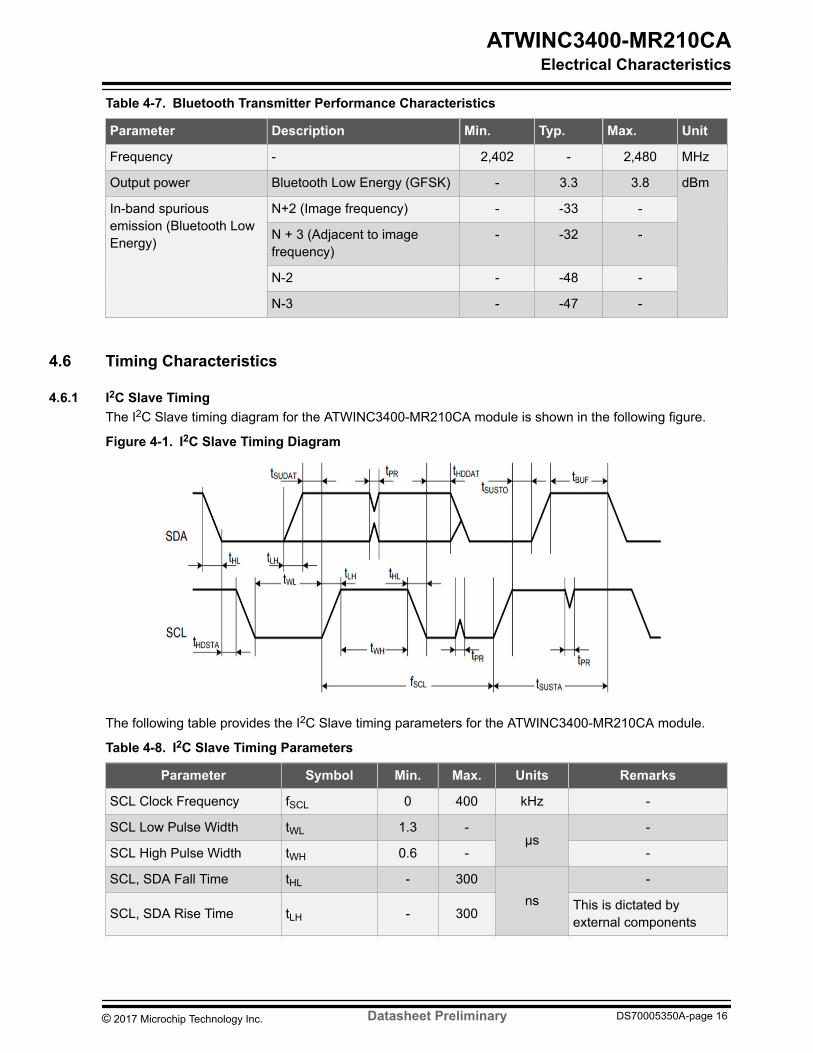
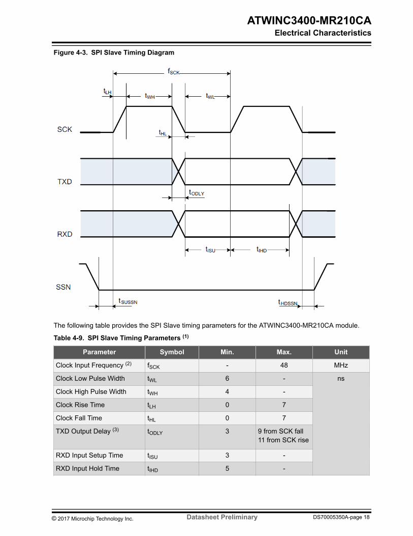

Parameter Symbol Min Max Unit
SSN Input Setup Time tSUSSN 5 -
SSN Input Hold Time tHDSSN 5 -
Note 1 Timing is applicable to all SPI modes2 Maximum clock frequency specified is limited by the SPI Slave interface internal design actual
maximum clock frequency can be lower and depends on the specific PCB layout3 Timing based on 15 pF output loading
463 SPI Master TimingThe SPI Master timing for the ATWINC3400-MR210CA module is shown in the following figureFigure 4-4 SPI Master Timing Diagram
The following table provides the SPI Master timing parameters for the ATWINC3400-MR210CA module
Table 4-10 SPI Master Timing Parameters (1)
Parameter Symbol Min Max Unit
Clock Output Frequency (2) fSCK - 20 MHz
Clock Low Pulse Width tWL 19 - ns
Clock High Pulse Width tWH 21 -
Clock Rise Time (3) tLH - 11
Clock Fall Time (3) tHL - 10
RXD Input Setup Time tISU 24 -
RXD Input Hold Time tIHD 0 -
SSNTXD Output Delay (3) tODLY -5 3
ATWINC3400-MR210CAElectrical Characteristics
copy 2017 Microchip Technology Inc Datasheet Preliminary DS70005350A-page 19
Note 1 Timing is applicable to all SPI modes2 Maximum clock frequency specified is limited by the SPI Master interface internal design actual
maximum clock frequency can be lower and depends on the specific PCB layout3 Timing based on 15 pF output loading
ATWINC3400-MR210CAElectrical Characteristics
copy 2017 Microchip Technology Inc Datasheet Preliminary DS70005350A-page 20
5 Power Management
51 Device StatesThe ATWINC3400-MR210CA module has multiple device states based on the state of the IEEE 80211and Bluetooth subsystems It is possible for both subsystems to be active at the same time To simplifythe device power consumption breakdown the following basic states are defined One subsystem can beactive at a time
bull WiFi_ON_Transmit ndash Device actively transmits IEEE 80211 signalbull WiFi_ON_Receive ndash Device actively receives IEEE 80211 signalbull BT_ON_Transmit ndash Device actively transmits Bluetooth signalbull BT_ON_Receive ndash Device actively receives Bluetooth signalbull Doze ndash Device is powered on but it does not actively transmit or receive databull Power_Down ndash Device core supply is powered off
52 Controlling Device StatesThe following table shows different device states and its power consumption The device states can beswitched using the following
bull CHIP_EN ndash Module pin (pin 19) enables or disables the DCDC converterbull VDDIO ndash IO supply voltage from external supply
In the ON states VDDIO is ON and CHIP_EN is high (at VDDIO voltage level) To change from the ONstates to Power_Down state connect the RESETN and CHIP_EN pin to logic low (GND) by following thepower-down sequence mentioned in Figure 5-1 When VDDIO is OFF and CHIP_EN is low the chip ispowered off with no leakage
Table 5-1 ATWINC3400-MR210CA Device States Current Consumption
Device State Code Rate Output Power(dBm)
Current Consumption(1)
IVBAT IVDDIO
ON_WiFi_Transmit 80211b 1 Mbps 167 271 mA 24 mA
80211b 11 Mbps 175 265 mA 24 mA
80211g 6 Mbps 183 275 mA 24 mA
80211g 54 Mbps 130 235 mA 24 mA
80211n MCS 0 175 272 mA 24 mA
80211n MCS 7 125 232 mA 24 mA
ON_WiFi_Receive 80211b 1 Mbps NA 639 mA 237 mA
80211b 11 Mbps NA 639 mA 237 mA
80211g 6 Mbps NA 639 mA 237 mA
80211g 54 Mbps NA 639 mA 237 mA
ATWINC3400-MR210CAPower Management
copy 2017 Microchip Technology Inc Datasheet Preliminary DS70005350A-page 21
Device State Code Rate Output Power(dBm)
Current Consumption(1)
IVBAT IVDDIO
80211n MCS 0 NA 639 mA 237 mA
80211n MCS 7 NA 639 mA 237 mA
ON_BT_Transmit BLE 40 1 Mbps 33 7937 mA 2368 mA
ON_BT_Receive BLE 40 1 Mbps NA 5136 mA 2368 mA
Doze (Bluetooth LowEnergy Idle)
NA NA 53 mA (2)
Doze (Bluetooth LowEnergy Low Power)
NA NA 1 mA (2)
Power_Down NA NA 105 uA(2)
Note 1 Conditions VBAT = 33V VDDIO = 33V at 25degC2 Current consumption mentioned for these states is the sum of current consumed in VDDIO and
VBAT voltage rails
When power is not supplied to the device (DCDC converter output and VDDIO are OFF at groundpotential) voltage cannot be applied to the ATWINC3400-MR210CA module pins because each pincontains an ESD diode from the pin to supply This diode turns on when voltage higher than one diode-drop is supplied to the pin
If voltage must be applied to the signal pads when the chip is in a low-power state the VDDIO supplymust be ON so the Power_Down state must be used Similarly to prevent the pin-to-ground diode fromturning ON do not apply voltage that is more than one diode-drop below the ground to any pin
53 Power-UpDown SequenceThe following figure illustrates the power-updown sequence for the ATWINC3400-MR210CA module
Figure 5-1 Power-UpDown Sequence
tC
tB
tAVBATT
VDDIO
CHIP_EN
RESETN
XO Clock
tC
tB
tA
The following table provides power-updown sequence timing parameters
ATWINC3400-MR210CAPower Management
copy 2017 Microchip Technology Inc Datasheet Preliminary DS70005350A-page 22
Table 5-2 Power-UpDown Sequence Timing
Parameter Min Max Unit
s Description Notes
tA 0 - ms VBAT rise toVDDIO rise
VBAT and VDDIO can rise simultaneously orconnected together VDDIO must not rise beforeVBAT
tB 0 - ms VDDIO rise toCHIP_EN rise
CHIP_EN must not rise before VDDIO CHIP_ENmust be driven high or low and must not be leftfloating
tC 5 - ms CHIP_EN rise toRESETN rise
This delay is required to stabilize the XO clockbefore RESETN removal RESETN must be drivenhigh or low and must not be left floating
tArsquo 0 - ms VDDIO fall toVBAT fall
VBAT and VDDIO fall simultaneously or connectedtogether VBAT must not fall before VDDIO
tBrsquo 0 - ms CHIP_EN fall toVDDIO fall
VDDIO must not fall before CHIP_EN CHIP_ENand RESETN must fall simultaneously
tCrsquo 0 - ms RESETN fall toVDDIO fall
VDDIO must not fall before RESETN RESETNand CHIP_EN fall simultaneously
54 Digital IO Pin Behavior During Power-Up SequencesThe following table represents the digital IO pin states corresponding to the device power modes
Table 5-3 Digital IO Pin Behavior in Different Device States
Device State VDDIO CHIP_EN
RESETN Output Driver Input
Driver
Pull UpDownResistor (96
kOhm)
Power_Down core supplyOFF
High Low Low Disabled (Hi-Z) Disabled Disabled
Power-On Reset coresupply and hard reset ON
High High Low Disabled (Hi-Z) Disabled Enabled
Power-On Default coresupply ON device out ofreset and not programmed
High High High Disabled (Hi-Z) Enabled Enabled
On_Doze On_TransmitOn_Receive core supplyON device programmed byfirmware
High High High Programmedby firmware foreach pinenabled ordisabled
OppositeofOutputDriverstate
Programmed byfirmware foreach pinenabled ordisabled
ATWINC3400-MR210CAPower Management
copy 2017 Microchip Technology Inc Datasheet Preliminary DS70005350A-page 23
6 Clocking
61 Low-Power ClockThe ATWINC3400-MR210CA module requires an external 32768 kHz clock to be supplied at the modulepin 20 This clock is used during the sleep operation The frequency accuracy of this external clock mustbe within plusmn200 ppm
ATWINC3400-MR210CAClocking
copy 2017 Microchip Technology Inc Datasheet Preliminary DS70005350A-page 24
7 CPU and Memory Subsystem
71 ProcessorThe ATWINC3400-MR210CA module has two Cortus APS3 32-bit processors one is used for Wi-Fi andthe other is used for Bluetooth In IEEE 80211 mode the processor performs many of the MAC functionsincluding but not limited to association authentication power management security key managementand MSDU aggregationde-aggregation In addition the processor provides flexibility for various modes ofoperation such as Station (STA) and Access Point (AP) modes In Bluetooth mode the processorhandles multiple tasks of the Bluetooth protocol stack
72 Memory SubsystemThe APS3 core uses a 256 KB instructionboot ROM (160 KB for IEEE 80211 and 96 KB for Bluetooth)along with a 420 KB instruction RAM (128 KB for IEEE 80211 and 292 KB for Bluetooth) and a 128 KBdata RAM (64 KB for IEEE 80211 and 64 KB for Bluetooth) In addition the device uses a 160 KBsharedexchange RAM (128 KB for IEEE 80211 and 32 KB for Bluetooth) accessible by the processorand MAC which allows the processor to perform various data management tasks on the Tx and Rx datapackets
73 Nonvolatile MemoryThe ATWINC3400-MR210CA module has 768 bits of nonvolatile eFuse memory that can be read by theCPU after device reset This nonvolatile One-Time-Programmable (OTP) memory can be used to storecustomer-specific parameters such as the 80211 MAC address and Bluetooth address and variouscalibration information such as Tx power crystal frequency offset and other software-specificconfiguration parameters The eFuse is partitioned into six 128-bit banks The bit map of the first and lastbanks is shown in the following figure The purpose of the first 80 bits in bank 0 and the first 56 bits inbank 5 is fixed and the remaining bits are general-purpose software dependent bits reserved for futureuse Currently the Bluetooth address is derived from the Wi-Fi MAC address (BT_ADDR=MAC_ADDR+1) This eliminates the need to program the first 56 bits in bank 5 Since each bank and each bit can beprogrammed independently this allows for several updates of the device parameters following the initialprogramming For example if the MAC address has to be changed Bank 1 has to be programmed withthe new MAC address along with the values of Tx gain correction and frequency offset if they are usedand programmed in the Bank 0 The contents of Bank 0 have to be invalidated in this case byprogramming the Invalid bit in the Bank 0 This will allow the firmware to use the MAC address from Bank1
By default ATWINC3400-MR210CA modules are programmed with the MAC address and the frequencyoffset bits of Bank 0
ATWINC3400-MR210CACPU and Memory Subsystem
copy 2017 Microchip Technology Inc Datasheet Preliminary DS70005350A-page 25
Figure 7-1 ATWINC3400-MR210CA eFuse Bit Map
ATWINC3400-MR210CACPU and Memory Subsystem
copy 2017 Microchip Technology Inc Datasheet Preliminary DS70005350A-page 26
8 WLAN SubsystemThe WLAN subsystem is composed of the Media Access Controller (MAC) Physical Layer (PHY) andthe radio
81 MACThe ATWINC3400-MR210CA module is designed to operate at low power while providing high datathroughput The IEEE 80211 MAC functions are implemented with a combination of dedicated datapathengines hardwired control logic and a low power high-efficiency microprocessor The combination ofdedicated logic with a programmable processor provides optimal power efficiency and real time responsewhile providing the flexibility to accommodate evolving standards and future feature enhancements
The dedicated datapath engines are used to implement datapath functions with heavy computationalrequirements For example a Frame Check Sequence (FCS) engine checks the Cyclic RedundancyCheck (CRC) of the transmitting and receiving packets and a cipher engine performs all the requiredencryption and decryption operations for the WEP WPA-TKIP and WPA2 CCMP-AES securityrequirements
Control functions which have real time requirements are implemented using hardwired control logicmodules These logic modules offer real time response while maintaining configurability through theprocessor Examples of hardwired control logic modules are the channel access control module(implements EDCAHCCA Beacon Tx control interframe spacing and so on) protocol timer module(responsible for the Network Access vector back-off timing timing synchronization function and slotmanagement) MAC Protocol Data Unit (MPDU) handling module aggregationdeaggregation moduleblock ACK controller (implements the protocol requirements for burst block communication) and TxRxcontrol Finite State Machine (FSM) (coordinates data movement between PHY and MAC interface cipherengine and the Direct Memory Access (DMA) interface to the TxRx FIFOs)
The following are the characteristics of MAC functions implemented solely in software on themicroprocessor
bull Functions with high memory requirements or complex data structures Examples includeassociation table management and power save queuing
bull Functions with low computational load or without critical real time requirements Examples includeauthentication and association
bull Functions that require flexibility and upgradeability Examples include beacon frame processing andQoS scheduling
FeaturesThe ATWINC3400-MR210CA MAC supports the following functions
bull IEEE 80211bgnbull IEEE 80211e WMM QoS EDCAHCCAPCF multiple access categories traffic schedulingbull Advanced IEEE 80211n features
ndash Transmission and reception of aggregated MPDUs (A-MPDU)ndash Transmission and reception of aggregated MSDUs (A-MSDU)ndash Immediate block acknowledgmentndash Reduced Interframe Spacing (RIFS)
bull IEEE 80211i and WFA security with key management
ATWINC3400-MR210CAWLAN Subsystem
copy 2017 Microchip Technology Inc Datasheet Preliminary DS70005350A-page 27
ndash WEP 64128ndash WPA-TKIPndash 128-bit WPA2 CCMP (AES)
bull Advanced power managementndash Standard IEEE 80211 power save mode
bull RTS-CTS and CTS-self supportbull Either STA or AP mode in the infrastructure basic service set mode
82 PHYThe ATWINC3400-MR210CA module WLAN PHY is designed to achieve reliable and power-efficientphysical layer communication specified by IEEE 80211 bgn in single stream mode with 20 MHzbandwidth The advanced algorithms are used to achieve maximum throughput in a real worldcommunication environment with impairments and interference The PHY implements all the requiredfunctions such as Fast Fourier Transform (FFT) filtering Forward Error Correction (FEC) that is a Viterbidecoder frequency timing acquisition and tracking channel estimation and equalization carrier sensingclear channel assessment and automatic gain control
Features
The IEEE 80211 PHY supports the following functions
bull Single antenna 1x1 stream in 20 MHz channelsbull Supports IEEE 80211b DSSS-CCK modulation 1 2 55 and 11 Mbpsbull Supports IEEE 80211g OFDM modulation 6 9 1218 24 36 48 and 54 Mbpsbull Supports IEEE 80211n HT modulations MCS0-7 20 MHz 800 and 400ns guard interval 65 72
130 144 195 217 260 289 390 433 520 578 585 650 and 722 Mbpsbull IEEE 80211n mixed mode operationbull Per packet Tx power controlbull Advanced channel estimationequalization automatic gain control CCA carriersymbol recovery
and frame detection
83 RadioThis section presents information describing the properties and characteristics of the ATWINC3400-MR210CA and Wi-Fi radio transmit and receive performance capabilities of the device
The performance measurements are taken at the RF pin assuming 50Ω impedance the RF performanceis guaranteed for room temperature of 25oC with a derating of 2-3 dB at boundary conditions
Measurements were taken under typical conditions VBATT=33V VDDIO=33V temperature +25ordmC
Table 8-1 Features and Properties
Feature Description
Part Number ATWINC3400-MR210CA
WLAN Standard IEEE 80211 bgn Wi-Fi compliant
Host Interface SPI
ATWINC3400-MR210CAWLAN Subsystem
copy 2017 Microchip Technology Inc Datasheet Preliminary DS70005350A-page 28
Feature Description
Dimension 224 x 147 x 20 mm
Frequency Range 2412GHz ~ 2472GHz (24GHz ISM Band)
Number of Channels 11 for North America and 13 for Europe and Japan
Modulation 80211b DQPSK DBPSK CCK80211gn OFDM 64-QAM16-QAM QPSK BPSK
Data Rate 80211b 1 2 55 11Mbps
80211g 6 9 12 18 24 36 48 54Mbps
Data Rate(20 MHz normal GI 800 ns)
80211n 65 13 195 26 39 52 585 65Mbps
Data Rate(20 MHz short GI 400 ns)
80211n 72 144 217 289 433 57865722Mbps
Operating temperature -40 to +85oC
ATWINC3400-MR210CAWLAN Subsystem
copy 2017 Microchip Technology Inc Datasheet Preliminary DS70005350A-page 29
9 Bluetooth Low Energy 40The Bluetooth subsystem implements all the mission critical real-time functions It encodesdecodes HCIpackets constructs baseband data packages and manages and monitors the connection status slotusage data flow routing segmentation and buffer control The Bluetooth subsystem supports BluetoothLow Energy modes of operation
Supports the following advanced low energy applications
bull Smart energybull Consumer wellnessbull Home automationbull Securitybull Proximity detectionbull Entertainmentbull Sports and Fitnessbull Automotive
Coexistence MechanismThe ATWINC3400 supports simultaneous usage of both Bluetooth Low Energy and Wi-Fi via acoexistence mechanism that allows the protocols to share the same radio The radio defaults to Wi-Fiusage until a Bluetooth Low Energy event occurs (such as connection or advertising) in which case theradio is gracefully switched over for Bluetooth Low Energy use For the duration of the Bluetooth LowEnergy event the radio is switched back and forth between Wi-Fi and Bluetooth Low Energy asdemanded by the Bluetooth Low Energy activity before returning to Wi-Fi until the next Bluetooth LowEnergy event
ATWINC3400-MR210CABluetooth Low Energy 40
copy 2017 Microchip Technology Inc Datasheet Preliminary DS70005350A-page 30
10 External Interfaces
101 Interfacing with the Host MicrocontrollerThis section describes interfacing the ATWINC3400-MR210CA module with the host microcontroller Theinterface is comprised of a slave SPI and additional control signals as shown in the following figure Formore information on SPI interface specification and timing refer to the SPI Interface Additional controlsignals are connected to the GPIOIRQ interface of the microcontroller
Figure 10-1 Interfacing with Host Microcontroller
Host Microcontroller
CHIP_EN
RESET
WAKE
IRQN
SPI Wi-Fi Controller
Module
Table 10-1 Host Microcontroller Interface Pins
Pin Number Function
4 RESET_N
11 WAKE
13 IRQ_N
22 CHIP_EN
16 SPI_SSN
15 SPI_MOSI
17 SPI_MISO
18 SPI_SCK
Related LinksSPI Interface
ATWINC3400-MR210CAExternal Interfaces
copy 2017 Microchip Technology Inc Datasheet Preliminary DS70005350A-page 31
102 SPI Interface
1021 OverviewThe ATWINC3400-MR210CA has a Serial Peripheral Interface (SPI) that operates as an SPI slave TheSPI interface can be used for control and for serial IO of 80211 data The SPI pins are mapped asshown in the following table The SPI is a full-duplex slave-synchronous serial interface that is availableimmediately following reset when pin 10 (SPI_CFG) is tied to VDDIO
Table 10-2 SPI Interface Pin Mapping
Pin SPI function
10 CFG Must be tied to VDDIO
16 SSN Active-Low Slave Select
15 MOSI(RXD) Serial Data Receive
18 SCK Serial Clock
17 MISO(TXD) Serial Data Transmit
When the SPI is not selected that is when SSN is high the SPI interface will not interfere with datatransfers between the serial-master and other serial-slave devices When the serial slave is not selectedits transmitted data output is buffered resulting in a high impedance drive onto the MISO line
The SPI interface responds to a protocol that allows an external host to read or write any register in thechip as well as initiate DMA transfers
The SPI SSN MOSI MISO and SCK pins of the ATWINC3400-MR210CA have internal programmablepull-up resistors These resistors should be programmed to be disabled otherwise if any of the SPI pinsare driven to a low level while the ATWINC3400-MR210CA is in the low power sleep state the current willflow from the VDDIO supply through the pull-up resistors increasing the current consumption of themodule
1022 SPI TimingThe SPI Slave interface supports four standard modes as determined by the Clock Polarity (CPOL) andClock Phase (CPHA) settings These modes are illustrated in the following table and figure
Table 10-3 SPI Slave Modes
Mode CPOL CPHA
0 0 0
1 0 1
2 1 0
3 1 1
The red lines in the following figure correspond to Clock Phase = 0 and the blue lines correspond to ClockPhase = 1
ATWINC3400-MR210CAExternal Interfaces
copy 2017 Microchip Technology Inc Datasheet Preliminary DS70005350A-page 32
Figure 10-2 SPI Slave Clock Polarity and Clock Phase Timing
z
z z
z
SCKCPOL = 0
CPOL = 1
SSN
RXDTXD(MOSIMISO)
CPHA = 0
CPHA = 1
2 3 4 5 6 7 8
1 2 3 4 5 6 7
1
8
The SPI timing is provided in the following figure and table
Figure 10-3 SPI Timing Diagram (SPI Mode CPOL=0 CPHA=0)
t LH
SCK
TXD
RXD
t WH
t HL
t WL
t ODLY
t ISU t IHD
f SCK
SSN
t SUSSN t HDSSN
Table 10-4 SPI Slave Timing Parameters1
Parameter Symbol Min Max Units
Clock Input Frequency2 fSCK mdash 48 MHz
Clock Low Pulse Width tWL 4 mdash
nsClock High Pulse Width tWH 5 mdash
Clock Rise Time tLH 0 7
Clock Fall Time tHL 0 7
ATWINC3400-MR210CAExternal Interfaces
copy 2017 Microchip Technology Inc Datasheet Preliminary DS70005350A-page 33
Parameter Symbol Min Max Units
TXD Output Delay3 tODLY 4 9 from SCK fall125 from SCKrise
RXD Input Setup Time tISU 1 mdash
RXD Input Hold Time tIHD 5 mdash
SSN Input Setup Time tSUSSN 3 mdash
SSN Input Hold Time tHDSSN 55 mdash
Note 1 Timing is applicable to all SPI modes2 Maximum clock frequency specified is limited by the SPI Slave interface internal design actual
maximum clock frequency can be lower and depends on the specific PCB layout3 Timing based on 15pF output loading
103 UART InterfaceThe ATWINC3400-MR210CA supports the Universal Asynchronous ReceiverTransmitter (UART)interface This interface should be used for debug purposes only The two UART pins TXDRXD areavailable on pin J16 and pin J17 respectively The UART is compatible with the RS-232 standard
The default configuration for accessing the UART interface of ATWINC3400-MR210CA is mentionedbelow
bull Baud rate 460800bull Data 8 bitbull Parity Nonebull Stop bit 1 bitbull Flow control None
It also has RX and TX FIFOs which ensure reliable high-speed reception and low software overheadtransmission FIFO size is 4 x 8 for both RX and TX direction The UART also has status registersshowing the number of received characters available in the FIFO and various error conditions as well theability to generate interrupts based on these status bits
An example of the UART receiving or transmitting a single packet is shown in the following figure Thisexample shows 7-bit data (0x45) odd parity and two stop bits
Important UART2 supports RTS and CTS flow control The UART RTS and UART CTSMUST be connected to the host MCU UART and enabled for the UART interface to befunctional
ATWINC3400-MR210CAExternal Interfaces
copy 2017 Microchip Technology Inc Datasheet Preliminary DS70005350A-page 34
Figure 10-4 Example of UART RX of TX Packet
Previous Packets or
Leading Idle Bits
Current Packet
DataStart Bit
Parity Bit Stop Bits
Next Packet
ATWINC3400-MR210CAExternal Interfaces
copy 2017 Microchip Technology Inc Datasheet Preliminary DS70005350A-page 35
11 Application Reference DesignThe ATWINC3400-MR210CA module application schematics for different supported host interfaces areshown in this section
111 Host Interface - SPIFigure 11-1 ATWINC3400-MR210CA Reference Schematic
R5 0
R90
R3 0
R20
R8 0
TP2
R100
U1
ATWINC3400-MR210
I2C_SCL_M J34I2C_SDA_M J35
RESETN J7
NC
1 J3
NC
2 J4
NC
3 J5
NC
4 J6
GN
D5
J36
SDIO~_SPI_CFG J2
GN
D1
J1IRQN
J33
UART_TxD J16
SPI_MOSI J26
SPI_SSN J25
SPI_MISO J24
SPI_SCK J23
UART_RxD J17
VB
AT
J1
8
CHIP_EN J19
VD
DIO
J1
2
GPIO3 J14GPIO4 J15
GN
D3
J22
GN
D4
J28
BT_TXD J8
BT_RXD J9
BT_RTS J10
BT_CTS J11
GPIO17 J29GPIO18 J30GPIO19 J31
GN
D2
J13
GPIO7 J27
GPIO20 J32
GN
D_P
AD
J4
9
RT
C
J20
R6 0
R1 1M
R4 0
R7 0
TP1
SPI_SSNSPI_MISOSPI_SCK
SPI_MOSI
Reset_N
Chip_EN
UART_TxDUART_RxD
GPIO_17
IRQN
VBAT
GPIO_4GPIO_7
VDDIOVDDIO
To host UART output To host UART input
(General Purpose IO)
To host SPI Master
Resistors R2 - R14 are recomm ended as placeholders in case filtering of noisy s ignals is required They also allow disconnecting of module for debug purposes
GPIO_3
GPIO_19GPIO_20
GPIO_18
(To host GPIO)
(To host GPIO)
R12 0R11 0BT_RTS
BT_CTSTo Host Input To Host Output
BT_TxDBT_RxD
To Host Input To Host Output R14 0
R13 0
C1
01uF
U2
32768KHz
OE
3
VS
S
2
O 1V
DD
4
VDDIO
Note It is recommended to add test points for module pins J8 J9 J10 J11 J16 and J17 in the design
The following table provides the reference Bill of Material (BoM) details for the ATWINC3400-MR210CAmodule with SPI as host interface
Table 11-1 ATWINC3400-MR210CA Reference Bill of Materials for SPI Operation
Item Quantity Reference
Value Description Manufacturer PartNumber
Footprint
1 1 U1 ATWINC3400-MR210CA
Wi-FiBluetoothBLE
MicrochipTechnologyIncreg
ATWINC3400-MR210CA
Custom
ATWINC3400-MR210CAApplication Reference Design
copy 2017 Microchip Technology Inc Datasheet Preliminary DS70005350A-page 36
Item Quantity Reference
Value Description Manufacturer PartNumber
Footprint
ComboModule
2 1 U2 ASH7KW-32768kHZ-L-T
Oscillator32768 kHz+0-175 ppm12V - 55V-40degC - +85degC
Abraconreg
CorporationASH7KW-32768kHZ-L-T
OSCCC320X150X100-4N
3 1 R1 1M RESISTORThick Film 1MOhm 0201
Panasonicreg ERJ-1GEJ105C
RS0201
4 13 R2-R14 0 RESISTORThick Film 0Ohm 0201
Panasonicreg ERJ-1GN0R00C
RS0201
ATWINC3400-MR210CAApplication Reference Design
copy 2017 Microchip Technology Inc Datasheet Preliminary DS70005350A-page 37
12 Module Outline DrawingsThe ATWINC3400-MR210CA module package details are outlined in the following figureFigure 12-1 ATWINC3400-MR210CA Footprint and Module Package Drawings - Top Bottom andSide View
ATWINC3400-MR210CA
ATWINC3400-MR210CAUntoleranced dimensions
Note 1 Dimensions are in mm2 It is recommended to have a 5x5 grid of GND vias solidly connecting the exposed GND paddle of
the module to the ground plane on the innerother layers of the host board This will provide a goodground and thermal transfer for the ATWINC3400-MR210CA module
ATWINC3400-MR210CAModule Outline Drawings
copy 2017 Microchip Technology Inc Datasheet Preliminary DS70005350A-page 38
13 Design ConsiderationThis section provides the guidelines on module placement and routing to achieve the best performance
131 Module Placement and Routing GuidelinesIt is critical to follow the recommendations listed below to achieve the best RF performance
bull The module must be placed on the host board and the chip antenna area must not overlap with thehost board The following figure on placement reference shows the best poor and worst casemodule placements in the host boardFigure 13-1 ATWINC3400-MR210CA Placement Example
CAUTION Caution Do not place the module in the middle of the host board or far away from thehost board edge
bull Follow the host board mechanical recommendation ground plane and keep out recommendationsas shown in the following figure Module chip antenna is specifically tuned for this host boardmechanical recommendation as shown in the following figure The host PCB should have athickness of 15 mm
ndash Follow the module placement and keep out recommendation as shown in the following figurebull Avoid routing any traces on the top layer of the host board which will be directly below
the module areabull In the keep out region there should be no copper traces in all signal layersbull Avoid placing any components (like mechanical spacers bumpon and so on) on the
host board closer to the chip antenna region
ATWINC3400-MR210CADesign Consideration
copy 2017 Microchip Technology Inc Datasheet Preliminary DS70005350A-page 39
bull Place the GND polygon pour below the module on the top layer of the host board Avoidbreaks in this GND plane and ensure continuous GND plane for better RF performance
bull GND polygon pour in the top layer of the host board should have a minimum area of 20x 40 mm
bull Place sufficient GND vias on host board edge and below the module for better RFperformance
bull It is recommended to have a 5x5 grid of GND vias solidly connecting the exposed GNDpaddle of the module to the ground plane of the host board This will act as a goodground and thermal conduction path for the ATWINC3400-MR210CA module The GNDvias should have a minimum via hole size of 02 mm
bull Antenna on the module should not be placed in direct contact or close proximity toplastic casingobjects Keep a minimum clearance of gt7 mm in all directions around thechip antenna
Figure 13-2 ATWINC3400-MR210CA Placement Reference
132 Antenna PerformanceThe ATWINC3400-MR210CA uses a chip antenna which is fed via matching network The table belowlists the technical specification of the chip antennaTable 13-1 Chip antenna specification
Paramater Value
Peak gain 05 dBi
Operating frequency 2400 - 2500 MHz
ATWINC3400-MR210CADesign Consideration
copy 2017 Microchip Technology Inc Datasheet Preliminary DS70005350A-page 40
Paramater Value
Antenna PN 2450AT18A100
Antenna vendor Johanson Technology
ATWINC3400-MR210CADesign Consideration
copy 2017 Microchip Technology Inc Datasheet Preliminary DS70005350A-page 41
14 Reflow Profile InformationThis section provides the guidelines for the reflow process to get the module soldered to the customersdesign
141 Storage Condition
1411 Moisture Barrier Bag Before OpeningA moisture barrier bag must be stored at a temperature of less than 30degC with humidity under 85 RH
The calculated shelf life for the dry-packed product is 12 months from the date the bag is sealed
1412 Moisture Barrier Bag OpenHumidity indicator cards must be blue lt 30
142 Solder PasteThe SnAgCu eutectic solder with melting temperature of 217degC is most commonly used for lead-freesolder reflow application This alloy is widely accepted in the semiconductor industry due to its low costrelatively low melting temperature and good thermal fatigue resistance Some recommended pastesinclude NC-SMQreg 230 flux and Indalloyreg 241 solder paste made up of 955 Sn38 Ag07 Cu or SENJUN705-GRN3360-K2-V Type 3 no clean paste
143 Stencil DesignThe recommended stencil is laser-cut stainless-steel type with thickness of 100 microm to 130 microm andapproximately a 11 ratio of stencil opening to pad dimension To improve paste release a positive taperwith bottom opening 25 microm larger than the top is utilized Local manufacturing experience may find othercombinations of stencil thickness and aperture size to get good results
144 Baking ConditionsThis module is rated at MSL level 3 After the sealed bag is opened no baking is required within 168hours as long as the devices are held at le 30degC60 RH or stored at lt 10 RH
The module requires baking before mounting ifbull The sealed bag has been open for more than 168 hoursbull The humidity indicator card reads more than 10bull SIPs need to be baked for eight hours at 125degC
145 Soldering and Reflow ConditionOptimization of the reflow process is the most critical factor considered for lead-free soldering Thedevelopment of an optimal profile must account the paste characteristics the size of the board thedensity of the components the mix of the larger and smaller components and the peak temperaturerequirements of the components An optimized reflow process is the key to ensuring a successful lead-free assembly and achieves high yield and long-term solder joint reliability
ATWINC3400-MR210CAReflow Profile Information
copy 2017 Microchip Technology Inc Datasheet Preliminary DS70005350A-page 42
Temperature ProfilingTemperature profiling must be performed for all new board designs by attaching thermocouples at thesolder joints on the top surface of the larger components and at multiple locations of the boards This isto ensure that all components are heated to a temperature above the minimum reflow temperatures andthe smaller components do not exceed the maximum temperature limit The SnAgCu solder alloy melts at~217degC so the reflow temperature peak at joint level must be 15 to 20degC higher than meltingtemperature The targeted solder joint temperature for the SnAgCu solder must be ~235degC For larger orsophisticated boards with a large mix of components it is also important to ensure that the temperaturedifference across the board is less than 10 degrees to minimize board warpage The maximumtemperature at the component body must not exceed the MSL3 qualification specification
1451 Reflow OvenIt is strongly recommended that a reflow oven equipped with more heating zones and Nitrogenatmosphere must be used for the lead-free assembly The Nitrogen atmosphere is shown to improve thewet-ability and reduce temperature gradient across the board It can also enhance the appearance of thesolder joints by reducing the effects of oxidation
The following items must also be observed in the reflow process1 Some recommended pastes include
ndash NC-SMQreg 230 flux and Indalloyreg 241 solder paste made up of 955 Sn38 Ag07 Cundash SENJU N705-GRN3360-K2-V Type 3 no clean paste
2 Allowable reflow soldering iterationsndash Three times based on the following reflow soldering profile (see following figure)
3 Temperature profilendash Reflow soldering must be done according to the following temperature profile (see following
figure)ndash Peak temperature 250degC
ATWINC3400-MR210CAReflow Profile Information
copy 2017 Microchip Technology Inc Datasheet Preliminary DS70005350A-page 43
Figure 14-1 Solder Reflow Profile
CleaningThe exposed ground paddle helps to self-align the module avoiding pad misalignment The use of noclean solder pastes is recommended As a result of the reflow process be sure to completely dry the no-clean paste fluxes This may require longer reflow profiles andor peak temperatures toward the high endof the process window as recommended by the solder paste vendor It is believed that uncured fluxresidues can lead to corrosion andor shorting in accelerated testing and possibly the field
ReworkThe rework removes the mounted SIP package and replaces it with a new unit It is recommended thatonce an ATWINC3400-MR210CA module is removed and it must never be reused During the reworkprocess the mounted module and PCB are heated partially and the module is removed It isrecommended to heat-proof the proximity of the mounted parts and junctions and use the best nozzle forrework that is suited to the module size
ATWINC3400-MR210CAReflow Profile Information
copy 2017 Microchip Technology Inc Datasheet Preliminary DS70005350A-page 44
15 Module Assembly ConsiderationsThe ATWINC3400-MR210CA module is assembled with an EMI shield to ensure compliance with EMIemission and immunity rules The EMI shield is made of a tin-plated steel (SPTE) and is not hermeticallysealed Solutions such as IPA and similar solvents can be used to clean this module Cleaning solutionscontaining acid must never be used on the module
The ATWINC3400-MR210CA module is manufactured without any conformal coating applied It is thecustomers responsibility if a conformal coating is specified andor applied to this module
ATWINC3400-MR210CAModule Assembly Considerations
copy 2017 Microchip Technology Inc Datasheet Preliminary DS70005350A-page 45
16 Regulatory ApprovalRegulatory Approvals received for ATWINC3400-MR210CA
bull United StatesFCC ID 2ADHKWINC3400bull CanadaISED
ndash IC 20266-ATWINC3400ndash HVIN ATWINC3400-MR210CA
bull Europe - CE
161 United StatesThe ATWINC3400-MR210CA module has received Federal Communications Commission (FCC) CFR47Telecommunications Part 15 Subpart C ldquoIntentional Radiatorsrdquo single-modular approval in accordancewith Part 15212 Modular Transmitter approval Single-modular transmitter approval is defined as acomplete RF transmission sub-assembly designed to be incorporated into another device that mustdemonstrate compliance with FCC rules and policies independent of any host A transmitter with amodular grant can be installed in different end-use products (referred to as a host host product or hostdevice) by the grantee or other equipment manufacturer then the host product may not require additionaltesting or equipment authorization for the transmitter function provided by that specific module or limitedmodule device
The user must comply with all of the instructions provided by the Grantee which indicate installationandor operating conditions necessary for compliance
A host product itself is required to comply with all other applicable FCC equipment authorizationregulations requirements and equipment functions that are not associated with the transmitter moduleportion For example compliance must be demonstrated to regulations for other transmitter componentswithin a host product to requirements for unintentional radiators (Part 15 Subpart B) such as digitaldevices computer peripherals radio receivers etc and to additional authorization requirements for thenon-transmitter functions on the transmitter module (ie Verification or Declaration of Conformity) asappropriate (eg Bluetooth and Wi-Fi transmitter modules may also contain digital logic functions)
1611 Labeling And User Information RequirementsThe ATWINC3400-MR210CA module has been labeled with its own FCC ID number and if the FCC ID isnot visible when the module is installed inside another device then the outside of the finished product intowhich the module is installed must display a label referring to the enclosed module This exterior labelcan use wording as follows
For the ATWINC3400-MR210CA
Contains Transmitter Module FCC ID 2ADHKWINC3400
or
Contains FCC ID 2ADHKWINC3400
This device complies with Part 15 of the FCC Rules Operation is subject to the following twoconditions (1) this device may not cause harmful interference and (2) this device must acceptany interference received including interference that may cause undesired operation
A users manual for the finished product should include the following statement
ATWINC3400-MR210CARegulatory Approval
copy 2017 Microchip Technology Inc Datasheet Preliminary DS70005350A-page 46
This equipment has been tested and found to comply with the limits for a Class B digital devicepursuant to part 15 of the FCC Rules These limits are designed to provide reasonable protectionagainst harmful interference in a residential installation This equipment generates uses and can radiateradio frequency energy and if not installed and used in accordance with the instructions may causeharmful interference to radio communications However there is no guarantee that interference will notoccur in a particular installation If this equipment does cause harmful interference to radio or televisionreception which can be determined by turning the equipment off and on the user is encouraged to tryto correct the interference by one or more of the following measures
bull Reorient or relocate the receiving antennabull Increase the separation between the equipment and receiverbull Connect the equipment into an outlet on a circuit different from that to which the receiver is
connectedbull Consult the dealer or an experienced radioTV technician for help
Additional information on labeling and user information requirements for Part 15 devices can be found inKDB Publication 784748 which is available at the FCC Office of Engineering and Technology (OET)Laboratory Division Knowledge Database (KDB) httpsappsfccgovoetcfkdbindexcfm
1612 RF ExposureAll transmitters regulated by FCC must comply with RF exposure requirements KDB 447498 General RFExposure Guidance provides guidance in determining whether proposed or existing transmitting facilitiesoperations or devices comply with limits for human exposure to Radio Frequency (RF) fields adopted bythe Federal Communications Commission (FCC)
From the FCC Grant Output power listed is conducted This transmitter is restricted for use with thespecific antenna(s) tested in this application for Certification
The antenna(s) used with this transmitter must be installed to provide a separation distance of at least 65cm from all persons and must not be co-located or operating in conjunction with any other antenna ortransmitter Users and installers must be provided with antenna installation instructions and transmitteroperating conditions for satisfying RF exposure compliance
1613 Helpful Web SitesFederal Communications Commission (FCC) httpwwwfccgov
FCC Office of Engineering and Technology (OET) Laboratory Division Knowledge Database (KDB) httpsappsfccgovoetcfkdbindexcfm
162 CanadaThe ATWINC3400-MR210CA module has been certified for use in Canada under Innovation Science andEconomic Development Canada (ISED formerly Industry Canada) Radio Standards Procedure (RSP)RSP-100 Radio Standards Specification (RSS) RSS-Gen and RSS-247 Modular approval permits theinstallation of a module in a host device without the need to recertify the device
1621 Labeling and User Information RequirementsLabel Requirements (from RSP-100 Issue 11 Section 3) The host device shall be properly labeled toidentify the module within the host device
The Innovation Science and Economic Development Canada certification label of a module shall beclearly visible at all times when installed in the host device otherwise the host product must be labeled to
ATWINC3400-MR210CARegulatory Approval
copy 2017 Microchip Technology Inc Datasheet Preliminary DS70005350A-page 47
display the Innovation Science and Economic Development Canada certification number of the modulepreceded by the word ldquoContainsrdquo or similar wording expressing the same meaning as follows
For the ATWINC3400-MR210CA
Contains IC 20266-ATWINC3400
User Manual Notice for License-Exempt Radio Apparatus (from Section 84 RSS-Gen Issue 4November 2014) User manuals for license-exempt radio apparatus shall contain the following orequivalent notice in a conspicuous location in the user manual or alternatively on the device or both
This device complies with Industry Canada license exempt RSS standard(s) Operation issubject to the following two conditions
(1) This device may not cause interference and
(2) This device must accept any interference including interference that may cause undesiredoperation of the device
Le preacutesent appareil est conforme aux CNR dIndustrie Canada applicables aux appareils radioexempts de licence Lexploitation est autoriseacutee aux deux conditions suivantes
(1) lappareil ne doit pas produire de brouillage et
(2) lutilisateur de lappareil doit accepter tout brouillage radioeacutelectrique subi mecircme si lebrouillage est susceptible den compromettre le fonctionnement
Guidelines on Transmitter Antenna for License Exempt Radio Apparatus
Under Industry Canada regulations this radio transmitter may only operate using an antenna ofa type and maximum (or lesser) gain approved for the transmitter by Industry Canada To reducepotential radio interference to other users the antenna type and its gain should be so chosenthat the equivalent isotropically radiated power (eirp) is not more than that necessary forsuccessful communication
Conformeacutement agrave la reacuteglementation dIndustrie Canada le preacutesent eacutemetteur radio peutfonctionner avec une antenne dun type et dun gain maximal (ou infeacuterieur) approuveacute pourleacutemetteur par Industrie Canada Dans le but de reacuteduire les risques de brouillage radioeacutelectriqueagrave lintention des autres utilisateurs il faut choisir le type dantenne et son gain de sorte que lapuissance isotrope rayonneacutee eacutequivalente (pire) ne deacutepasse pas lintensiteacute neacutecessaire agraveleacutetablisse-ment dune communication satisfaisante
1622 RF ExposureAll transmitters regulated by Innovation Science and Economic Development Canada (ISED) mustcomply with RF exposure requirements listed in RSS-102 - Radio Frequency (RF) Exposure Complianceof Radio communication Apparatus (All Frequency Bands)
This transmitter is restricted for use with a specific antenna tested in this application for certification andmust not be co-located or operating in conjunction with any other antenna or transmitters within a hostdevice except in accordance with Canada multi-transmitter product procedures
The installation of the transmitter must ensure that the antenna has a separation distance of at least 65cm from all persons or compliance must be demonstrated according to the ISED SAR procedures
ATWINC3400-MR210CARegulatory Approval
copy 2017 Microchip Technology Inc Datasheet Preliminary DS70005350A-page 48
1623 Helpful Web SitesInnovation Science and Economic Development Canada httpwwwicgcca
163 EuropeThe ATWINC3400-MR210CA module is a Radio Equipment Directive (RED) assessed radio module thatis CE marked and has been manufactured and tested with the intention of being integrated into a finalproduct
The ATWINC3400-MR210CA module has been tested to RED 201453EU Essential Requirements forHealth and Safety (Article (31(a)) Electromagnetic Compatibility (EMC) (Article 31(b)) and Radio(Article 32) which is summarized in the following European Compliance Testing table
The ETSI provides guidance on modular devices in the ldquoGuide to the application of harmonised standardscovering articles 31b and 32 of the RED 201453EU (RED) to multi-radio and combined radio and non-radio equipmentrdquo document available at httpwwwetsiorgdeliveretsi_eg203300_203399203367010101_60eg_203367v010101ppdf
Note To maintain conformance to the testing listed in the following European Compliance Testing tablethe module shall be installed in accordance with the installation instructions in this data sheet and shallnot be modified When integrating a radio module into a completed product the integrator becomes themanufacturer of the final product and is therefore responsible for demonstrating compliance of the finalproduct with the essential requirements against the RED
1631 Labeling and User Information RequirementsThe label on the final product that contains the ATWINC3400-MR210CA module must follow CE markingrequirements
Table 16-1 European Compliance Testing
Certification Standards Article Laboratory
Report Number Date
Safety EN60950-12006A112009 A12010A122011A22013
[31(a)] TUVRheinlandTaiwan
10062655 001 31-Oct-2017
Health EN300328 V211EN624792010
50103733 001 31-Oct-2017
EN300328 V211EN623112008
50103734 001 31-Oct-2017
EMC EN301489-1 V211EN301489-1 V220
[31(b)] 10062417 001 31-Oct-2017
EN301489-17 V311
EN301489-17 V320
Radio EN300328 V211 [32] 50103733 00150103734 001
31-Oct-2017
ATWINC3400-MR210CARegulatory Approval
copy 2017 Microchip Technology Inc Datasheet Preliminary DS70005350A-page 49
1632 Conformity AssessmentFrom ETSI Guidance Note EG 203367 section 61 when non-radio products are combined with a radioproduct
If the manufacturer of the combined equipment installs the radio product in a host non-radio product inequivalent assessment conditions (ie host equivalent to the one used for the assessment of the radioproduct) and according to the installation instructions for the radio product then no additional assessmentof the combined equipment against article 32 of the RED is required
The European Compliance Testing listed in the preceeding table was performed using the integral chipantenna
16321 Simplified EU Declaration of ConformityHereby Microchip Technology Inc declares that the radio equipment type ATWINC3400-MR210CA is incompliance with Directive 201453EU
The full text of the EU declaration of conformity for this product is available at httpwwwmicrochipcomdesign-centerswireless-connectivity
1633 Helpful WebsitesA document that can be used as a starting point in understanding the use of Short Range Devices (SRD)in Europe is the European Radio Communications Committee (ERC) Recommendation 70-03 E whichcan be downloaded from the European Communications Committee (ECC) at httpwwwecodocdbdk
Additional helpful web sites are
bull Radio Equipment Directive (201453EU)httpseceuropaeugrowthsingle-marketeuropean-standardsharmonised-standardsred_en
bull European Conference of Postal and Telecommunications Administrations (CEPT)httpwwwceptorg
bull European Telecommunications Standards Institute (ETSI)httpwwwetsiorg
bull The Radio Equipment Directive Compliance Association (REDCA)httpwwwredcaeu
164 Other Regulatory Informationbull For information about other countries jurisdictions not covered here refer to http
wwwmicrochipcom design-centerswireless-connectivitybull Should other regulatory jurisdiction certification be required by the customer or the customer needs
to recertify the module for other reasons contact Microchip for the required utilities anddocumentation
ATWINC3400-MR210CARegulatory Approval
copy 2017 Microchip Technology Inc Datasheet Preliminary DS70005350A-page 50
17 Reference DocumentationThe following are the set of collaterals to ease integration and device ramp
bull Wi-Fi Network Controller Software Design Guide Application Notebull Integrated Serial Flash Memory Download Procedure Application Notebull Wi-Fi Network Controller Software Programming Guide Application Notebull ATWINC3400 XPro User Guidebull BLE Example Profiles Applications User Guide
Note For a complete listing of development-support tools and documentation visit httpwwwmicrochipcomwwwproductsenATWINC3400 or refer to the customer support section on options to the nearestMicrochip field representative
ATWINC3400-MR210CAReference Documentation
copy 2017 Microchip Technology Inc Datasheet Preliminary DS70005350A-page 51
18 Document Revision History
Rev A - 112017
Section Changes
Document Initial Release
ATWINC3400-MR210CADocument Revision History
copy 2017 Microchip Technology Inc Datasheet Preliminary DS70005350A-page 52
The Microchip Web Site
Microchip provides online support via our web site at httpwwwmicrochipcom This web site is used asa means to make files and information easily available to customers Accessible by using your favoriteInternet browser the web site contains the following information
bull Product Support ndash Data sheets and errata application notes and sample programs designresources userrsquos guides and hardware support documents latest software releases and archivedsoftware
bull General Technical Support ndash Frequently Asked Questions (FAQ) technical support requestsonline discussion groups Microchip consultant program member listing
bull Business of Microchip ndash Product selector and ordering guides latest Microchip press releaseslisting of seminars and events listings of Microchip sales offices distributors and factoryrepresentatives
Customer Change Notification Service
Microchiprsquos customer notification service helps keep customers current on Microchip productsSubscribers will receive e-mail notification whenever there are changes updates revisions or erratarelated to a specified product family or development tool of interest
To register access the Microchip web site at httpwwwmicrochipcom Under ldquoSupportrdquo click onldquoCustomer Change Notificationrdquo and follow the registration instructions
Customer Support
Users of Microchip products can receive assistance through several channels
bull Distributor or Representativebull Local Sales Officebull Field Application Engineer (FAE)bull Technical Support
Customers should contact their distributor representative or Field Application Engineer (FAE) for supportLocal sales offices are also available to help customers A listing of sales offices and locations is includedin the back of this document
Technical support is available through the web site at httpwwwmicrochipcomsupport
Microchip Devices Code Protection Feature
Note the following details of the code protection feature on Microchip devices
bull Microchip products meet the specification contained in their particular Microchip Data Sheetbull Microchip believes that its family of products is one of the most secure families of its kind on the
market today when used in the intended manner and under normal conditionsbull There are dishonest and possibly illegal methods used to breach the code protection feature All of
these methods to our knowledge require using the Microchip products in a manner outside theoperating specifications contained in Microchiprsquos Data Sheets Most likely the person doing so isengaged in theft of intellectual property
bull Microchip is willing to work with the customer who is concerned about the integrity of their code
ATWINC3400-MR210CA
copy 2017 Microchip Technology Inc Datasheet Preliminary DS70005350A-page 53
bull Neither Microchip nor any other semiconductor manufacturer can guarantee the security of theircode Code protection does not mean that we are guaranteeing the product as ldquounbreakablerdquo
Code protection is constantly evolving We at Microchip are committed to continuously improving thecode protection features of our products Attempts to break Microchiprsquos code protection feature may be aviolation of the Digital Millennium Copyright Act If such acts allow unauthorized access to your softwareor other copyrighted work you may have a right to sue for relief under that Act
Legal Notice
Information contained in this publication regarding device applications and the like is provided only foryour convenience and may be superseded by updates It is your responsibility to ensure that yourapplication meets with your specifications MICROCHIP MAKES NO REPRESENTATIONS ORWARRANTIES OF ANY KIND WHETHER EXPRESS OR IMPLIED WRITTEN OR ORAL STATUTORYOR OTHERWISE RELATED TO THE INFORMATION INCLUDING BUT NOT LIMITED TO ITSCONDITION QUALITY PERFORMANCE MERCHANTABILITY OR FITNESS FOR PURPOSEMicrochip disclaims all liability arising from this information and its use Use of Microchip devices in lifesupport andor safety applications is entirely at the buyerrsquos risk and the buyer agrees to defendindemnify and hold harmless Microchip from any and all damages claims suits or expenses resultingfrom such use No licenses are conveyed implicitly or otherwise under any Microchip intellectualproperty rights unless otherwise stated
Trademarks
The Microchip name and logo the Microchip logo AnyRate AVR AVR logo AVR Freaks BeaconThingsBitCloud CryptoMemory CryptoRF dsPIC FlashFlex flexPWR Heldo JukeBlox KeeLoq KeeLoq logoKleer LANCheck LINK MD maXStylus maXTouch MediaLB megaAVR MOST MOST logo MPLABOptoLyzer PIC picoPower PICSTART PIC32 logo Prochip Designer QTouch RightTouch SAM-BASpyNIC SST SST Logo SuperFlash tinyAVR UNIO and XMEGA are registered trademarks ofMicrochip Technology Incorporated in the USA and other countries
ClockWorks The Embedded Control Solutions Company EtherSynch Hyper Speed Control HyperLightLoad IntelliMOS mTouch Precision Edge and Quiet-Wire are registered trademarks of MicrochipTechnology Incorporated in the USA
Adjacent Key Suppression AKS Analog-for-the-Digital Age Any Capacitor AnyIn AnyOut BodyComchipKIT chipKIT logo CodeGuard CryptoAuthentication CryptoCompanion CryptoControllerdsPICDEM dsPICDEMnet Dynamic Average Matching DAM ECAN EtherGREEN In-Circuit SerialProgramming ICSP Inter-Chip Connectivity JitterBlocker KleerNet KleerNet logo Mindi MiWimotorBench MPASM MPF MPLAB Certified logo MPLIB MPLINK MultiTRAK NetDetach OmniscientCode Generation PICDEM PICDEMnet PICkit PICtail PureSilicon QMatrix RightTouch logo REALICE Ripple Blocker SAM-ICE Serial Quad IO SMART-IS SQI SuperSwitcher SuperSwitcher II TotalEndurance TSHARC USBCheck VariSense ViewSpan WiperLock Wireless DNA and ZENA aretrademarks of Microchip Technology Incorporated in the USA and other countries
SQTP is a service mark of Microchip Technology Incorporated in the USA
Silicon Storage Technology is a registered trademark of Microchip Technology Inc in other countries
GestIC is a registered trademark of Microchip Technology Germany II GmbH amp Co KG a subsidiary ofMicrochip Technology Inc in other countries
All other trademarks mentioned herein are property of their respective companies
ATWINC3400-MR210CA
copy 2017 Microchip Technology Inc Datasheet Preliminary DS70005350A-page 54
copy 2017 Microchip Technology Incorporated Printed in the USA All Rights Reserved
ISBN 978-1-5224-2387-4
Quality Management System Certified by DNV
ISOTS 16949Microchip received ISOTS-169492009 certification for its worldwide headquarters design and waferfabrication facilities in Chandler and Tempe Arizona Gresham Oregon and design centers in Californiaand India The Companyrsquos quality system processes and procedures are for its PICreg MCUs and dsPICreg
DSCs KEELOQreg code hopping devices Serial EEPROMs microperipherals nonvolatile memory andanalog products In addition Microchiprsquos quality system for the design and manufacture of developmentsystems is ISO 90012000 certified
ATWINC3400-MR210CA
copy 2017 Microchip Technology Inc Datasheet Preliminary DS70005350A-page 55
AMERICAS ASIAPACIFIC ASIAPACIFIC EUROPECorporate Office2355 West Chandler BlvdChandler AZ 85224-6199Tel 480-792-7200Fax 480-792-7277Technical SupporthttpwwwmicrochipcomsupportWeb AddresswwwmicrochipcomAtlantaDuluth GATel 678-957-9614Fax 678-957-1455Austin TXTel 512-257-3370BostonWestborough MATel 774-760-0087Fax 774-760-0088ChicagoItasca ILTel 630-285-0071Fax 630-285-0075DallasAddison TXTel 972-818-7423Fax 972-818-2924DetroitNovi MITel 248-848-4000Houston TXTel 281-894-5983IndianapolisNoblesville INTel 317-773-8323Fax 317-773-5453Tel 317-536-2380Los AngelesMission Viejo CATel 949-462-9523Fax 949-462-9608Tel 951-273-7800Raleigh NCTel 919-844-7510New York NYTel 631-435-6000San Jose CATel 408-735-9110Tel 408-436-4270Canada - TorontoTel 905-695-1980Fax 905-695-2078
Australia - SydneyTel 61-2-9868-6733China - BeijingTel 86-10-8569-7000China - ChengduTel 86-28-8665-5511China - ChongqingTel 86-23-8980-9588China - DongguanTel 86-769-8702-9880China - GuangzhouTel 86-20-8755-8029China - HangzhouTel 86-571-8792-8115China - Hong Kong SARTel 852-2943-5100China - NanjingTel 86-25-8473-2460China - QingdaoTel 86-532-8502-7355China - ShanghaiTel 86-21-3326-8000China - ShenyangTel 86-24-2334-2829China - ShenzhenTel 86-755-8864-2200China - SuzhouTel 86-186-6233-1526China - WuhanTel 86-27-5980-5300China - XianTel 86-29-8833-7252China - XiamenTel 86-592-2388138China - ZhuhaiTel 86-756-3210040
India - BangaloreTel 91-80-3090-4444India - New DelhiTel 91-11-4160-8631India - PuneTel 91-20-4121-0141Japan - OsakaTel 81-6-6152-7160Japan - TokyoTel 81-3-6880- 3770Korea - DaeguTel 82-53-744-4301Korea - SeoulTel 82-2-554-7200Malaysia - Kuala LumpurTel 60-3-7651-7906Malaysia - PenangTel 60-4-227-8870Philippines - ManilaTel 63-2-634-9065SingaporeTel 65-6334-8870Taiwan - Hsin ChuTel 886-3-577-8366Taiwan - KaohsiungTel 886-7-213-7830Taiwan - TaipeiTel 886-2-2508-8600Thailand - BangkokTel 66-2-694-1351Vietnam - Ho Chi MinhTel 84-28-5448-2100
Austria - WelsTel 43-7242-2244-39Fax 43-7242-2244-393Denmark - CopenhagenTel 45-4450-2828Fax 45-4485-2829Finland - EspooTel 358-9-4520-820France - ParisTel 33-1-69-53-63-20Fax 33-1-69-30-90-79Germany - GarchingTel 49-8931-9700Germany - HaanTel 49-2129-3766400Germany - HeilbronnTel 49-7131-67-3636Germany - KarlsruheTel 49-721-625370Germany - MunichTel 49-89-627-144-0Fax 49-89-627-144-44Germany - RosenheimTel 49-8031-354-560Israel - RarsquoananaTel 972-9-744-7705Italy - MilanTel 39-0331-742611Fax 39-0331-466781Italy - PadovaTel 39-049-7625286Netherlands - DrunenTel 31-416-690399Fax 31-416-690340Norway - TrondheimTel 47-7289-7561Poland - WarsawTel 48-22-3325737Romania - BucharestTel 40-21-407-87-50Spain - MadridTel 34-91-708-08-90Fax 34-91-708-08-91Sweden - GothenbergTel 46-31-704-60-40Sweden - StockholmTel 46-8-5090-4654UK - WokinghamTel 44-118-921-5800Fax 44-118-921-5820
Worldwide Sales and Service
copy 2017 Microchip Technology Inc Datasheet Preliminary DS70005350A-page 56
- Introduction
- Features
- Table of Contents
- 1 Ordering Information and Module Marking
- 2 Block Diagram
- 3 Pinout and Package Information
-
- 31 Package Description
-
- 4 Electrical Characteristics
-
- 41 Absolute Maximum Ratings
- 42 Recommended Operating Conditions
- 43 DC Characteristics
- 44 IEEE 80211 bgn Radio Performance
-
- 441 Receiver Performance
- 442 Transmitter Performance
-
- 45 Bluetooth Radio Performance
-
- 451 Receiver Performance
- 452 Transmitter Performance
-
- 46 Timing Characteristics
-
- 461 I2C Slave Timing
- 462 SPI Slave Timing
- 463 SPI Master Timing
-
- 5 Power Management
-
- 51 Device States
- 52 Controlling Device States
- 53 Power-UpDown Sequence
- 54 Digital IO Pin Behavior During Power-Up Sequences
-
- 6 Clocking
-
- 61 Low-Power Clock
-
- 7 CPU and Memory Subsystem
-
- 71 Processor
- 72 Memory Subsystem
- 73 Nonvolatile Memory
-
- 8 WLAN Subsystem
-
- 81 MAC
- 82 PHY
- 83 Radio
-
- 9 Bluetooth Low Energy 40
- 10 External Interfaces
-
- 101 Interfacing with the Host Microcontroller
- 102 SPI Interface
-
- 1021 Overview
- 1022 SPI Timing
-
- 103 UART Interface
-
- 11 Application Reference Design
-
- 111 Host Interface - SPI
-
- 12 Module Outline Drawings
- 13 Design Consideration
-
- 131 Module Placement and Routing Guidelines
- 132 Antenna Performance
-
- 14 Reflow Profile Information
-
- 141 Storage Condition
-
- 1411 Moisture Barrier Bag Before Opening
- 1412 Moisture Barrier Bag Open
-
- 142 Solder Paste
- 143 Stencil Design
- 144 Baking Conditions
- 145 Soldering and Reflow Condition
-
- 1451 Reflow Oven
-
- 15 Module Assembly Considerations
- 16 Regulatory Approval
-
- 161 United States
-
- 1611 Labeling And User Information Requirements
- 1612 RF Exposure
- 1613 Helpful Web Sites
-
- 162 Canada
-
- 1621 Labeling and User Information Requirements
- 1622 RF Exposure
- 1623 Helpful Web Sites
-
- 163 Europe
-
- 1631 Labeling and User Information Requirements
- 1632 Conformity Assessment
-
- 16321 Simplified EU Declaration of Conformity
-
- 1633 Helpful Websites
-
- 164 Other Regulatory Information
-
- 17 Reference Documentation
- 18 Document Revision History
- The Microchip Web Site
- Customer Change Notification Service
- Customer Support
- Microchip Devices Code Protection Feature
- Legal Notice
- Trademarks
- Quality Management System Certified by DNV
- Worldwide Sales and Service
-
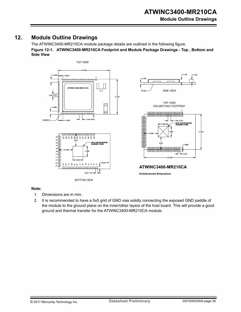