automatic extraction of behavioral models from simulations of
TRANSCRIPT
AUTOMATIC EXTRACTION OF BEHAVIORAL
MODELS FROM SIMULATIONS OF
ANALOG/MIXED-SIGNAL
(AMS) CIRCUITS
by
Satish Batchu
A thesis submitted to the faculty ofThe University of Utah
in partial fulfillment of the requirements for the degree of
Master of Science
Department of Electrical and Computer Engineering
The University of Utah
May 2011

Copyright c© Satish Batchu 2011
All Rights Reserved

The University of Utah Graduate School
STATEMENT OF THESIS APPROVAL
This thesis of Satish Batchu
has been approved by the following supervisory committee members:
Chris J. Myers , Chair 12/17/2010Date Approved
Kenneth S. Stevens , Member 12/17/2010Date Approved
Scott R. Little , Member 12/17/2010Date Approved
and by Gianluca Lazzi , Chair of
the Department of Electrical and Computer Engineering and by
Charles A. Wight, Dean of the Graduate School.

ABSTRACT
Verification of analog circuits is becoming a bottle-neck for the verification of com-
plex analog/mixed-signal (AMS) circuits. In order to assist functional verification of
complex AMS system-on-chips (SoCs), there is a need to represent the transistor-level
circuits in the form of abstract models. The ability to represent the analog circuits as
behavioral models is necessary, but not sufficient. Though there exist languages like
Verilog-AMS and VHDL-AMS for modeling AMS circuits, there is no easy method
for generating these models directly from the transistor-level descriptions. This thesis
presents an improved method for extracting behavioral models from the simulations
of AMS circuits. This method generates labeled Petri net (LPN) models that can be
used in the formal verification of circuits, and SystemVerilog models that can be used
in the system-level simulations.

To my advisor, Chris

CONTENTS
ABSTRACT . . . . . . . . . . . . . . . . . . . . . . . . . . . . . . . . . . . . . . . . . . . . . . . . . . iii
LIST OF FIGURES . . . . . . . . . . . . . . . . . . . . . . . . . . . . . . . . . . . . . . . . . . . . vii
LIST OF ALGORITHMS . . . . . . . . . . . . . . . . . . . . . . . . . . . . . . . . . . . . . . ix
ACKNOWLEDGEMENTS . . . . . . . . . . . . . . . . . . . . . . . . . . . . . . . . . . . . . x
CHAPTERS
1. INTRODUCTION . . . . . . . . . . . . . . . . . . . . . . . . . . . . . . . . . . . . . . . . . 1
1.1 Motivation . . . . . . . . . . . . . . . . . . . . . . . . . . . . . . . . . . . . . . . . . . . . . . 11.2 Related Work . . . . . . . . . . . . . . . . . . . . . . . . . . . . . . . . . . . . . . . . . . . . 31.3 Contributions . . . . . . . . . . . . . . . . . . . . . . . . . . . . . . . . . . . . . . . . . . . . 61.4 Thesis Overview . . . . . . . . . . . . . . . . . . . . . . . . . . . . . . . . . . . . . . . . . . 7
2. BACKGROUND . . . . . . . . . . . . . . . . . . . . . . . . . . . . . . . . . . . . . . . . . . . 9
2.1 Tool Flow . . . . . . . . . . . . . . . . . . . . . . . . . . . . . . . . . . . . . . . . . . . . . . . 92.2 Motivating Example . . . . . . . . . . . . . . . . . . . . . . . . . . . . . . . . . . . . . . 122.3 Simulation Data . . . . . . . . . . . . . . . . . . . . . . . . . . . . . . . . . . . . . . . . . . 142.4 Labeled Petri Net (LPN) . . . . . . . . . . . . . . . . . . . . . . . . . . . . . . . . . . . 14
2.4.1 LPN Syntax . . . . . . . . . . . . . . . . . . . . . . . . . . . . . . . . . . . . . . . . . 162.4.2 LPN Semantics . . . . . . . . . . . . . . . . . . . . . . . . . . . . . . . . . . . . . . 20
2.5 Verification Property . . . . . . . . . . . . . . . . . . . . . . . . . . . . . . . . . . . . . . 212.6 SystemVerilog . . . . . . . . . . . . . . . . . . . . . . . . . . . . . . . . . . . . . . . . . . . 23
3. MODEL GENERATION . . . . . . . . . . . . . . . . . . . . . . . . . . . . . . . . . . . . 26
3.1 Motivation . . . . . . . . . . . . . . . . . . . . . . . . . . . . . . . . . . . . . . . . . . . . . . 263.2 Overview . . . . . . . . . . . . . . . . . . . . . . . . . . . . . . . . . . . . . . . . . . . . . . . 293.3 Generation of an LPN Process . . . . . . . . . . . . . . . . . . . . . . . . . . . . . . . 323.4 Dealing with Transient Behavior . . . . . . . . . . . . . . . . . . . . . . . . . . . . . 39
3.4.1 Initial Transient . . . . . . . . . . . . . . . . . . . . . . . . . . . . . . . . . . . . . . 393.4.2 Intermediate Transient . . . . . . . . . . . . . . . . . . . . . . . . . . . . . . . . 43
3.5 Generalizing the Extracted LPN . . . . . . . . . . . . . . . . . . . . . . . . . . . . . 463.5.1 Functional Approach . . . . . . . . . . . . . . . . . . . . . . . . . . . . . . . . . . 483.5.2 Pseudo-Transitions . . . . . . . . . . . . . . . . . . . . . . . . . . . . . . . . . . . 553.5.3 Limitations . . . . . . . . . . . . . . . . . . . . . . . . . . . . . . . . . . . . . . . . . 58
3.6 Conversion to SystemVerilog . . . . . . . . . . . . . . . . . . . . . . . . . . . . . . . . 59

4. CASE STUDIES . . . . . . . . . . . . . . . . . . . . . . . . . . . . . . . . . . . . . . . . . . . 63
4.1 Phase Interpolator . . . . . . . . . . . . . . . . . . . . . . . . . . . . . . . . . . . . . . . . 634.2 Voltage Controlled Oscillator (VCO) . . . . . . . . . . . . . . . . . . . . . . . . . . 68
5. CONCLUSIONS . . . . . . . . . . . . . . . . . . . . . . . . . . . . . . . . . . . . . . . . . . . 79
5.1 Summary . . . . . . . . . . . . . . . . . . . . . . . . . . . . . . . . . . . . . . . . . . . . . . . 795.2 Future Work . . . . . . . . . . . . . . . . . . . . . . . . . . . . . . . . . . . . . . . . . . . . 80
5.2.1 Linear Interpolation of Assignments . . . . . . . . . . . . . . . . . . . . . . 805.2.2 Generation of stable Using a Functional Approach . . . . . . . . . . . 815.2.3 Embedding Limitations Within the Model . . . . . . . . . . . . . . . . . 815.2.4 Guidance for Additional Simulations . . . . . . . . . . . . . . . . . . . . . . 815.2.5 Equivalence Checking . . . . . . . . . . . . . . . . . . . . . . . . . . . . . . . . . 825.2.6 Extension of LPNs to Express Temporal Properties . . . . . . . . . . 825.2.7 Application to Other Hybrid System Models . . . . . . . . . . . . . . . . 83
REFERENCES . . . . . . . . . . . . . . . . . . . . . . . . . . . . . . . . . . . . . . . . . . . . . . . . 84
vi
LIST OF FIGURES
2.1 Tool flow. . . . . . . . . . . . . . . . . . . . . . . . . . . . . . . . . . . . . . . . . . . . . . . . . 11
2.2 Schematic of a phase interpolator. . . . . . . . . . . . . . . . . . . . . . . . . . . . . . 12
2.3 SPICE simulation showing phase interpolation. . . . . . . . . . . . . . . . . . . . 13
2.4 Example LPN. . . . . . . . . . . . . . . . . . . . . . . . . . . . . . . . . . . . . . . . . . . . . 18
2.5 Environment model. . . . . . . . . . . . . . . . . . . . . . . . . . . . . . . . . . . . . . . . . 19
2.6 Portion of the phase interpolator simulation and corresponding LPN. . . 22
2.7 An example property LPN . . . . . . . . . . . . . . . . . . . . . . . . . . . . . . . . . . . 23
2.8 An example SystemVerilog model. . . . . . . . . . . . . . . . . . . . . . . . . . . . . . 25
3.1 An LPN model for the phase interpolator. . . . . . . . . . . . . . . . . . . . . . . . 27
3.2 Phase interpolator LPN with initial transients. . . . . . . . . . . . . . . . . . . . 42
3.3 Phase interpolator LPN with intermediate transients. . . . . . . . . . . . . . . 47
3.4 Example illustrating the addition of a transition to an LPN. . . . . . . . . . 52
3.5 Example illustrating the mergeTransitions operation. . . . . . . . . . . . . . 54
3.6 Phase interpolator LPN generated using a functional approach. . . . . . . 55
3.7 Phase interpolator LPN with pseudo-transitions. . . . . . . . . . . . . . . . . . . 57
3.8 The delay function. . . . . . . . . . . . . . . . . . . . . . . . . . . . . . . . . . . . . . . . . 61
3.9 Part of the SystemVerilog model for the phase interpolator. . . . . . . . . . 62
4.1 An LPN model for the 16 division phase interpolator. . . . . . . . . . . . . . . 64
4.2 Property LPN for a phase interpolator. . . . . . . . . . . . . . . . . . . . . . . . . . 66
4.3 SystemVerilog model for a phase interpolator. . . . . . . . . . . . . . . . . . . . . 67
4.4 A part of the simulation of a SystemVerilog model for a phase interpolator. 69
4.5 SPICE simulation of a VCO. . . . . . . . . . . . . . . . . . . . . . . . . . . . . . . . . . . 70
4.6 The LPN model for a VCO without control inputs and don’t cares. . . . 72
4.7 The LPN process for a VCO with a control input. . . . . . . . . . . . . . . . . . 73
4.8 The LPN process for assigning the stable variable. . . . . . . . . . . . . . . . . 74
4.9 The LPN process for a VCO demonstrating the transients, functionalapproach, and pseudo-transitions. . . . . . . . . . . . . . . . . . . . . . . . . . . . . . 75
4.10 Other LPN processes for the VCO model. . . . . . . . . . . . . . . . . . . . . . . . 76

4.11 Part of the SystemVerilog model for a VCO. . . . . . . . . . . . . . . . . . . . . . 77
4.12 Simulation of the SystemVerilog model for a VCO. . . . . . . . . . . . . . . . . 78
viii

LIST OF ALGORITHMS
3.1 genModel(N, C, Σ, par) . . . . . . . . . . . . . . . . . . . . . . . . . . . . . . . . . . . . . . 30
3.2 genProcess(N, c, Σ, θ, par) . . . . . . . . . . . . . . . . . . . . . . . . . . . . . . . . . . . 33
3.3 addStableVariable(N, c, Σ, θ) . . . . . . . . . . . . . . . . . . . . . . . . . . . . . . . 34
3.4 calculateDurations(σ, In,Out, reg) . . . . . . . . . . . . . . . . . . . . . . . . . . . 36
3.5 addInitialTransient(N, p0, σ, reg , c, dur, rate, val , θ) . . . . . . . . . . . . . . 41
3.6 addStableToData(σ, c, reg , dur, pre, par) . . . . . . . . . . . . . . . . . . . . . . . . 45
3.7 updateLPN(N, σ, i, reg , c, dur, pre, rate, val , θ) . . . . . . . . . . . . . . . . . . . . . 50
3.8 mergeTransitions(N) . . . . . . . . . . . . . . . . . . . . . . . . . . . . . . . . . . . . . . 53
3.9 insertPseudoTransitions(N, c, region, θ) . . . . . . . . . . . . . . . . . . . . . . 56

ACKNOWLEDGEMENTS
The past two years at the University of Utah has been an exciting journey for
me. Apart from the technical knowledge gained through regular coursework, I got an
exposure to different aspects of research through this thesis. This page will not be
sufficient to express my gratitude to my advisor, Chris Myers. From my experience,
Chris is the ideal advisor one can expect to have. Apart from giving me proper
guidance and encouragement throughout this process, he was very helpful and patient
in improving my writing skills. The most important of all are his great personal
qualities that I picked up in this course of time.
I would like to thank Ken Stevens and Scott Little for serving as my committee
members, and for providing valuable comments and suggestions. Scott in particular
was very co-operative and helpful by giving his thoughtful feedback at various phases
of this research. My summer internship at Intel was very useful in shaping this
research work. Thanks to Chris for his frequent visits and meetings that were very
helpful. I am very thankful to Chandramouli Kashyap, Murali Talupur, Chirayu
Amin, John O’Leary, Carl Seger, and Noel Menezes of Intel Corporation for their
valuable comments and discussions.
Thanks to the Semiconductor Research Corporation (SRC) for having faith in
this research and supporting this research for several years. SRC is very helpful in
supporting its students and in opening a number of opportunities to its students. I
thank Chris for giving me an opportunity to be a student member of SRC.
I thank my parents for providing constant encouragement and motivation without
having any clue about what I was up to. I do not think that I would have completed
my graduate studies successfully without their blessings and support. Lastly, I would
like to thank my labmates Kevin Jones, Robert Thacker, Curtis Madsen, and Zhen
Zhang for making our lab a wonderful place to work. Special thanks to my friend
Santosh Varanasi for helping me take the right decisions with his valuable insights.

CHAPTER 1
INTRODUCTION
Given a choice between having a car whose operation is completely mechanical
and one that relies on today’s advanced electronic circuits, many of us would opt
for a mechanical car. This is because most of the integrated circuits (ICs) which
are present in the products today are not tested exhaustively. The primary reason
for this is that there is no answer to the question, “When can we say that a chip,
comprising millions of transistors, has been verified thoroughly?” The only thing
that can be done is to ensure that the chip has been verified for as many test-cases
as possible before it reaches the end-product. With the ever-increasing complexity of
system-on-chips (SoCs) and the rapidly decreasing time-to-market, many SoC designs
reach the market or at least end up as first silicon without being tested adequately.
Thus, verification plays a key role in today’s industrial design flow, be it analog or
digital. The cost of a bug in the design grows exponentially with the time for which
it stays in the design without being caught. If a bug is found during the postsilicon
validation or later stages, then the chip has to be re-spun and it incurs a huge cost in
terms of time and money. So, it is important that a chip is tested adequately before
it is taped-out.
1.1 Motivation
The last few years have witnessed an increasing interest in integrating analog/
mixed-signal (AMS) circuits with application specific integrated circuit (ASIC) de-
signs. This is evident from the wide adoption of serial-signalling interfaces like
Serial-ATA, PCI-ExpressTM, and Ethernet. The primary intention of this integration
is to improve the turn-around time of ASICs by adopting SoC design approaches
[1]. Verification of these ICs turned out to be a very challenging task due to this
2
integration. This challenge can be attributed to the disparity between the conven-
tional verification methods of digital circuits and analog circuits. The techniques
used for verifying digital circuits are quite advanced while those used for analog
circuits are ad-hoc. Formal methods like equivalence checking and model checking
are proving to be very successful for the validation of digital designs. Advanced tools
and languages, which support techniques like constrained random stimulus generation
and assertion-based functional coverage analysis, have enabled the verification of
extremely complex digital designs [2, 3]. On the contrary, analog validation still
relies heavily on transistor-level simulations done using accurate differential equation
models and SPICE simulators. AMS circuits have been evolving rapidly over the past
few years. As these circuits evolve and tend to grow into larger components within a
chip, verifying the system adequately using traditional techniques becomes tedious.
Improving the verification quality of these complex SoCs comprising both digital and
AMS circuits requires either an impractical increase in the number of resources or the
usage of advanced verification methodologies.
Functional verification ensures that a circuit performs its intended function cor-
rectly. Functional verification is meant for catching functional bugs at early stages of
the design. Functional bugs can occur due to simple mistakes like incorrect connection
of the wires of a bus and connecting active high signals to active low inputs at an
interface. While SPICE is an efficient tool for performance verification, it is not a very
effective tool for functional verification of complex mixed-signal SoCs because of its
poor performance owing to high accuracy. As the complexity or size of a circuit being
simulated increases, the time required for SPICE simulation becomes a showstopper
for verifying the circuit adequately. Compromising the accuracy of the simulations to
a certain extent is tolerable while performing functional verification. This has been
a tradition followed for digital circuits since the invention of hardware description
languages (HDLs) and it has proved to be very successful in catching functional bugs
in the initial stages of the design. To bridge the gap between design and verification,
analog designers have to adopt a consistent verification methodology. Verification of
analog designs is complicated not only because analog signals are continuous in time

3
and value, but also due to the increasing process variability, number of parameters,
and physical effects which have to be considered.
Analog circuits can be verified using either formal methods or simulation methods.
Formal methods verify a system under all possible combinations of input signals and
for all possible states. This process is accomplished by finding the state-space of the
mixed-signal system. Simulation methods aim at simulating the whole system, which
is possible only by modeling the system components at various levels of abstraction
[4]. High-level modeling languages like Verilog-AMS and SystemVerilog are gaining
importance as abstract models tend to be a lot faster than transistor-level schematics
for simulation purposes. Recently, researchers have begun exploring the application
of formal methods to these circuits [5]. Various tools which have been developed
to explore the continuous state-space of AMS systems have showed some promising
results [6, 7, 8]. But a major challenge being faced by these tools is that the designer
has to model every system being verified, at an appropriate level of abstraction [9].
Given the complexity of mixed-signal circuits and the analog designers’ addiction
to the high accuracy SPICE simulations, creating accurate models can take a lot of
designers’ time and effort.
While having abstract models that are as accurate as the device-level transistor
models is desirable for the block-level designers, such an accuracy slows down system-
level verification. It is difficult to use a single abstract model for both circuit analysis
purposes of the designer and system-level verification purposes. Thus, a verification
methodology has to be compatible with the circuit analysis methods that an AMS
designer uses and at the same time be very efficient for system-level verification if
it has to be adopted widely [1]. Hence, tools capable of automatically generating
models at the appropriate level of abstraction can prove to be very useful to the AMS
community.
1.2 Related Work
Functional verification of complex mixed-signal SoCs is complicated by the fact
that the performance of a circuit analysis engine degrades exponentially with the size
of the circuit being analyzed. Though the FastSpice solvers [10, 11] perform better

4
than traditional SPICE on large circuits, they do that at the cost of reduced accuracy
and a large dependence on the nature of the circuit [1]. Other disadvantages with
relying on FastSpice for functional verification are that it is utilized too late in the
design cycle when the complete transistor-level design of the system is available and it
is too slow for simulating the whole system in all the modes of operation. There exist
advanced simulation techniques for periodic steady state (PSS) analysis of analog
circuits [12], but they do not apply to large mixed-signal circuits, which generally
do not provide those basic periodic conditions. Transient simulation is an option
for verification of such circuits, especially radio-frequency (RF) front-ends with very
high carrier frequencies, but it requires a lot of simulation time and computational
power [13]. Methods for generating coverage-guided test cases and for generating
input stimuli which cover every possible state that a continuous system can adopt
have been discussed in [14, 15]. In [16], the authors describe a way of finding the
test cases that characterize an AMS circuit and its application for evaluating the
equivalence between a circuit and its behavioral model. However, simulating an SoC
such that all these stimuli are applied to the AMS circuit for every unique input to
the rest of the system takes a prohibitively large amount of time. Abstract modeling
of subsystems and circuits using HDLs can solve these problems because HDLs are
capable of modeling just the circuit behavior by ignoring the lower-level details. The
improvement in the simulation performance is a result of the loss in accuracy.
In [17], the authors develop behavioral models which specify custom memory
structures as interacting state machines. However, this method is applicable only to
memory designs with regular components. Various techniques for abstracting linear
systems have shown promising results [18, 19], but there are not many successful
methods for accurately modeling nonlinearities of AMS circuits. The approaches used
for modeling nonlinear systems rely on approximating them as either piecewise linear
or picewise polynomial and then applying the abstract modeling techniques of the
linear or weakly nonlinear systems [20, 21]. The piecewise linear approximation leads
to difficulties in modeling the higher order systems while the piecewise polynomial
approximation necessitates complex ways of selecting the inputs [22]. Since analog
designers simulate their circuits for a variety of inputs which when applied to the

5
circuit is expected to work properly, generating abstract models from simulation data
does not require significant additional work by the designer. This has created an
increasing interest in simulation-aided verification (SAV) techniques. One of the
approaches to verify AMS circuits proves the correctness of a circuit by finding a
finite number of simulation traces that are sufficient to represent all trajectories of the
system [23]. Other approaches include verification of formal properties on simulation
traces directly [24, 25], and generation of a formal model from simulation traces,
which can be analyzed using state space exploration techniques [26]. Dastidar et
al. generate a finite state machine (FSM) from a set of simulation traces [26]. An
acyclic FSM is generated using currents, voltages, and time as state variables. The
state space of the system is divided symmetrically into state divisions. The state of
the simulator is determined after every delta time step, and rounded to the center of
the appropriate state division. The simulator is then started from here and run for
the next delta time step. This process is done until the global time reaches a user
specified maximum.
LPN Embedded/Mixed-signal Analyser (LEMA) is a tool that takes simulation traces
of AMS circuits and generates formal models in the form of labeled petri nets (LPNs)
and AMS HDL models in the form of Verilog-AMS and VHDL-AMS [22]. The LPN
models are meant to be verified formally using various model checking techniques [27].
The AMS HDL models can be integrated with the behavioral models of the rest of the
ASIC for performing fast system-level simulations which verify the functionality of
the system as a whole. The approach used in LEMA is similar to that of Dastidar et al.
The state space is divided into regions based on thresholds on signal values, which can
either be provided by the user or generated automatically. The obtained graphs may
be cyclic because a global timer is not one of the state variables. Since the information
from simulation traces is captured from start to finish without stopping anywhere,
the models generated by LEMA preserve the original simulation traces. Using this
approach, the model allows for dynamic variation of parameters. Standard simulation-
based methods allow for changes in initial conditions and parameters, but these values
are then fixed for the duration of the simulation run. Simulation of an LPN model
allows the system to be explored under ranges of initial conditions as well as ranges of

6
dynamically changing parameter values. This additional behavior helps in discovering
errors caused by variations [9]. However, using this method, the number of simulations
required for generating a model that produces reasonably good results in all the test
conditions can be very high.
1.3 Contributions
This thesis presents an improved method for extracting behavioral models from
simulations of AMS circuits. This method allows the extracted behavioral models
to replace the original transistor-level circuits in the complex mixed-signal SoCs,
thus improving the performance of system-level simulations. The abstract models
generated by this method are LPNs which can be verified formally and HDL models
which can be simulated for correctness. The new method has been implemented in the
tool LEMA such that LPN and SystemVerilog models can be extracted automatically
from the simulation traces of AMS circuits. The method presented here enables the
extraction of models which have different levels of accuracy and generality based on
the algorithms used. The three major contributions of this research are :
• A method to represent transient behavior, present in simulation traces, in the
LPN models.
• Generalization while extracting the LPN models so that they can be subjected
to arbitrary stimuli for simulation purposes.
• A generic way of representing the extracted LPN models in HDLs like Sys-
temVerilog and automatic translation of LPNs to SystemVerilog accurately.
A real analog circuit always has a finite settling time before it attains a steady-state
frequency, voltage, etc. If this is not taken into consideration while extracting models
from the simulations, the generated models are not accurate representations of the
actual circuits. These transients can be present at the start of the simulation or
whenever there is a change in the mode of operation. The first contribution of this
research is a solution to the above problem in which a binary state variable is added
when a circuit has transient effects. The addition of binary variable isolates the
transient behavior from the steady-state behavior of the model.
7
An LPN model generated from a set of simulation traces is just as good as the
simulation traces from which it is generated. In other words, it produces correct
results only when it is subjected to sequences of stimuli which are exactly the same
as those used for generating it. For any other sequence of stimuli, the results are
unpredictable and there is a possibility of deadlock. The second contribution of this
thesis is the extension of the applicability of these models by generalizing them during
model generation. Two methods for doing this are discussed.
• Addition of pseudo-transitions.
• A functional approach.
The LPN models generated from simulations cannot be simulated with any of the
standard tools used in industry. Also, if they cannot be integrated with the HDL
models of other digital blocks in the system, then their practical use is very limited.
In order to apply this model generation approach to real world examples, the LPN
models have to be represented accurately in industry-standard HDLs. Though they
can be represented in Verilog-AMS, the simulation performance is limited by by the
continuous-time kernel of the mixed-signal simulator. For this reason, the LPN models
are being represented in SystemVerilog which runs on the discrete-event kernel. The
third contribution of this thesis is an approach for accurate translation of LPNs in
SystemVerilog while complying with the LPN semantics.
1.4 Thesis Overview
The rest of this thesis is organized as four chapters which give a detailed descrip-
tion of the contributions of this research. Chapter 2 gives an overview of the LEMA
tool’s model generator. It also provides the mathematical definition of an LPN along
with its graphical description, and shows how the LPNs are capable of modeling AMS
circuits. A brief introduction to SystemVerilog is given and the reason for choosing
SystemVerilog as the HDL is detailed.
Chapter 3 describes the model generation algorithm in detail. The approach
used to distinguish the steady-state behavior from the transient behavior present in
the simulation traces is discussed. It is also shown how the same method applies for
8
separating the initial portion of the simulations, which does not account for the actual
circuit’s functionality, from the relevant portion of the circuit’s simulation. Different
methods of generalizing the model such that it can be simulated with arbitrary stimuli
are discussed. The advantages and disadvantages of these approaches are mentioned
so that one knows when to choose a particular method. This chapter also describes
the method used to translate an LPN to SystemVerilog. A number of subtleties in the
LPN semantics are shown and the way in which this method allows correct translation
of the LPN semantics to SystemVerilog is demonstrated.
Chapter 4 presents industrial examples like a phase interpolator and a voltage
controlled oscillator (VCO). The LPN models generated using the improved model
generation approach are shown which demonstrate the importance of the methods
presented in Chapter 3. Property LPNs which are used to formally verify the func-
tionality of these models are also shown. The same property LPNs get translated
to assertions upon converting the LPN model to SystemVerilog. The SystemVerilog
models are simulated and the functionality is verified by means of assertions. These
examples also show how the methods presented here are directly applicable to the
accurate and generalized modeling of industrial circuits.
Chapter 5 summarizes the research work detailed in this thesis. The scope and
results of this research are also presented. This chapter also describes a number of
interesting areas where this research is applicable directly or indirectly. While this
work solves some of the problems related to model extraction, there are numerous
interesting problems that still need to be addressed. The future work section of this
chapter describes some such problems which need to be addressed.

CHAPTER 2
BACKGROUND
The first section of this chapter introduces a tool flow that is easy to integrate with
the current industrial design and verification flows of AMS circuits. Then, it is shown
how the method of model generation described in Chapter 3 fits into this tool flow
without any extra burden on the designers. The later sections provide the background
information that is useful in understanding the model generation method described
in the following chapters. A phase interpolator example circuit, which served as a
motivation for many improvements in the model generation method, is presented.
The LPNs are explained mathematically and their graphical representation is shown.
A brief introduction to SystemVerilog, which is the HDL into which the LPNs get
translated, is provided.
2.1 Tool Flow
The complexity of digital circuits that are being shipped as ASICs has increased
tremendously over the past two decades. This advancement has been possible primar-
ily due to the improvements in the design automation tools which deal with Boolean
logic. For instance, today’s design automation tools for digital circuits are capable of
synthesizing multimillion gate circuits from high-level HDL descriptions of the desired
functionality, checking the equivalence of the HDL model and synthesized circuit,
verifying the generated circuit for arbitrary test cases which a human brain may not
even think of, etc. Many of these tools are capable of dealing with different models
of the same circuit that differ just in the level of abstraction. Digital circuits are
typically represented at RTL, gate-level, transistor-level, and layout-level abstractions
only. On the contrary, analog circuits are generally represented at circuit-level and
layout-level abstractions. Though they can be represented in HDLs like Verilog-AMS

10
and VHDL-AMS, they can neither be synthesized to transistor-level designs nor be
verified as an equivalent description of an already designed transistor-level schematic.
State machines are the ubiquitous representation for digital circuits, and most
tools utilize them. It is important that AMS circuits have a similar formal model
that can be analyzed easily by design automation tools. It is not just sufficient to
have a model that is an accurate abstract representation of an AMS circuit. The
model should be easily obtainable by leveraging the existing design methodologies.
In other words, modeling the circuit should require minimal efforts of the designer
because the designers are not expected to model the circuits manually. If they have
to do that, then the same design exists at two places and every small change in the
design needs to be ported manually to the model and vice versa. This is not a good
practice because of the high probability for inconsistencies between the model and
the circuit. For simulation purposes, the model should also be representable in the
industry-standard HDLs.
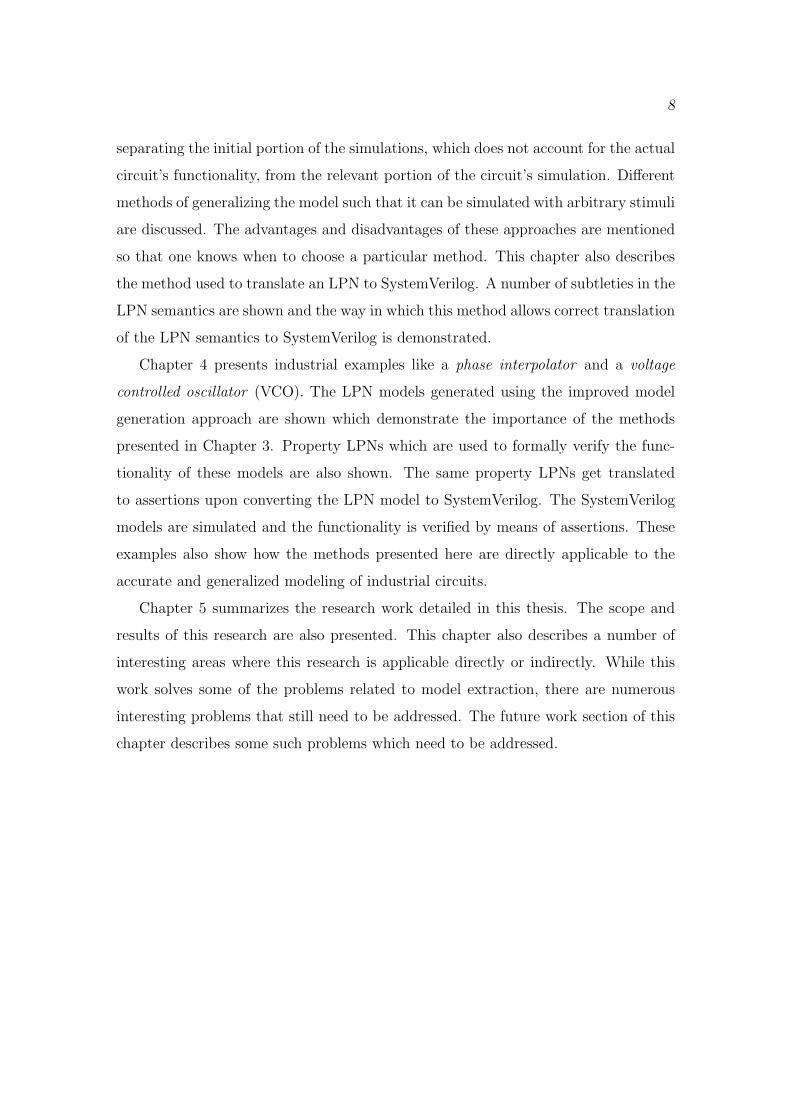
SAV [22] is a methodology developed with the above requirements in mind. Fig. 2.1
shows the verification flow using the SAV methodology that can be integrated with the
current industrial design and verification flows. The top portion of the figure shows
the traditional AMS verification process where the designer simulates the design for
a number of test configurations and ensures that the performance and functionality
requirements are met by observing the simulation traces. This is an iterative process.
The model generator shown in the figure takes the set of simulation data that the
designer used to verify the circuit and an optional verification property and generates
an LPN model and a SystemVerilog model. The LPN models can be verified using
model checking approaches. The SystemVerilog model generated for the AMS circuit
can be integrated with the RTL models of the digital logic and simulated using the
traditional techniques used for functional verification of digital logic. The model
generator also translates the verification properties to SystemVerilog assertions which
can be used to analyze the functional coverage of the test-bench. The remainder of
this chapter describes the inputs accepted and the outputs produced by LEMA which
is a tool that implements the verification flow mentioned above.
11
Analog Circuit
Petri Net (LPN)
Simulation
Engine
SimulationTraces
Model
Checker
Transistor Level Design
VerificationProperty
SystemVerilog
Model
Assertion
Pass/Fail
RTL for Digital
Components
Pass or Fail+
Error Trace
SPICE
Model
Generator
Verification
Traditional
Labeled
Figure 2.1: Tool flow.
12
2.2 Motivating Example
A phase interpolator example is used in Chapter 3 to illustrate the improved
method for generating models from simulation traces. Phase interpolating circuits
are commonly used in the receivers of serial communication links for adjusting the
phase of the sampling clocks in fine increments. Fig. 2.2 shows the transistor-level
schematic of one block of the phase interpolator with symmetric load [28]. This block
has two unit cells, each clocked by differential clocks phi and psi.
A typical phase interpolator has 16 such blocks connected to the differential
output, omega and omegab. Thermometer encoded control lines, ctl[15:0], are used
to control the phase of the output signal omega by mixing the phases of phi and
psi in an appropriate ratio. Fig. 2.3 shows 16 SPICE simulations of such a phase
interpolator, each for a different value of ctl. It can be observed that the phase of the
output is different in all the simulations, and hence is adjusted as the value of ctl is
changed.
Vbp
.
Vdd
16 similar blocks
for i = 0...15
Vbn
.. . .
Vdd
.
.. .
..
ctl [i]
omega
omegab
psibphib psiphi
ctlb[i]
Figure 2.2: Schematic of a phase interpolator.

13
Fig
ure
2.3:
SPICE
sim
ula
tion
show
ing
phas
ein
terp
olat
ion.

14
2.3 Simulation Data
Our SAV methodology generates abstract models using the data obtained by
simulating a circuit in a simulator like SPICE. Simulation data is a tuple of the form
〈S, Σ〉, where S is the set of all design variables in the circuit being modeled, and Σ is
the set of time series simulation traces. Each trace σ ∈ Σ is an n-tuple 〈τ, ν0, . . . , νn−1〉
where τ ∈ R is the timestamp for the data points (ν0, . . . , νn−1) ∈ Rn where n is |S|.
Table 2.1 is an example which shows the type of simulation data that can be
obtained by simulating circuits in SPICE. The data in this table correspond to a phase
interpolator simulation in which ctl is varied sequentially through the thermometer
code sequence 1 to 3, and is used to generate the LPN models described in Chapter 3.
For the sake of simplicity, the differential signals have been replaced by single-ended
signals. The two clock inputs, phi and psi, have equal frequencies and are separated
in phase by 90 degrees.
These data show the voltages of the signals, ctl, phi, and omega, which are recorded
at a timestep of 20 ps for a duration of 48 ns. To access the timestamp for data point
i, the notation σi(τ) is used. Similarly, to access the data value i for variable ν, the
notation σi(ν) is used. In Table 2.1, σ1(τ) is 20 ps and σ1(phi) is −2.5 V.
2.4 Labeled Petri Net (LPN)
LPNs are the formal models used to represent AMS circuits in LEMA. They are a
variant of Petri Nets which have extended semantics that allow modeling of hybrid
systems and embedded systems. Hybrid Petri nets (HPN) and hybrid automata were
developed to represent systems which have continuously varying signals [29, 30, 31,
32]. As these formalisms are not easily compiled from high-level languages, labeled
hybrid Petri nets (LHPNs) were developed [33, 34]. LHPNs have been generalized as
LPNs due to the recent extensions which enable them to model embedded systems
which typically contain software, digital systems, and analog circuitry [35].
The LPNs generated using the methods presented in Chapter 3 are the simplest
forms of LPNs because the individual processes of these LPNs do not have con-
currency. In other words, each process has exactly one token at any instant and
hence the generated LPNs are essentially extended state machines. LPNs differ

15
Table 2.1: Part of the simulation data of a phase interpolator.
Time phi ctl omega
(ps) (V) (V)0 -2.5 1 1.7738720 -2.5 1 1.77306...
......
...120 -2.5 1 1.77349140 2.5 1 1.77411160 2.5 1 1.77436...
......
...1500 2.5 1 1.995511520 2.5 1 1.02016
......
......
2120 2.5 1 2.499812140 -2.5 1 2.499792160 -2.5 1 2.49981
......
......
3880 -2.5 1 2.021903900 -2.5 1 2.00266
......
......
4120 -2.5 1 1.860984140 2.5 1 1.853664160 2.5 1 1.84671
......
......
15980 -2.5 1 1.9419416000 -2.5 2 1.9284516020 -2.5 2 1.91594
......
......
16120 -2.5 2 1.8673416140 2.5 2 1.8603016160 2.5 2 1.85361
......
......
31980 -2.5 2 1.9330132000 -2.5 3 1.92046
......
......
47980 -2.5 3 1.92376
16
from standard state machines in that they contain rates, real values, delays, etc.
which allow modeling of continuous and asynchronous signals. LPNs also allow for
nondeterminism in all the above parameters. The syntax of the LPNs that are
generated from simulation traces is described in Section 2.4.1. Section 2.4.2 gives
a brief explanation of LPN semantics which is essential to understand the model
generation procedure described in Chapter 3. A detailed description of the complete
syntax and semantics of general LPNs is given in [33, 34, 35].
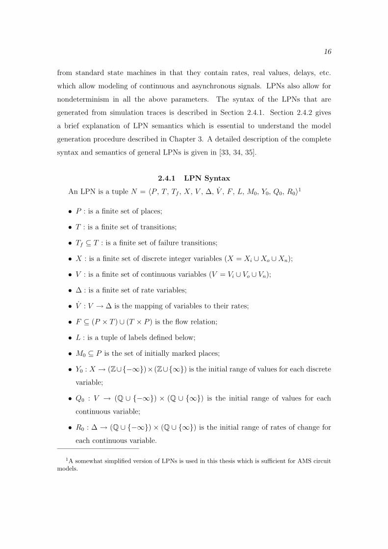
2.4.1 LPN Syntax
An LPN is a tuple N = 〈P , T , Tf , X, V , ∆, V , F , L, M0, Y0, Q0, R0〉1
• P : is a finite set of places;
• T : is a finite set of transitions;
• Tf ⊆ T : is a finite set of failure transitions;
• X : is a finite set of discrete integer variables (X = Xi ∪Xo ∪Xn);
• V : is a finite set of continuous variables (V = Vi ∪ Vo ∪ Vn);
• ∆ : is a finite set of rate variables;
• V : V → ∆ is the mapping of variables to their rates;
• F ⊆ (P × T ) ∪ (T × P ) is the flow relation;
• L : is a tuple of labels defined below;
• M0 ⊆ P is the set of initially marked places;
• Y0 : X → (Z∪{−∞})× (Z∪{∞}) is the initial range of values for each discrete
variable;
• Q0 : V → (Q ∪ {−∞}) × (Q ∪ {∞}) is the initial range of values for each
continuous variable;
• R0 : ∆ → (Q ∪ {−∞}) × (Q ∪ {∞}) is the initial range of rates of change for
each continuous variable.
1A somewhat simplified version of LPNs is used in this thesis which is sufficient for AMS circuitmodels.

17
where Xi, Xo, and Xn are the discrete integer input, output, and internal variables,
respectively, and Vi, Vo, and Vn are continuous input, output, and internal variables,
respectively.
Fig. 2.4 is a graphical representation of an example LPN that is generated from
simulation traces for the phase interpolator. Circles labeled p0 to p5 are places which
represent the states of the LPN (i.e., P = {p0, . . . , p5}). The tokens in the LPN
move between places by the firing of transitions, which are named t0 to t7 in the
figure (i.e., T = {t0, . . . , t7}). The figure shows that p0 has a token indicating that
this place is initially marked (i.e., M0 = {p0}). The arcs connecting the places and
the transitions represent the flow relation, F . This example LPN only has discrete
variables, ctl, phi, and omega (i.e., X = {ctl, phi, omega}). The variables ctl and
phi are input variables, and omega is an output variable for this LPN (i.e., Xi =
{ctl, phi}, Xo = {omega}, Xn = ∅). The general LPN would also have continuous
variables. The lack of continuous variables in this LPN implies that there are no rate
variables (i.e., V = ∆ = ∅). Though the simulation data in Table 2.1 show that phi
and omega are continuously varying signals, they have been abstracted by the SAV
method as discrete variables. The initial values of ctl, phi, and omega are 1, -2.5,
and 2, respectively. An LPN with continuously-varying variables would have initial
rates of change for the same.
A process is a connected set of places and transitions in an LPN. Every transition
t ∈ T has a preset denoted by •t = {p | (p, t) ∈ F} and a postset denoted by t• = {p |
(t, p) ∈ F}. Similarly, every place has a preset denoted by •p = {t | (t, p) ∈ F} and a
postset denoted by p• = {t | (p, t) ∈ F}. Fig. 2.5 shows the environment model that
is generated from simulation traces for the phase interpolator. It comprises of two
processes — the first comprising transitions t8 and t9 models a phase interpolation
selector, and the second process comprising transitions t10 and t11 models a clock
generator.
Each transition in an LPN may have one or more labels, each of which is either
an enabling condition or an assignment. The numerical portion of the grammar, χ,
used by these labels is described below:
χ ::= ci | ∞ | xi | vi | vi | (χ) | − χ | χ + χ | χ ∗ χ | INT(φ) | uniform(χ, χ)

18
p2
phi:=
-2.5
ctl:=
1
t3t4
{¬(p
hi≥
0)}
<om
ega:
=unifor
m(1
.9,2
)>
t6
<om
ega:
=unifor
m(1
.9,2
)>[u
nifor
m(1
720,
1730
)]
{¬(p
hi≥
0)}
<om
ega:
=unifor
m(2
.4,2
.5)>
[unifor
m(1
260,
1300
)]
{(ct
l≥
2.5)∧
(phi≥
0)}
t7
[unifor
m(1
740,
1750
)]
t0{¬
(ctl≥
1.5)∧
(phi≥
0)} <om
ega:
=unifor
m(1
.9,2
)><
omeg
a:=
unifor
m(2
.4,2
.5)>
t1{¬
(phi≥
0)}
[176
0][1
380]
[0]
[0]
{(ct
l≥
1.5)∧¬
(ctl≥
2.5)∧¬
(phi≥
0)}
t2t5
{(ct
l≥
2.5)∧¬
(phi≥
0)}
<om
ega:
=unifor
m(2
.4,2
.5)>
[unifor
m(1
320,
1360
)]
{(ct
l≥
1.5)∧¬
(ctl≥
2.5)∧
(phi≥
0)}
p3p
p4 p5p
p0 p1
p0
Init
ialva
lues
:
omeg
a:=
2
Fig
ure
2.4:
Exam
ple
LP
Nw
ith
six
pla
ces
and
eigh
ttr
ansi
tion
s.

19
p6
t10 t11
p7
t8[16000]
<ctl:=2>
<ctl:=3>
t9[16000]
<phi:=2.5> <phi:=-2.5>[uniform(140,2000)] [2000]
p8
p9p8
Figure 2.5: Environment model.
where ci is a rational constant from Q, xi is a discrete variable, vi is a continuous
variable, and vi the rate of change of a continuous variable vi. The function INT
converts the Boolean true or false value to an integer 1 or 0, respectively. The
function uniform(l, u) returns a uniform random value between the lower and upper
bounds obtained by evaluating the expressions l and u. The set Pχ is defined as the
set of all formulae that can be constructed using the grammar χ. The Boolean part
of the grammar, φ, that the labels are allowed to use is as follows:
φ ::= true | false | ¬φ | φ ∧ φ | φ ∨ φ | χ ≥ χ
where ¬, ∧, and ∨ are Boolean negation, conjunction, and disjunction operators,
respectively. The set Pφ is defined as the set of all formulae that can be constructed
using the grammar φ.
The labels used as enabling conditions can only use a restricted subset of the χ and
φ grammars which are χe and φe, respectively. The numerical part χe does not allow
the usage of continuous variables. In other words, enabling conditions are allowed to
have continuous variables only on the left side of the inequalities to ensure that the
right side of these relations is constant when time advances between transition firings.
The sets Pχeand Pφe
are defined as the set of all formulae that can be constructed
from the χe grammar and φe grammar, respectively.
20
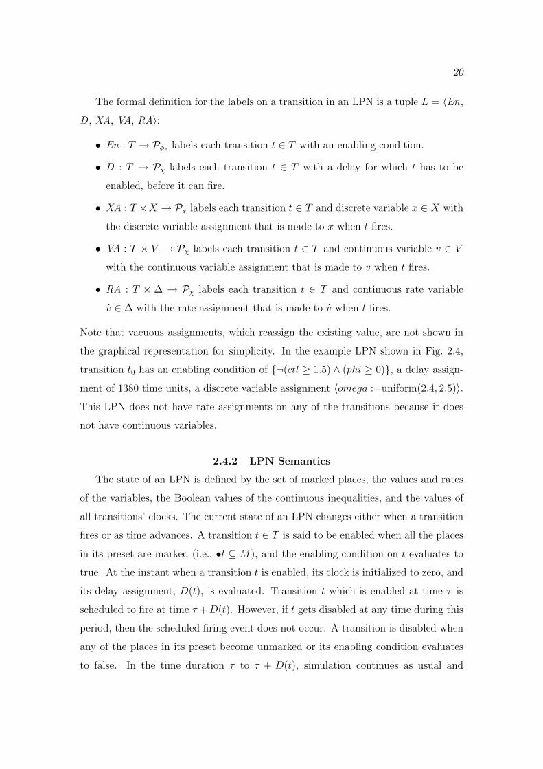
The formal definition for the labels on a transition in an LPN is a tuple L = 〈En,
D , XA, VA, RA〉:
• En : T → Pφelabels each transition t ∈ T with an enabling condition.
• D : T → Pχ labels each transition t ∈ T with a delay for which t has to be
enabled, before it can fire.
• XA : T ×X → Pχ labels each transition t ∈ T and discrete variable x ∈ X with
the discrete variable assignment that is made to x when t fires.
• VA : T × V → Pχ labels each transition t ∈ T and continuous variable v ∈ V
with the continuous variable assignment that is made to v when t fires.
• RA : T × ∆ → Pχ labels each transition t ∈ T and continuous rate variable
v ∈ ∆ with the rate assignment that is made to v when t fires.
Note that vacuous assignments, which reassign the existing value, are not shown in
the graphical representation for simplicity. In the example LPN shown in Fig. 2.4,
transition t0 has an enabling condition of {¬(ctl ≥ 1.5) ∧ (phi ≥ 0)}, a delay assign-
ment of 1380 time units, a discrete variable assignment 〈omega :=uniform(2.4, 2.5)〉.
This LPN does not have rate assignments on any of the transitions because it does
not have continuous variables.
2.4.2 LPN Semantics
The state of an LPN is defined by the set of marked places, the values and rates
of the variables, the Boolean values of the continuous inequalities, and the values of
all transitions’ clocks. The current state of an LPN changes either when a transition
fires or as time advances. A transition t ∈ T is said to be enabled when all the places
in its preset are marked (i.e., •t ⊆ M), and the enabling condition on t evaluates to
true. At the instant when a transition t is enabled, its clock is initialized to zero, and
its delay assignment, D(t), is evaluated. Transition t which is enabled at time τ is
scheduled to fire at time τ +D(t). However, if t gets disabled at any time during this
period, then the scheduled firing event does not occur. A transition is disabled when
any of the places in its preset become unmarked or its enabling condition evaluates
to false. In the time duration τ to τ + D(t), simulation continues as usual and
21
other transitions can be enabled or disabled due to the fact that the inequalities can
change at any instant. When a transition fires, the marking is updated by deleting
the tokens from the places in its preset and adding tokens to the places in its postset.
Also, the discrete, continuous value, and continuous rate assignments associated with
the transition are performed, the state of the continuous inequalities are updated,
and the clocks associated with newly enabled transitions are initialized to zero.
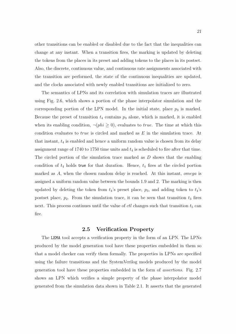
The semantics of LPNs and its correlation with simulation traces are illustrated
using Fig. 2.6, which shows a portion of the phase interpolator simulation and the
corresponding portion of the LPN model. In the initial state, place p3 is marked.
Because the preset of transition t4 contains p3 alone, which is marked, it is enabled
when its enabling condition, ¬(phi ≥ 0), evaluates to true. The time at which this
condition evaluates to true is circled and marked as E in the simulation trace. At
that instant, t4 is enabled and hence a uniform random value is chosen from its delay
assignment range of 1740 to 1750 time units and t4 is scheduled to fire after that time.
The circled portion of the simulation trace marked as D shows that the enabling
condition of t4 holds true for that duration. Hence, t4 fires at the circled portion
marked as A, when the chosen random delay is reached. At this instant, omega is
assigned a uniform random value between the bounds 1.9 and 2. The marking is then
updated by deleting the token from t4’s preset place, p3, and adding token to t4’s
postset place, p2. From the simulation trace, it can be seen that transition t3 fires
next. This process continues until the value of ctl changes such that transition t5 can
fire.
2.5 Verification Property
The LEMA tool accepts a verification property in the form of an LPN. The LPNs
produced by the model generation tool have these properties embedded in them so
that a model checker can verify them formally. The properties in LPNs are specified
using the failure transitions and the SystemVerilog models produced by the model
generation tool have these properties embedded in the form of assertions. Fig. 2.7
shows an LPN which verifies a simple property of the phase interpolator model
generated from the simulation data shown in Table 2.1. It asserts that the generated

22
p2
DA
Tim
e
p3
20,0
0021
,000
2.75
2.50
2.25
2.00
1.75
1.50
-2.7
5-2
.50
-2.2
5
omeg
a(X
)phi(X
)ct
l(X
)
t4
{(ct
l≥
1.5)∧¬
(ctl≥
2.5)∧
(phi≥
0)}
t5{(
ctl≥
2.5)∧¬
(ctl≥
3.5)∧¬
(phi≥
0)}
[0]
<om
ega:
=unifor
m(2
.4,2
.5)>
[unifor
m(1
320,
1360
)]
t3
<om
ega:
=unifor
m(1
.9,2
)>[u
nifor
m(1
740,
1750
)]{¬
(phi≥
0)}
{(ct
l≥
1.5)∧¬
(ctl≥
2.5)∧¬
(phi≥
0)}
[0]
t2
E
1.25
1.00
0.75
0.50
0.25
0.00
-0.2
5-0
.50
-0.7
5-1
.00
-1.2
5-1
.50
-1.7
5-2
.00
16,0
0017
,000
18,0
0019
,000
Fig
ure
2.6:
Por
tion
ofth
ephas
ein
terp
olat
orsi
mula
tion
and
corr
espon
din
gLP
N.

23
Tf = {t12}
[0]
t12
p10
{¬(ctl ≥ 0.5) ∨ (ctl ≥ 3.5)}
Figure 2.7: An example property LPN.
model is functional only when the value of ctl is within the range [0.5,3.5). In this
LPN, the set of failure transitions, Tf , includes the single transition t12.
2.6 SystemVerilog
SystemVerilog is a language developed with the intent of being useful both as an
HDL and as a hardware verification language (HVL). It is based on IEEE 1364TM
Verilog language and has extensions which make it easy to write test-benches and
allow for reuse of verification intellectual property (IP) [2]. While there are dedi-
cated languages like Verilog-AMS and VHDL-AMS which are capable of modeling
AMS circuits, SystemVerilog is chosen for several reasons the primary reason being
SystemVerilog models simulate only on a discrete-event kernel whereas the models
described in the AMS HDLs mentioned above need a mixed-signal simulator which has
a continuous-time kernel and a discrete-event kernel. Though simulation of models
written in HDLs like Verilog-AMS is faster when compared to SPICE simulation, the
improvement in performance degrades as the amount of code in the analog block,
which uses the continuous-time kernel, of the Verilog-AMS model increases [36]. For
system-level verification where performance of the simulations is critical, it is better
to have models which are very efficient if they have sufficient accuracy. The LPN
models extracted from the simulation traces can be described in SystemVerilog with
a slight compromise in accuracy. Instead of Verilog, SystemVerilog is chosen because

24
SystemVerilog allows real-valued ports for its modules which can be used to model
continuously varying signals of analog circuits.
Fig. 2.8 shows an example SystemVerilog model that is equivalent to the LPN
shown in Fig. 2.4. The code within the module and endmodule statements describes
a hierarchical block in a design. Modules enforce hierarchy by communicating through
a set of input, output, and bidirectional ports. The block of code within the begin
and end statements that follow an initial statement is called an initial block and is
used to set the initial state of the internal and output signals in the block. The assign
statement in SystemVerilog is a continuous assignment statement which evaluates the
expression on the right hand side whenever there is a change on any of the variables
of the expression. The result of the evaluation is assigned to the variable on the left
hand side after waiting for an inertial delay which follows the # symbol. The block of
code within the begin and end statements that follow an always statement is called an
always block. The list of signals or events that follow the always @ statement is called
a sensitivity list. The assignments inside the always block are procedural assignments
and are executed whenever an event is triggered by a change in any of the signals of
the sensitivity list. assert statements are generally used to describe properties of the
design that are meant to be satisfied always. In other words, assertions can be used
to verify properties on the design for a given set of simulations.

25
‘timescale 1ps/1fs
module phaseint(omega, phi, ctl);
input real phi, ctl;
output real omega;
logic p0, p1, p2, p3, p4, p5, p6, p7, p8, p9, p10;
wire t0, t1, t2, t3, t4, t5, t6, t7, t8, t9, t10, t11, t12;
initial beginomega = 2.0;
p0 = 1’b0;p1 = 1’b0;. . . ; p10 = 1’b0;
#1 p0 = 1’b1;p10 = 1’b1;
endassign #delay(∼ t0,1380) t0 = ∼(ctl≥1.5)&(phi≥0)&p0;
assign #delay(∼ t1,1760) t1 = ∼(phi≥0)&p1;
assign #delay(∼ t2,0) t2 = ∼(ctl≥2.5)&(ctl≥1.5)&∼(phi≥0)&p0;
• • •assign #delay(∼ t12,0) t12 = (∼(ctl≥0.5)‖(ctl≥3.5))&p10;
always @(posedge t0) beginp0 = 1’b0;
p1 = 1’b1;
omega = 2.5;
endalways @(posedge t1) begin
p1 = 1’b0;
p0 = 1’b1;
omega = 2.0;
endalways @(posedge t2) begin
p0 = 1’b0;
p2 = 1’b1;
end• • •
always @(t12)
assert(!t12)
else $error("Error! Assertion failure");
endmodule
Figure 2.8: An example SystemVerilog model.
CHAPTER 3
MODEL GENERATION
This chapter describes an improved method for generating LPN and SystemVerilog
models from simulations of analog circuits. Section 3.1 shows an LPN model that
is generated for a phase interpolator using the model generation method described
in [22]. This example is used to illustrate some of the problems that exist in this
approach. Sections 3.2 and 3.3 present an improved algorithm for generating models
from circuit simulations. In Section 3.4, the techniques used for solving problems faced
by the model generator when circuits have transient behavior are presented. Another
problem that is addressed is the limited applicability of the generated models. Sec-
tion 3.5 describes two techniques — insertion of pseudo-transitions and a functional
approach — to solve this problem and discusses their limitations. Section 3.6 describes
a new method for translating a general LPN to SystemVerilog while retaining the
original semantics of the LPN.
3.1 Motivation
It is customary for analog designers to simulate their circuits using a variety of
test-cases during the process of their design and verification. Little et al. developed the
tool LEMA which leverages the designer’s simulations to extract the circuit’s behavior
and represent it in the form of an abstract model [22]. Thus, this tool does not require
any additional work from the designer for getting behavioral models required for
system-level verification. At the same time, the designers are not required to change
their existing block-level verification methodologies for using this method. Fig. 3.1
shows an LPN model generated from the simulation data of a phase interpolator using
the method described in [22]. This model is supposed to describe the behavior of the
phase interpolator for three different values of ctl as observed in the given simulation

27
t4{¬
(phi≥
0)}
<om
ega:
=unifor
m(1
.9,2
)>
t6
[unifor
m(1
720,
1730
)]
{¬(p
hi≥
0)}
<om
ega:
=unifor
m(2
.4,2
.5)>
[unifor
m(1
260,
1300
)]
{(ct
l≥
2.5)∧
(phi≥
0)}
t7
[unifor
m(1
740,
1750
)]
t0{¬
(ctl≥
1.5)∧
(phi≥
0)} <om
ega:
=unifor
m(1
.9,2
)><
omeg
a:=
unifor
m(2
.4,2
.5)>
t1{¬
(phi≥
0)}
[176
0][1
380]
[0]
[0]
{(ct
l≥
1.5)∧¬
(ctl≥
2.5)∧¬
(phi≥
0)}
t2t5
{(ct
l≥
2.5)∧¬
(phi≥
0)}
<om
ega:
=unifor
m(2
.4,2
.5)>
[unifor
m(1
320,
1360
)]
{(ct
l≥
1.5)∧¬
(ctl≥
2.5)∧
(phi≥
0)}
<om
ega:
=unifor
m(1
.9,2
)>
p10
p6
p7 t9
<ct
l:=2>
[160
00]
t8
<ct
l:=3>
[160
00]
<phi:=
2.5>
[unifor
m(1
40,2
000)
]t1
0
<phi:=
-2.5
>
[200
0]t1
1[0
]
t12
{¬(c
tl≥
0.5)∨
(ctl≥
3.5)}
p2
p4
p3p
p5p
p1
p9
p8
p8
p0
Init
ialva
lues
:
omeg
a:=
2phi:=
-2.5
ctl:=
1
p0
t3
Fig
ure
3.1:
An
LP
Nm
odel
for
the
phas
ein
terp
olat
or.

28
trace. Though the abstract model need not be as accurate as a SPICE model, it still
has to represent the circuit’s behavior correctly.
Analog circuits typically need a finite response time before attaining a steady-
state. Generally, it is the steady state behavior which is of primary interest for func-
tional validation. The method described by Little et al. in [9] does not distinguish the
transient behavior from the steady-state behavior, and as a result of the conservative
approximations, the steady-state behavior includes the transient behavior as well.
This approach can potentially produce uninteresting models which show a combined
behavior from the circuit’s different operating modes when its operation is expected
to be distinct. For instance, transition t3 in the LPN shown in Fig. 3.1 has a delay
ranging from 1320 to 1360 ps. In reality, the circuit’s phase delay is changing from
1360 to 1320 ps for a short duration and after that, the delay is precisely 1320 ps.
In other words, though the circuit exhibits the properties of two different modes
only for a short duration when it switches from one mode to another, the generated
model includes the behavior of both the modes of operation for the complete duration
because the steady-state behavior is not distinguished from the transient behavior.
The models generated using Little’s method describe just the simulation traces
from which they are generated. Thus, these models are functional only when the in-
puts change in the sequence that occurred in the given simulation traces. The model’s
behavior is not correct for any other input combination. In a phase interpolator, the
value of ctl decides the phase offset of the output omega with respect to the input
phi, thus defining the mode of operation. The simulation trace used for generating
the model shown in Fig. 3.1 had ctl switching monotonically from 1 to 3 in steps of
1 and hence transitions t2 and t5 are the only transitions that can change the mode
of operation for this model. Consequently, this model deadlocks when the value of
ctl is changed from 2 to 1. This deadlock does not occur if the circuit’s simulation
trace has a situation where the value of ctl changes from 2 to 1. Simulating an analog
circuit for different modes of operation is possible, but it is not feasible to exercise all
possible permutations of the modes of operation. So, the models generated using this
method show a potential incorrect behavior even for the input combinations that are
29
present in the given simulations depending on the sequence of the input changes in
the simulation traces.
3.2 Overview
This chapter describes the function genModel which takes an initial LPN, N , a set
of components, C, a set of simulation traces, Σ, and a set of user-specified parameters,
par , and generates an LPN and a SystemVerilog model for the system. The given
initial LPN model, N , must contain all the design variables at a minimum, and is
included as part of the final LPN. Additionally, the initial LPN may also contain a
verification property. This feature is particularly useful for embedding verification
properties into the models of the circuit, much like the assertions embedded in
today’s register transfer level (RTL) designs. An application of property LPNs is
demonstrated in Chapter 4.
A component c = 〈In, Out, Care, Ctl〉 is a tuple comprising various subsets of the
system variables, S. Each component defines the interface of an LPN process that is
being constructed. In component c, In and Out are the inputs and the outputs of
an LPN process that is being constructed; Care and Ctl are the set of care variables
and control inputs for the process, respectively. For simplicity, it is assumed that
the outputs are a subset of care variables (i.e., Out ⊆ Care). The user-specified
parameters, par , that are used in generating the models include τmin, ǫ, ratio, ws , tol,
sig, and sep. The parameters, τmin, ǫ, and ratio, are used in the detection of DMV
variables. Calculation of rates for continuous variables is done using the window size
parameter, ws . Isolation of transient portions from the steady-state portions of the
simulations is done using the tolerance parameter, tol. The parameters, sig and sep,
are used in the normalization of the LPN model.
Algorithm 3.1 presents the genModel function which is an improved method for
extracting behavioral models from simulation traces. This function creates an LPN
process for each component c ∈ C, and then converts the generated LPN model to
SystemVerilog. A component is primarily used to describe the interface of a process
in the LPN that is being generated. Each process in the LPN is constructed based
on the interface described by its corresponding component. The user can specify the

30
Algorithm 3.1: genModel(N, C, Σ, par)
(X,V ) := detectDMV(V , Σ, par)1
θ := genThresholds(X,V , Σ, par)2
forall c = 〈In, Out, Care, Ctl〉 ∈ C do3
N := genProcess(N, c, Σ, θ, par)4
SV := convertToSystemVerilog(N)5
N := normalizeLPN(N , par)6
return (SV,N)7
circuit’s input/output interface or a system’s block-level connections in the form of a
set of components, C. Intuitively, each component, c = 〈In, Out, Care, Ctl〉, can be
thought of as a block in a system where In and Out are the inputs and the outputs
of the specific block that the component is representing; Care and Ctl are the set
of care variables and control inputs of the block, respectively. A variable is said to
be a care variable if the sequence in which it changes its region with respect to the
changes of other variables is an important aspect that needs to be encapsulated in
the generated model. The Care is the subset of continuous and DMV variables that
includes all the care variables in the circuit being modeled (i.e., Care ⊆ V ∪X). This
classification of variables is used in the functional approach described in Section 3.5.1.
The inputs of a circuit which when triggered cause the circuit to show a transient
behavior that is different from the steady-state behavior for a finite time duration are
called control inputs. The notion of control inputs is used to encapsulate the transient
and the steady-state behaviors separately in the generated models as described in
Section 3.4.2. As the name implies, control inputs, Ctl, are a subset of the input
variables, In.
In this method, all the signals in a circuit are classified as either continuous
or discrete multi-valued (DMV) variables. DMV variables are the variables which
are stable most of the time. They are useful in abstracting the continuous-time
continuous-valued signals that are stable most of the time as continuous-time discrete-
valued signals. DMV variables are also useful in modeling buses comprised of multiple
data lines as a single variable. Combining the individual lines of a bus in this way
reduces the number of state-variables and hence the complexity of the model. Fig. 3.1
shows that ctl[2:0], which are 3 individual thermometer-encoded inputs to the circuit,

31
are being combined and treated as a single DMV variable, ctl, in the generated model.
The improved method presented here is illustrated using example circuits which only
have DMV variables though the new techniques are directly applicable to circuits
with both types of signals.
The first step is to find the subset of the design variables, V , which are DMV. The
function detectDMV detects the DMV variables from the set of all variables, V , using
the given simulation traces, Σ, and the configurable parameters, τmin, ǫ, and ratio
(line 1). The τmin parameter specifies the minimum time duration for which a variable
has to be stable if this time has to count towards the total ratio of the waveform
duration for which it is stable. The ǫ parameter specifies the amount of tolerance
allowed for a variable to be treated as having a stable value. The ratio parameter
determines the minimum ratio of the waveform duration for which a DMV variable
has to be stable. A detailed description of the DMV variable detection method is
given in [22]. The above parameters can be configured such that continuous-valued
signals like clocks, which are stable most of the time, are abstracted as DMV variables.
At the end of this step, the disjoint sets X and V are updated such that the detected
DMV variables are moved from V to X.
To generate models, waveforms are split into regions which in turn are depicted
as places in the generated LPN. Splitting the waveform into regions is done using
the threshold values, θ, of the design variables. The ith region for variable ν is
defined as ξi(ν) = [θi(ν), θi+1(ν)) and the thresholds, θ, for each variable ν are
〈θ0(ν), . . . , θm(ν)〉 where θ1(ν) and θm−1(ν) are the lowest and highest real-valued
thresholds, respectively. θ0(ν) and θm(ν) are virtual and are set to −∞ and ∞,
respectively. Thus, the lowest region for variable ν is ξ0(ν) and the highest region
is ξm−1(ν). The function genThresholds generates the threshold values for all the
variables from the given set of simulation traces (line 2). Greedy algorithms are
used to auto-generate thresholds for continuous variables [22]. To generate the
thresholds for the DMV variables, the stable values that each DMV variable has
in all the simulation traces are extracted. Thresholds for each DMV variable are
then determined as the medians of every two adjacent values from the detected set
of values of each variable.
32
The genProcess method generates an LPN process for every component using
its interface, simulation data, threshold values, and the user-specified parameters
(lines 3-4). The LPN model, N , is updated by integrating the LPN process generated
for each component. When a component with exactly the same input/output interface
as the actual circuit’s is used, it generates an LPN process that represents the circuit’s
behavior. A user can optionally provide other components that represent the blocks
that drive the circuit’s inputs. The resultant LPN model can be simulated as a
stand-alone system. The convertToSystemVerilog function converts the generated
LPN model to a SystemVerilog model that can be integrated with the HDL models
of the other digital blocks of the system for system-level simulations. A detailed
description of this function is given in Section 3.6. Finally, the normalizeLPN function
scales the values, delays, and rates on the transitions in the generated LPN using the
parameters, sig and sep, as described in [22]. The normalization step is intended
to add precision which aids the formal verification tool described in [22]. Thus,
the generated SystemVerilog model can be used with the simulation tools and the
normalized LPN model can be used with formal verification tools.
3.3 Generation of an LPN Process
Algorithm 3.2 presents the genProcess method which generates an LPN process
that it adds to N for a component c, from a set of simulation traces, Σ, using the
thresholds, θ, and user-specified parameters, par .The generation of every LPN process
begins by the addition of an initial place, whose postset transitions set the initial
states corresponding to each simulation trace. These transitions allow the model to
choose an initial state from any of the given simulation traces dynamically based
on the applied inputs. The addInitialPlace function adds this initial place to the
LPN (line 2). Control inputs are those inputs which can cause the circuit to display
a transient behavior that is different from its steady-state behavior for considerable
amount of time. To isolate such transient behavior from the steady-state behavior of
the model, the addStableVariable function adds a Boolean state variable, stable,
to the LPN and the simulation data if the circuit has any control inputs (lines 3-4).

33
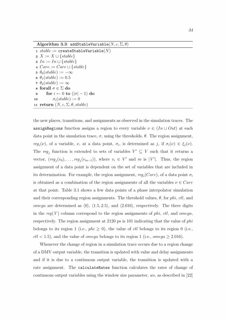
Algorithm 3.2: genProcess(N, c, Σ, θ, par)
let c = 〈In, Out, Care, Ctl〉1
(N, p0) := addInitialPlace(N)2
if Ctl 6= ∅ then3
(N, c, Σ, θ, stable) := addStableVariable(N, c, Σ, θ)4
forall σ ∈ Σ do5
reg := assignRegions(σ, In,Out, θ)6
rate := calculateRates(σ, Out, Care, reg , par)7
val := calculateValues(σ, Out, Care, reg , par)8
(dur, pre) := calculateDurations(σ, In,Out, reg)9
(N, i) := addInitialTransient(N, p0, σ, reg , c, dur, rate, val , θ)10
if Ctl 6= ∅ then11
(σ, reg) := addStableToData(σ, c, reg , dur, pre, par)12
rate := calculateRates(σ, Out, Care, reg , par)13
val := calculateValues(σ, Out, Care, reg , par)14
(dur, pre) := calculateDurations(σ, In,Out, reg)15
(N, region) := updateLPN(N, σ, i, reg , c, dur, pre, rate, val , θ)16
if Ctl 6= ∅ then17
cstable := 〈Ctl, {stable}, Ctl, ∅〉18
N := genProcess(N, cstable, Σ, θ, par)19
N := insertPseudoTransitions(N, c, region, θ)20
return N21
Algorithm 3.3 describes the steps involved in the addition of the stable variable
and initialization of the data values for stable. The createStableVariable function
creates a unique variable, stable, for each process having a nonempty set of control
inputs. Since this variable is Boolean, it is included in the set of DMV variables,
X, of the LPN. As the stable variable affects the behavior of the LPN process, it is
added to its input set, In, and the set of care variables, Care. The stable variable
being a Boolean has a single real threshold of 0.5. The variable stable is inserted in
the given set of simulation data and its value is initialized as 0 at all the data points.
Its actual value at each data point is determined as 0 or 1 depending on whether the
circuit is displaying transient behavior or steady-state behavior, respectively at that
point. A detailed description of this step is given in the addStableToData function
described in Section 3.4.2.
After the initialization of the stable variable, the genProcess function traverses
each of the given simulation traces and updates the LPN process incrementally with
34
Algorithm 3.3: addStableVariable(N, c, Σ, θ)
stable := createStableVariable(N)1
X := X ∪ {stable}2
In := In ∪ {stable}3
Care := Care ∪ {stable}4
θ0(stable) := −∞5
θ1(stable) := 0.56
θ2(stable) :=∞7
forall σ ∈ Σ do8
for i← 0 to (|σ| − 1) do9
σi(stable) := 010
return (N, c, Σ, θ, stable)11
the new places, transitions, and assignments as observed in the simulation traces. The
assignRegions function assigns a region to every variable ν ∈ (In ∪ Out) at each
data point in the simulation trace, σ, using the thresholds, θ. The region assignment,
reg i(ν), of a variable, ν, at a data point, σi, is determined as j, if σi(ν) ∈ ξj(ν).
The reg j function is extended to sets of variables V ′ ⊆ V such that it returns a
vector, (reg j(v0), . . . , reg j(vm−1)), where vi ∈ V ′ and m is |V ′|. Thus, the region
assignment of a data point is dependent on the set of variables that are included in
its determination. For example, the region assignment, reg i(Care), of a data point σi
is obtained as a combination of the region assignments of all the variables ν ∈ Care
at that point. Table 3.1 shows a few data points of a phase interpolator simulation
and their corresponding region assignments. The threshold values, θ, for phi, ctl, and
omega are determined as 〈0〉, 〈1.5, 2.5〉, and 〈2.016〉, respectively. The three digits
in the reg(V ) column correspond to the region assignments of phi, ctl, and omega,
respectively. The region assignment at 2120 ps is 101 indicating that the value of phi
belongs to its region 1 (i.e., phi ≥ 0), the value of ctl belongs to its region 0 (i.e.,
ctl < 1.5), and the value of omega belongs to its region 1 (i.e., omega ≥ 2.016).
Whenever the change of region in a simulation trace occurs due to a region change
of a DMV output variable, the transition is updated with value and delay assignments
and if it is due to a continuous output variable, the transition is updated with a
rate assignment. The calculateRates function calculates the rates of change of
continuous output variables using the window size parameter, ws , as described in [22]
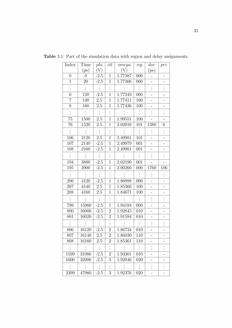
35
Table 3.1: Part of the simulation data with region and delay assignments.
Index Time phi ctl omega reg dur pre
(ps) (V) (V) (ps)0 0 -2.5 1 1.77387 000 - -1 20 -2.5 1 1.77306 000 - -...
......
......
......
...6 120 -2.5 1 1.77349 000 - -7 140 2.5 1 1.77411 100 - -8 160 2.5 1 1.77436 100 - -...
......
......
......
...75 1500 2.5 1 1.99551 100 - -76 1520 2.5 1 2.02016 101 1380 6...
......
......
......
...106 2120 2.5 1 2.49981 101 - -107 2140 -2.5 1 2.49979 001 - -108 2160 -2.5 1 2.49981 001 - -...
......
......
......
...194 3880 -2.5 1 2.02190 001 - -195 3900 -2.5 1 2.00266 000 1760 106...
......
......
......
...206 4120 -2.5 1 1.86098 000 - -207 4140 2.5 1 1.85366 100 - -208 4160 2.5 1 1.84671 100 - -...
......
......
......
...799 15980 -2.5 1 1.94194 000 - -800 16000 -2.5 2 1.92845 010 - -801 16020 -2.5 2 1.91594 010 - -...
......
......
......
...806 16120 -2.5 2 1.86734 010 - -807 16140 2.5 2 1.86030 110 - -808 16160 2.5 2 1.85361 110 - -...
......
......
......
...1599 31980 -2.5 2 1.93301 010 - -1600 32000 -2.5 3 1.92046 020 - -
......
......
......
......
2399 47980 -2.5 3 1.92376 020 - -
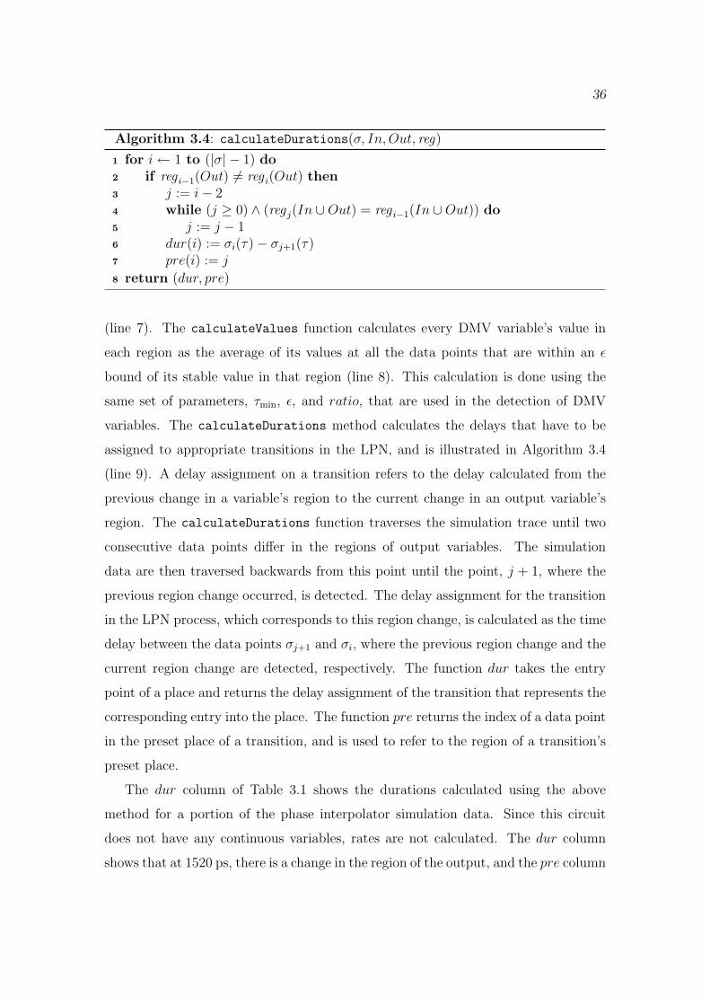
36
Algorithm 3.4: calculateDurations(σ, In,Out, reg)
for i← 1 to (|σ| − 1) do1
if reg i−1(Out) 6= reg i(Out) then2
j := i− 23
while (j ≥ 0) ∧ (reg j(In ∪Out) = reg i−1(In ∪Out)) do4
j := j − 15
dur(i) := σi(τ)− σj+1(τ)6
pre(i) := j7
return (dur, pre)8
(line 7). The calculateValues function calculates every DMV variable’s value in
each region as the average of its values at all the data points that are within an ǫ
bound of its stable value in that region (line 8). This calculation is done using the
same set of parameters, τmin, ǫ, and ratio, that are used in the detection of DMV
variables. The calculateDurations method calculates the delays that have to be
assigned to appropriate transitions in the LPN, and is illustrated in Algorithm 3.4
(line 9). A delay assignment on a transition refers to the delay calculated from the
previous change in a variable’s region to the current change in an output variable’s
region. The calculateDurations function traverses the simulation trace until two
consecutive data points differ in the regions of output variables. The simulation
data are then traversed backwards from this point until the point, j + 1, where the
previous region change occurred, is detected. The delay assignment for the transition
in the LPN process, which corresponds to this region change, is calculated as the time
delay between the data points σj+1 and σi, where the previous region change and the
current region change are detected, respectively. The function dur takes the entry
point of a place and returns the delay assignment of the transition that represents the
corresponding entry into the place. The function pre returns the index of a data point
in the preset place of a transition, and is used to refer to the region of a transition’s
preset place.
The dur column of Table 3.1 shows the durations calculated using the above
method for a portion of the phase interpolator simulation data. Since this circuit
does not have any continuous variables, rates are not calculated. The dur column
shows that at 1520 ps, there is a change in the region of the output, and the pre column

37
shows that the index of the last point prior to the region change that occurred before
this event is 6. Intuitively, there is a transition from region 000 to 101 with a delay
of 1380 ps which is obtained by taking the difference of 1520 and 140 ps. Similarly,
at 3900 ps, there is a transition from region 101 to 000 with a delay of 1760 ps.
The simulation traces provided by the designer often start at an arbitrary point
and end at another arbitrary point. The delay bounds on some of the transitions in
the generated LPN can vary widely depending on the point where the simulation trace
begins. To deal with this transient behavior that is observed due to indefinite start
points of the simulation traces, the addInitialTransient function adds a transient
place to the postset of the initial place, p0, for every simulation trace. The transition
between the initial place and the transient place sets the initial state as observed in the
corresponding simulation trace. The transient place corresponds to the starting region
of the simulation trace and a transition from this place takes the token to the actual
process constructed from the simulation trace. The construction of the actual process
starts at the data point that follows the transient region, and hence this function
returns that data point also. The addition of transient places in this way helps
separate undesired start-up conditions of the simulation trace from the functional
portion of the model. This method is explained in greater detail in Section 3.4.1.
If the process being generated has a nonempty set of control inputs, the func-
tion addStableToData determines the value of stable at each data point as 0 or
1 depending on whether the circuit is displaying transient behavior or steady-state
behavior, respectively, at that point (line 12). The parameter, tol , is the tolerance
allowed in the values, delays, and rates of the variables while in the steady-state and
is used to distinguish the transient behavior from steady-state behavior of the circuit.
The region assignments of the data points are then updated by including the variable,
stable. A detailed description of this method is given in Section 3.4.2. Since the region
assignments of the data points are changed, the rate, value, and delay assignments
are recalculated with the updated region assignments (lines 13-15).
The updateLPN function updates the LPN with the new places, transitions, and
assignments that result from the current simulation trace (line 16). While traversing
a simulation trace, whenever a variable v, which happens to be an input to the block

38
being modeled, crosses a threshold, th, to switch from region 1 to region 2, a transition
is added which connects places corresponding to regions 1 and 2 in the LPN. This
transition gets {v ≥ th} or {¬(v ≥ th)} as the enabling condition depending on the
direction in which the threshold is crossed. Thus, this condition is treated as a cause
for the event that follows. If the variable v, which is moving from region 1 to region 2,
is not an input to the block, then this action is treated as an effect and the preceding
change in the region is treated as a cause. If v is a DMV variable, then the duration
spent in region 1 is assigned to the delay, and the stable value in region 2 is assigned
to the DMV variable by the transition connecting the corresponding places in the
LPN. If v is a continuous variable, then the same transition would assign a rate to v
as opposed to the values and delays which are assigned for its DMV counterpart. The
LPN is then updated with the new places and transitions from the current simulation
trace. If a transition already exists, then the rate, value, and delay assignments are
updated by taking the union of the already existing ranges on the transition with
the new ones. A detailed description of this method is given in Section 3.5.1. The
updateLPN function also returns a region function that maps a place to a vector
formed by the region assignments, reg i(Care), of all the care variables in the place.
The region function returns the region assignment of a given variable in a given place.
Repeating the above steps for the remainder of the simulation traces from the given
set, Σ, produces an LPN process for the given component. Though the component
provided by the user does not have a stable variable, this LPN process has a stable
variable as an input. Since the testbench for the circuit is unaware of this variable,
it has to be driven internally within the model. To drive the stable variable, a new
component that has Ctl as the inputs, stable as the only output, Ctl as the set of care
variables, and no control inputs, is created. The genProcess function is called again
with this new component and the simulation traces, Σ, which are already updated
by the addStableToData function, to generate an LPN process that drives the stable
variable based on the control inputs of the circuit (lines 17-19). Thus, the process
previously generated for the circuit, which has stable as one of the inputs, behaves
accordingly.
39
The LPN model generated so far encapsulates the circuit behavior from all the
given simulations. However, this LPN model represents the actual circuit only for
the input sequences which are present in the simulations used for generating the
model. This model can potentially show unusual behavior like deadlocks when it
is subjected to a different input sequence. This problem does not exist if none of
the input variables is a care variable (i.e., Care 6= ∅). If the sequence of changes
of some of the inputs is important and they are selected as care variables, then,
the insertPseudoTransitions function inserts pseudo-transitions for the possible
region changes of those variables (line 20). Pseudo-transitions differ from the regular
transitions in that they are not observed in the given simulations and they serve
the purpose of taking the token in the LPN to an appropriate place based on the
applied inputs. A detailed explanation on how pseudo-transitions are added is given
in Section 3.5.2. At this point, the generation of the process in the LPN model which
corresponds to the given component is complete.
3.4 Dealing with Transient Behavior
Transient behavior is the response of a circuit that is observed for a short period of
time and is generally different from its steady-state behavior. It is important that an
abstract model of a circuit distinguishes its transient behavior from the steady-state
behavior. Without such distinction, the LPN models generated from simulation traces
can be very inaccurate and in some cases the models may be completely corrupted by
the transient behavior. This section describes the approaches for modeling two types
of transient behavior that can be present in the simulation traces. The first type,
called initial transient, is the transient behavior that is observed in the simulations
due to an indefinite start point and this behavior is not a property of the circuit. The
second type, called intermediate transient, is the conventional transient behavior that
is inherent in the circuits due to their nonzero response times to the stimuli applied.
3.4.1 Initial Transient
The model generation method described in Sections 3.2 and 3.3 requires the analog
designers to provide simulations of the circuit being modeled. Since the type of

40
simulation traces provided depends largely on the designer, the model generation
tool has to be robust enough to be able to accept a large range of simulation traces.
The simulation traces provided by the designer often start at an arbitrary point. For
instance, a trace which has a set of periodic signals rarely starts at a point where
all the signals are simultaneously transitioning from one period to another. In many
cases, such points may not exist in the simulations because the phase relationships of
the signals dictate their existence.
The simulation data shown in Table 2.1 do not start at the rising/falling edge of
phi. Instead, they start at a point somewhere in the period when phi is -2.5 V. So,
phi has a value of -2.5 V for that duration (140 ps) at the start of the simulation
and for 2000 ps throughout the rest of the simulation. So, it is important that
the tool distinguishes this situation from other situations where the duration for
which phi is 2.5 V changes between 140 ps and 2000 ps at different instances in
the simulation. If this distinction is not made, then the tool misinterprets that phi
can be at 2.5 V for a duration which can be anywhere between 140 ps and 2000 ps
throughout the simulation. So, the generated model has this duration as a randomly
chosen value between these extremes. But, in reality, this is not the case because
the 140 ps duration is only due to the simulation trace starting at that point, and it
does not exist in the clock generation circuitry. Thus, using such traces, where some
of the periodic signals are somewhere in between their periods at the start of the
trace, can potentially generate models which are very inaccurate. The large amount
of uncertainty in the delays makes the model overly conservative, leading to false
negative verification results.
To account for this inaccuracy, the addInitialTransient function adds a tran-
sient place that represents the starting region of the given simulation trace for a given
process in the LPN. The transient place transfers the token to the actual process upon
satisfying the enabling condition and waiting for the delay specified on its outgoing
transient transition. Algorithm 3.5 illustrates the method of adding initial transients.
The addPlace function on line 2 adds a place, p, to the LPN and returns the added
transient place. The getEnablingCond function takes the input variables, the region
assignment for the transition’s postset place, and the threshold values of the variables,

41
Algorithm 3.5: addInitialTransient(N, p0, σ, reg , c, dur, rate, val , θ)
let c = 〈In, Out, Care, Ctl〉1
(N, p) := addPlace(N)2
en := getEnablingCond(In, reg0, θ)3
N := addT(N, p0, p, en, 0, rate(0), val(0))4
for i← 1 to (|σ| − 1) do5
if reg i−1(Care) 6= reg i(Care) then6
(N, p′, region) := addPlace(N, reg i(Care), c, region)7
en := getEnablingCond(In, reg i, θ)8
N := addT(N, p, p′, en, dur(i), rate(i), val(i))9
break10
return (N, i)11
and returns the enabling condition of the transition (line 3). As the transient place
represents the starting region, which begins at data point 0, of a simulation trace,
reg0 is given as the region assignment of the postset place for a transition between
the initial place, p0, and the transient place, p. The addT function on line 4 adds a
transition between places p0 and p with an enabling condition en, a delay assignment
of 0, and the rate and value assignments calculated at the data point 0. In other words,
this transition sets the initial state of the LPN process when its enabling condition
evaluates to true. The simulation trace is then traversed until a point with a region
assignment that is different from that of the transient place is found (lines 5-6). The
addPlace function creates a place for the new region assignment and updates the
mapping in the region function for the new place (line 7). A transient transition is
added between the transient place, p, and the new place, p′, with the duration, rate,
and value assignments stored at the start point of the new region. This function
returns the LPN, N , updated with the above places and transitions and the index, i,
of the data point from where the regular updating of the LPN begins.
The delay on the transient transition depends only on the point where the sim-
ulation trace starts and not the behavior of the circuit. Thus, these initial transient
places help separate such undesired start-up conditions of the simulation trace from
the functional portion of the model. Fig. 3.2 shows the phase interpolator model with
transient places p0, p7, and p9. It can be seen that these transient places isolate the
start-up conditions of the simulations from the actual circuit behavior thus resulting

42
p9
p7
p8
t10
p3
<ct
l:=2>
[160
00]
t9
[160
00]
<phi:=
2.5>
[200
0]t1
3
<phi:=
-2.5
>
[200
0]t1
2
<phi:=
2.5>
[140
]t1
1
t4t5
{¬(p
hi≥
0)}
<om
ega:
=unifor
m(1
.9,2
)>
t7
[unifor
m(1
720,
1730
)]
{¬(p
hi≥
0)}
<om
ega:
=unifor
m(2
.4,2
.5)>
[unifor
m(1
260,
1300
)]
{(ct
l≥
2.5)∧
(phi≥
0)}
t8
[unifor
m(1
740,
1750
)]
t2{¬
(ctl≥
1.5)∧
(phi≥
0)} <om
ega:
=unifor
m(1
.9,2
)>
{¬(p
hi≥
0)}
[176
0][1
380]
[0]
[0]
{(ct
l≥
1.5)∧¬
(ctl≥
2.5)∧¬
(phi≥
0)}
t3t6
{(ct
l≥
2.5)∧¬
(phi≥
0)}
<om
ega:
=unifor
m(2
.4,2
.5)>
[unifor
m(1
320,
1360
)]
{(ct
l≥
1.5)∧¬
(ctl≥
2.5)∧
(phi≥
0)}
<om
ega:
=unifor
m(1
.9,2
)><
omeg
a:=
unifor
m(2
.4,2
.5)>p2
p11
t1
p1
p0
Init
ialva
lues
:
omeg
a:=
2phi:=
-2.5
ctl:=
1
p0
<ct
l:=3>
[138
0]<
omeg
a:=
unifor
m(2
.4,2
.5)>
{¬(c
tl≥
1.5)∧
(phi≥
0)}
t0
p4
p p6
p10
p11
p5
Fig
ure
3.2:
Phas
ein
terp
olat
orLP
Nw
ith
init
ialtr
ansi
ents
.
43
in a model that resembles the given simulation trace much more closely than without
them.
3.4.2 Intermediate Transient
While the initial transient behavior discussed above is a property of the simulations
and not that of the circuits, intermediate transient behavior is due to the circuit as
it changes its mode of operation. It is typical for an analog circuit to achieve its
steady-state response after a nonzero time delay. On a similar note, whenever the
mode of operation of a circuit is changed, it can possibly take a finite time before
stabilizing into the new operating mode. The behavior of the circuit during this time
duration can potentially be very different from that shown after stabilizing in the new
operating mode, depending on the type of the circuit. Though the term, ‘intermediate
transient’, is being used, it actually applies to all the transient behavior that can be
attributed to the circuit design, topology, etc. and not necessarily transient behavior
displayed only during mode switching. For instance, in a VCO simulation, though the
controlling voltage has a nonzero value initially, the VCO starts to oscillate only after
some time and it attains the frequency corresponding to the control voltage after some
more time. Even this type of transient behavior is being classified as intermediate
transient because it is due to the property of the circuit and not the simulation trace.
Depending on the level of accuracy desired, an abstract model for a circuit should
be able to capture both transient behavior and steady-state behavior. To serve
the purpose of functional validation, the model should certainly capture the correct
steady-state behavior whether or not it captures the transient behavior of the circuit.
The improved method for model generation addresses this concern by allowing for
detection of transient behavior based on the tolerance specification, tol . The inputs
of a circuit which when triggered cause the circuit to show a transient behavior that is
different from the steady-state behavior are called control inputs. The set of control
inputs to a circuit, Ctl, are assumed to be specified by the designer.
The addStableToData function assigns a Boolean value to the stable variable,
added by the addStableVariable function, at every data point in the simulation
trace, σ. The value of this state variable at each data point is determined to be either

44
0 or 1 using the user-specified tolerance parameter, tol . The tol parameter defines the
amount of variation that is allowed when a circuit has stabilized in a new operating
mode. Any variation beyond this tolerance, that is observed in the simulation, is
attributed to transient behavior. Thus, the state variable stable serves the purpose
of isolating the transient behavior from the steady-state behavior observed in the
simulations. The transient behavior in an LPN is displayed in the form of wider
ranges of delay assignments, value assignments, or rate assignments on the transitions
as compared to those in the steady-state.
Algorithm 3.6 illustrates the steps involved in the isolation of transient behavior
from the steady-state behavior in a simulation trace using the stable variable. Though
this algorithm determines the value of stable only based on the delays of the transi-
tions recorded in dur, it can easily be extended to determine the value of stable based
on the value and rate assignments of transitions. The simulation trace is traversed
until a region change occurs due to a threshold crossing of a control input (lines 6-7).
After this traversal, the start and end points for the portion of the simulation trace
where the value of ctl is constant are recorded in i and j, respectively. When the
delays on the transition are observed starting from this end point until the start point,
the delay on the first occurrence of a transition corresponds to the steady-state delay
on the transition, provided the simulation guarantees that a steady-state is achieved
for all the modes of operation (lines 9-12). The last function returns such steady-state
delay for every transition between two regions. The delays on the other occurrences of
the same transition are traversed until a delay is not within the tolerance specification
with respect to the steady-state delay (lines 13-15). The latest point where at least
one of the transition delays is not within the tolerance specification is stored in mark.
The points from the start point to mark have the value of stable as 0 and the points
from mark to end point have the value of stable as 1. As stable is a binary variable
with a single real threshold of 0.5, the region assignment of stable is always the same
as its value (lines 16-22). Thus, the value of stable for this particular portion of the
simulation trace indicates whether the delays on the transitions represent a transient
behavior or steady-state behavior. This process is repeated for the remaining portions
of the simulation trace that have a constant value for ctl.

45
Algorithm 3.6: addStableToData(σ, c, reg , dur, pre, par)
let c = 〈In, Out, Care, Ctl〉1
V ar = In ∪Out2
i := 03
do4
j := i + 15
while (j < |σ|) ∧ (reg i(Ctl) = reg j(Ctl)) do6
j := j + 17
last(∗, ∗) := undef8
for k ← (j − 1) downto (i + 1) do9
if regk(Out) 6= regk−1(Out) then10
if last(regpre(k)(V ar), regk(V ar)) = undef then11
last(regpre(k)(V ar), regk(V ar)) := dur(k)12
else if|last(regpre(k)(V ar),regk(V ar))−dur(k)|
last(regpre(k)(V ar),regk(V ar))> tol then
13
mark := k14
break15
for k ← (j − 1) downto i do16
if k ≥ mark then17
σk(stable) := 118
regk(stable) := 119
else20
σk(stable) := 021
regk(stable) := 022
i := j − 123
while i < (|σ| − 1 )24
return (σ, reg)25

46
To extend this algorithm to assign the values of stable based on the value and rate
assignments, the last function can store the values and the rates of variables, and the
same technique used for delays can be used to determine the points where the values
and rates are crossing the specified tolerance limits with respect to their steady-state
counterparts. At the end of this step, the value of stable is 1 for only those portions
of the simulation trace where the delays, values, and rates are within the tolerance
limits of their steady-state counterparts.
Fig. 3.3 shows the LPN model that is generated when the above method is applied
to the phase interpolator simulation. This LPN shows the result of only adding the
stable variable and does not show the initial transients for the sake of simplicity.
The transient behavior in this example is displayed in the form of phase delay of
the output and hence, stable is assigned values only based on the delay assignments
of the transitions. It can be seen that this LPN has two loops for every value of
ctl, one for transient (i.e., stable = 0) and the other for steady-state (i.e., stable =
1). Thus, the newly introduced state variable is used in this LPN to isolate the
transient period, during which the phase delay of the output is stabilizing to the
steady-state value of a particular operating mode, from the steady-state period. The
initial transient problem described in the previous section can also be solved by adding
an exclusive state variable which in turn creates a separate transient place, but it may
be unnecessary for simple initial transients.
3.5 Generalizing the Extracted LPN
The model generated from a set of circuit simulations is expected to represent
the circuit for at least the operating modes that are present in the given simulation
traces. For instance, in a phase interpolator, the value of ctl decides the phase offset
of the output omega with respect to the input phi. Thus, ctl is the signal that defines
the phase interpolator’s mode of operation. The simulation trace used to generate
the model shown in Fig. 3.1 had ctl switching monotonically from 1 to 3 in steps of 1.
Ideally, the generated model is supposed to be as good as the circuit is at least when
ctl holds a value from the set {1, 2, 3}. However, the LPN model shown in Fig. 3.1
represents the phase interpolator circuit for a very limited set of test configurations.
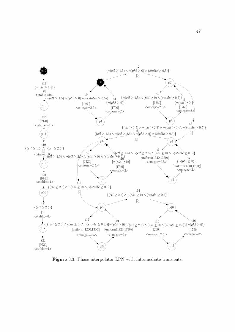
47
t17{¬(ctl ≥ 1.5)}
[0]
t18
<stable:=1>[9720]t22
<stable:=0>[0]
{(ctl ≥ 2.5)}
p9p0
t12
<omega:=2.5> <omega:=2>
[uniform(1720,1730)]
<omega:=2.5>
[1260]
{(ctl ≥ 2.5) ∧ ¬(phi ≥ 0) ∧ (stable ≥ 0.5)}t14
[0]
[0]
{(ctl ≥ 2.5) ∧ ¬(phi ≥ 0) ∧ ¬(stable ≥ 0.5)}
p7p0
p1p0
{¬(ctl ≥ 1.5) ∧ ¬(phi ≥ 0) ∧ (stable ≥ 0.5)}t2
[0]
{(ctl ≥ 2.5) ∧ (phi ≥ 0) ∧ ¬(stable ≥ 0.5)}
<stable:=1>[9740]
[1720]
{(ctl ≥ 2.5) ∧ (phi ≥ 0) ∧ (stable ≥ 0.5)}{¬(phi ≥ 0)}t16
<omega:=2>
<omega:=2>[1760]
t4
t3
[1380]
<omega:=2.5>
t0{¬(ctl ≥ 1.5) ∧ (phi ≥ 0) ∧ ¬(stable ≥ 0.5)}
[1380]<omega:=2.5>
<omega:=2>[1760]
{¬(phi ≥ 0)}t1
{¬(phi ≥ 0)}
[uniform(1260,1300)]
{¬(ctl ≥ 1.5) ∧ (phi ≥ 0) ∧ (stable ≥ 0.5)}
[0]
t5
{(ctl ≥ 1.5) ∧ ¬(ctl ≥ 2.5) ∧ ¬(phi ≥ 0) ∧ (stable ≥ 0.5)}
[0]
{(ctl ≥ 1.5) ∧ ¬(ctl ≥ 2.5) ∧ ¬(phi ≥ 0) ∧ ¬(stable ≥ 0.5)}t8
{¬(phi ≥ 0)}t7
<omega:=2>
{¬(phi ≥ 0)}
[1740]
t10
<omega:=2.5>
t6
[uniform(1320,1360)]<omega:=2.5>
{(ctl ≥ 1.5) ∧ ¬(ctl ≥ 2.5) ∧ (phi ≥ 0) ∧ ¬(stable ≥ 0.5)}t9
[1320]
[uniform(1740,1750)]<omega:=2>
<stable:=1>[3920]
{(ctl ≥ 1.5) ∧ ¬(ctl ≥ 2.5) ∧ (phi ≥ 0) ∧ (stable ≥ 0.5)}<stable:=0>
[0]{(ctl ≥ 1.5) ∧ ¬(ctl ≥ 2.5)}
p
p17
p10
p11p
p13
p14
p3p
p15
p16
p4
p12
p5
p2p0
t11
t19
t20
t21
p6
t15
p8
t13{¬(phi ≥ 0)}
<stable:=0>
Figure 3.3: Phase interpolator LPN with intermediate transients.
48
Transitions t2 and t5 are the only transitions that can change the mode of operation
of this model, which means that the only way in which the model can operate as if
ctl = 2 is by firing transition t2 and the only way to operate as if ctl = 3 is by firing
transition t3.
Effectively, this model just describes the simulation traces from which it is gener-
ated. Thus, it is functional only when the inputs change in the sequence that occurred
in the given simulation traces. The model’s behavior is not correct for any other input
sequence. In other words, this model shows a potential incorrect behavior even for
the input combinations that are present in the given simulation traces depending on
the sequence in which the inputs change in the simulation traces. For instance, if
the value of ctl is changed from 2 to 1 when the token is at place p2, then there is
no transition that can fire until ctl changes to 2 or 3, resulting in a deadlock. This
deadlock would not occur if the circuit’s simulation trace had a situation where ctl
changes from 2 to 1. Simulating an analog circuit for different modes of operation is
possible, but it is not feasible to exercise all possible permutations of the modes of
operation. So, the above problem cannot be solved by having extra simulations, and
it has to be addressed by a more general model generation method. Two methods are
presented here to generalize the LPN model such that it shows predictable behavior
for an arbitrary sequence of input changes. The first is a functional approach for
generating the models and the second approach is insertion of pseudo-transitions as
a post-processing step for model generation. The trade-offs of both the methods are
discussed and it is shown that the methods complement each other when they are
applied together.
3.5.1 Functional Approach
Each place in the LPN shown in Fig. 3.1 is a unique state formed by a combination
of the regions to which each variable belongs. For instance, place p0 represents the
portion of the simulation trace where the value of ctl is less than 1.5, the value of phi
is less than 0, and the value of omega is 2. Similarly, place p2 represents the portion of
the simulation trace where the value of ctl lies between 1.5 and 2.5, the value of phi is
less than 0, and the value of omega is 2. It can be observed that places p0 and p2 differ
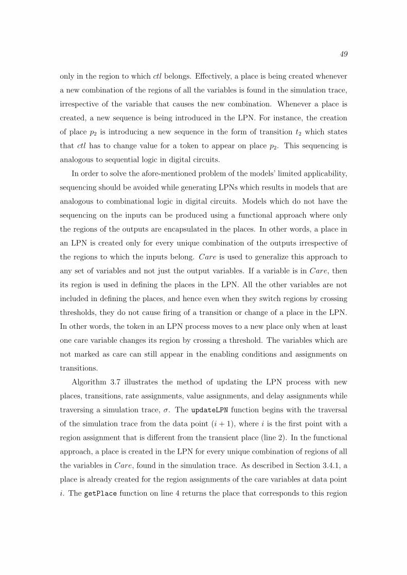
49
only in the region to which ctl belongs. Effectively, a place is being created whenever
a new combination of the regions of all the variables is found in the simulation trace,
irrespective of the variable that causes the new combination. Whenever a place is
created, a new sequence is being introduced in the LPN. For instance, the creation
of place p2 is introducing a new sequence in the form of transition t2 which states
that ctl has to change value for a token to appear on place p2. This sequencing is
analogous to sequential logic in digital circuits.
In order to solve the afore-mentioned problem of the models’ limited applicability,
sequencing should be avoided while generating LPNs which results in models that are
analogous to combinational logic in digital circuits. Models which do not have the
sequencing on the inputs can be produced using a functional approach where only
the regions of the outputs are encapsulated in the places. In other words, a place in
an LPN is created only for every unique combination of the outputs irrespective of
the regions to which the inputs belong. Care is used to generalize this approach to
any set of variables and not just the output variables. If a variable is in Care, then
its region is used in defining the places in the LPN. All the other variables are not
included in defining the places, and hence even when they switch regions by crossing
thresholds, they do not cause firing of a transition or change of a place in the LPN.
In other words, the token in an LPN process moves to a new place only when at least
one care variable changes its region by crossing a threshold. The variables which are
not marked as care can still appear in the enabling conditions and assignments on
transitions.
Algorithm 3.7 illustrates the method of updating the LPN process with new
places, transitions, rate assignments, value assignments, and delay assignments while
traversing a simulation trace, σ. The updateLPN function begins with the traversal
of the simulation trace from the data point (i + 1), where i is the first point with a
region assignment that is different from the transient place (line 2). In the functional
approach, a place is created in the LPN for every unique combination of regions of all
the variables in Care, found in the simulation trace. As described in Section 3.4.1, a
place is already created for the region assignments of the care variables at data point
i. The getPlace function on line 4 returns the place that corresponds to this region
50
Algorithm 3.7: updateLPN(N, σ, i, reg , c, dur, pre, rate, val , θ)
let c = 〈In, Out, Care, Ctl〉1
for j ← (i + 1) to (|σ| − 1) do2
if reg j−1(Care) 6= reg j(Care) then3
p := getPlace(N, reg j−1, c)4
(N, p′, region) := addPlace(N, reg j(Care), c, region)5
if (reg j−1(Out) 6= reg j(Out)) ∧ (regpre(j)(In) 6= reg j−1(In)) then6
en := getEnablingCond(In, reg j, θ)7
p′′ := getPlace(N, regpre(j), c)8
N := addT(N, p′′, p′, en, dur(j), rate(j), val(j))9
enPrev := getEnablingCond(In, reg j−1, θ)10
N := removeT(N, p′′, p, enPrev)11
if •p = ∅ then12
N := removeP(N, p)13
else if (reg j−1(Out) 6= reg j(Out)) then14
en := true15
N := addT(N, p, p′, en, dur(j), rate(j), val(j))16
else17
en := getEnablingCond(In, reg j, θ)18
N := addT(N, p, p′, en, 0, rate(j), val(j))19
N := mergeTransitions(N)20
return (N, region)21
assignment. When a data point j is found to have a different region assignment, the
addPlace function creates a place corresponding to the new region and updates the
mapping for this place in the region function (lines 3-5). The addPlace function does
not add a new place if a place with the given region assignment already exists.
The next step is to add a transition between the two places. In contrast to places
which are identified just by the regions of care variables (i.e., reg i(Care)), transitions
are identified by the regions of all the variables (i.e., reg i(V )) in the preset and postset
places. The getEnablingCond function returns the enabling condition for a transition
based on the region assignments of the input variables in its postset place. The addT
function creates a new transition if a transition does not exist between the given preset
and postset places with the given enabling condition, and updates the transition with
the new assignments if it already exists. When a new rate, value, or delay is added
to a transition, the existing ranges on rates, values, or delays are updated to include

51
the new ones as described in [22]. Addition of transitions is done in 3 different ways
based on the type of variables whose region changes are represented by the transition
being added. The first is a transition that represents a region change in an output
that is following a previous region change in an input (line 6). The difference in the
region assignments reg j−1(Out) and reg j(Out) represents the current region change
in an output and the difference in the region assignments regpre(j)(In) and reg j−1(In)
represents the previous region change in an input. In this case, a transition is added
between the places p′′ and p′, which correspond to the regions regpre(j)(Care) and
reg j(Care), respectively (lines 7-9). The transition which may have been created
previously between the places p′′ and p, that represents the regions regpre(j)(Care)
and reg j−1(Care) respectively, is deleted by the removeT function (lines 10-11). If
this deleted transition is the only transition that can transport a token to place p,
then the place p is also deleted by the removeP function (lines 12-13). The second
case is a transition representing a region change on an an output but not following
a region change on an input (line 14). In this case, a transition between p and p′
that represents the current region change on the output is added. The enabling
condition of this transition is set to true because an immediate cause could not be
identified (line 15). This transition has delay, rate, and value assignments which are
precalculated and stored at the entry point of postset place, p′ (line 16). The third
case is a transition representing a region change on an input. A transition is added
between places p and p′ with an enabling condition representing the input region
change and a delay assignment of 0 because there is no region change on an output
DMV variable (lines 17-19).
Fig. 3.4 illustrates the process of adding a transition in an LPN using a portion
of the data shown in Table 3.1. It can be observed from the table that the value
of phi changes from -2.5 V to 2.5 V at 140 ps, thus crossing a threshold of 0 V.
When this data point is encountered while the updateLPN function is traversing the
simulation trace, the change in region results in the addition of transition t1 as shown
in Fig. 3.4a. At 1520 ps, when the output, omega, crosses a threshold of 2.016 V, it
is detected as a change in the region of an output that is following a change in the
region of an input. Hence, transition t2 with an enabling condition corresponding to
52
p
p”
[0]
t1
{(phi ≥ 0)&¬(ctl ≥ 1.5)}
(a)
p
[1380]
[0]
{(phi ≥ 0)&¬(ctl ≥ 1.5)}t1
t2
{(phi ≥ 0)&¬(ctl ≥ 1.5)}
< omega:=uniform(2.4,2.5)>
p’p”
(b)
t2
< omega:=uniform(2.4,2.5)>
[1380]
{(phi ≥ 0)&¬(ctl ≥ 1.5)}
p’
p”
(c)
Figure 3.4: Example illustrating the addition of a transition to an LPN. (a)Transition t1 added when a change in region of an input is detected. (b) Transitiont2 added when the change in region of an input is followed by a change in region ofan output. (c) Transition t1 deleted because it is included in t2.
the input region change at 140 ps, value assignments corresponding to the current
region change at 1520 ps, and a delay assignment of 1380 ps that corresponds to the
time difference of these two region changes, is added as shown in Fig. 3.4b. Since the
region change represented by t1 is embedded as an enabling condition in t2, transition
t1 is deleted. After deleting t1, place p has no preset transition, and hence is deleted
as well. Fig. 3.4c shows the resultant LPN after deleting the transition and place.
The LPN places, transitions, and labels are thus updated by traversing until the
end of the simulation trace. After updating the LPN process with new places and
transitions, it is simplified by invoking the mergeTransitions function presented in
Algorithm 3.8. This function finds a set of transitions which have the same preset and
postset places and the same value and rate assignments, and merges them into a single
transition with a new delay assignment and enabling condition (lines 3-5). The delay
assignment of each new transition is obtained by predicating the delay assignments of
all the merged transitions with their respective enabling conditions and taking their
sum (line 7). This operation ensures that an appropriate delay is chosen based on the
enabling condition that evaluates to true. The new transition’s enabling condition
is obtained by performing an OR operation on the individual transitions’ enabling
conditions (line 8). This operation ensures that the new transition is enabled when
53
Algorithm 3.8: mergeTransitions(N)
forall t1 ∈ T do1
Tmerge := ∅2
forall t2 ∈ (T − {t1}) do3
if (•t1 = •t2) ∧ (t1• = t2•)∧ assignmentsEqual(N, t1, t2) then4
Tmerge := Tmerge ∪ {t2}5
forall t ∈ Tmerge do6
d(t1) := d(t1) + d(t) ∗ En(t)7
En(t1) := En(t1) ∨ En(t)8
N := removeT(N, t)9
return N10
any of the merged transitions is enabled. Finally, all the transitions involved in the
merge operation are deleted using the removeT function (line 9).
An example for merging transitions is shown in Figure 3.5. In Figure 3.5a, it can
be observed that transitions t0 and t2 have the same preset and postset places, and
the same set of assignments. Consequently, the mergeTransitions function merges
these two transitions into a single transition, t0, as shown in Figure 3.5b.
Fig. 3.6 shows the LPN model of the phase interpolator with only the output
omega marked as a care variable. The steps that deal with the initial transient and
the intermediate transients have been bypassed while generating this LPN process
for the sake of simplicity. There are only two places, p0 and p1, in this LPN which
represent the regions where omega = 2 and omega = 2.5, respectively. In each of
these places, the regions of the variables which are not marked as care, ctl and phi,
can be anything. This fact implies that the ordering of the changes in regions of
any of these noncare variables is not maintained in this model. Though this LPN is
generated from the same simualtion trace that is used to generate the LPN in Fig. 3.1,
it does not encapsulate the order in which ctl and phi changed their values in the
simulation traces. This ability of the functional approach to disregard the order of
changes on the noncare variables makes the models more general in a way that they
can be simulated in a wider variety of test scenarios. The example LPN shown in
Fig. 3.6 can be simulated for any test-case as long as it has only those values of ctl

54
[unifor
m(1
00,2
00)]
[unifor
m(1
000,
2000
)]
{(in
=2)}
t2t0
{(in
=0)}
[unifor
m(1
0,20
)]
<ou
t:=
1>
{(in
=1)}
t1
<ou
t:=
0>
p0 p1
p1
<ou
t:=
1>
(a)
Tra
nsi
tions
bef
ore
mer
gin
g. p1 p1p0
t1{(
in=
1)}
[unifor
m(1
00,2
00)]
<ou
t:=
0>
<ou
t:=
1>
{(in
=0)|(in
=2)}
t0
[unifor
m((
in=
0)*1
0+(i
n=
2)*1
000,
(in=
0)*2
0+(i
n=
2)*2
000)
]
(b)
Tra
nsi
tions
aft
erm
ergin
g.
Fig
ure
3.5:
Exam
ple
illu
stra
ting
themergeTransitions
oper
atio
n.

55
Initial values:
phi:=-2.5ctl:=1
omega:=2p0
p1p0
[(¬(ctl ≥ 1.5) ∧ ¬(phi ≥ 0))*1760+
uniform(((ctl ≥ 2.5) ∧ ¬(phi ≥ 0))*1720,((ctl ≥ 2.5) ∧ ¬(phi ≥ 0))*1730)]
t1{¬(phi ≥ 0)}
<omega:=uniform(1.9,2)>
uniform(((ctl ≥ 1.5) ∧ ¬(ctl ≥ 2.5) ∧ ¬(phi ≥ 0))*1740,((ctl ≥ 1.5) ∧ ¬(ctl ≥ 2.5) ∧ ¬(phi ≥ 0))*1750)+
<omega:=uniform(2.4,2.5)>((ctl ≥ 2.5) ∧ (phi ≥ 0))*1300)]
((ctl ≥ 1.5) ∧ ¬(ctl ≥ 2.5) ∧ (phi ≥ 0))*1360)+uniform(((ctl ≥ 2.5) ∧ (phi ≥ 0))*1260,
uniform(((ctl ≥ 1.5) ∧ ¬(ctl ≥ 2.5) ∧ (phi ≥ 0))*1320,[(¬(ctl ≥ 1.5) ∧ (phi ≥ 0))*1380+
{(phi ≥ 0)}t0
Figure 3.6: Phase interpolator LPN generated using a functional approach.
and phi that are present in the original simulation trace irrespective of the order in
which they change.
3.5.2 Pseudo-Transitions
Insertion of pseudo-transitions is a straightforward way of dealing with the lim-
ited applicability problem of the LPNs generated from simulation traces. Pseudo-
transitions differ from the regular transitions in that they are not observed in the
given set of simulation traces. If the model shown in Fig. 3.1 is subjected to a
stimulus in which the value of ctl is changed from 2 to 1, then the model deadlocks.
Place p2 in this LPN corresponds to the region where the value of ctl lies between 1.5
and 2.5. When the value of ctl is changed to 1, the token in the LPN has to be forced
to an appropriate place which represents the new value of ctl. This functionality is
accomplished by the insertion of a pseudo-transition from p2 to p0 with an enabling
condition ¬(ctl ≥ 1.5).
Pseudo-transitions are not observed in the given simulation traces and they are
added to force the token in the LPN to be present in an appropriate region based
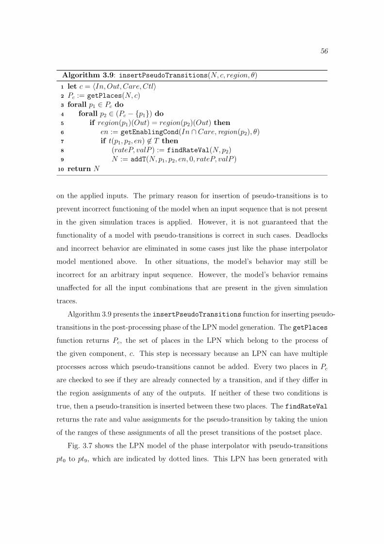
56
Algorithm 3.9: insertPseudoTransitions(N, c, region, θ)
let c = 〈In, Out, Care, Ctl〉1
Pc := getPlaces(N, c)2
forall p1 ∈ Pc do3
forall p2 ∈ (Pc − {p1}) do4
if region(p1)(Out) = region(p2)(Out) then5
en := getEnablingCond(In ∩ Care, region(p2), θ)6
if t(p1, p2, en) 6∈ T then7
(rateP, valP ) := findRateVal(N, p2)8
N := addT(N, p1, p2, en, 0, rateP, valP )9
return N10
on the applied inputs. The primary reason for insertion of pseudo-transitions is to
prevent incorrect functioning of the model when an input sequence that is not present
in the given simulation traces is applied. However, it is not guaranteed that the
functionality of a model with pseudo-transitions is correct in such cases. Deadlocks
and incorrect behavior are eliminated in some cases just like the phase interpolator
model mentioned above. In other situations, the model’s behavior may still be
incorrect for an arbitrary input sequence. However, the model’s behavior remains
unaffected for all the input combinations that are present in the given simulation
traces.
Algorithm 3.9 presents the insertPseudoTransitions function for inserting pseudo-
transitions in the post-processing phase of the LPN model generation. The getPlaces
function returns Pc, the set of places in the LPN which belong to the process of
the given component, c. This step is necessary because an LPN can have multiple
processes across which pseudo-transitions cannot be added. Every two places in Pc
are checked to see if they are already connected by a transition, and if they differ in
the region assignments of any of the outputs. If neither of these two conditions is
true, then a pseudo-transition is inserted between these two places. The findRateVal
returns the rate and value assignments for the pseudo-transition by taking the union
of the ranges of these assignments of all the preset transitions of the postset place.
Fig. 3.7 shows the LPN model of the phase interpolator with pseudo-transitions
pt0 to pt9, which are indicated by dotted lines. This LPN has been generated with
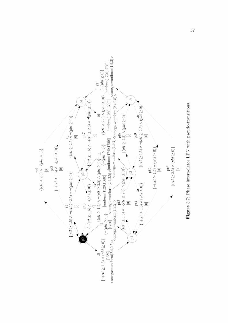
57
pt8
p2
t3t4
{¬(p
hi≥
0)}
<om
ega:
=unifor
m(1
.9,2
)>
t6
<om
ega:
=unifor
m(1
.9,2
)>[u
nifor
m(1
720,
1730
)]
{¬(p
hi≥
0)}
<om
ega:
=unifor
m(2
.4,2
.5)>
[unifor
m(1
260,
1300
)]
{(ct
l≥
2.5)∧
(phi≥
0)}
t7
[unifor
m(1
740,
1750
)]
t0{¬
(ctl≥
1.5)∧
(phi≥
0)} <om
ega:
=unifor
m(1
.9,2
)><
omeg
a:=
unifor
m(2
.4,2
.5)>
t1{¬
(phi≥
0)}
[176
0][1
380]
<om
ega:
=unifor
m(2
.4,2
.5)>
[unifor
m(1
320,
1360
)]
{(ct
l≥
1.5)∧¬
(ctl≥
2.5)∧
(phi≥
0)}
p
[0]
{(ct
l≥
2.5)∧
(phi≥
0)}
pt6
{¬(c
tl≥
1.5)∧
(phi≥
0)}
pt5 [0]
p4
{¬(c
tl≥
1.5)∧
(phi≥
0)}
{(ct
l≥
1.5)∧¬
(ctl≥
2.5)∧
(phi≥
0)}
p p3
{(ct
l≥
1.5)∧¬
(ctl≥
2.5)∧¬
(phi≥
0)}
{¬(c
tl≥
1.5)∧¬
(phi≥
0)}
{(ct
l≥
2.5)∧¬
(phi≥
0)}
[0]
pt1
{¬(c
tl≥
1.5)∧¬
(phi≥
0)}
[0]
pt2
{(ct
l≥
2.5)∧¬
(phi≥
0)}
t5 [0]
[0]
{(ct
l≥
1.5)∧¬
(ctl≥
2.5)∧¬
(phi≥
0)}
pt0 [0]
pt7 [0]
t2
{(ct
l≥
1.5)∧¬
(ctl≥
2.5)∧
(phi≥
0)}
{(ct
l≥
2.5)∧
(phi≥
0)}
pt9 [0]
pt4 [0]
pt3 [0]
[0]
p0 p1
p0
p5
Fig
ure
3.7:
Phas
ein
terp
olat
orLP
Nw
ith
pse
udo-
tran
siti
ons.
58
all the variables as care variables (i.e., Care = V ) and none of the inputs as control
variables (i.e., Ctl = ∅). The insertion of initial transient is also bypassed so that
only the effect of the insertion of pseudo-transitions can be seen in this model. It can
be seen that these pseudo-transitions aid the model in transporting the token to an
appropriate place when the inputs change in an arbitrary order that is not present in
the given simulations. By transporting the token to an appropriate place, the model
is being forced to represent the correct behavior, which in this case is the output’s
phase delay, based on the applied input, which is ctl in this example.
3.5.3 Limitations
The functional approach with only outputs as care variables is a good solution
only when the sequence in which inputs change is not an important criterion for the
circuit. For instance, the model shown in Fig. 3.6 does not distinguish whether the
delay assignments on the transitions are with respect to a change in the value of ctl
or phi. In other words, the delays shown on the transitions are phase delays with
respect to phi only if the test-bench is guaranteed to change the value of ctl before
the value of phi is changed. So, the reference with which the delay on the transition
is measured depends solely on the test-bench.
From the LPN shown in Fig. 3.7, it is evident that the number of pseudo-transitions
grows exponentially with the size of the model. As the number of pseudo-transitions
increases, the model’s complexity increases, thus complicating the analysis. Thus,
insertion of pseudo-transitions alone may not be a feasible solution for circuits with
more than a couple of inputs. The advantage of pseudo-transitions over the func-
tional approach is that models with pseudo-transitions preserve the sequence of input
changes in the model. Hence, there is a trade-off between the two methods involving
pseudo-transitions and the functional approach. Depending on the circuit and the
type of test environment that is used, a combination of the functional approach and
pseudo-transitions can be used to produce the desired model. Such a model can be
obtained by including the set of variables whose sequence of changes is important
in Care and inserting pseudo-transitions based on the region changes of these care
variables.

59
3.6 Conversion to SystemVerilog
Extracting the behavioral models in the form of LPNs alone is not sufficient
because they cannot be integrated with the industrial designs for simulation pur-
poses. So, the extracted LPN models should be represented in an industry-standard
hardware modeling language. In [22], the notion of representing LPNs in Verilog-
AMS and VHDL-AMS is introduced but a generic method for converting LPNs to
HDLs is not provided. Also, the presented Verilog-AMS and VHDL-AMS models do
not maintain the exact semantics of the LPNs. Verilog-AMS models are simulated
using mixed-signal simulators which typically have a continuous-time kernel and a
discrete-event kernel. The portion of the model in the analog block runs on the
continuous-time kernel and the rest of the model runs on the discrete-event kernel.
Though these abstract models simulate faster as compared to SPICE, the improvement
in performance is limited by the amount of code in the analog block [36]. To achieve
performance that is comparable to digital circuit simulations, it is important for
the LPN models to be represented in a language that can be simulated using a
discrete-event kernel alone. SystemVerilog is one such language as it allows the
flexibility to have real-valued signals on the ports of the modules [2]. Real-valued
ports are useful in modeling the continuously varying signals of analog circuits. Since
the simulator is event-based, the continuous variables are updated at small discrete
time intervals by using a clock which is sufficiently fast. The clock frequency can be
chosen based on the desired accuracy level.
The method for converting an LPN process to a SystemVerilog module involves
the following steps :
1. Add input and output ports.
2. Add procedural assignments for places in the initial block.
3. Add continuous assignments for transitions.
4. Add an always block for each transition in the LPN.
5. Add procedural assignments for places and variables in each transition’s always
block.

60
6. Add assertions.
The first step is to create real-valued input and output ports to the SystemVerilog
module. There are two types of assignments in Verilog — continuous assignments and
procedural assignments. A continuous assign statement evaluates the expression on
the right hand side whenever there is a change on any of the variables of the expression.
A procedural assignment is executed only when its container block is triggered.
Procedural assignments are present in initial and always blocks. All the places and
transitions in the LPN are represented as Boolean variables. The Boolean variables
representing transitions are assigned values using continuous assign statements and
those representing places are assigned values using procedural assignments in the
always block.
The initial marking of the LPN process is converted to an initial block in Sys-
temVerilog. In the initial block, a value of 0 is assigned to all the Boolean variables
representing places which are not initially marked in the LPN, and a value of 1 is
assigned to places which are initially marked. The initially marked places in the LPN
are assigned a value of 1 only after a nominal transport delay of one time unit, so that
there is a change in their values after the simulation starts, which causes events on the
transitions. Continuous assign statements are used to assign values to the Boolean
variables representing the transitions because the delays specified with continuous
assign statements are inertial delays which are in accordance with the semantics of
LPN transitions. The assign statements are created such that a Boolean variable
corresponding to a transition, t, is set to true after waiting for a delay returned by the
delay function when all the Boolean variables representing the places in its preset,
•t, evaluate to true and the enabling condition evaluates to true, indicating that the
transition is enabled.
Fig. 3.8 shows the delay function. If a transition is disabled at the instant it is
invoked, it adds a small random delay to the delay assignment on the transition and
returns this value. The addition of a small delay reduces the likelihood of simultaneous
firing of transitions, the semantics of which are not well-defined in SystemVerilog. If
a transition is enabled at the instant the delay function is invoked, it returns 0 as
the delay. In other words, this function ensures that enabling a transition requires
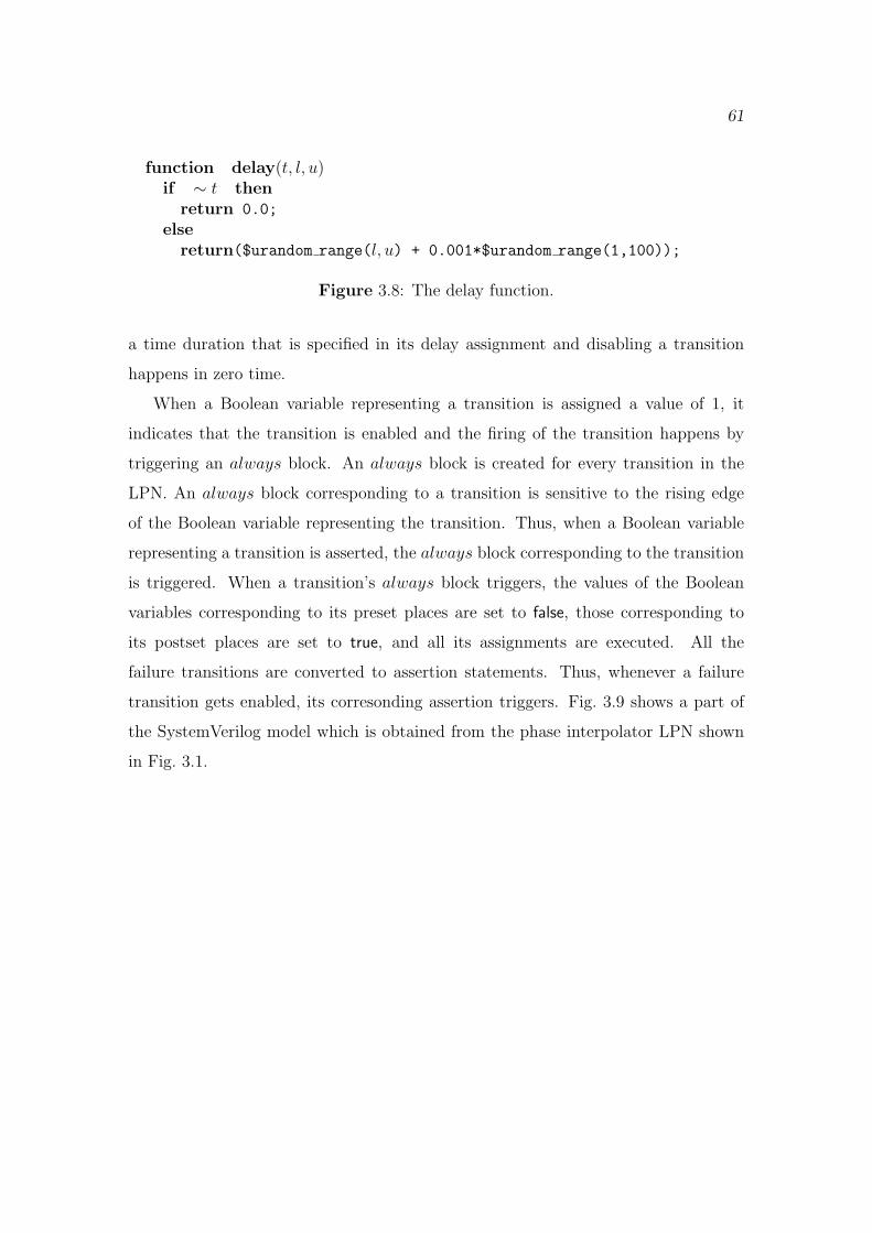
61
function delay(t, l, u)if ∼ t then
return 0.0;
elsereturn($urandom range(l, u) + 0.001*$urandom range(1,100));
Figure 3.8: The delay function.
a time duration that is specified in its delay assignment and disabling a transition
happens in zero time.
When a Boolean variable representing a transition is assigned a value of 1, it
indicates that the transition is enabled and the firing of the transition happens by
triggering an always block. An always block is created for every transition in the
LPN. An always block corresponding to a transition is sensitive to the rising edge
of the Boolean variable representing the transition. Thus, when a Boolean variable
representing a transition is asserted, the always block corresponding to the transition
is triggered. When a transition’s always block triggers, the values of the Boolean
variables corresponding to its preset places are set to false, those corresponding to
its postset places are set to true, and all its assignments are executed. All the
failure transitions are converted to assertion statements. Thus, whenever a failure
transition gets enabled, its corresonding assertion triggers. Fig. 3.9 shows a part of
the SystemVerilog model which is obtained from the phase interpolator LPN shown
in Fig. 3.1.
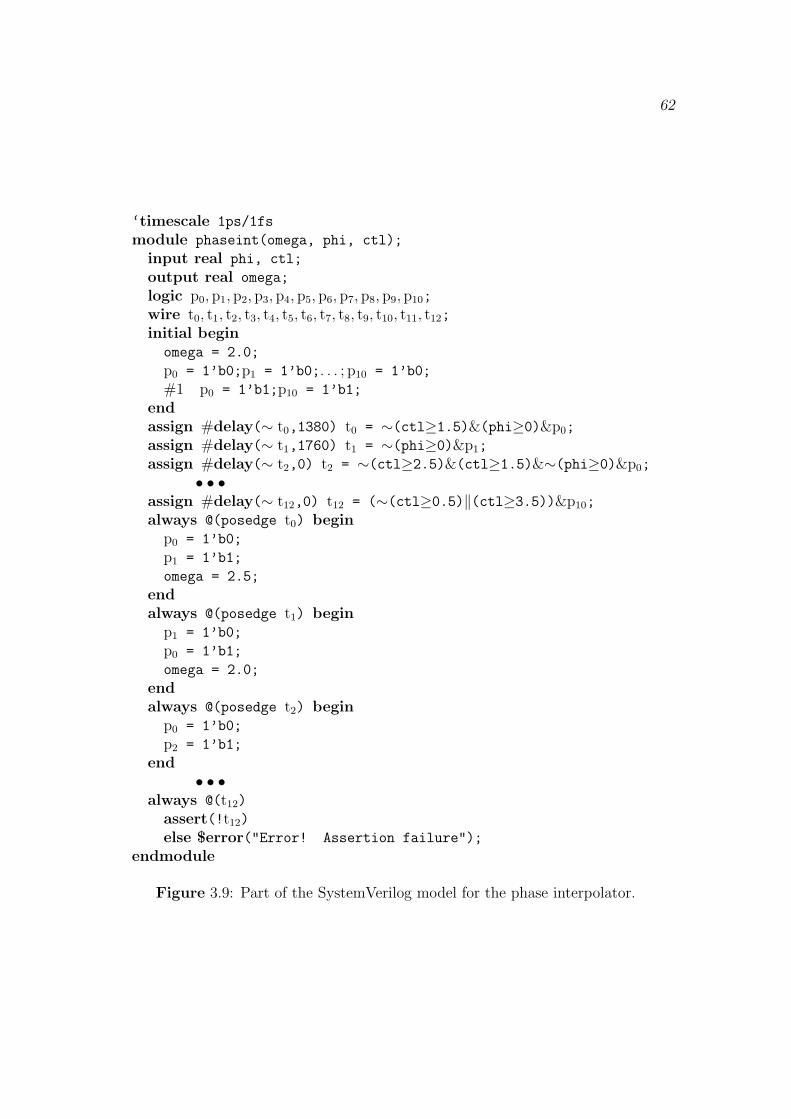
62
‘timescale 1ps/1fs
module phaseint(omega, phi, ctl);
input real phi, ctl;
output real omega;
logic p0, p1, p2, p3, p4, p5, p6, p7, p8, p9, p10;
wire t0, t1, t2, t3, t4, t5, t6, t7, t8, t9, t10, t11, t12;
initial beginomega = 2.0;
p0 = 1’b0;p1 = 1’b0;. . . ; p10 = 1’b0;
#1 p0 = 1’b1;p10 = 1’b1;
endassign #delay(∼ t0,1380) t0 = ∼(ctl≥1.5)&(phi≥0)&p0;
assign #delay(∼ t1,1760) t1 = ∼(phi≥0)&p1;
assign #delay(∼ t2,0) t2 = ∼(ctl≥2.5)&(ctl≥1.5)&∼(phi≥0)&p0;
• • •assign #delay(∼ t12,0) t12 = (∼(ctl≥0.5)‖(ctl≥3.5))&p10;
always @(posedge t0) beginp0 = 1’b0;
p1 = 1’b1;
omega = 2.5;
endalways @(posedge t1) begin
p1 = 1’b0;
p0 = 1’b1;
omega = 2.0;
endalways @(posedge t2) begin
p0 = 1’b0;
p2 = 1’b1;
end• • •
always @(t12)
assert(!t12)
else $error("Error! Assertion failure");
endmodule
Figure 3.9: Part of the SystemVerilog model for the phase interpolator.
CHAPTER 4
CASE STUDIES
This chapter presents two industrial-scale examples — a phase interpolator and
a VCO — on which the model generation method discussed in Chapter 3 has been
applied. For each of these examples, a circuit is designed at transistor-level, and the
circuit simulations are given to the LEMA tool for generating LPN and SystemVerilog
models. The models generated using various approaches, their advantages, and
limitations are discussed. The SystemVerilog models that are generated from the
LPNs, and their simulation results are shown.
4.1 Phase Interpolator
The phase interpolator models presented in Chapter 3 are generated from a simu-
lation that exercises only three values of ctl. However, the actual phase interpolator
circuit that is being modeled is capable of producing 16 phase divisions between the
two clocks, phi and psi. Thus, the models shown previously are not complete, and
they only display the partial behavior of the circuit. So, a simulation has to exercise
all 16 values of ctl to produce a behavioral model that can be used to replicate
the circuit’s functionality. Fig. 4.1 shows the LPN model that is generated from a
simulation trace in which the design is simulated for all the values of ctl. In this model,
only the output, omega, is a care variable, and hence the LPN has two places, p1 and
p2, corresponding to the two regions of omega, and an initial transient place, p0. This
model does not have the internal state variable, stable, because this circuit simulation
does not display transient behavior for a significant amount of time. Hence, none of
the input variables is specified as a control variable, resulting in a model without the
stable variable.
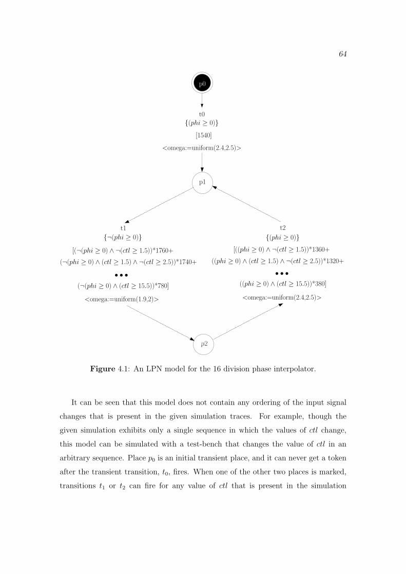
64
((phi ≥ 0) ∧ (ctl ≥ 1.5) ∧ ¬(ctl ≥ 2.5))*1320+
[((phi ≥ 0) ∧ ¬(ctl ≥ 1.5))*1360+
<omega:=uniform(1.9,2)>
(¬(phi ≥ 0) ∧ (ctl ≥ 15.5))*780]
• • •
[(¬(phi ≥ 0) ∧ ¬(ctl ≥ 1.5))*1760+
{¬(phi ≥ 0)} {(phi ≥ 0)}
t0{(phi ≥ 0)}
[1540]
p0
(¬(phi ≥ 0) ∧ (ctl ≥ 1.5) ∧ ¬(ctl ≥ 2.5))*1740+
p2p0
t2t1
p1
<omega:=uniform(2.4,2.5)>
<omega:=uniform(2.4,2.5)>
((phi ≥ 0) ∧ (ctl ≥ 15.5))*380]
• • •
Figure 4.1: An LPN model for the 16 division phase interpolator.
It can be seen that this model does not contain any ordering of the input signal
changes that is present in the given simulation traces. For example, though the
given simulation exhibits only a single sequence in which the values of ctl change,
this model can be simulated with a test-bench that changes the value of ctl in an
arbitrary sequence. Place p0 is an initial transient place, and it can never get a token
after the transient transition, t0, fires. When one of the other two places is marked,
transitions t1 or t2 can fire for any value of ctl that is present in the simulation

65
trace irrespective of the sequence in which the variables change values and the delay
expression on the transition makes sure that an appropriate delay is chosen based on
the input values. This model demonstrates that the functional approach prevents the
occurrence of deadlocks and unexpected behavior.
Fig. 4.2 shows a property LPN that is used to verify the functionality of a phase
interpolator. This LPN verifies that a change in the interpolation control bits effect
a corresponding change in the phase of the output clock, omega, with respect to the
input clock, phi. In the initial state, transition tClk fires as soon as the value of phi
crosses 0 V. Places pChkMin and pChkMax each attain a token when transition tClk
fires. Based on the value of ctl, one of the tMinN transitions fires after a minimum
delay that is specified on the transition, and a token appears on the place pChk. If the
value of omega crosses 2.2 V before this minimum delay, then the tFailMin transition
fires thus terminating the simulation. Similarly, one of the tMaxN transitions fires
after a maximum delay specified on a transition with the appropriate value of ctl in
the enabling condition. The tMax transitions, being failure transitions, terminate the
simulation when the phase delay of omega is greater than the maximum allowed delay
for a particular value of ctl. If omega crosses 2.2 V before the maximum specified
delay, and if pChk has a token, then transition tChk fires, and a token appears on
place pRst. This LPN checks the phase delay only for the rising edge of the output
clock, and hence there is no phase delay check after the input clock, phi, goes below
0 V. The above logic can be replicated after the value of phi goes below 0 V to
verify the phase delay for a falling edge. LPN models that are generated using the
simulations of phase interpolators with 4 divisions, 8 divisions, and 16 divisions have
been verified with property LPNs similar to Fig. 4.2. Table 4.1 presents the results for
these examples when verified with LEMA’s model checker [37]. Though this property
looks simple, it exposed a number of problems in the model generator.
Fig. 4.3 shows the SystemVerilog model that is obtained from the LPN shown
in Fig. 4.1. Here, the inertial delays of the continuous assignment statements are
a function of the values of ctl and phi. This dependence of delay on ctl and phi
demonstrates the phase interpolation operation. In other words, when there is an
event on the expression on the right hand side of the assign statement, the values of
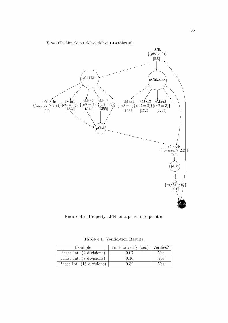
66
... ...
[0,0]
tClk{(phi ≥ 0)}
pRst
pChkMaxpChkMin
tMin2
[1355]
tMin1
[1315]{(ctl = 2)}{(ctl = 1)}
tMin3
{(ctl = 3)}[1265]
tMax2tMax1 tMax3{(ctl = 2)}
[1325][1365]
{(ctl = 3)} {(ctl = 1)}tFailMin
{(omega ≥ 2.2)}
[0,0][1255]
tCheck
[0,0]{(omega ≥ 2.2)}
pClk
{¬(phi ≥ 0)}tRst
[0,0]
Tf := {tFailMin,tMax1,tMax2,tMax3,• • •,tMax16}
pChk
Figure 4.2: Property LPN for a phase interpolator.
Table 4.1: Verification Results.
Example Time to verify (sec) Verifies?Phase Int. (4 divisions) 0.07 YesPhase Int. (8 divisions) 0.16 YesPhase Int. (16 divisions) 0.32 Yes

67
‘timescale 1ps/1fs
module pi16(omega, phi, ctl);
input real phi, ctl;
output real omega;
wire t0, t1, t2;
logic p0, p1, p2;
initial beginp0 = 0; p1 = 0; p2 = 0;#1 p0 = 1; //Initially Marked
endassign #(delay(∼ t0,1540)) t0 = p0 && (phi≥0);assign #delay(∼ t1,(!(phi≥0)&&!(ctl≥1.5))*1760+
(!(phi≥0)&&(ctl≥1.5)&&!(ctl≥2.5))*1740+• • •
(!(phi≥0)&&(ctl≥15.5))*780)t1 = p1 && !(phi≥0);
assign #delay (∼ t2,(!(ctl≥1.5)&&(phi≥0))*1360+((ctl≥1.5)&&!(ctl≥2.5)&&(phi≥0))*1320+
• • •((ctl≥15.5)&&(phi≥0))*380)
t2 = p2 && (phi≥0);always @(posedge t0) begin
p0 = 0; p1 = 1; omega = uniform(2.4,2.5);
endalways @(posedge t1) begin
p1 = 0; p2 = 1; omega = uniform(1.9,2);
endalways @(posedge t2) begin
p2 = 0; p1 = 1; omega = uniform(2.4,2.5);
endendmodule
Figure 4.3: SystemVerilog model for a phase interpolator.

68
ctl and phi at that instant determine the delay of the transition. Since the assign
statements have inertial delays, only when the expression on the right hand side
(i.e., the tokens in the preset places and the enabling condition) remains true for the
specified amount of delay, a transition can fire. The delay function ensures that a
transition gets disabled immediately.
Fig. 4.4 shows a part of the simulation of the SystemVerilog model for the phase
interpolator. The figure shows two markers each for ctl values of 2, 3, and 4. The time
difference between the markers shows that the phase delay of omega with respect to
the rising edge of phi is approximately 1320, 1260, and 1200 ps when the value of ctl
is 2, 3, and 4, respectively. The transistor-level design of the phase interpolator has
been simulated using the SPICE simulator, and the generated SystemVerilog model has
been simulated using VCS, both for a duration of 220 ns. While the SPICE simulation
requires 4.08 s, simulation of the SystemVerilog model only requires 350 ms. This
improvement in simulation performance at block-level shows that the simulation time
will be much better when the SystemVerilog model replaces the transistor-level design
in system-level simulations.
While the same simulation data have been used to generate an LPN with pseudo-
transitions instead of the functional approach, due to the complexity of the model, it
is not comprehensible, and hence is not shown here.
4.2 Voltage Controlled Oscillator (VCO)
A VCO produces an output signal that oscillates with a frequency which varies
with the applied control voltage. The VCO which is being modeled here is a ring os-
cillator comprising of current-starved inverters that control the oscillating frequency.
This example VCO is simulated for three different values of control voltage in three
different simulations which are given to the model generation tool. The waveform in
Fig. 4.5 shows the simulation result of this VCO when the control voltage is fixed at
2 V. The other two simulations of the VCO have the control voltage fixed at 3 V and
4 V.
Fig. 4.6 shows the LPN model generated from the three simulations of the VCO
for a component c = 〈In = {ctl}, Out = {out}, Care = {ctl, out}, Ctl = ∅〉. The
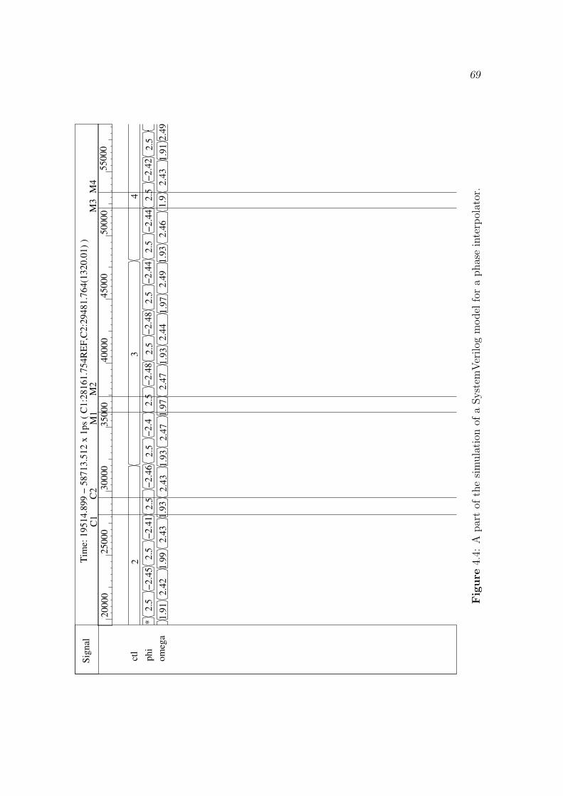
69
M1
40000
35000
30000
25000
20000
*
Tim
e: 1
9514.8
99 −
58713.5
12 x
1ps
( C
1:2
8161.7
54R
EF
,C2:2
9481.7
64(1
320.0
1)
)C
2C
1M
3M
4M
2
2.5
−2.4
52.5
2.5
2.5
2.5
2.5
2.5
2.5
2.5
2.5
1.9
9
2
2.4
21.9
12.4
32.4
72.4
72.4
31.9
31.9
31.9
31.9
71.9
72.4
4
−2.4
8−
2.4
8−
2.4
−2.4
6−
2.4
4−
2.4
2−
2.4
4
2.4
92.4
32.4
62.4
91.9
31.9
−2.4
1
34
1.9
1
55000
50000
Sig
nal
phi
om
ega
ctl
45000
Fig
ure
4.4:
Apar
tof
the
sim
ula
tion
ofa
Syst
emVer
ilog
model
for
aphas
ein
terp
olat
or.
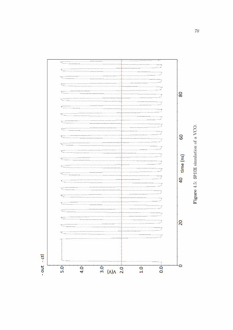
70
Fig
ure
4.5:
SPICE
sim
ula
tion
ofa
VC
O.

71
simulation result in Fig. 4.5 shows the VCO’s transient behavior for the first 12.8 ns
during which it does not oscillate. Since the above component has no control inputs,
the transient and the steady-state behaviors are not differentiated in the model, and
its effect can be seen in the form of wide delay ranges of transitions t1, t4, and t7.
The above problem is solved by redefining the component as c = 〈In = {ctl},
Out = {out}, Care = {ctl, out}, Ctl = {ctl}〉. Fig. 4.7 and Fig. 4.8 show the two
processes of the LPN model that is generated for this component using a tolerance
of 2 percent from the same set of simulation traces. It can be seen in Fig. 4.7 that
each loop in the previous LPN is split into two loops, one when the value of stable
is 0 and the other when the value of stable is 1. The wide delay ranges appear only
in the loop with stable = 0. The LPN process on the left is responsible for assigning
the value of stable.
Though the wide delay range problem does not exist in the above model, it
is still not general enough for being simulated with an arbitrary test-bench. For
example, this LPN works incorrectly if the value of ctl changes any time during the
simulation because such changes are not observed in any of the given simulations. In
other words, after one of the transitions, t18, t19, or t20, fires, the value of ctl is not
allowed to change. This problem can be solved either by inserting pseudo-transitions
or by using the functional approach. The LPN with pseudo-transitions for the
VCO is quite complex, and it proves the fact that pseudo-transitions cause the
complexity of the LPNs to increase exponentially with the size of the model. However,
as mentioned earlier, though the LPN with pseudo-transitions is more complex, it
accurately represents the different behaviors for different sequences of input changes.
The LPN generated using the functional approach is much simpler but it does not
differentiate between the sequences in which the noncare variables change. Fig. 4.9
and Fig. 4.10 show the processes of the LPN that is generated by employing many of
the techniques presented in Chapter 3 (i.e., functional approach, pseudo-transitions,
and transients). In this approach, when the VCO component is defined as c = 〈In =
{ctl}, Out = {out}, Care = {out}, Ctl = {ctl}〉, the LPN process shown in Fig. 4.9
is obtained. This model does not contain any sequence in which the value of ctl
changes in the given simulation traces because ctl is not declared as a care variable.

72
p2 p4p7
p8
p6
[uniform(1.3,1.5)]t5
t0[1.9]
<out:=uniform(4.9,5)>
t3[1.9]
<out:=uniform(4.9,5)>
t6[1.9]
<out:=uniform(4.9,5)>
t7[uniform(1.1,10.7)]
<out:=uniform(0,0.1)>
[uniform(1.5,1.7)]<out:=uniform(4.9,5)>
t9
[0]<out:=uniform(0,0.1)>
t10{¬(ctl ≥ 2.5)}
[0]<out:=uniform(0,0.1)>
t11{(ctl ≥ 3.5)}
[0]<out:=uniform(0.1,0.2)>
p3
p9
t1[uniform(1.3,10.9)]
<out:=uniform(0,0.1)>
t8
p3
<out:=uniform(4.9,5)>
{(ctl ≥ 2.5)&¬(ctl ≥ 3.5)}
t4[uniform(1.1,10.7)]
<out:=uniform(0.1,0.2)>
[uniform(1.7,2)]<out:=uniform(4.9,5)>
t2
p5
p1
Figure 4.6: The LPN model for a VCO without control inputs and don’t cares.
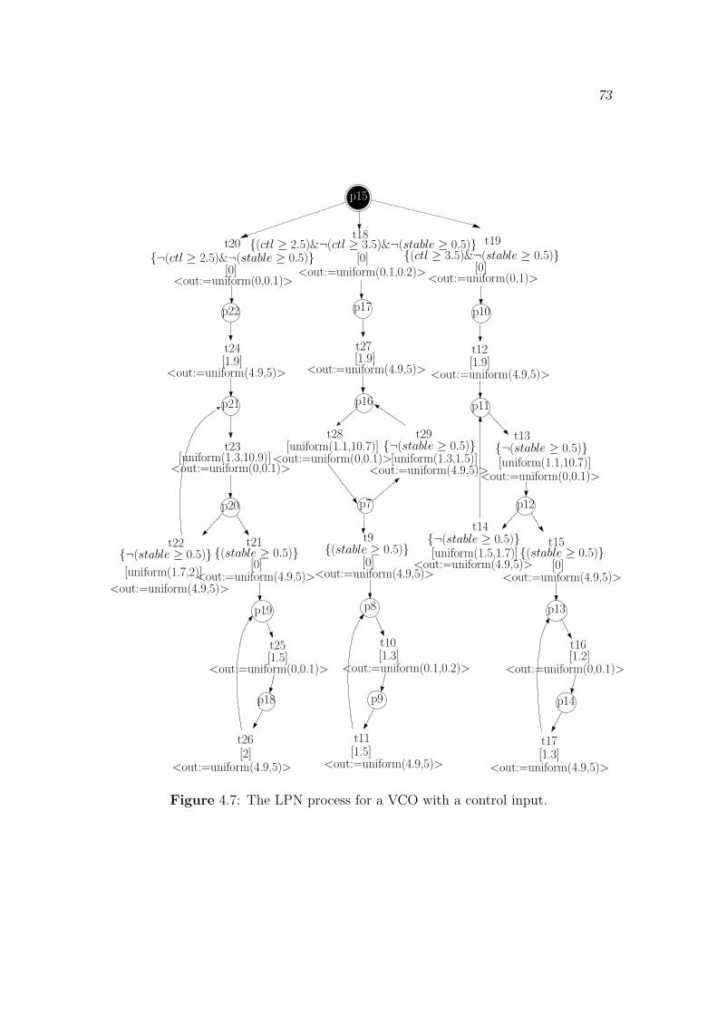
73
p17
p11
p7
[1.2]t16t10
<out:=uniform(4.9,5)>[0]
t15{(stable ≥ 0.5)}
t12[1.9]
<out:=uniform(4.9,5)>
<out:=uniform(4.9,5)>[0]
t9{(stable ≥ 0.5)}
[1.9]t27
{(ctl ≥ 2.5)&¬(ctl ≥ 3.5)&¬(stable ≥ 0.5)}[0]
t18
{(ctl ≥ 3.5)&¬(stable ≥ 0.5)}[0]<out:=uniform(0.1,0.2)>
<out:=uniform(4.9,5)>
{¬(stable ≥ 0.5)}t29
<out:=uniform(0,1)>
t13
<out:=uniform(4.9,5)>[1.5]t11
p8 p13
p14
<out:=uniform(0,0.1)>
<out:=uniform(4.9,5)>
[1.5]t25
{(stable ≥ 0.5)}t21
t23[uniform(1.3,10.9)]
<out:=uniform(4.9,5)>
t24[1.9]
[0]{¬(ctl ≥ 2.5)&¬(stable ≥ 0.5)}
t20
[0]
t22
<out:=uniform(0,0.1)>
t26[2]
<out:=uniform(4.9,5)>
p18
p19
<out:=uniform(0,0.1)><out:=uniform(0.1,0.2)>[1.3]
<out:=uniform(0,0.1)>
<out:=uniform(4.9,5)>
t14{¬(stable ≥ 0.5)}[uniform(1.5,1.7)]
<out:=uniform(4.9,5)>{¬(stable ≥ 0.5)}
<out:=uniform(0,0.1)>[uniform(1.1,10.7)]{¬(stable ≥ 0.5)}
t28[uniform(1.1,10.7)]
<out:=uniform(0,0.1)>
t19
[uniform(1.3,1.5)]
[uniform(1.7,2)]
p9
p16
p20
p21
p15
[1.3]<out:=uniform(4.9,5)>
p22
t17
p10
p12
<out:=uniform(4.9,5)>
Figure 4.7: The LPN process for a VCO with a control input.
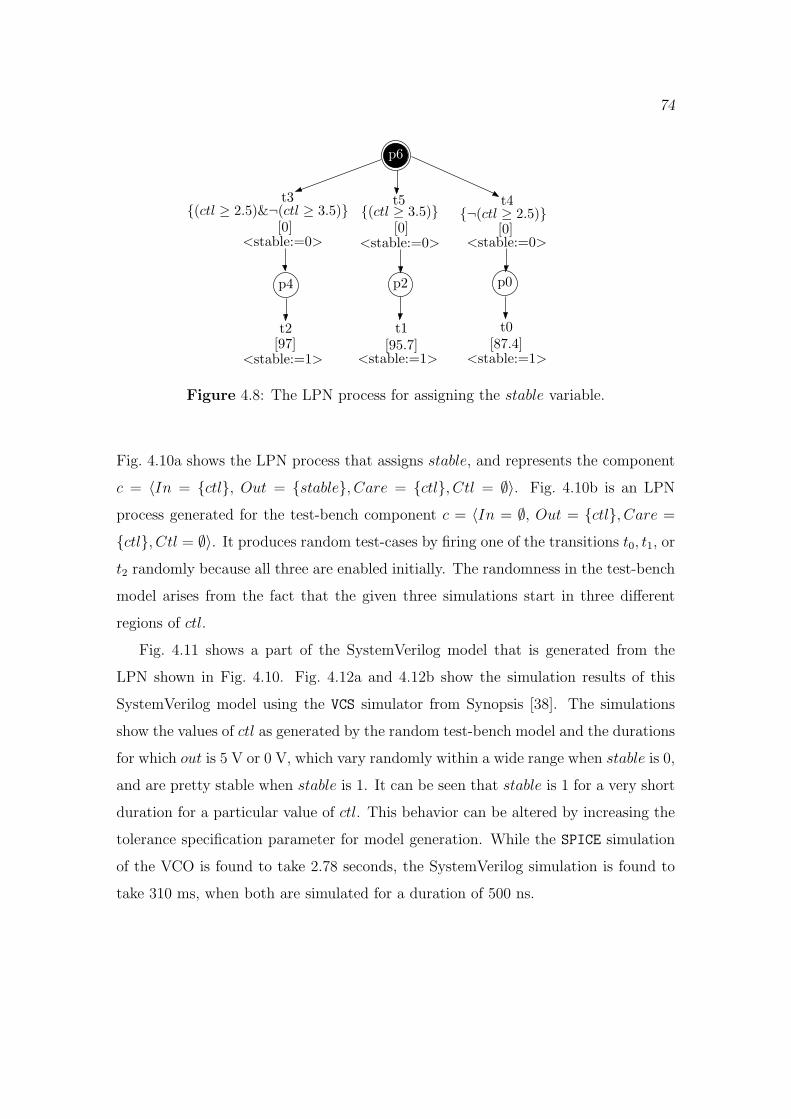
74
t4
p0
[97]<stable:=1>
[95.7]<stable:=1>
[87.4]
<stable:=0>[0]
{(ctl ≥ 2.5)&¬(ctl ≥ 3.5)}t3 t5
{(ctl ≥ 3.5)}
<stable:=0> <stable:=0>[0]
{¬(ctl ≥ 2.5)}
p6
[0]
p4
t2 t0
p2
t1
<stable:=1>
Figure 4.8: The LPN process for assigning the stable variable.
Fig. 4.10a shows the LPN process that assigns stable, and represents the component
c = 〈In = {ctl}, Out = {stable}, Care = {ctl}, Ctl = ∅〉. Fig. 4.10b is an LPN
process generated for the test-bench component c = 〈In = ∅, Out = {ctl}, Care =
{ctl}, Ctl = ∅〉. It produces random test-cases by firing one of the transitions t0, t1, or
t2 randomly because all three are enabled initially. The randomness in the test-bench
model arises from the fact that the given three simulations start in three different
regions of ctl.
Fig. 4.11 shows a part of the SystemVerilog model that is generated from the
LPN shown in Fig. 4.10. Fig. 4.12a and 4.12b show the simulation results of this
SystemVerilog model using the VCS simulator from Synopsis [38]. The simulations
show the values of ctl as generated by the random test-bench model and the durations
for which out is 5 V or 0 V, which vary randomly within a wide range when stable is 0,
and are pretty stable when stable is 1. It can be seen that stable is 1 for a very short
duration for a particular value of ctl. This behavior can be altered by increasing the
tolerance specification parameter for model generation. While the SPICE simulation
of the VCO is found to take 2.78 seconds, the SystemVerilog simulation is found to
take 310 ms, when both are simulated for a duration of 500 ns.

75
p0
<out:=uniform(4.9,5)>[0]
{(stable ≥ 0.5)}t4
p4
[0]
p3
{(stable ≥ 0.5)}
{¬(stable ≥ 0.5)}
pt4
[0]
pt6
p2
(¬(stable ≥ 0.5)&(ctl ≥ 2.5)&¬(ctl ≥ 3.5)) ∗ 1.7)+
p5
[0]
pt7
[0]
{¬(stable ≥ 0.5)}pt5
{(stable ≥ 0.5)}
p1
t1
t3{¬(stable ≥ 0.5)}
(¬(stable ≥ 0.5)&¬(ctl ≥ 2.5)) ∗ 2)+
uniform((¬(stable ≥ 0.5)&(ctl ≥ 3.5)) ∗ 1.3,
<out:=uniform(4.9,5)>
(¬(stable ≥ 0.5)&(ctl ≥ 2.5)&¬(ctl ≥ 3.5)) ∗ 10.7)+
[uniform((¬(stable ≥ 0.5)&¬(ctl ≥ 2.5)) ∗ 1.3,
uniform((¬(stable ≥ 0.5)&(ctl ≥ 2.5)&¬(ctl ≥ 3.5)) ∗ 1.1,
t2
<out:=uniform(0,0.2)>
{¬(stable ≥ 0.5)}
(¬(stable ≥ 0.5)&¬(ctl ≥ 2.5)) ∗ 10.9)+
uniform((¬(stable ≥ 0.5)&(ctl ≥ 3.5)) ∗ 1.1,(¬(stable ≥ 0.5)&(ctl ≥ 3.5)) ∗ 10.7)])
(¬(stable ≥ 0.5)&(ctl ≥ 3.5)) ∗ 1.5)])
uniform((¬(stable ≥ 0.5)&(ctl ≥ 2.5)&¬(ctl ≥ 3.5)) ∗ 1.5,
[uniform((¬(stable ≥ 0.5)&¬(ctl ≥ 2.5)) ∗ 1.7,
((stable ≥ 0.5)&(ctl ≥ 2.5)&¬(ctl ≥ 3.5)) ∗ 1.5+[((stable ≥ 0.5)&¬(ctl ≥ 2.5)) ∗ 2+
((stable ≥ 0.5)&(ctl ≥ 3.5)) ∗ 1.3]
t6
{(stable ≥ 0.5)}t5
[((stable ≥ 0.5)&¬(ctl ≥ 2.5)) ∗ 1.5+((stable ≥ 0.5)&(ctl ≥ 2.5)&¬(ctl ≥ 3.5)) ∗ 1.3+
((stable ≥ 0.5)&(ctl ≥ 3.5)) ∗ 1.2]
<out:=uniform(4.9,5)>[(¬(ctl ≥ 2.5)) ∗ 1.9 + ((ctl ≥ 2.5)&¬(ctl ≥ 3.5)) ∗ 1.9 + (ctl ≥ 3.5) ∗ 1.9]
t0
<out:=uniform(0,0.2)>
{¬(stable ≥ 0.5)}[0]
<out:=uniform(0,0.2)><out:=uniform(4.9,5)>
{(stable ≥ 0.5)}
Figure 4.9: The LPN process for a VCO demonstrating the transients, functionalapproach, and pseudo-transitions.
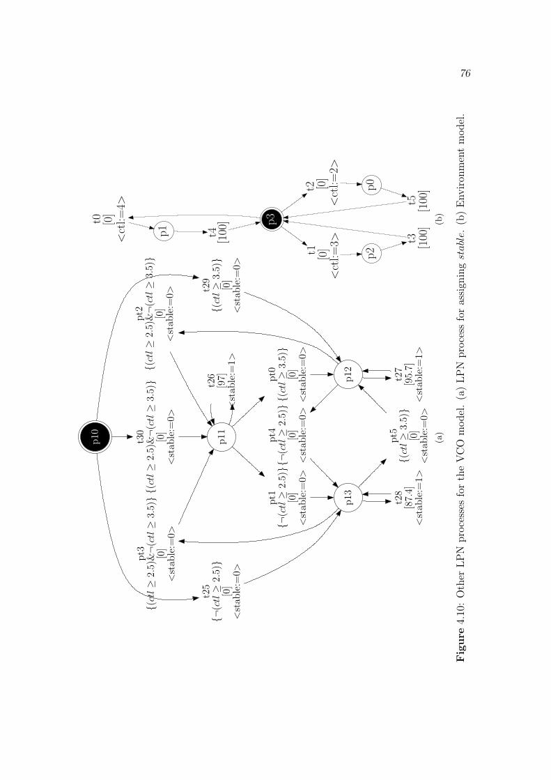
76
[0]
{(ct
l≥
2.5)
&¬
(ctl≥
3.5)}
pt2
{(ct
l≥
2.5)
&¬
(ctl≥
3.5)}
[0]
<st
able
:=0>
[0]
<st
able
:=0>
{(ct
l≥
2.5)
&¬
(ctl≥
3.5)}
p11
t25
{¬(c
tl≥
2.5)}
[0]
<st
able
:=0>
p13
t26
[97]
<st
able
:=1>
t27
[95.
7]<
stab
le:=
1>
p12
t28
[87.
4]<
stab
le:=
1>
t29
{(ct
l≥
3.5)}
[0]
<st
able
:=0>
pt0
{(ct
l≥
3.5)}
[0]
<st
able
:=0>
pt1
{¬(c
tl≥
2.5)}
[0]
<st
able
:=0>
pt4
{¬(c
tl≥
2.5)}
[0]
<st
able
:=0>
pt5
{(ct
l≥
3.5)}
[0]
<st
able
:=0>
p10
pt3
t30
<st
able
:=0>
(a)
[0]
p1
p2
p0
t3
p3
t4
t5
<ct
l:=4>
t1
[100
][1
00]
<ct
l:=2>
[0]
t2
<ct
l:=3>
[0]
[100
]t0 (b)
Fig
ure
4.10
:O
ther
LP
Npro
cess
esfo
rth
eV
CO
model
.(a
)LP
Npro
cess
for
assi
gnin
gsta
ble.
(b)
Envir
onm
ent
model
.
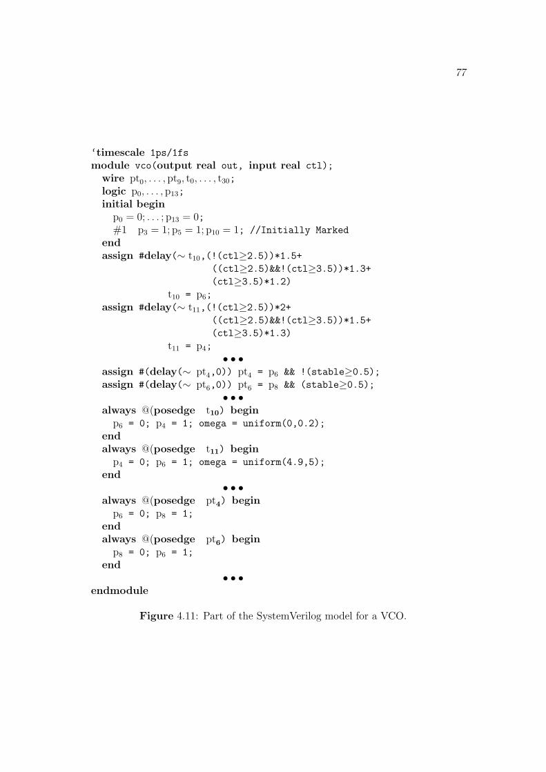
77
‘timescale 1ps/1fs
module vco(output real out, input real ctl);
wire pt0, . . . , pt9, t0, . . . , t30;
logic p0, . . . , p13;
initial beginp0 = 0; . . . ; p13 = 0;#1 p3 = 1; p5 = 1; p10 = 1; //Initially Marked
endassign #delay(∼ t10,(!(ctl≥2.5))*1.5+
((ctl≥2.5)&&!(ctl≥3.5))*1.3+(ctl≥3.5)*1.2)
t10 = p6;
assign #delay(∼ t11,(!(ctl≥2.5))*2+((ctl≥2.5)&&!(ctl≥3.5))*1.5+(ctl≥3.5)*1.3)
t11 = p4;
• • •assign #(delay(∼ pt4,0)) pt4 = p6 && !(stable≥0.5);assign #(delay(∼ pt6,0)) pt6 = p8 && (stable≥0.5);
• • •always @(posedge t10) begin
p6 = 0; p4 = 1; omega = uniform(0,0.2);
endalways @(posedge t11) begin
p4 = 0; p6 = 1; omega = uniform(4.9,5);
end• • •
always @(posedge pt4) begin
p6 = 0; p8 = 1;
endalways @(posedge pt
6) begin
p8 = 0; p6 = 1;
end• • •
endmodule
Figure 4.11: Part of the SystemVerilog model for a VCO.
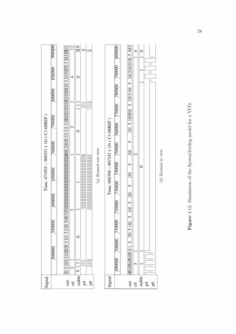
78
Sig
nal
01
23
01
01
24
2
1
55
55
55
55
55
55
55
55
55
55
05
55
5o
ut
ctl
stab
le
p4
p6
Tim
e: 4
71
95
5 −
90
93
51
x 1
fs (
C1
:68
RE
F )
55
55
55
55
50
00
00
55
00
00
60
00
00
65
00
00
70
00
00
75
00
00
80
00
00
85
00
00
90
00
00
00
(a)
Zoom
edout
vie
w
Sig
nal
ou
t
ctl
stab
le
p4
p6
55
55
55
55
55
55
55
55
4 01
00
00
00
00
00
00
00
00
00
00
55
55
3 1
69
00
00
70
00
00
71
00
00
72
00
00
73
00
00
74
00
00
75
00
00
76
00
00
77
00
00
78
00
00
79
00
00
80
00
00
0
2
Tim
e: 6
88
39
8 −
80
72
41
x 1
fs (
C1
:68
RE
F )
(b)
Zoom
edin
vie
w
Fig
ure
4.12
:Sim
ula
tion
ofth
eSyst
emV
erilog
model
for
aV
CO
.
CHAPTER 5
CONCLUSIONS
The complexity of today’s mixed-signal SOCs makes it very difficult to verify
their functionality. Though transistor-level simulations are desired for performance
verification where accuracy is important, functional verification does not need very
accurate circuit models. Though FastSpice is faster than SPICE, using it for func-
tional verification is not very practical because it is utilized too late in the design
cycle when the complete transistor-level design of the system is available, and it
is too slow for simulating the whole system in all the modes of operation [10, 11].
Formal verification tools can prove to be very useful but it is important for them to
be compatible with the current industrial design and verification flows as the analog
designers are reluctant to learn new languages to write formal models for their designs.
The ability to automatically generate abstract models for AMS circuits can prove to
be very useful for performing functional validation.
5.1 Summary
This thesis presents an improved method for automatically extracting behavioral
models from simulation traces. The models generated using the method presented
in [22] have a very limited scope which restricts their ability to replace the actual
circuits as abstract models. A phase interpolator example has been used to illustrate
the problems that exist in this method. The same example is used to demonstrate
the new method’s ability to solve these problems. The three major contributions of
this thesis are :
• A method to represent transient behavior, present in simulation traces, in the
LPN models.

80
• Generalization while extracting the LPN models so that they can be subjected
to arbitrary stimuli for simulation purposes.
• A generic way of representing the extracted LPN models in HDLs like Sys-
temVerilog and automatic translation of LPNs to SystemVerilog accurately.
The improved method is implemented in the LEMA tool and it has been applied
on two industrial examples — a phase interpolator and a VCO. The generated
SystemVerilog models have been verified to function as expected using assertions
and constrained random stimulus generation techniques.
5.2 Future Work
Though the above improvements extend the model generator’s potential, there is
still a significant scope for research in this area. The major research directions in this
area are :
• Linear interpolation of assignments.
• Generation of stable using a functional approach.
• Embedding limitations within the model.
• Guidance for additional simulations.
• Equivalence checking.
• Extension of LPNs to express temporal properties.
• Application to other hybrid system models.
5.2.1 Linear Interpolation of Assignments
The models generated using this model generation method use an approximation
that the behavior within a region is the same. The argument behind this assumption
is that when more simulations in which variables have closer values are used, then
more thresholds are generated and hence the generated model’s accuracy improves.
81
However, approximating the behavior with linear interpolation can be more advanta-
geous than approximating the behavior in the whole region to that at a single point.
Our preliminary investigations show that this can be implemented by constructing
the assignments for the delays, values, and rates on the transitions as expressions by
interpolating between their corresponding values obtained from the simulations.
5.2.2 Generation of stable Using a Functional Approach
The LPN shown in Fig. 4.10 has a stable variable assignment process that is
generated using pseudo-transitions. Ideally, it is desirable to have this process using
the functional approach because of the limitations of pseudo-transitions mentioned
in Section 3.5.3. However, generating this process using a functional approach poses
problems because a change in the values of the control inputs must be detected for
de-asserting stable. Our preliminary investigations revealed that this detection of
a change is possible by storing the previous state of the control inputs in the LPN
model.
5.2.3 Embedding Limitations Within the Model
An important property of the models generated from the simulation traces is that
they do not completely represent the actual circuit and they only represent the circuit
for a limited set of inputs. Thus, it is important that a user knows the limitations
of the generated models. The ability to automatically generate assertions that fire
when a model is subjected to stimuli that do not relate to any of the simulations from
which it is generated adds value to these models.
5.2.4 Guidance for Additional Simulations
Finding the right set of test-cases for a circuit is always a challenging task. Given
the fact that exhaustive simulation is a difficult task, suggesting additional simulations
that exercise corner cases that the designer has not thought of can prove to be a very
useful application of this method. When a model that is generated using a finite
set of simulation traces is used for system-level simulations, it may be subjected
to a stimulus that is not a part of the simulations from which it is generated. If
82
the user is warned in such cases, the model can be regenerated by including such
new test scenarios in the set of simulation traces for model generation. Classifying
the simulations based on their contributions to the model can also be helpful to
the designer. For example, if a model generated from three simulations is proven
to be equivalent to that generated from these three simulations and another extra
simulation, then, providing this feedback to the user can prove to be valuable. The
designer can use this feedback as guidance for new simulations.
5.2.5 Equivalence Checking
Another potential application of this method is in proving the equivalence of two
circuits. For example, a circuit and its optimized version can be simulated for the
interesting test-cases, and the models generated using these simulations can be used to
prove the equivalence between the circuits. If the models generated from the same set
of simulations of both the circuits are the same, then, it implies that the optimization
did not change the circuit’s behavior. A standard equivalence checking method can
also be useful in proving the accuracy of the models generated using this method.
5.2.6 Extension of LPNs to Express Temporal Properties
From the phase interpolator’s property LPN shown in Section 4.1, it can be seen
that expressing even simple properties as LPNs is a tedious task. Representing com-
plex verification properties in the form of LPNs can be a challenging task. Extending
the LPN syntax to allow temporal constructs makes it easy to express complex
verification properties in the LPNs. This ability to express properties using simple
temporal constructs also improves the performance of the SystemVerilog simulations
because each property translates into a single assertion statement. In the current
scenario, each property is constructed as a whole LPN process with a single failure
transition. Thus, a single property translates into a number of assign statements,
procedural statements, and an assertion in SystemVerilog.
83
5.2.7 Application to Other Hybrid System Models
The techniques presented in this thesis are not limited to modeling of AMS circuits,
and have a wider range of applications. In general, they can be used for modeling any
system with continuous and discrete dynamics. One such extension is to generate LPN
models from Simulink models, which are used to perform multidomain simulations of
control and other dynamical systems.

REFERENCES
[1] J. David, “Efficient functional verification for mixed signal IP,” in Proceedingsof the 2004 IEEE International Behavioral Modeling and Simulation Conference,October 2004, pp. 53–58.
[2] IEEE Standard for SystemVerilog – Unified Hardware Design, Specification, andVerification Language (1800-2009), IEEE Computer Society, Dec. 2009.
[3] S. Palnitkar, Design Verification with e. Prentice Hall Professional TechnicalReference, 2003.
[4] E. Barke, D. Grabowski, H. Graeb, L. Hedrich, S. Heinen, R. Popp, S. Steinhorst,and Y. Wang, “Formal approaches to analog circuit verification,” in Design,Automation and Test in Europe. IEEE, April 2009, pp. 724 –729.
[5] M. H. Zaki, S. Tahar, and G. Bois, “Formal verification of analog and mixedsignal designs: A survey,” Microelectronics Journal, vol. 39, no. 12, pp. 1395 –1404, 2008.
[6] B. I. Silva and B. H. Krogh, “Formal verification of hybrid systems usingCheckMate: A case study,” in Proc. American Control Conference, vol. 3. IEEEPress, Jun. 2000, pp. 1679–1683.
[7] G. Frehse, “PHAVer: Algorithmic verification of hybrid systems past HyTech,”in International Workshop on Hybrid Systems: Computation and Control, ser.Lecture Notes in Computer Science, M. Morari and L. Thiele, Eds., vol. 3414.Springer-Verlag, 2005, pp. 258–273.
[8] E. Asarin, T. Dang, and O. Maler, “The d/dt tool for verification of hybrid sys-tems,” in Proceedings International Workshop on Computer Aided Verification,ser. Lecture Notes in Computer Science, E. Brinksma and K. G. Larsen, Eds.,vol. 2404. Springer-Verlag, 2002, pp. 365–370.
[9] S. R. Little, D. Walter, and C. J. Myers, “Analog/mixed-signal circuit verificationusing models generated from simulation traces,” in Automated Technology forVerification and Analysis (ATVA), ser. Lecture Notes in Computer Science, K. S.Namjoshi, T. Yoneda, T. Higashino, and Y. Okamura, Eds., vol. 4762. Springer-Verlag, 2007, pp. 114–128.
[10] Cadence, Virtuoso UltraSim Full-Chip Simulator Datasheet, 2010.
[11] Synopsys, CustomSim Unified Circuit Simulation Solution For Nanometer De-signs, 2009.
[12] Cadence, Virtuoso SpectreRF Simulation Option User Guide, 5th ed., 2005.

85
[13] S. Joeres and S. Heinen, “Functional verification of radio frequency SoCs usingmixed-mode and mixed-domain simulations,” in Behavioral Modeling and Sim-ulation Workshop, Proceedings of the 2006 IEEE International, Sept. 2006, pp.144 –149.
[14] T. Dang and T. Nahhal, “Coverage-guided test generation for continuous andhybrid systems,” Formal Methods in System Design, vol. 34, pp. 183–213, April2009.
[15] S. Steinhorst and L. Hedrich, “A formal approach to complete state space-covering input stimuli generation for verification of analog systems,” in Ana-log 2008: 10. ITG/GMM-Fachtagung Entwicklung von Analogschaltungen mitCAE-Methoden, 2008.
[16] B. C. Lim, J. Kim, and M. A. Horowitz, “An efficient test vector generationfor checking analog/mixed-signal functional models,” in Design AutomationConference. New York, NY, USA: ACM, 2010, pp. 767–772.
[17] S. Ray and J. Bhadra, “A mechanized refinement framework for analysis ofcustom memories,” in Proceedings of the Formal Methods in Computer AidedDesign. Washington, DC, USA: IEEE Computer Society, 2007, pp. 239–242.
[18] A. Antoulas, D. Sorensen, and S. Gugercin, “A survey of model reductionmethods for large-scale systems,” Contemporary Mathematics, vol. 280, pp.193–219, 2001.
[19] S. Gugercin and A. C. Antoulas, “A survey of model reduction by balancedtruncation and some new results,” International Journal of Control, vol. 77,no. 8, pp. 748–766, 2004.
[20] M. Rewienski and J. White, “A trajectory piecewise-linear approach to modelorder reduction and fast simulation of nonlinear circuits and micromachineddevices,” IEEE Transactions on Computer-Aided Design of Integrated Circuitsand Systems, vol. 22, no. 2, pp. 155–170, Feb. 2003.
[21] N. Dong and J. Roychowdhury, “Piecewise polynomial nonlinear model reduc-tion,” in Design Automation Conference. New York, NY, USA: Association forComputing Machinery, 2003, pp. 484–489.
[22] S. R. Little, “Efficient modeling and verification of analog/mixed-signal circuitsusing labeled hybrid Petri nets,” Ph.D. dissertation, University of Utah, Dec.2008.
[23] G. E. Fainekos, A. Girard, and G. J. Pappas, “Temporal logic verification usingsimulation,” in Formal Modelling and Analysis of Timed Systems (FORMATS),ser. Lecture Notes in Computer Science, E. Asarin and P. Bouyer, Eds., vol.4202. Springer-Verlag, 2006, pp. 171–186.
[24] D. Nickovic and O. Maler, “AMT: A property-based monitoring tool for analogsystems,” in Formal Modelling and Analysis of Timed Systems (FORMATS),2007.
86
[25] D. Nickovic, “Checking timed and hybrid properties: Theory and applications,”Ph.D. dissertation, University Joseph Fourier, 2008.
[26] T. R. Dastidar and P. P. Chakrabarti, “A verification system for transientresponse of analog circuits,” ACM Trans. Des. Autom. Electron. Syst., vol. 12,no. 3, pp. 1–39, 2007.
[27] E. M. Clarke, O. Grumberg, and D. A. Peled, Model Checking. The MIT Press,1999.
[28] S. Sidiropoulos and M. Horowitz, “A semidigital dual delay-locked loop,” IEEEJournal of Solid-State Circuits, vol. 32, no. 11, pp. 1683 –1692, Nov. 1997.
[29] R. Alur, T. A. Henzinger, and P. Ho, “Automatic symbolic verification ofembedded systems,” IEEE Transactions on Software Engineering, vol. 22, no. 3,pp. 181–201, 1996.
[30] R. Alur, T. Dang, J. Esposito, Y. Hur, F. Ivancic, V. Kumar, P. Mishra, G. J.Pappas, and O. Sokolsky, “Hierarchical modeling and analysis of embeddedsystems,” Proc. of the IEEE, vol. 91, no. 1, pp. 11 – 28, January 2003.
[31] F. Balduzzi, A. Giua, and G. Menga, “First-order hybrid petri nets: A modelfor optimization and control,” IEEE Transactions on Robotics and Automation,vol. 16, no. 4, pp. 382–399, 2000.
[32] R. David and H. Alla, “On hybrid Petri nets,” in Discrete Event DynamicSystems: Theory and Applications, vol. 11. Kluwer Academic Publishers, 2001,pp. 9–40.
[33] D. C. Walter, “Verification of analog and mixed-signal circuits using symbolicmethods,” Ph.D. dissertation, University of Utah, Aug. 2007.
[34] S. R. Little, N. Seegmiller, D. Walter, C. J. Myers, and T. Yoneda, “Verificationof analog/mixed-signal circuits using labeled hybrid Petri nets,” Computer-AidedDesign, International Conference on, vol. 0, pp. 275–282, 2006.
[35] R. Thacker, “A new verification method for embedded systems,” Ph.D. disser-tation, University of Utah, Dec. 2009.
[36] K. S. Kundert and O. Zinke, The Designer’s Guide to Verilog-AMS. Springer,June 2004.
[37] S. R. Little, D. C. Walter, C. J. Myers, R. Thacker, S. Batchu, and T. Yoneda,“Verification of analog/mixed-signal circuits using labeled hybrid Petri nets,”IEEE Transactions on Computer-Aided Design of Integrated Circuits and Sys-tems, 2006.
[38] Synopsys, VCSTM/VCSiTMUser Guide, 2004.