automatic inspection for printed wiring - robotics · pdf filesuch viewing the effective...
TRANSCRIPT

Automatic inspection for Printed Wiring
Hobcrt 'I'hibadcau, Mark Fricdriian and John Scto'
CM U-KI-'i'R-82-16
The Robotics Institute Carncgie-Mcllon Univeriity
Pittsburgh, Pennsylvcinia 15213
Copyright @ 1983 Carnegie-Mellon University
Papcr prcsentcd at The Institutc for Interconnecting and Package Electronic Circuits, Fail Mccting, San Dicgo, CA, Octobcr 3, 1982.
'Wcstinghouxc Dcfciisc and Electronic Systcms


Table of Contents 1. Introduction 2. Guidelines for an Inspection Station 3. Types of Inspection Stations 4. How Design Rule Systems Work, and Don’t Work 5. What happened to Truly Automatic Inspection Stations? 6. Flexible if not Ideal Stations 7. Conclusions
1 3 7 9 10 12 13


Abstract
Cooperation bctwccn t!ic Robotics Institutc mil Wcstingliousc Cciporatior. has resulted i n the
devclopmcnt uf guidclincs, or spccifications. for a PlYU inspcction station. ‘Ihcsc guidelines ar‘c presented in
this technical rcport. Although PM’n iiispcction ststions primarily servc quality control funciions, they hold
grcat potcntial in scrving functions of process control. I>iscussed in this rcport is what can reaqonably be
expected from state-of-thc-art PlVB inspcction aids, tjjpes of stations and how they work.


1
1 . Introduction Twenty years ago academic literature on computer vision contained many computer analyses of
images of printed circuit boards. Even the most recent textbooks on image processing will illustrate
several algorithms on pictures of printed circuits. The algorithm shows how to detect a defect in a
printed circuit from the visual image of it. Every time, (of course), the algorithm succeeds in defecting
the defect. But for all these twenty years, and all those examples of defect detection, there has yet to
be a successful commercial product for the visual inspection of printed circuits by machine. Perhaps
the printed circuit industry lacked incentive for automated visual inspection. But now there is a need,
and researchers are learning that automated printed circuit board inspection is a hard problem to
solve.
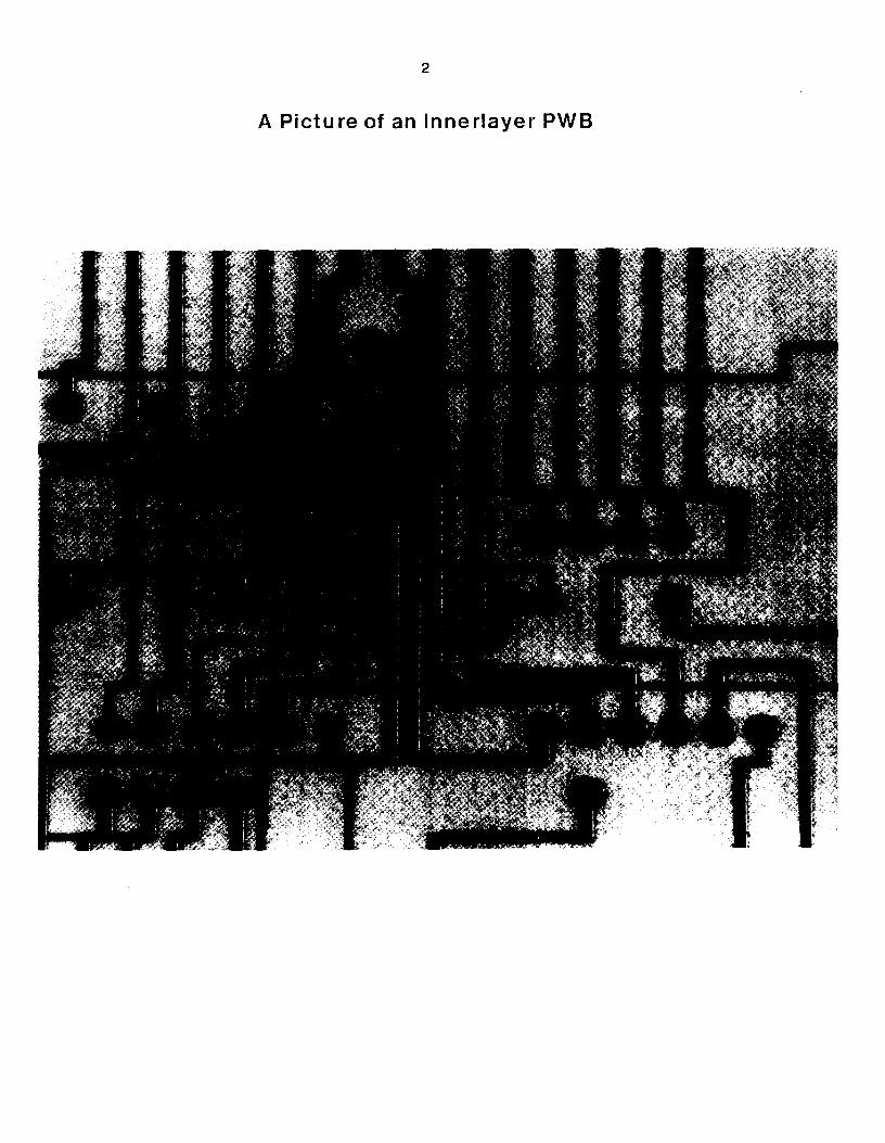
Figure 1 provides an example of a printed circuit - - in this case an image taken at low magnification
to give the idea of the patterns on a printed circuit board. The pattern is in copper, and the reader may
note the image from the copper on the other side of the board. Modern printed circuit boards (PCBs),
or printed wiring boards, (PWBs) use wiring of finer design, greater density, and more printed layers
to a single board. The image in Figure 1 is a layer of a twelve-layer board. Already more than 15% of
the labor force is likely to be involved in visually inspecting such layers. As line widths go from twenty
mils to two mils, the cost of inspection is greatly affected. A major reason is that the tenfold decrease
in line widths and spacing requirements is really a hundredfold increase in inspection area.
Furthermore, there is greater need to see the board under magnification. For twenty mil boards, a 3X
magnifying glass is enough, but, for two mil boards, there is a need for 30X microscopic viewing. With
such viewing the effective inspection area is ten thousand times larger.
This scaling effect is only a part of the problem. Finer line technologies promote more dependence
on single boards. A single board becomes more valuable because more circuitry and components
can be put on it, and this means the cost of missing a defect increases. Finally, current technology
promotes the use of multilayer laminated boards. A 10% probability of a defect in a single layer
translates to better than a 60% probability of a defect in a 10 layer laminate [5]. The effects of such a
Bernouli probability process are quite scary, and (manufacturers are discovering) the fears are not at
all relieved by current actualities.
Two years ago there were a few good research and development projects underway for inspection
stations; now we count the projects in the tens. More than one large company is promising, .or
2
A Picture of an Innerlayer PWB

3
strongly hinting at, commercially available inspection systems in the next months.' The prototype
pictured in Figure 2 was just recently completed in the Inspection Laboratory of the Robotics Institute.
Since only a few prototypes have yet been built, and since such promises of production quality
machines have been made before without result, there is reason to stand back from our claims. But
there is a consensus among those who have looked at the problem in depth that robust inspection
systems will be commercially available within a year.
The time has come to provide the PWB industry with what can reasonably be expected from state-
of-the-art PWB Inspection. The devices are inspection aids. They will not carry out autonomous
inspection, as once hoped, but they will flag certain restricted problems with printed wiring boards,
and a human operator cum inspector will still have to make the final decisions. The economic
incentive for such stations stems from the fact that they succeed in aiding the human inspection task.
This is largely because they will act to direct human attention to just those parts of the PWBs that are
suspicious. We will not have to look in great detail at every part of the board. Machines will do much
of the looking.
2. Guidelines for an Inspection Station A valuable result of the cooperation between the Robotics !nstitute and Westinghouse Corporation
has been the development of a set of guidelines or specifications for a PWB inspection station. Table
1 provides a synopsis which has been altered slightly to be sensitive to industry standards rather than
the needs specific to Westinghouse Defense and Electronic Systems and the Robotics Institute
Inspection Laboratory. There have been several collaborations between corporate users and
research and development groups which have resulted in the development of such guidelines. In our
experience, the guidelines developed elsewhere have been similar. The guidelines are broken down
into four categories, relevant to the end user. The Layer Characteristics represent a
generalization of current PWB layer characteristics across a large number of companies. We
assume, for example, that boards will not generally exceed 18 inches in width and that copper or
copper treated patterns predominate. In one respect, namely, the conductor or line width and
spacing, we try to anticipate additive technology boards. It is likely that line widths below four mils (by
spec) will be additive technology boards as opposed to the subtractively etched boards more
common nowadays.
'We witnessed Hughes Corporation announce their "System 9126" automated inspection system at the IPC Conference, and we know that ltek Corporation, Automation Engineering Corporation, and Elron Ltd., are accepting orders of one form or another for 'off the shelf' technology.

4
The CMU PWB Inspection Station

5
Table 1 . PWB Design Rule inspection Station Guideline
I. Layer Characteristics
a. 18"x24" panels (upwards of 300 sq. in. of inspection area per side)
13. Multiple images on a panel
c. Copper or (oxide) treated copper patterns
d. Substrate thickness > = 0.003" (epoxy glass, polyimide, teflon-based
laminates)
e. Conductor patterns/groundplane/powerplane/solid copper
f. Conductor width/spacing > = 0.002"
g. Registration Techniques generally adaptable to pinning for registration
h. Subtractive or additive copper patterns
II. Defect Detection Requirements
a. Open conductor
b. Shorted conductor
c. Spacing below minimum
d. Conductor width below minimum
e. Locally reduced conductor width
1. nicks
2. pinholes
f. Spurious copper
g. Special Types: Measling, Additive Technique Gapping, eta.
I l l . Performance Requirements
a. Process both sides to keep up with Scheduling and
Cost Requirements
1. Online Inspection ( < 2 Minutes)
2. OffLine Inspection (< 15 Minutes)
b. < = 0.5% Escape Rate (number of defect escapes/total number of
actual defects)
c. < = 5% False Alarm Rate (number of false alarms / [number of false
alarms + number of total defects detected])
d. Identify types of defects and location

6
Table 1 continued.
IV. Inspection Station Features
a. Provide Performance Data in Machine Compatible Form
1. type of defect and quantity
2. part number
3. job number
4. disposition
b. Record location of defect on the innerlayer with ink
d. 98% availability (operational time/(operational time + down time))
f. Manual and Computer access of design data
i. Provision for meaningful operator interaction
j. Automatic load and/or unload capability (generally not yet available)

7
The Defect Detection Requirements focus on the two most significant classes of defects, opens
and shorts, and on military specification (generally tighter than commercial specification). We would
like to regard ll.g., special defects, as a catch-all class of defect patterns not of immediate concern
to inspection aids. True inspection devices must detect even that improbable human hair that
appears in the substrate causing a short between conductors.
The Performance Requirements were selected because we believe that current technology
provides at least this level of system performance. A caution is in the area of identifying the types of
defects. The "types" of defects current stations are likely to identify may be somewhat different from
the "types" of defects cited in quality control manuals.
The Inspection Station Features have to do with man-machine interaction, and are generally
meant to provide a baseline criterion for performance. A number of assumptions have been made
which may not be pertinent to a given application. The general aim in these features has been to
point up a very important capability for PWB inspection stations. This is to provide information to
affect quality control, process control, and process capability studies. A significant benefit of
automated, viz., computer based, PWB inspection stations is that they can be made to provide
information about the inspections without additional human involvement. We will return to this point
later.
3. Types of Inspection Stations Generally, there are two classes of inspection stations: the comparator station and the design rule
station. Both have their place. The comparator station can look at a PWB with knowledge about the
proper location and orientation of every feature of the board. It does a one-to-one comparison of the
features of a known 'good' board to the board in question. A recently published description of such a
station is by Hara, Akiyama and Karasaki [2].
The design rule station requires considerably less information and less precision and is, therefore,
more economic. It detects whether a board in question contains features which violate design rule
specifications. Such specifications are similar to those found in quality control documents - - for
example, a line must end in a pad. The stations currently on the market are all design rule systems.
Relevant research publications include work done by Ejiri, Uno, Michihiro, and lkeda [l], Jarvis [3], and Sterling [4].
A comparator station is more powerful in principle, since it also detects whether general design
rules are met by virtue of the fact that these are an attribute of the specific design. Comparisons of an
a
artwork master against the CAD database for the printed circuit will detect whether a line was left out
or misplaced. Comparisons of a printed circuit board against master or CAD database entry will
determine whether the manufactured printed circuit board mirrors the master copy. A final type of
corriparison capitalizes on the fact that in some settings, a single board may contain two ostensibly
identical prints, side by side, later to be routed out as separate PWEs. These ostensibly identical
prints can be compared.
Comparator systems fail when defects are hidden by imprecision in aligning or correlating the test
board against the known good board. Unfortunately, alignment is extremely difficult for printed
wiring. More often than not, to get a comparator system to detect defects, one must also accept a
very high false alarm rate. Comparator systems are designed to flag everything which is different than
the master. However, the sensitivity is often too high because of uncontrolled conditions and this
results in false alarms. Too many false alarms and you might'as well put a human inspector back on
the task.
Design rule systems are advantageous when there is a question of monetary cost and inspecting
artwork masters is less an issue. These systems guarantee that certain abstract features of the
boards agree with specifications. Rarely is there as much need in such systems for the precise
registration of boards. Access to a design database is less critical in the use of such stations. Most
admirably, such stations are less likely to give high false alarm rates.
In their crude forms, neither type of system has the capability of differentiating among different
types of defects or of differentiating severe from less severe defects. But, in practical fact, they permit
some primitive level of defect classification. Comparator systems that do raw comparisons are the
worst in this regard. About the most we can expect from them is whether something was 'extra' on
the board or 'missing' - - not even what that something is. Current comparator schemes work because
the comparison is not done between images, per se, but between abstract features derived from
images.
The work at The Robotics Institute has focused on design-rule systems for a number of reasons. A
major reason is that workable comparator systems tend to borrow from design-rule technology.
Gleaning abstract features from an image is the basic work to be done in a design rule system.
Another reason is that rapid defect detection will inevitably have a heuristic component. That is to
say, there will be some defects that will be missed and some patterns that will be identified as defects
but for the wrong reasons. No method, or combination of methods, we have encountered detects all
the copper defects which can occur on printed wiring boards.

9
Current technology suggests that design rule systems are what you can buy today. Tomorrow,
expect comparator systems which borrow on the methods developed in the design rule research and
development.
4. How Design Rule Systems Work, and Don't Work It is important to understand that design rule systems do not faithfully reproduce the will of their
creators. The technology is such that the limitations enforced by experience, time, and cost affect the
performance of the system. Typically, a design rule system is built around a single method, or
algorithm, which has a characteristic response to a restricted number or class of spatial patterns.
Defects are often non-predictable in shape and severity. The machine may look for defects or for
deviations from the spatial patterns which are deemed "good". A given algorithm may work well in
finding breaks in the conductors, but may fail miserably in finding shorts between pads and
conductors. An overview of a number of algorithms and their characteristic responses can be found
in Thibadeau [5].
There appear to be two classes of design rule algorithms in current machines. The first is
associated with a "software" approach and the second with a "hardware" approach. It is unclear
whether the functionality of the machines can be distinguished by a hardware or software approach,
and the problems of getting software to work rapidly enough are largely surmountable nowadays.
The user may never know whether he has a "software" or a "hardware" machine. Nevertheless, the
principles of operation tend to be quite different and are worth noting.
A hardware machine will typically take several "masks"2 in rapid succession and apply the masks,
left-to-right, top-to-bottom, across every part of the image of the circuit. If a mask at some point
matches the image to some criterion or in some logical way, the mask is deemed to account for the
pattern.lf a copper pattern is present but no mask matches it, or a mask sensitive to a type of defect
matches, then the system registers a defect. For example, consider a mask made up of concentric
circles. The mask detects pinholes when the center circle is filled with substrate (or background), but
the outer one is filled with copper (or foreground). Masks can be worked out to detect legitimate
geometries and types of defects in this fashion. Unfortunately, this approach often yields a strange
categorization of defects. Several masks may detect a defect, each implying a different
manisfestation,
*The term "masks" is just one of many that have been used: We might just have well used a mathmatical Sense of "operator" or "window" as we did in our oral presentation. The most precise term is "operator".

10
A "software" machine does not work rapidly enough to apply the mask approach. Such a machine
will typically work to characterize areas of copper on the basis of some computationally simple
criterion or set of criterions. For example, the software machine may formulate regions of copper and
ask questions about the local horizontal width of a region. If the width is too small and the context
indicates the region is a vertical line, then the inference is that the line is too thin. A round pad will
cause problems since it too may contain a line across it which is very short (at the top and bottom for
horizontal lines drawn across the pad). Such software systems use ingenious ways to avoid false
alarming like this on legitimate geometries.
A problem for any inspection approach is what we will call the "put and punch" method of PWB
fabrication. One puts on a pattern and then punches out some parts of it by drilling. A difficult
problem in present technology is to inspect boards with drilled-through pads in which one allows a
certain degree of "break-out" - - the drill hole creates a half-moon of the pad. The reason this is
difficult is that the drill hole upsets the geometry of the pattern unpredictable ways. If we require that
the drill hole leave a ring of copper around it, then many detectors will work. But the difference
between a sharp edge of copper caused from a drill hole misaligned on a pad, and a sharp edge of
copper caused by overetch is very difficult for such systems to "see". We do not expect this difficulty
to remain forever, but, the reader may note, even comparator systems will have to deal with "put and
punch" playing havoc with otherwise orderly geometries.
A major point of this section has been to emphasize that the manner in which the inspection station
views the circuitry is quite different from the manner in which we, as humans, view it. The method is
typically quite simple, although ingenious. It does not guarantee defect detection unless the defects
meet certain specifications themselves. We all know that defects are not planned, and therefore
some will remain elusive.
5. What happened to Truly Automatic Inspection Stations? Ten years ago, which is at least ten years after academics began talking in earnest about the
problem, automated PWB inspection was a common thought in the PWB industry. That idea, though,
was an ambitious one. The inspection was to be a real inspection by computer. The computer would
look down on the printed wiring board and decide what was going right or wrong with the
manufacture. Defects would be routinely trapped, fabrication processes automatically tuned, and a
description of defects and actions taken sent to management personnel. No one would question
whether the dauntless machine would miss a defect. No one would worry that the machine would cry
wolf one too many times. The only questions that might arise would be questions of bad

11
programming or defective hardware.
Needless to say, a long time has passed. We believe much of the problem lay in the fact that in both
academics and industry the problem has been severely underrated. PWB inspection is a hard
problem. Furthermore, it is not all simply a problem of taking a technology and applying it. It is not a
hard problem simply because one engineer may disagree with another about a defect. There are
fundamental research issues which require satisfactory resolution before the dream of real automated
PWB inspection stations will come to pass.
The most fundamental of those research issues concerns defect understanding. When an engineer
looks at printed wiring and sees something is amiss, he will carefully size up the problem. He is
interested in saving the board, evaluating the performance of the fabrication process, and, over time,
evaluating process capability and the potential for better productivity in his plant. An experienced
engineer, the person we would like the automated inspection station to emulate, sizes up the problem
very quickly. Most of the time he simply looks and knows what is happening. He is doing something
that humans do very well. This form of visual recognition requires finding the defining visual
attributes of an object. The objects in our case are "a short", a "line break", a "case of overetch", a
"speck of dust on the artwork master", and so forth. Despite the many quality control documents
explaining these 'objects' to people, it is far more difficult to explain these 'objects' to computers.
The defining attributes are, to put it bluntly, a total mystery.
The traditional example of this problem is recognizing a dog. Few of us have difficulty seeing a dog
as a dog. But what is it about the vision of the dog that makes i t clear that the thing is a dog and not a
cat or a wolf, for example? Dogs take on a veritable infinity of shapes and sizes, yet we have no
difficulty seeing them for what they are. To date, we still do not have good ways of having machines
do this primitive kind of visual recognition. We hold that it is precisely this kind of recognition that the
engineer uses, and it is precisely this kind of recognition that an automated PWB station will require to
perform well.
In contrast to other technologies where a problem was underrated, we believe that PWB inspection
technology can address this very fundamental question quite directly. The first machines will do
economically viable jobs of detecting most defects most of the time. Defect categories, like line
breaks and shorts will be distinguished, but the distinctions may not always agree with common
sense. They will reflect hard, and most often oversimplified, definitions programriied into the
automated inspection aid. Nevertheless, these machines will provide the economic incentive to build
better machines. As long as circuit patterns remain reasonably constant (aside from any changes in

12
scale), the development of PWB inspection methods can build on experience. With attention to the
problem, something very close to an ideal PWB Inspection Station will be a technical and economic
possibility.
6. Flexible if not Ideal Stations As market forces come into play, PWB inspection stations are likely to become spare and rather
stripped down beasts of burden. But there are hidden costs to computer technology (and fairly well
hidden advantages) which deserve open discussion before we strip the beast of all its purported
luxuries. A major issue is in how to exercise the process control capability of PWB inspection
stations. We do not want another information engine on the factory floor which spits out enormous
quantities of detailed information. We would rather have decisions that the process and quality
control engineers would make, supposing they had the time and resources to study all that
information. This high-level information is better if the system can also explain the decisions.
The inspection device developed at the Robotics Institute is constrained to provide for two stage
processing [5]. The first fast-flagging, or coarse analysis, stage implements a state-of-the-art
inspection aid, as has been described above. Using the "software" approach, defects are flagged for
attention by the station operator. The operator can then examine the board at specific locations to
determine the disposition of the board. The inspection devices currently available, and likely to be
available in the next couple of years, are going to require at least this level of operator intervention.
However, we also provide a second machine processing stage which is distinguished by cropping
the image of the defective area and submitting that image to more intensive, finer image processing.
This processing can exhaustively measure line widths and pad features and can also proceed to
classify the defect patterns in a more motivated way than is available with simple ingenious
algorithms. In our view, the fast-flagging stage can be implemented as either a "hardware" or a
"software" inspection aid, but, in either case, it is appropriate to make provision for a "software"
second stage, or follow-up analysis by the machine. This second stage should not simply have
available the result of the first stage - - it should also have available the information, the image, which
was examined by the first stage. It is important to emphasize that this second stage is not meant to
'make up for the sins of the first'. If the first stage fails to detect a defect, the second stage will not
have the opportunity to see the defect. The purpose of the second stage is to provide a logical
interface between the way the machine coarsely scans a board and the engineer's need to
understand the 'experience' of the machine.
A natural question is why not do this second stage analysis while one is doing the first stage

13
analysis. The second stage analysis takes enough time that it is unreasonable, even with special
purpose hardware, to apply that analysis to every square inch of the PWB. Consider the size of the
image that the machine is dealing with. For boards with ten mil line widths, one is likely to use a
system in which the smallest picture element, or pixel, is 2/3 of a mil square (the considerations on
pixel size have to do with the capacity to measure minimum line width violations). Four hundred
square inches of inspection surface means that approximately a billion picture elements will require
inspection in, say, 100 seconds. The data-rate for this specification is 10 million picture elements a
second. This is a sizable data-rate by present standards. We cannot expect an inspection system to
do much more than flag potential defects at this data-rate.
The flexibility of inspection is improved with two stages. The flexibility is in defining defect
categories and in adjusting the level of report to the end user. It is clear that PWB manufacturing
plants have different ideas about defect patterns. A good example is "spurious copper". One group
may consider "spurious copper" to be any copper that is found on a board out of place, while another
group may consider "spurious copper" to be copper which is out of place but only in a position to
cause a short when the board is drilled (copper causing a directly observable short is typically just
called a "short"). Inspection aids will flag the spurious copper, but it is more economic to catch the
difference between definitions in the second stage analysis.
The end user wants the inspection station to provide not only the service of inspection but a
measurement of conductor and spacing dimensions as well. Do not expect current technology
devices to be 'measuring' in the same way a quality control document stipulates. Current devices
may check whether a line width is within a range, but may never actually compute the average
number of mils for that line width. The second stage analysis is a natural place for such
measurement. Furthermore, it is natural to permit some adjustment or selection among second stage
tasks. I f an engineering decision is made to do a process capability study, perhaps on a new etching
method, the engineer can set the inspection device to do a more careful analysis. This extra analysis
costs time. Perhaps more time than is acceptable on a routine inspection. The value of the device is
the combination: its capability to do fast, routine, work, and more time consuming process control
studies.
7 . Conclusions Automatic visual inspection of PWBs is a technology which is just about to arrive. A new machine
will appear on the factory floor which actually looks at what it is doing. The arrival of this machine has
been marked by years of research, and it is likely that years more of research will be invested in its

14
perfection. But for now, a practical and economically rewarding device is available. As in any new
technology, it is important to consider the long-term goals as well as the short-term rewards. PWB
inspection stations primarily serve quality control functions, but hold great potential in serving
process control functions. We are on the verge of having devices which can bring tireless and
intelligent vision to the process of PWB fabrication.

15
References
[l] Ejiri, M., Uno, T., Michihiro, M., and Ikeda, S. A process for detecting defects in complicated patterns. Computer Graphics and Image Processing :326-339, 1973.
Hara, Y., Akiyama, N., and Karasaki, K. Automatic inspection system for printed circuit boards. Conference Record for 1982 Workshop on Industrial Applications of machine vision, May 3-5.
[2]
162-70, 1982.
[3] Jarvis, J.F. A method for automating the visual inspection of printed wiring boards. IEEE Transactions on pattern analysis and machine intelligence , January, 1980.
[4] Sterling, W. Nonreference optical inspection of complex and repetitive patterns. In J.J. Pearson (editor), Techniques and Applications of Image Understanding, pages 182- 1 BO.
SPIE, April 21 -23, 1981.
[5] Thibadeau, R. Printed Circuit Board Inspection. CMU-RI-TR-81-8, The Robotics Institute, 1981.