automotive power datasheet tle7184f-3v
TRANSCRIPT

Automot ive Power
Datasheet Rev.1.2, 2016-01-27
TLE7184F-3VSystem IC for B6 motor drives

TLE7184F-3V
Table of Contents
Table of Contents
Table of Contents . . . . . . . . . . . . . . . . . . . . . . . . . . . . . . . . . . . . . . . . . . . . . . . . . . . . . . . . . . . . . . . . 2
1 Overview . . . . . . . . . . . . . . . . . . . . . . . . . . . . . . . . . . . . . . . . . . . . . . . . . . . . . . . . . . . . . . . . . . . . . . . 4
2 Block Diagram . . . . . . . . . . . . . . . . . . . . . . . . . . . . . . . . . . . . . . . . . . . . . . . . . . . . . . . . . . . . . . . . . . . 5
3 Pin Configuration . . . . . . . . . . . . . . . . . . . . . . . . . . . . . . . . . . . . . . . . . . . . . . . . . . . . . . . . . . . . . . . . 63.1 Pin Assignment TLE7184F-3V . . . . . . . . . . . . . . . . . . . . . . . . . . . . . . . . . . . . . . . . . . . . . . . . . . . . . . . 63.2 Pin Definitions and Functions . . . . . . . . . . . . . . . . . . . . . . . . . . . . . . . . . . . . . . . . . . . . . . . . . . . . . . . . 7
4 General Product Characteristics . . . . . . . . . . . . . . . . . . . . . . . . . . . . . . . . . . . . . . . . . . . . . . . . . . . . 94.1 Absolute Maximum Ratings . . . . . . . . . . . . . . . . . . . . . . . . . . . . . . . . . . . . . . . . . . . . . . . . . . . . . . . . . 94.2 Functional Range . . . . . . . . . . . . . . . . . . . . . . . . . . . . . . . . . . . . . . . . . . . . . . . . . . . . . . . . . . . . . . . . 104.3 Thermal Resistance . . . . . . . . . . . . . . . . . . . . . . . . . . . . . . . . . . . . . . . . . . . . . . . . . . . . . . . . . . . . . . 114.4 Default State of Inputs . . . . . . . . . . . . . . . . . . . . . . . . . . . . . . . . . . . . . . . . . . . . . . . . . . . . . . . . . . . . 11
5 MOSFET Driver . . . . . . . . . . . . . . . . . . . . . . . . . . . . . . . . . . . . . . . . . . . . . . . . . . . . . . . . . . . . . . . . . 125.1 Inputs and Dead Time . . . . . . . . . . . . . . . . . . . . . . . . . . . . . . . . . . . . . . . . . . . . . . . . . . . . . . . . . . . . 125.2 Output Stages . . . . . . . . . . . . . . . . . . . . . . . . . . . . . . . . . . . . . . . . . . . . . . . . . . . . . . . . . . . . . . . . . . . 125.3 Bootstrap Principle . . . . . . . . . . . . . . . . . . . . . . . . . . . . . . . . . . . . . . . . . . . . . . . . . . . . . . . . . . . . . . . 135.4 Currents at SH pins . . . . . . . . . . . . . . . . . . . . . . . . . . . . . . . . . . . . . . . . . . . . . . . . . . . . . . . . . . . . . . 135.5 Electrical Characteristics . . . . . . . . . . . . . . . . . . . . . . . . . . . . . . . . . . . . . . . . . . . . . . . . . . . . . . . . . . 13
6 Shunt Signal Conditioning . . . . . . . . . . . . . . . . . . . . . . . . . . . . . . . . . . . . . . . . . . . . . . . . . . . . . . . . 166.1 Electrical Characteristics . . . . . . . . . . . . . . . . . . . . . . . . . . . . . . . . . . . . . . . . . . . . . . . . . . . . . . . . . . 16
7 3.3 V Low Drop Voltage Regulator . . . . . . . . . . . . . . . . . . . . . . . . . . . . . . . . . . . . . . . . . . . . . . . . . 187.1 Electrical Characteristics . . . . . . . . . . . . . . . . . . . . . . . . . . . . . . . . . . . . . . . . . . . . . . . . . . . . . . . . . . 18
8 Interface, VDH Switch and INH Digital Output . . . . . . . . . . . . . . . . . . . . . . . . . . . . . . . . . . . . . . . . 208.1 PWM Interface (IFMA) . . . . . . . . . . . . . . . . . . . . . . . . . . . . . . . . . . . . . . . . . . . . . . . . . . . . . . . . . . . . 208.2 VDHS Switch . . . . . . . . . . . . . . . . . . . . . . . . . . . . . . . . . . . . . . . . . . . . . . . . . . . . . . . . . . . . . . . . . . . 218.3 Digital Output INHD . . . . . . . . . . . . . . . . . . . . . . . . . . . . . . . . . . . . . . . . . . . . . . . . . . . . . . . . . . . . . . 218.4 Electrical Characteristics . . . . . . . . . . . . . . . . . . . . . . . . . . . . . . . . . . . . . . . . . . . . . . . . . . . . . . . . . . 21
9 Description of Modes, Protection and Diagnostic Functions . . . . . . . . . . . . . . . . . . . . . . . . . . . 239.1 Description of modes . . . . . . . . . . . . . . . . . . . . . . . . . . . . . . . . . . . . . . . . . . . . . . . . . . . . . . . . . . . . . 239.2 Protection and Diagnosis Functions . . . . . . . . . . . . . . . . . . . . . . . . . . . . . . . . . . . . . . . . . . . . . . . . . . 259.2.1 Over Temperature Shut Down (OTSD) . . . . . . . . . . . . . . . . . . . . . . . . . . . . . . . . . . . . . . . . . . . . . . 259.2.2 Analog Temperature Monitoring . . . . . . . . . . . . . . . . . . . . . . . . . . . . . . . . . . . . . . . . . . . . . . . . . . . 269.2.3 VS Under Voltage Lockout (VS_UVLO) . . . . . . . . . . . . . . . . . . . . . . . . . . . . . . . . . . . . . . . . . . . . . 269.2.4 VDD Under Voltage Diagnosis (VDD_UVD) . . . . . . . . . . . . . . . . . . . . . . . . . . . . . . . . . . . . . . . . . . 269.2.5 VDD Under Voltage Shut Down (VDD_UVSD) . . . . . . . . . . . . . . . . . . . . . . . . . . . . . . . . . . . . . . . . 269.2.6 VREG Under Voltage Diagnosis (VREG_UVD) . . . . . . . . . . . . . . . . . . . . . . . . . . . . . . . . . . . . . . . . 279.2.7 VREG Under Voltage Shut Down (VREG_UVSD) . . . . . . . . . . . . . . . . . . . . . . . . . . . . . . . . . . . . . 279.2.8 IOV and VDH Over Voltage Shut Down (IOV_OVSD, VDH_OVSD) . . . . . . . . . . . . . . . . . . . . . . . . 279.2.9 Dead Time and Shoot Through Protection . . . . . . . . . . . . . . . . . . . . . . . . . . . . . . . . . . . . . . . . . . . 279.2.10 Short Circuit Protection (SCP) . . . . . . . . . . . . . . . . . . . . . . . . . . . . . . . . . . . . . . . . . . . . . . . . . . . . . 289.2.11 SCDL Pin Open Detection (SCDL_open) . . . . . . . . . . . . . . . . . . . . . . . . . . . . . . . . . . . . . . . . . . . . 289.2.12 Over Current Shut Down (OCSD) . . . . . . . . . . . . . . . . . . . . . . . . . . . . . . . . . . . . . . . . . . . . . . . . . . 289.2.13 VDD Current Limitation . . . . . . . . . . . . . . . . . . . . . . . . . . . . . . . . . . . . . . . . . . . . . . . . . . . . . . . . . . 289.2.14 Passive Gxx Clamping . . . . . . . . . . . . . . . . . . . . . . . . . . . . . . . . . . . . . . . . . . . . . . . . . . . . . . . . . . . 289.3 ERR Pin . . . . . . . . . . . . . . . . . . . . . . . . . . . . . . . . . . . . . . . . . . . . . . . . . . . . . . . . . . . . . . . . . . . . . . . 289.4 Electrical Characteristics . . . . . . . . . . . . . . . . . . . . . . . . . . . . . . . . . . . . . . . . . . . . . . . . . . . . . . . . . . 30
Datasheet 2 Rev.1.2, 2016-01-27

TLE7184F-3V
Table of Contents
10 Application Description . . . . . . . . . . . . . . . . . . . . . . . . . . . . . . . . . . . . . . . . . . . . . . . . . . . . . . . . . . 33
11 Package Outlines . . . . . . . . . . . . . . . . . . . . . . . . . . . . . . . . . . . . . . . . . . . . . . . . . . . . . . . . . . . . . . . 34
12 Revision History . . . . . . . . . . . . . . . . . . . . . . . . . . . . . . . . . . . . . . . . . . . . . . . . . . . . . . . . . . . . . . . . 35
Datasheet 3 Rev.1.2, 2016-01-27

PG-VQFN-48
Type Package MarkingTLE7184F-3V PG-VQFN-48 TLE7184F-3V
Datasheet 4 Rev.1.2, 2016-01-27
System IC for B6 motor drives
TLE7184F-3V
1 Overview
Features• Drives 6 N-Channel Power MOSFETs• Integrated 3.3V Vreg-Controller to power µC • Integrated switch for VDH voltage• Separate control input for each MOSFET• Adjustable dead time• Shoot through protection• Analog adjustable Short Circuit Protection levels • Low quiescent current mode• 1 bit diagnosis ERR• Over Temperature shut down and analog temperature output• Under Voltage shut down• Adjustable Over Voltage shut down• Current sense OpAmp• Over current shut down based on Current sense OpAmp, fixed shut down level • 0 …94% duty cycle at 25 kHz PWM frequency• Green Product (RoHS compliant)• AEC Qualified
Description
The TLE7184F-3V is a system IC for Brushless Motor Control. It incorporates a voltage supply for a µC, a bridgedriver for a B6 configuration, an application typical PWM interface and some other smaller features. Target is toreduce the number of discrete components in typical BLDC automotive applications and give enough flexibility forcustom specific adaptations.It works with 3-phase motors and brush DC motors. Its exposed pad package allows the usage even at highambient temperatures.

TLE7184F-3V
Block Diagram
Datasheet 5 Rev.1.2, 2016-01-27
2 Block Diagram
Figure 1 Block Diagram
____RGS
BH1
ISP
SH1
GH1
GL1
SH2
GH2
GL2
SH3
GH3
SL
GL3
VREG
VREG
Floating HS driverShort circuit detection
Floating LS driverShort circuit detection
Floating HS driverShort circuit detection
Floating LS driverShort circuit detection
Floating HS driverShort circuit detection
Floating LS driverShort circuit detection
LEVEL
SHIFTER
Diagnostic logicUnder voltageOver voltage
OvertemperatureShort circuit
ResetOver current
____ERR
GND
ISO
AGND
IL1___IH1
IL2___IH2
IL3___IH3
Input controlShoot through
protectiondead time
ISN
SCDL
GND
BH2
BH3
___INH
____INHDVS
3.3V voltageregulator
VDD
DT
InterfaceIFuC
IFMA
switch
OCTH
VDH
VDHS
TEMP
IOV

TLE7184F-3V
Pin Configuration
3 Pin Configuration
3.1 Pin Assignment TLE7184F-3V
Figure 2 Pin Configuration
37
38
39
40
41
42
43
44
45
46
47
48
1 2 3 4 5 6 7 8 9 10 11 12
36 35 34 33 32 31 30 29 28 27 26 25
24
23
22
21
20
19
18
17
16
15
14
13
GND
ISP
ISO
BH2
AGND
ISN
___IH3
IL3
___IH1
IL2
___IH2
IL1
SH2
SH3
GL3
BH1
____INHD
GH1
SH1
GL1
GL2
BH3
GH3
IFuC
GH2
NC
IFMA
VDHS
VS VREG
NC
GND
SCDL DT
GND
TLE 7184 F
Topview
N.CVDD
IOV
N.CTEMP
___INH
N.C____ERR
VDH
GND____RGS
GND
SL
Datasheet 6 Rev.1.2, 2016-01-27
TLE7184F-3V
Pin Configuration
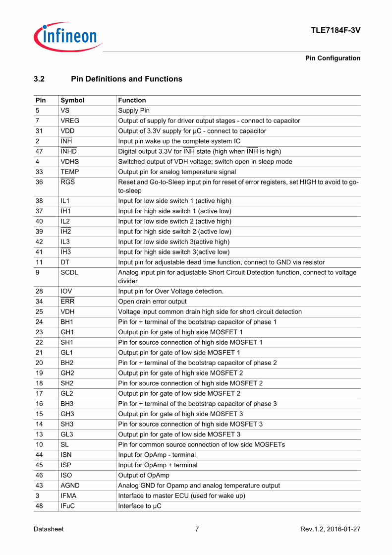
3.2 Pin Definitions and Functions
Pin Symbol Function5 VS Supply Pin7 VREG Output of supply for driver output stages - connect to capacitor31 VDD Output of 3.3V supply for µC - connect to capacitor2 INH Input pin wake up the complete system IC47 INHD Digital output 3.3V for INH state (high when INH is high)4 VDHS Switched output of VDH voltage; switch open in sleep mode33 TEMP Output pin for analog temperature signal36 RGS Reset and Go-to-Sleep input pin for reset of error registers, set HIGH to avoid to go-
to-sleep38 IL1 Input for low side switch 1 (active high)37 IH1 Input for high side switch 1 (active low)40 IL2 Input for low side switch 2 (active high)39 IH2 Input for high side switch 2 (active low)42 IL3 Input for low side switch 3(active high)41 IH3 Input for high side switch 3(active low)11 DT Input pin for adjustable dead time function, connect to GND via resistor9 SCDL Analog input pin for adjustable Short Circuit Detection function, connect to voltage
divider28 IOV Input pin for Over Voltage detection.34 ERR Open drain error output25 VDH Voltage input common drain high side for short circuit detection 24 BH1 Pin for + terminal of the bootstrap capacitor of phase 123 GH1 Output pin for gate of high side MOSFET 122 SH1 Pin for source connection of high side MOSFET 121 GL1 Output pin for gate of low side MOSFET 120 BH2 Pin for + terminal of the bootstrap capacitor of phase 219 GH2 Output pin for gate of high side MOSFET 218 SH2 Pin for source connection of high side MOSFET 217 GL2 Output pin for gate of low side MOSFET 216 BH3 Pin for + terminal of the bootstrap capacitor of phase 315 GH3 Output pin for gate of high side MOSFET 314 SH3 Pin for source connection of high side MOSFET 313 GL3 Output pin for gate of low side MOSFET 310 SL Pin for common source connection of low side MOSFETs44 ISN Input for OpAmp - terminal45 ISP Input for OpAmp + terminal46 ISO Output of OpAmp 43 AGND Analog GND for Opamp and analog temperature output3 IFMA Interface to master ECU (used for wake up)48 IFuC Interface to µC
Datasheet 7 Rev.1.2, 2016-01-27

TLE7184F-3V
Pin Configuration
Exposed pad to be connected to GND
1 GND Ground pin12 GND Ground pin26 GND Ground pin32 GND Ground pin35 GND Ground pin6 NC connect to GND8 NC connect to GND27 NC connect to GND29 NC connect to GND30 NC connect to GND
Pin Symbol Function
Datasheet 8 Rev.1.2, 2016-01-27
TLE7184F-3V
General Product Characteristics
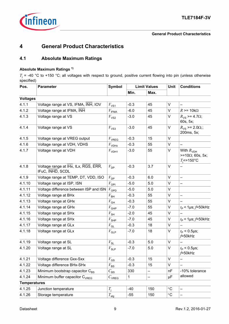
4 General Product Characteristics
4.1 Absolute Maximum Ratings
Absolute Maximum Ratings 1)
Tj = -40 °C to +150 °C; all voltages with respect to ground, positive current flowing into pin (unless otherwisespecified)Pos. Parameter Symbol Limit Values Unit Conditions
Min. Max.Voltages4.1.1 Voltage range at VS, IFMA, INH, IOV VVS1 -0.3 45 V –4.1.2 Voltage range at IFMA, INH VIFMA -6.0 45 V R >= 10kΩ
4.1.3 Voltage range at VS VVS2 -3.0 45 V RVS >= 4.7Ω; 60s, 5x;
4.1.4 Voltage range at VS VVS3 -3.0 45 V RVS >= 2.0Ω;; 200ms, 5x;
4.1.5 Voltage range at VREG output VVREG -0.3 15 V4.1.6 Voltage range at VDH, VDHS VVDHx -0.3 55 V –4.1.7 Voltage range at VDH VVDH1 -3.0 55 V With RVDH
>=10Ω; 60s, 5x;Tj<=150°C
4.1.8 Voltage range at IHx, ILx, RGS, ERR, IFuC, INHD, SCDL
VDP -0.3 3.7 V –
4.1.9 Voltage range at TEMP, DT, VDD, ISO VDP -0.3 6.0 V –4.1.10 Voltage range at ISP, ISN VOPI -5.0 5.0 V –4.1.11 Voltage difference between ISP and ISN VOPD -5.0 5.0 V4.1.12 Voltage range at BHx VBH -0.3 55 V –4.1.13 Voltage range at GHx VGH -0.3 55 V –4.1.14 Voltage range at GHx VGHP -7.0 55 V tP < 1µs; f=50kHz4.1.15 Voltage range at SHx VSH -2.0 45 V –4.1.16 Voltage range at SHx VSHP -7.0 45 V tP < 1µs; f=50kHz4.1.17 Voltage range at GLx VGL -0.3 18 V –4.1.18 Voltage range at GLx VGLP -7.0 18 V tP < 0.5µs;
f=50kHz4.1.19 Voltage range at SL VSL -0.3 5.0 V –4.1.20 Voltage range at SL VSLP -7.0 5.0 V tP < 0.5µs;
f=50kHz4.1.21 Voltage difference Gxx-Sxx VGS -0.3 15 V –4.1.22 Voltage difference BHx-SHx VBS -0.3 15 V –4.1.23 Minimum bootstrap capacitor CBS CBS 330 – nF -10% tolerance
allowed4.1.24 Minimum buffer capacitor CVREG CVREG 1 – µFTemperatures4.1.25 Junction temperature Tj -40 150 °C –4.1.26 Storage temperature Tstg -55 150 °C –
Datasheet 9 Rev.1.2, 2016-01-27

TLE7184F-3V
General Product Characteristics
Note: Stresses above the ones listed here may cause permanent damage to the device. Exposure to absolute maximum rating conditions for extended periods may affect device reliability.
Note: Integrated protection functions are designed to prevent IC destruction under fault conditions described in the data sheet. Fault conditions are considered as “outside” normal operating range. Protection functions are not designed for continuous repetitive operation.
4.2 Functional Range
The limitations in the PWM frequency are given by thermal constraints and limitations in the duty cycle (chargingtime of bootstrap capacitor).All maximum ratings have to be consideredAll basic functions will work between TJ=150°C and Over Temperature shut down. In this temperature range, theparameters might leave the specified range.Note: Within the functional range the IC operates as described in the circuit description. The electrical
characteristics are specified within the conditions given in the related electrical characteristics table.
4.1.27 Case temperature2) TCase – 145 °C –ESD Susceptibility4.1.28 ESD Resistivity3) VESD -2 +2 kV –4.1.29 CDM VCDM – 500 V –1) Not subject to production test, specified by design.2) Calculation based on Tjmax, RthJC and the assumption of 1W power dissipation3) ESD susceptibility HBM according to EIA/JESD 22-A 114B
Pos. Parameter Symbol Limit Values Unit ConditionsMin. Max.
4.2.1 Supply voltage at VS VVS 6.0 45 V below 7V reduced functionality1) 2)
1) MOS driver output deactivated and ERROR pin set to low if VREG is lower UVVR2) MOS driver output stage will operate at Vs=6.7V with 5mA load current at VREG
4.2.2 Quiescent current(IVS + IVDH + IIFMA)
IQ – 50 µA VS<16V;sleep modeVVS=VVDH=VIFMA
4.2.3 Supply current at VS (device enabled)
IVS(0) – 19 mA Vs=8...18V;no load3); fPWM=25kHz;
3) no load at VDD, ERR, ISO, IFµC, VDHS, GXX, TEMP, DT
4.2.4 Duty cycle HS DHS 0 95 % fPWM=20kHz;continuous operation
4.2.5 Duty cycle LS DLS 0 100 %
4.2.6 Junction temperature TJ -40 150 °C –
Absolute Maximum Ratings (cont’d)1)
Tj = -40 °C to +150 °C; all voltages with respect to ground, positive current flowing into pin (unless otherwisespecified)Pos. Parameter Symbol Limit Values Unit Conditions
Min. Max.
Datasheet 10 Rev.1.2, 2016-01-27

TLE7184F-3V
General Product Characteristics
4.3 Thermal ResistanceNote: This thermal data was generated in accordance with JEDEC JESD51 standards. For more information, go
to www.jedec.org.
4.4 Default State of Inputs
Pos. Parameter Symbol Limit Values Unit ConditionsMin. Typ. Max.
4.3.1 Junction to Case1)
1) Not subject to production test, specified by design.
RthJC – – 5 K/W –4.3.2 Junction to Ambient1) RthJA – 29 – K/W 2)
2) Specified RthJA value is according to Jedec JESD51-2,-5,-7 at natural convection on FR4 2s2p board; The Product (Chip+Package) was simulated on a 76.2 x 114.3 x 1.5 mm board with 2 inner copper layers (2 x 70µm Cu, 2 x 35µm Cu). Where applicable a thermal via array under the exposed pad contacted the first inner copper layer.
Table 1 Default State of InputsCharacteristic State RemarkDefault state of ILx (if ILx left open -pull down) Low Low side MOSFETs offDefault state of IHx (if IHx left open - pull up) High High side MOSFETs offDefault state of RGS (if RGS left open - pull down) Low Error signal is reset and
TLE7184F-3V goes to sleep
Default state of INH (if INH left open - pull down) Low no wake up by INHDefault state of SCDL (if SCDL left open - pull up) High Error signal is set; all
MOSFETs switched offDefault state of IFMA (if IFMA left open - pull up)1)
1) external capacitance < 25pF
High no wake up by IFMADefault state of IOV (if IOV left open - pull down) Low no Over Voltage detection
by IOVDefault state of DT (if DT left open) max. dead time max. dead time
Datasheet 11 Rev.1.2, 2016-01-27

TLE7184F-3V
MOSFET Driver
5 MOSFET Driver
5.1 Inputs and Dead TimeThere are 6 independent control inputs to control the 6 MOSFETs individually. However, the control inputs for theHigh Side MOSFETs IHx are inverted. Hence, the control inputs for High Side IHx and Low Side MOSFETs ILx ofthe same half bridge can be tight together to control one half bridge by one control signal. To avoid shoot throughcurrents within the half bridges, a dead time is provided by the TLE7184F-3V. For more details about the dead time please see Chapter 9.2.9
5.2 Output StagesThe 3 low side and 3 high side powerful push-pull output stages of the TLE7184F-3V are all floating blocks.All 6 output stages have the same output power and thanks to the bootstrap principle used, all MOSFETs can beswitched all up to high frequencies.Each output stage has its own short circuit detection block. For more details about short circuit detection seeChapter 9.2.10.1)
Figure 3 Block Diagram of Driver Stages including Short Circuit Detection
1) The high side outputs are not designed to be used for low side MOSFETs; the low side outputs are not designed to be used for high side MOSFETs
GHx
SHx
VDH
VSCP
+
-
Levelshifter
Floating HS driver 3x
GLx
SL
VSCP
+
-
Levelshifter
Floating LS driver 3x
VREG
Voltage regulator BHx
VREG___INHVS
Error logicReset
Power On Reset
____ERR
short circuit filter
SCD SCD
SCD
Input Logic
Shoot ThroughProtection
Dead Time
lock /unlock
___IH1IL1___IH2IL2___IH3IL3
ON / OFF
ON / OFF
GNDDT
Short CircuitDetection Level
____RGS
SCDL
VDH
VREG
blanking
Datasheet 12 Rev.1.2, 2016-01-27
TLE7184F-3V
MOSFET Driver
5.3 Bootstrap PrincipleThe TLE7184F-3V provides a bootstrap based supply for its high side output stages. The benefit of this principleis a fast switching of the high side switches - supporting active freewheeling in high side.The bootstrap capacitors are charged by switching on the external low side MOSFETs connecting the bootstrapcapacitor to GND. Under this condition the bootstrap capacitor will be charged from the VREG capacitor. If the lowside MOSFET is switched off and the high side MOSFET is switched on, the bootstrap capacitor will float togetherwith the SHx voltage to the supply voltage of the bridge. Under this condition the supply current of the high sideoutput stage will discharge the bootstrap capacitor. This current is specified. The size of the capacitor togetherwith this current will determine how long the high side MOSFET can be kept on without recharging the bootstrapcapacitor.When all external MOSFETs are switched off, the SHx voltage can be undefined. Under this condition, thebootstrap capacitors can be discharged, dependent on the SHx voltage.
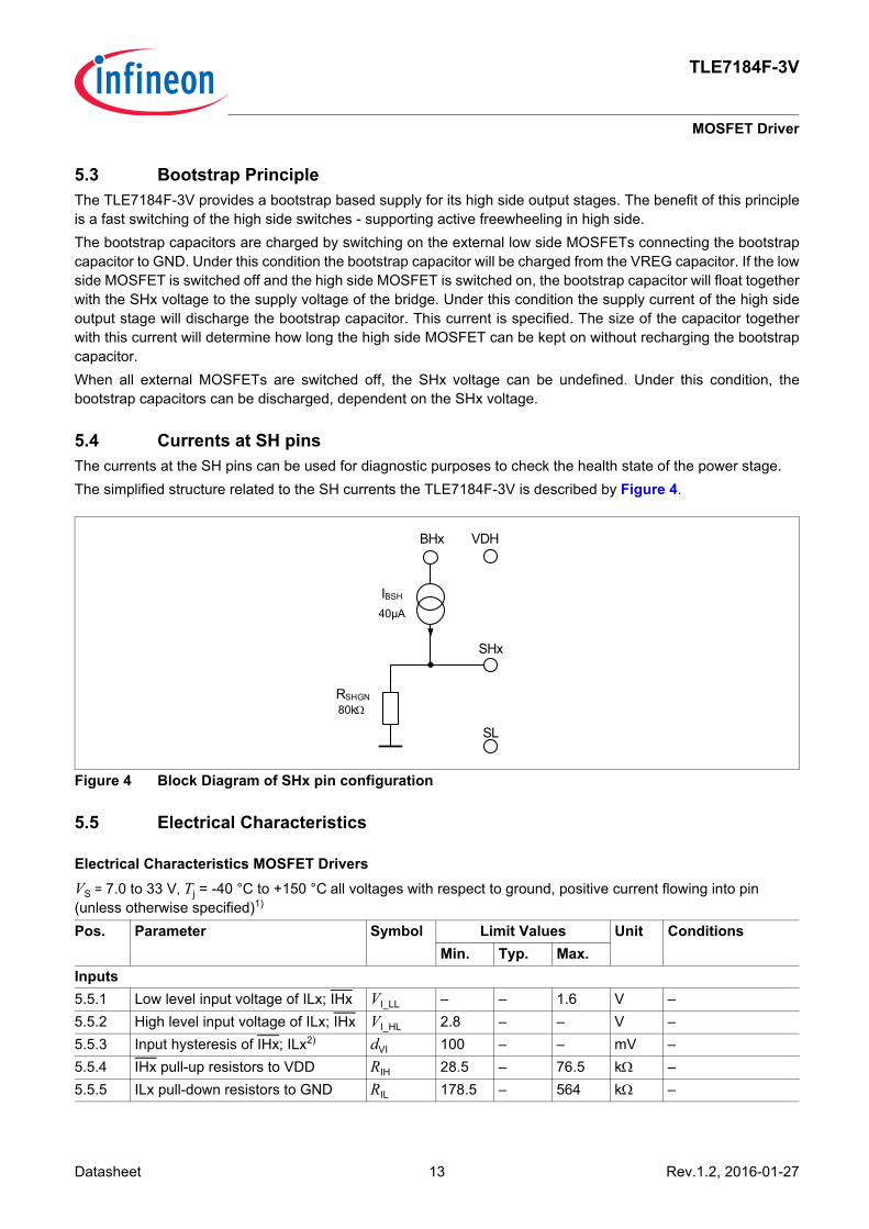
5.4 Currents at SH pinsThe currents at the SH pins can be used for diagnostic purposes to check the health state of the power stage.The simplified structure related to the SH currents the TLE7184F-3V is described by Figure 4.
Figure 4 Block Diagram of SHx pin configuration
5.5 Electrical Characteristics
Electrical Characteristics MOSFET DriversVS = 7.0 to 33 V, Tj = -40 °C to +150 °C all voltages with respect to ground, positive current flowing into pin(unless otherwise specified)1)
Pos. Parameter Symbol Limit Values Unit ConditionsMin. Typ. Max.
Inputs5.5.1 Low level input voltage of ILx; IHx VI_LL – – 1.6 V –5.5.2 High level input voltage of ILx; IHx VI_HL 2.8 – – V –5.5.3 Input hysteresis of IHx; ILx2) dVI 100 – – mV –5.5.4 IHx pull-up resistors to VDD RIH 28.5 – 76.5 kΩ –5.5.5 ILx pull-down resistors to GND RIL 178.5 – 564 kΩ –
VDH
SHx
IBSH
SL
RSHGN
BHx
40µA
80kΩ
Datasheet 13 Rev.1.2, 2016-01-27

TLE7184F-3V
MOSFET Driver
MOSFET driver output5.5.6 Output source resistance RSou 2 – 13.5 Ω Iload=20mA5.5.7 Output sink resistance RSink 2 – 9 Ω Iload=20mA5.5.8 High level output voltage Gxx vs.
SxxVGxx1 – 11 14 V 13,5V
<=VVS<=45V3),VIOV<=VOVIOV,VVDH<=VOVVDHIload=37,5mA
5.5.9 High level output voltage GHx vs. SHx2)
VGxx2 6 – – V VVs=8V, Cload=20nF, dc=95%; fPWM=20kHz
5.5.10 High level output voltage GHx vs. SHx2)4)
VGxx3 6+Vdiode
– – V VVs=8V, Cload=20nF, dc=95%; fPWM=20kHz;passive freewheeling
5.5.11 High level output voltage GLx vs. GND
VGxx4 6.7 – – V VVS=8V, Cload=20nF, dc=95%; fPWM=20kHz;
5.5.12 Rise timeTj = -40°CTj = 150°C
trise100150
––
230350
ns CLoad=11nF;RLoad=1ΩVVS=7V20-80%5.5.13 Fall time
Tj = -40°CTj = 150°C
tfall80150
––
210290
ns
5.5.14 High level output voltage (in passive clamping)
VGUV – – 1.2 V sleep mode or VS_UVLO2) 5)
5.5.15 Pull-down resistor at BHx to GND RBHUV – – 80 kΩ
5.5.16 Pull-down resistor at VREG to GND RVRUV – – 30 kΩ
5.5.17 Bias current into BHx IBH – – 150 µA VBHx-VSHx=5...13V; no switching
5.5.18 Current between BHx and SHx IBSH 15 40 60 µA VBHx-VSHx=5...13V;VSHX = GND
5.5.19 Resistor between SHx and GND RSHGN 48 80 112 kΩ
5.5.20 Bias current out of SL ISL – – 2 mA 0V<=VSH<=VS+1V; no switching; VCBS>5V
Electrical Characteristics MOSFET DriversVS = 7.0 to 33 V, Tj = -40 °C to +150 °C all voltages with respect to ground, positive current flowing into pin(unless otherwise specified)1)
Pos. Parameter Symbol Limit Values Unit ConditionsMin. Typ. Max.
Datasheet 14 Rev.1.2, 2016-01-27

TLE7184F-3V
MOSFET Driver
5.5.21 Input propagation time (low on) tP(ILN) 50 – 200 ns C=11nF; RLoad=1Ω5.5.22 Input propagation time (low off) tP(ILF) 50 – 200 ns
5.5.23 Input propagation time (high on) tP(IHN) 50 – 200 ns5.5.24 Input propagation time (high off) tP(IHF) 50 – 200 ns5.5.25 Absolute input propagation time
difference between above propagation times
tP(diff) – – 100 ns
VREG5.5.26 VREG output voltage VVREG 11 12.5 14 V VVS >= 13,5V;
Iload=37,5mA5.5.27 VREG over current limitation IVREGOCL 100 – 500 mA no activation of
error; VVREG>VVRSD
5.5.28 Voltage drop between Vs and VREG
VVsVREG – – 0.5 V VVS>= 7V;Iload=37,5mA;Ron operation
1) RLoad and CLoad in series2) Not subject to production test; specified by design3) Values above 33V not subjected to production test; specified by design4) Vdiode is the bulk diode of the external low side MOSFET5) see Chapter 9.2.14
Electrical Characteristics MOSFET DriversVS = 7.0 to 33 V, Tj = -40 °C to +150 °C all voltages with respect to ground, positive current flowing into pin(unless otherwise specified)1)
Pos. Parameter Symbol Limit Values Unit ConditionsMin. Typ. Max.
Datasheet 15 Rev.1.2, 2016-01-27

TLE7184F-3V
Shunt Signal Conditioning
6 Shunt Signal ConditioningThe TLE7184F-3V incorporates a fast and precise operational amplifier for conditioning and amplification of thecurrent sense shunt signal. The gain of the OpAmp is adjustable by external resistors within a range higher than 5.The usage of high gains in the application might be limited by required settling time and band width.It is recommended to apply a small offset to the OpAmp, to avoid operation close to the lower rail at low currents.The output of the OpAmp ISO is not short-circuit proof.In addition to the integrated operational amplifier, the TLE7184F-3V incorporates a comparator to detect overcurrent situations. The output voltage VISO is compared to a reference voltage VOCTH close to the upper rail of the3.3V OpAmp supply (VDD). If VISO reaches this level an error is set.
Figure 5 Shunt Signal Conditioning Block Diagram and Over Current Limitation
Over current shut down see Chapter 9.2.12.
6.1 Electrical CharacteristicsElectrical Characteristics - Current sense signal conditioningVS = 6.0 to 33 V, Tj = -40 °C to +150 °C, gain = 5 to 75, all voltages with respect to ground, positive current flowinginto pin (unless otherwise specified)1)
Pos. Parameter Symbol Limit Values Unit ConditionsMin. Typ. Max.
6.1.1 Series resistors RS 100 500 1000 Ω –6.1.2 Feedback resistor
Limited by the output voltage dynamic range
Rfb 2000 7500 – Ω –
6.1.3 Resistor ratio (gain ratio),max. gain limited by settling time
Rfb/RS 5 – – – RL>3kΩ;
6.1.4 Input differential voltage (ISP - ISN) VIDR -800 – 800 mV –6.1.5 Input voltage (Both Inputs - GND)
(ISP - GND) or (ISN -GND)VLL -800 – 800 mV –
6.1.6 Input offset voltage of the I-DC link OpAmp, including temperature drift
VIO – – +/-2 mV RS=500Ω; VCM=0V; VISO=1.65V;
external
RS1
RS2
ASICinternal
-
+
VOCTHERR
Rfb2
Rfb1
Rshunt
VDD
Rfb3
ISN
ISPISO
VDD
-
+
Rfb2 Rfb3 = Rfb1
µC
fc < 1 Mhz
330pF
Datasheet 16 Rev.1.2, 2016-01-27

TLE7184F-3V
Shunt Signal Conditioning
6.1.7 Input bias current (ISN,ISP to GND)
IIB -300 – – µA VCM=0V; VISO=open
6.1.8 High level output voltage of ISO VOH VVDD-0.22
– VVDD V IO=-3mA
6.1.9 Low level output voltage of ISO VOL -0.1 – 0.22 V IO=3mA6.1.10 Guaranteed output current
capabilityIGOC 5 – – mA –
6.1.11 Differential input resistance2) RI 100 – – kΩ –6.1.12 Common mode input capacitance2) CCM – – 10 pF 10kHz6.1.13 Common mode rejection ratio at
DCCMRR = 20*Log((Vout_diff/Vin_diff) * (Vin_CM/Vout_CM))
CMRR 75 100 – dB –
6.1.14 Common mode suppression3)2) with CMS = 20*Log(Vout_CM/Vin_CM)Freq =100kHzFreq = 1MHzFreq = 10MHz
CMS –
624333
– dB VIN=360mV*sin(2*π*freq*t); Rs=500Ω; Rfb=7500Ω
6.1.15 Slew rate dV/dt – 10 – V/µs Gain>= 5;RL=3kΩ; CL=500pF
6.1.16 Large signal open loop voltage gain (DC)
AOL 75 100 – dB –
6.1.17 Unity gain bandwidth GBW 10 20 – MHz RL=3kΩ; CL=100pF6.1.18 Phase margin 2) FM – 50 – ° Gain>= 5;
RL=3kΩ; CL=100pF6.1.19 Gain margin 2) AM – 12 – dB RL=3kΩ; CL=100pF6.1.20 Bandwidth BWG 1.3 – – MHz Gain=15;
RL=3kΩ; CL=500pF; Rs=500Ω
6.1.21 Output settle time to 98%Rfb/RS=15Rfb/RS=75
tset1––
14.6
1.88
µs RL=3kΩ;CL=500pF;0.3<VISO< VDD-0.3V;Rs=500Ω
1) A minimum capacitance of 100pF is needed at the output of the OpAmp (parasitic or real capacitor); RL is the total load resistance including the feedback network; In the application it is not recommended to apply a resistor from the output ISO to GND directly in addition to the feedback network.
2) Not subject to production test; specified by design3) Without considering any offsets such as input offset voltage, internal mismatch and assuming no tolerance error in external
resistors.
Electrical Characteristics - Current sense signal conditioning (cont’d)
VS = 6.0 to 33 V, Tj = -40 °C to +150 °C, gain = 5 to 75, all voltages with respect to ground, positive current flowinginto pin (unless otherwise specified)1)
Pos. Parameter Symbol Limit Values Unit ConditionsMin. Typ. Max.
Datasheet 17 Rev.1.2, 2016-01-27

TLE7184F-3V
3.3 V Low Drop Voltage Regulator
7 3.3 V Low Drop Voltage RegulatorThe TLE7184F-3V incorporates a 3.3V LDO for µC supply. The voltage regulator is protected against OverTemperature by the central temperature sensor (see Chapter 9.2.1 and Chapter 9.2.2). It has an integratedcurrent limitation and Under Voltage detection.Parameters for Under Voltage detection see Chapter 9.2.4.
Figure 6 Block diagram of 3.3V LDO
7.1 Electrical Characteristics
Electrical Characteristics - Current sense signal conditioningVS = 6.0 to 45 V, Tj = -40 °C to +150 °C, all voltages with respect to ground, positive current flowing into pin(unless otherwise specified)Pos. Parameter Symbol Limit Values Unit Conditions
Min. Typ. Max.7.1.1 Output voltage VDD1 3.15 3.35 3.53 V 2mA <=Iload<=70mA;
Cload= 1...22uF1)
1) ceramic C with 100nF with ESR<0.1Ω in parallel
7.1.2 Output voltage VDD2 3.2 3.35 3.5 V 5mA <=Iload<=25mA;Cload= 1...22uF1)
7.1.3 LDO over current limitation IOCL 130 – 270 mA no activation of error by current limitation
7.1.4 Load regulation DVDD – 50 100 mV load step 0...20mA; CVDD=1uF
7.1.5 Power supply ripple rejection2)
2) Not subject to production test; specified by design
PSRR 50 – – dB 100Hz sine wave; 0.5VppVVS>=7V
7.1.6 Power supply ripple rejection2) PSRR – 31 – dB 100Hz sine wave; 0.5Vpp6V<=VVS<7V
3.3V LDO
VDD
Error logic and Wake-up logic
temperature sensor
VS
Datasheet 18 Rev.1.2, 2016-01-27

TLE7184F-3V
3.3 V Low Drop Voltage Regulator
Figure 7 Typ. VDD output voltage vs. load current
Figure 8 Typ. VDD output voltage vs. supply voltage
3,3
3,32
3,34
3,36
3,38
3,4
3,42
3,44
3,46
0 0,01 0,02 0,03 0,04 0,05 0,06 0,07 0,08
U_V
DD
[V]
I_VDD [A]
+150°C+25°C-40°C
3,28
3,3
3,32
3,34
3,36
3,38
3,4
3,42
3,44
0 10 20 30 40 50
U_V
DD
[V]
U_VS [V]
25°C
Datasheet 19 Rev.1.2, 2016-01-27

TLE7184F-3V
Interface, VDH Switch and INH Digital Output
8 Interface, VDH Switch and INH Digital Output
8.1 PWM Interface (IFMA)The TLE7184F-3V has an integrated interface supporting the typical PWM interface between a remote masterECU and the µC. The link to the external master ECU is a single wire communication based on the battery voltageand running typ. with about 10 to 400 Hz. The information is encoded in the duty cycle of the signal. This communication line requires a signal conditioning to connect to the on board µC. The integrated circuit supports the incoming data path.The outgoing data path is formed by external components
Figure 9 Structure PWM Interface
The integrated circuitry is described in Figure 9.The main task of this interface is level shifting and protection of the µC. The IFuC signal is following the IFMA signal, passing the duty cycle information from IFMA to the IFuC.The µC port is used as input and is listening to the IFuC signal. The voltage at IFMA is monitored. If IFMA is lowthe IFuC open drain output is switched on - forcing the IFuC signal to low.If IFMA is high, the IFuC open drain output is deactivated and the IFuC signal is pulled to high by the internal pull-up resistor.The IFMA input is used as well for wake-up. See Chapter 9.1
Influence of serial resistor at IFMA pinAs shown in Figure 9 a 10k resistor R1 is recommended to protect the IFMA pin against negative voltage levelscoming from the interface signal. The integrated pull down and pull up resistors at the IFMA pin form an voltagedivider together with the resistor R1. This will influence the resulting switching level of the IFMA interface in theapplication compared to the levels specified directly at the IFMA pin.In this datasheet an additional parameter is provided to calculate the influence of the 10k resistor. The specifiedIFMA input current divided by Vs allows to calculate the drop over R1 with the following formula:
uC
Interface_uC
GND
TLE 7184 F
KL 30
Pull up
interface ECU
T3
T1
VDD
VCC
IFuCIFMA
T2
Wake up
R110k
VS VS
700k
340k
1**1___ RVVIRoverdropVoltage VS
VS
IFMA=
Datasheet 20 Rev.1.2, 2016-01-27

TLE7184F-3V
Interface, VDH Switch and INH Digital Output
8.2 VDHS SwitchThe System IC has an integrated switch connecting the VDH pin to the VDHS pin. This allows to place an externalvoltage divider for VDH voltage monitoring at the VDHS pin and to disconnect this voltage divider from VDH duringsleep mode to assure low current consumption. The VDHS switch is only deactivated when the VDD regulator isswitched off.
8.3 Digital Output INHDThe System IC provides a digital output INHD showing the logic state of INH (e.g. KL15) after a complete wake-up of the driver (approx. 1ms). The input levels of INH for the INHD output are defined separately from the levelsfor wake-up. Voltage levels for INH wake-up function please see Chapter 9.4 section Wake-up and go-to-sleep.The output stage consists of an integrated low side switch with a pull-up resistor to VDD.
8.4 Electrical Characteristics
Electrical Characteristics - Protection and diagnostic functions
VS = 6.0 to 20V, Tj = -40 °C to +150 °C, all voltages with respect to ground, positive current flowing into pin(unless otherwise specified)Pos. Parameter Symbol Limit Values Unit Conditions
Min. Typ. Max.Interface - static parameters8.4.1 IFMA input voltage high level
(for IFµC high)VIMHL 59 – – % of VVS; IC not in
Sleep Mode8.4.2 IFMA input voltage low level
(for IFµC low)VIMLL – – 46 % of VVS; IC not in
Sleep Mode;8.4.3 IFMA input hysteresis
(for IFµC)VIMhy 0.5 – 9 % of VVS; IC not in
Sleep Mode8.4.4 IFMA wake up voltage high level
= VS-VIFMA
VIMWH 2 – 4 V valid in Sleep Mode
8.4.5 IFMA low time to guarantee wake up
tIFlow 100 – – µs VVS=7...20V
8.4.6 IFMA internal pull-up resistor to VS RIMu 210 340 495 kΩ –8.4.7 IFMA internal pull-down resistor to
GNDRIMd 420 700 980 kΩ not active in Sleep
Mode8.4.8 IFMA input current related to VS
VIFMA = 59% of VVSVIFMA = 46% of VVS
IIFMA/VVS-2.0-3.0
––
+2.0+1.0
µA/V –
8.4.9 IFµC output low voltage VIuLL – – 0.5 V no external load8.4.10 IFµC internal pull-up resistor to VDD RIu 8.5 – 23 kΩ –Interface - dynamic parameters8.4.11 IFµC duty cycle dIu 0 – 100 % –8.4.12 Propagation time rising edge IFµC tPRE – – 6 µs Including rise time
to 80% of VVDD; Cload=100pF
8.4.13 Propagation time falling edge IFµC tPFE – – 5 µs Including fall time to 20% of VVDD; Cload=100pF
Datasheet 21 Rev.1.2, 2016-01-27

TLE7184F-3V
Interface, VDH Switch and INH Digital Output
8.4.14 Deviation between rising and falling IFµC
tPD – – 4 µs Cload=100pF
VDH switch8.4.15 Ron VDH switch RVDH – – 150 Ω Load current = 1mAINHD digital output8.4.16 Low level input voltage INH
(for INHD=low)VINHDL – – 1.5 V –
8.4.17 High level input voltage INH (for INHD=high)
VINHDH 2.2 – – V –
8.4.18 Input hysteresis of INH for INHD1) dVINHD 100 – – mV –8.4.19 INHD low level output voltage VINHD – – 0.5 V no external load8.4.20 INHD Internal pull-up resistor to
VDD
RINHD 42.5 – 115 kΩ –
1) Not subject to production test; specified by design
Electrical Characteristics - Protection and diagnostic functions (cont’d)
VS = 6.0 to 20V, Tj = -40 °C to +150 °C, all voltages with respect to ground, positive current flowing into pin(unless otherwise specified)Pos. Parameter Symbol Limit Values Unit Conditions
Min. Typ. Max.
Datasheet 22 Rev.1.2, 2016-01-27

TLE7184F-3V
Description of Modes, Protection and Diagnostic Functions
9 Description of Modes, Protection and Diagnostic Functions
9.1 Description of modesThe operation of TLE7184F-3V can be described by different operation modes
Figure 10 State diagram TLE7184F-3V
Sleep Mode
- low quiescent current- all supplies switched off
Wake-up Mode
- ramp-up of int5V, VREG and VDD
Error Mode
- latched error is reported- MOSFets switched-off - VREG and VDD on
Normal Modewithout
Error Conditions
- no error is reported- driver stages are active
VREG Shut-down Mode
- latched error is reported- MOSFets switched-off - VREG off
Deadlock Mode*2)
- VREG and VDD off- latched error is reported- MOSFets switched-off - only 5Vint supply is on
/INH = High“OR”
IFMA= Low
Wake-up timeexpired
Reset of error
/RGS = Lowfor t > tsleep
VDD <= VDDsleep
VDD_UVSD
VREG_UVSD
VDD_UVSD
VREG_UVSD
Error condition occures*1)
/RGS = Low for t > tsleep
Error conditions TLE7184F-3V and used abbreviations:
VREG Under Voltage Diagnosis ( VREG_UVD)VDD Under Voltage Diagnosis ( VDD_UVD)Over Current Shut Down ( OCSD)VDH Over Voltage Shut Down ( VDH_OVSD)IOV Over Voltage Shut Down ( IOV_OVSD))Short Circuit Detection ( SCD)SCDL Pin Open Detection ( SCDLPOD)
Over Temperature Shut Down ( OTSD)
VDD Under Voltage Shut Down ( VDD_UVSD) VREG Under Voltage Shut Down ( VREG_UVSD)
VS Under Voltage Lockout ( VS_UVLO)
*1) Error conditions:VREG_UVD, VDD_UVD, OCSD, VDH_OVSD, IOV_OVSD, SCD, SCDLPOD
*2) only way to leave this mode is VS_UVLO
VS Under Voltage Lockout ( VS_UVLO) leads from every mode into the Sleep Mode
Over Temperature Shut Down ( OTSD) leads from every mode except Dead Lock Mode into the Sleep Mode
VDD_UVSD
Go-to-Sleep Mode
- VDD andVREG are switched off- latched error is reported
Datasheet 23 Rev.1.2, 2016-01-27

TLE7184F-3V
Description of Modes, Protection and Diagnostic Functions
Sleep Mode:The sleep mode is entered if the device is in the Go-to-sleep Mode and the VDD voltage is lower than VDDsleep.The complete chip is deactivated beside the wake-up function (see Wake-up Mode). This mode is designed forlowest current consumption from the power net of the car. The passive clamping is active. For details see thedescription of passive clamping, see Chapter 9.2.14.The only way to leave the Sleep Mode is to go to the Wake-up Mode.
Wake-up Mode:The TLE7184F-3V wakes up if INH (=KL15) is high or if IFMA is low and VVS is higher than VVSLO. In this mode all supplies are ramping up. As soon as the internal 5V is available, a so called wake-up timer startsto run. If the IC reaches this state, the wake-up will continue even if the wake-up signals at INH or IFMA disappear.The PWM interface (IFMA) is active as soon as the VDD voltage is sufficiently high. During this time it is expectedthat the supplies are powered up and the µC sets the RGS to high. All external MOSFETs are switched off activelyor passively. When the wake-up timer is expired the IC goes into the Error mode.In this mode all errors will be ignored beside Over Temperature Shut Down or VS Under Voltage Lockout.
Error ModeThe Error Mode can be reached in 2 different ways:1. The device is in Wake-up Mode and the wake-up timer expires2. The device is in Normal Mode and one or more of the following errors occur: VREG Under Voltage Shut Down,
VDD Under Voltage Shut Down, Over Current Shut Down, VDH Over Voltage Shut Down, IOV Over Voltage Shut Down, Short Circuit Detection or SCDL Open Detection.
In this mode an Error is set at the ERROR Pin and all external MOSFETs are actively switched off as long as thebootstrap voltages allows it. The interface is active. VDHS switch is on and the current sense functions areworking. VDD and VREG are active. Passive clamping is not active.The Error mode can be left in the following ways:1. If no error is present, the IC can be sent to Normal Mode by a reset with the RGS pin.2. If a VREG Under Voltage Shut Down occurs the device will go to VREG Shut-down Mode.3. If VDD Under Voltage Shut Down occurs the device will go into Deadlock Mode.
Normal ModeThe Normal Mode can be reached by:1. The device is in Error Mode, no error is present and a reset is performed by the RGS pin.In the Normal Mode all functions are active and available with the regular limitations of the bootstrap principle. Thegate drive output stages can be controlled with the input pins. The Normal Mode can be left in 4 ways:1. The devices goes to the Go-To-Sleep Mode by setting RGS to low for a time longer than tsleep.2. If a VREG Under Voltage Shut Down occurs the device will go to VREG Shut-down Mode.3. If VDD Under Voltage Shut Down occurs the device will go into Deadlock Mode.4. If one or more of the following errors occur, the device goes to the Error Mode: VREG Under Voltage Shut
Down, VDD Under Voltage Shut Down, Over Current Shut Down, VDH Over Voltage Shut Down, IOV Over Voltage Shut Down, Short Circuit Detection or SCDL Open Detection.
Go-To-Sleep ModeThe Go-To-Sleep Mode can be reached in 2 different ways:1. The device is in Normal Mode and RGS is set to low for a time longer than tsleep.2. The device is in VREG Shut-down Mode and RGS is set to low for a time longer than tsleep.
Datasheet 24 Rev.1.2, 2016-01-27

TLE7184F-3V
Description of Modes, Protection and Diagnostic Functions
In this mode all external MOSFETs are actively or passively switched off. An Error is set and is shown as long asVDD is sufficient high. In this mode VDD and VREG is switched off. As soon as VDD voltage reaches the VVDDsleeplevel the IC goes into the Sleep Mode.
Deadlock ModeThis mode is intended to prevent the IC for long time toggling in Over Temperature if a short is present at the VDDpin.There are 3 ways to enter this mode:1. The IC is in Error Mode and a VDD Under Voltage Shut Down occurs. 2. The IC is in Normal Mode and a VDD Under Voltage Shut Down occurs. 3. The IC is in VREG Shut Down Mode and a VDD Under Voltage Shut Down occurs.In this mode VDD and VREG regulators are switched off. The gates of the external MOSFETs are passivelyclamped.The VDHS switch is deactivated.The IC will not react to IFMA or INH signals. Even a Over Temperature Shut Down detection will have no influence.The internal logic is supplied and prevents the IC from going into “Go-to-Sleep Mode”.The only way to leave this state is that VS is lower than VVSLO, means a VS Under Voltage Lockout occurs. In thiscase the IC goes to Sleep Mode.
VREG Shut Down ModeThis mode is intended to prevent the IC from long time toggling in Over Temperature if a short is present at theVREG pin.There are 2 ways to enter this mode:1. The IC is in the Error Mode and a VREG Under Voltage Shut-down occurs.2. The IC is in the Normal Mode and a VREG Under Voltage Shut-down occurs.In this mode VREG is switched off, but VDD is still present. The VDHS switch is still active and the PWM interface(IFMA) is working.The IC will not react to IFMA or INH signals. In this situation the µC is still able to provide diagnostic information by the interface. It can prevent the IC from Go-to-Sleep Mode and can avoid unintended toggling as long there is no Over Temperature Shut Down.This state can be left by 2 ways:1. The µC has to set RGS to low for a time longer than tsleep. In this case the IC goes to Sleep Mode.2. If a VDD Under Voltage Shut Down occurs the IC will go into the Deadlock Mode.
9.2 Protection and Diagnosis Functions
9.2.1 Over Temperature Shut Down (OTSD)If the junction temperature is exceeding the Over Temperature shut down level an error signal is set. The driverIC will pull down the gate-source voltage of all external MOSFETs, deactivate the VDD and VREG supply and godirectly into the Sleep Mode. In the Sleep Mode the regular wake-up conditions will be used. Over Temperature cycling is possible and will leadto accelerated aging of the IC.In Deadlock Mode an Over Temperature Shut Down is ignored.
Datasheet 25 Rev.1.2, 2016-01-27

TLE7184F-3V
Description of Modes, Protection and Diagnostic Functions
9.2.2 Analog Temperature MonitoringThe TEMP output of the TLE7184F-3V provides an analog voltage signal proportional to the chip temperature.This function is not available in Deadlock Mode.
9.2.3 VS Under Voltage Lockout (VS_UVLO)The TLE7184F-3V has an integrated VS Under Voltage Lockout to assure that the behavior of the complete IC ispredictable in all supply voltage ranges.If the supply voltage at VS reaches the Under Voltage shut down level VVSLO for a minimum specified filter timethe IC goes into Go-to-Sleep Mode and finally into Sleep Mode.
9.2.4 VDD Under Voltage Diagnosis (VDD_UVD)The TLE7184F-3V has an integrated VDD Under Voltage Diagnosis to assure that the behavior of the bridge driveroutput stages is predictable in all supply voltage ranges.If the voltage at VDD reaches the Under Voltage diagnosis level VUVVDD for a minimum specified filter time, an erroris set and the IC goes into Error Mode.
Figure 11 Timing of VDD Under Voltage Diagnosis
9.2.5 VDD Under Voltage Shut Down (VDD_UVSD)The TLE7184F-3V has an integrated VDD Under Voltage Shut Down to avoid operation with VDD shorted to GND.If the supply voltage at VDD reaches the Under Voltage shut down level VVDDsleep and the wake-up time is expired,VREG and VDD will be switched off and the IC will go to the Deadlock Mode.
VVDD
VRT
ERRTRR
VS
< TRR
____RGS
Datasheet 26 Rev.1.2, 2016-01-27

TLE7184F-3V
Description of Modes, Protection and Diagnostic Functions
9.2.6 VREG Under Voltage Diagnosis (VREG_UVD)The TLE7184F-3V has an integrated VREG Under Voltage Diagnosis to assure that the behavior of the bridgedriver output stages is predictable in all supply voltage ranges.If the voltage at VREG reaches the Under Voltage diagnosis level VUVVR for a minimum specified filter time an erroris set the IC goes into Error Mode. As long as the VS Under Voltage Lock Out is not reached, the low side MOSFETs will stay actively switched off.The status of the high side MOSFET drivers is dependent on the bootstrap voltage - which depends on the SHxvoltage. It is expected that the SHx nodes will be pulled to VDH level by the high side MOSFETs and this will switchoff the high side MOSFETs passively.In this situation the short circuit detection of this output stage is deactivated to avoid wrong error reporting.
9.2.7 VREG Under Voltage Shut Down (VREG_UVSD)The TLE7184F-3V has an integrated VREG Under Voltage Shut Down to avoid operation with VREG shorted toGND.If the supply voltage at VREG reaches the Under Voltage shut down level VVRSD “AND” the wake up time isexpired, VREG will be switched off and the IC will go to the VREG Shut Down Mode. In this condition the µC isstill supplied and can communicate via the PWM interface (IFMA), the MOSFETs are switched off and an error isset. The only way to leave this mode is to go to “Sleep Mode”.
9.2.8 IOV and VDH Over Voltage Shut Down (IOV_OVSD, VDH_OVSD)The TLE7184F-3V has an integrated Over Voltage shut down to minimize the risk of destruction of the IC at highsupply voltages caused by violation of the maximum ratings.The voltages are observed at the Over Voltage input pin IOV and at the VDH pin. If the voltage at the IOV pin orat the VDH pin exceeds the Over Voltage shut down level for more than the specified filter time, the IC goes intoError Mode.The effective Over Voltage level can be adjusted by a voltage divider at the IOV pin. This voltage devider isnormally supplied by the VDHS pin. The Over Voltage level at VDH is fix.
9.2.9 Dead Time and Shoot Through ProtectionIn bridge applications it has to be assured that the external high side and low side MOSFETs are not “on” at thesame time, connecting the battery voltage directly to GND. The dead time generated in the TLE7184F-3V is setto a minimum value if the DT pin is connected to GND. This function assures a minimum dead time if a commoninput signal for ILx and IHx is used.The dead time can be increased by connecting the DT pin via a dead time resistor RDT to GND. Larger dead timeresistors result in a longer dead time.The typical dead time can be calculated with the following formula:
Please put in the Rdt in kΩ.
If an exact dead time of the bridge is needed, the use of the µC PWM generation unit is recommended.In case of an open DT pin, the dead time is set to the internal maximum value.In addition to this dead time, the TLE7184F-3V provides a locking mechanism avoiding that both externalMOSFETs of one half bridge can be switched on at the same time. This functionality is called shoot throughprotection.
µstRdt
deadtime++
=4
4.202.0081.0
Datasheet 27 Rev.1.2, 2016-01-27

TLE7184F-3V
Description of Modes, Protection and Diagnostic Functions
If the command to switch on both high and low side switches in the same half bridge is given at the input pins, thecommand will be ignored. The outputs will stay in the state like before the conflicting input.
9.2.10 Short Circuit Protection (SCP)The TLE7184F-3V provides a short circuit protection for the external MOSFETs. It is monitoring of the drain-sourcevoltage of the external MOSFETs. (see Figure 3 )The drain-source voltage monitoring for a certain external MOSFET is active as soon as the corresponding driveroutput stage is set to “on” and the dead time and the blanking time is expired.The blanking time starts when the dead time is expired and assures that the switch on process of the MOSFET isnot taken into account. It is recommended to keep the switching times of the MOSFETs below the blanking time.The short circuit detection level is adjustable in an analogue way by the voltage setting at the SCDL pin. There isa 1:1 translation between the voltage applied to the SCDL pin and the drain-source voltage limit. E.g. to trigger theSCD circuit at 1 V drain-source voltage, the SCDL pin must be set to 1 V as well. The drain-source voltage limitcan be chosen between 0.3 ... 2 V.In the case that after the expiration of the blanking time the drain source voltage of the observed MOSFET is stillhigher then the SCDL level, the SCD filter time tSCP starts to run. A capacitor is charged with a current. If thecapacitor voltage reaches a specific level (filter time tSCP), the error signal is set and the IC goes into Error Mode.If the SCD condition is removed before the SC is detected, the capacitor is discharged with the same current. Thedischarging of the capacitor happens as well when the MOSFET is switched off. It has to be considered that thehigh side and the low side outputs of one phase are working with the same capacitor.
9.2.11 SCDL Pin Open Detection (SCDL_open)For safety reasons a pull-up resistor at the SCDL pin assures that in case of an open pin the SCDL voltage ispulled to a high level. In this case an error is set and the IC goes into Error Mode.
9.2.12 Over Current Shut Down (OCSD)The TLE7184F-3V is monitoring the output signal of the operational amplifier. If the output signal reaches aspecified level close to the upper rail (VDD) for a specified time, the System IC detects an over current conditionand sets an error signal. The driver output pulls down the gate-source voltage of all external MOSFETs activelyand stays in the Error Mode.
9.2.13 VDD Current LimitationThe TLE7184F-3V has an integrated voltage supply for an external µC. The output current of the supply is limitedto a specified value. This limitation does not cause any error reporting. In this situation a VDD Under Voltagedetection is likely. If the current is limited for a longer time, the Over Temperature protection will react.
9.2.14 Passive Gxx ClampingIf VS Under Voltage Lock Out is detected or the device is in Sleep Mode, a passive clamping is active as long asthe voltage at VS or VDH is higher than 3V. Even below 3V it is assured that the MOSFET driver stage will notswitch on the MOSFET actively.The passive clamping means that the BHx and the VREG pin are pulled to GND with specified pull down resistors.Together with the intrinsic diode of the push stage of the output stages which connect the gate output to BHxrespectively VREG, this assures that the gate of the external MOSFETs are not floating.
9.3 ERR PinThe TLE7184F-3V has a status pin to provide diagnostic feedback to the µC. The logical output of this pin is anopen drain output with integrated pull-down resistor to GND (see Figure 12).
Datasheet 28 Rev.1.2, 2016-01-27

TLE7184F-3V
Description of Modes, Protection and Diagnostic Functions
Reset of error registers and DisableThe TLE7184F-3V can be reset by the enable pin RGS. If the RGS pin is pulled to low for a specified minimumtime, the error registers are cleared. If the error is still existing when the RGS pin is pulled to low, no reset will beperformed and the ERR pin stays low.Figure 13 describes the timing behavior during error reset:
Figure 12 Structure of ERR output
Figure 13 Enable / Disable timing
ErrorLogic
uC
Interface_uC
GND
internalVDD
ERR
GND
Error occurs
No driverreset
tnres-min tres-min
undefined
TLE 7184 F releases signal
3.3V
0V
ERR
3.3V
0V
RGS
tsleep
Err reset; Normal operation Sleep mode
Short glitches areignored
____
Datasheet 29 Rev.1.2, 2016-01-27

TLE7184F-3V
Description of Modes, Protection and Diagnostic Functions
9.4 Electrical Characteristics
Electrical Characteristics - Protection and diagnostic functions
VS = 7.0 to 33V, Tj = -40 °C to +150 °C, all voltages with respect to ground, positive current flowing into pin(unless otherwise specified)Pos. Parameter Symbol Limit Values Unit Conditions
Min. Typ. Max.Dead time9.4.1 Programmable internal dead time tDT 0.095
0.290.851.22.1
0.140.421.211.883.62
0.180.551.552.65.1
µs RDT=0 ΩRDT=10 kΩRDT=47 kΩRDT=100 kΩRDT=1000 kΩ
9.4.2 Max. internal dead time tDT_MAX 2.0 4.0 6.0 µs DT pin open9.4.3 Dead time deviation between
channelsdtDT -20 – 20 % –
-15 – 15 % RDT<=47 kΩ
9.4.4 Dead time deviation between channels LSoff -> HS on
dtDTH -14 – 14 % –-12 – 12 % RDT<=47 kΩ
9.4.5 Dead time deviation between channels HSoff -> LS on
dtDTL -14 – 14 % –-12 – 12 % RDT<=47 kΩ
Short circuit protection9.4.6 Short circuit protection detection
levelVSCPDL 0.3 – 2 V programmed by
SCDL pin9.4.7 Short circuit protection detection
AccuracyASCP -20 – +20 % 0.3V<= VSCDL<0.9V
9.4.8 Short circuit protection detection Accuracy
ASCP -10 – +10 % 0.9V<= VSCDL<=2.0V
9.4.9 Filter time of short circuit protection tSCP(off) 2.3 – 4.3 µs Ixx static on9.4.10 Blanking time plus filter time of
short circuit detectiontSCPTT 4 – 8 µs Ixx switching “off” to
“on”9.4.11 Internal pull-up resistor SCDL to
VDD
RSCDL 180 300 420 kΩ –
9.4.12 SCDL open pin detection level VSCPOP 2.0 – 2.5 V –9.4.13 Filter time of SCDL open pin tSCPOP 1 – 3.4 µs –9.4.14 SCDL open pin detection level
hysteresis2)VSCOPH – 0.3 – V –
Over- and Under Voltage monitoring9.4.15 Over Voltage shut down at IOV VOVIOV 4.15 – 4.4 V IOV voltage
increasing9.4.16 Pull down resistor at IOV to GND RIOV 300 – 700 kΩ –9.4.17 Over Voltage shut down at VDH VOVVDH 33 – 37 V VDH increasing9.4.18 Over Voltage shut down filter time
for IOV or VDHtOV 13 – 23 µs –
9.4.19 Under Voltage diagnosis at VREG VUVVR 5.5 – 6.5 V VREG decreasing
Datasheet 30 Rev.1.2, 2016-01-27

TLE7184F-3V
Description of Modes, Protection and Diagnostic Functions
9.4.20 Under Voltage diagnosis filter time for VREG
tUVVR 10 – 30 µs –
9.4.21 Under Voltage shut down at VREG VVRSD 1.5 – 2.3 V VREG decreasing9.4.22 Under Voltage lockout at VS VVSLO 4.4 5.0 5.5 V VVS decreasing9.4.23 Under Voltage lockout filter time for
VStUVLO 1 – 3 µs –
ERR pin1)
9.4.24 ERR output voltage VERR 2.9 – – V No external load9.4.25 Rise time ERR (20 - 80% of internal
5V)tf(ERR) – – 3.5 µs CLOAD=1nF
9.4.26 Internal pull-down resistor ERR to GND
Rf(ERR) 21.2 – 60 kΩ –
Reset and Enable9.4.27 Low time of uC RGS signal without
resettnres – – 0.5 µs –
9.4.28 Low time of uC RGS pin necessary to trigger reset and to clear error registers
tres 3 – – µs –
Wake-up and go-to-sleep9.4.29 Low level input voltage of RGS VRGSLL – – 1.6 V –9.4.30 High level input voltage of RGS VRGSHL 2.8 – – V –9.4.31 Input hysteresis of RGS2) dRGS 100 – – mV –9.4.32 RGS pull-down resistors to GND RRGS 100 – 210 kΩ –9.4.33 Low level input voltage of INH3) for
wake upVINHL – – 0.75 V –
9.4.34 High level input voltage of INH3) for wake up
VINHH 2.1 – – V –
9.4.35 INH high time to guarantee wake-up
VIHhigh 100 – – µs –
9.4.36 INH pull-down resistors to GND RINH 100 – 210 kΩ –9.4.37 Wake up delay time twake 9 – 17 ms9.4.38 RGS low time for go-to-sleep tsleep 20 – 50 µs9.4.39 VDD voltage for changing
from Go-to-Sleep Mode to Sleep Mode
VDDsleep 1.5 – 2.3 V –
9.4.40 VDD Under Voltage Shut Down VUVSDVDD 1.5 – 2.3 V –1) ERR pin and Reset & Enable functional between VVS=6 ... 7V, but characteristics might be out of specified range2) Not subject to production test; specified by design3) These levels are valid for wake up of the IC. The input levels for INH deciding the output state of INHD are shown in
Chapter 8.4
Electrical Characteristics - Protection and diagnostic functions (cont’d)
VS = 7.0 to 33V, Tj = -40 °C to +150 °C, all voltages with respect to ground, positive current flowing into pin(unless otherwise specified)Pos. Parameter Symbol Limit Values Unit Conditions
Min. Typ. Max.
Datasheet 31 Rev.1.2, 2016-01-27

TLE7184F-3V
Description of Modes, Protection and Diagnostic Functions
Electrical Characteristics - Protection and diagnostic functions
VS = 6.0 to 33V, Tj = -40 °C to +150 °C, all voltages with respect to ground, positive current flowing into pin(unless otherwise specified)Pos. Parameter Symbol Limit Values Unit Conditions
Min. Typ. Max.Temperature monitoring9.4.41 Over Temperature shut down Tj(SD) 160 170 180 °C 1)–
9.4.42 Analog temperature output at 25°C VATRT 1.32 – 1.65 V Cload<=1.5nF; Tj=25°C
9.4.43 Analog temperature output coefficient
KATRT 4.57 – 5.20 mV/K Cload<=1.5nF 1)
9.4.44 Analog temperature output drift over lifetime1)
VATRTd 0 – +6 mV Cload<=1.5nF
9.4.45 Analog temperature range1)
1) Not subject to production test; specified by design
TAT -40 – 175 °C –Over current detection9.4.46 Over current detection level in% of
VVDD
VOCTH 92 – 96.5 % –
9.4.47 Filter time for over current detection tOC 1.8 – 4.2 µs –Under Voltage monitoring VDD9.4.48 Under Voltage shut down at VDD
2)
2) For Under Voltage detection level during go-to-sleep see VDDsleep
VUVVDD 2.4 – 2.85 V VVDD decreasing9.4.49 Under Voltage shut down filter time tUVVDD 15 – 45 µs –
Datasheet 32 Rev.1.2, 2016-01-27

TLE7184F-3V
Application Description
Datasheet 33 Rev.1.2, 2016-01-27
10 Application DescriptionIn the automotive sector there are more and more applications requiring high performance motor drives, such asHVAC fans, engine cooling fans, pumps etc.. In these applications 3 phase motors, synchronous andasynchronous, are used, combining high output performance, low space requirements and high reliability.
Figure 14 Application Circuit TLE7184F-3V
Note: This is a simplified example of an application circuit. The function must be verified in the real application
SH1
VBAT
CBR4,7mF
µC
GH1
GL1
VS
IL1___IH1
CVS100 nF
RVS10 Ω
GND
ISP
IL2___IH2
IL3___IH3
GND
VREG
TLE7184
PGND
PGND
____ERRTEMP
ISO
ShuntRS
RS
Rfb1
____RGS____INHD
ISN
BH1 CBS1470nF
RGH1
SH2
GH2
BH2
RGH2
CBS2470nF
SH3
GH3
BH3
RGH3
CBS3470nF
RGL1
GL2RGL2
GL3RGL3
AGND
L2,2µH
IFMA
R1,6kΩ
L2,2µH interface
R33Ω
IFuC
DT
VDD
GND
AGND
AGND
RDT
CLP
SL
CBR1µF
PGND
KL 15
R2,2kΩ
___INH
VDHS
Rfb3
AGND
GND
VDH
CREG2µF
RVDH
+
IOV
SCDL
Rfb2
R1,2kΩ
R10kΩ
TLS2
TLS3
TLS1
THS2
THS3
THS1
RSC1
RSC2
CVDD1100nF
ROV1
ROV2
RVDH1
RVDH2
R10kΩ
CVDD22.2nF
CVS2µF
Rfb2 || Rfb3 = Rfb1
For details of the current sense feature please see the dedicated chapter
AGND
CISO
RLP

Datasheet 34 Rev.1.2, 2016-01-27
TLE7184F-3V
Package Outlines
11 Package Outlines
Figure 15 PG-VQFN-48
Green Product (RoHS compliant)To meet the world-wide customer requirements for environmentally friendly products and to be compliant withgovernment regulations the device is available as a green product. Green products are RoHS-Compliant (i.ePb-free finish on leads and suitable for Pb-free soldering according to IPC/JEDEC J-STD-020).
You can find all of our packages, sorts of packing and others in ourInfineon Internet Page “Products”: http://www.infineon.com/products. Dimensions in mm
TLE7184F-3V
Revision History
Datasheet 35 Rev.1.2, 2016-01-27
12 Revision History
Revision Date ChangesRev.1.2 2016-01-27 - package adjustmentsRev.1.1 2011-08-03 - added figure VDD output voltage vs load current
- added figure VDD output voltage vs supply voltageRev.1.0 2011-04-20 - INH high time to guarantee wake-up added
- IFMA low time to guarantee wake-up added- Text Description improved - remaining OTPW text removed- Steady state differential input voltage range across VIN removed- SCDL open pin detection level hysteresis, footnote added
Rev.0.4 2011-03-17 - Common mode suppression, footnote added- High level input voltage INH (for INHD=high) adapted- SCDL open pin detection level hysteresis, footnote added- Rise time ERR adapted- ERR output voltage adapted- Over temperature pre-warning removed
Rev.0.3 2011-03-14 - Voltage difference between ISP and ISN specified- Minimum buffer capacitor CVREG specified- Description of SH currents added- Pull up and pull down resistors at IHx and ILx expanded- Propagation time tolerance reduced- Rise and fall times specified- Fig. 4 new- Fig. 5 updated- Pull up resistor at INHD expanded- Pull down resistor at ERR output expanded- Pull up resistor at IFuC output expanded- Matching of IFMA pull up / pull down resistors replaced by IFMA input current / VS- Limit the lower load current of VDD to 2mA- Dead time description improved- Short circuit detection accuracy improved- Analog temperature output at 25°C improved

Edition 2016-01-27Published byInfineon Technologies AG81726 Munich, Germany© 2016 Infineon Technologies AGAll Rights Reserved.
Legal DisclaimerThe information given in this document shall in no event be regarded as a guarantee of conditions or characteristics. With respect to any examples or hints given herein, any typical values stated herein and/or any information regarding the application of the device, Infineon Technologies hereby disclaims any and all warranties and liabilities of any kind, including without limitation, warranties of non-infringement of intellectual property rights of any third party.
InformationFor further information on technology, delivery terms and conditions and prices, please contact the nearest Infineon Technologies Office (www.infineon.com).
WarningsDue to technical requirements, components may contain dangerous substances. For information on the types in question, please contact the nearest Infineon Technologies Office.Infineon Technologies components may be used in life-support devices or systems only with the express written approval of Infineon Technologies, if a failure of such components can reasonably be expected to cause the failure of that life-support device or system or to affect the safety or effectiveness of that device or system. Life support devices or systems are intended to be implanted in the human body or to support and/or maintain and sustain and/or protect human life. If they fail, it is reasonable to assume that the health of the user or other persons may be endangered.