awesillo-scope
DESCRIPTION
AWESILLO-SCOPE. Team 2 Yimin Xiao Jintao Zhang Bo Yuan Yang Yang. Overall Description. - PowerPoint PPT PresentationTRANSCRIPT

AWESILLO-SCOPE
Team 2Yimin Xiao
Jintao ZhangBo Yuan
Yang Yang

The project we propose is a digital oscilloscope with playback function that provides almost any function of a typical oscilloscope, such as digital sampling, signal processing, scaling, cursor setting, reconstruction and visualization of signals. Additional features such as recording and replicating signals as a function generator, and write data to external storage (SD card).
Overall Description

Updated Block Diagram

MAIN function Flowchart
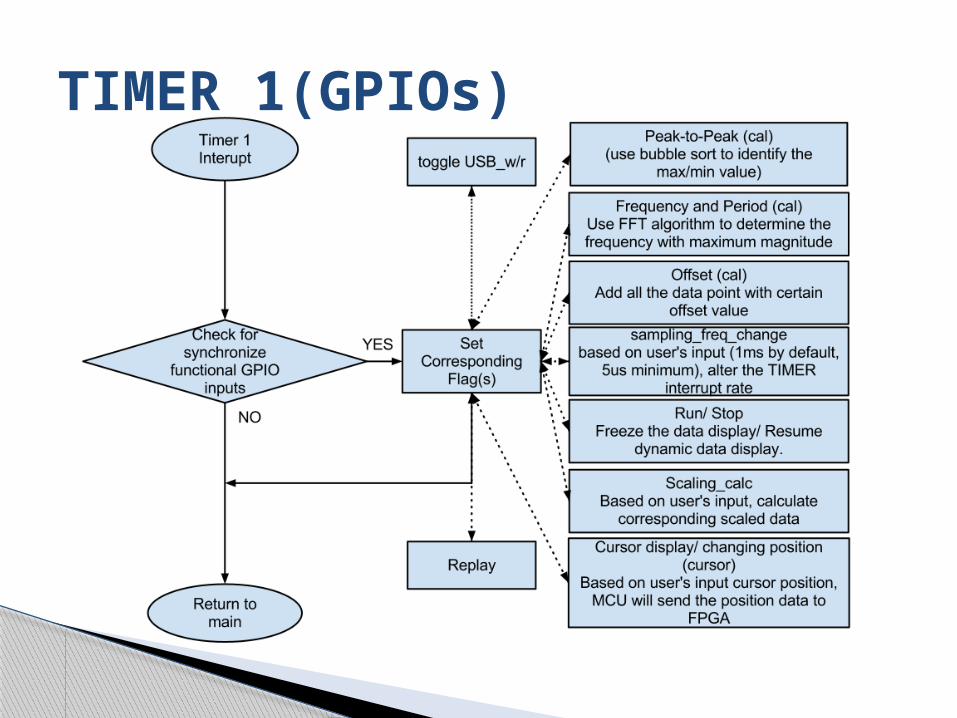
TIMER 1(GPIOs)

TIMER 2 (Transmit Data)
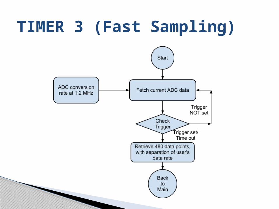
TIMER 3 (Fast Sampling)

TIMER 4 (Slow Sampling)

Self-Timing (auto-sampling at 1.2 MHz frequency)
12 bit data, save 480 points to display for each channel
In Slow Mode, sample_counter + 1 in every TIMER interrupt. If maximized, reset trigger from 1st data
In Fast Mode, set trigger at first, then save 480 data-points with proper delay
◦ Progress: ADC initialization code written, not yet structuralized.
ADC input

MCU serve as Master device and FPGA serve as the only Slave device.
Data rate at 3.4MHz(subject to change) Master transmit data points (480 data points
each channel/display), menu information, calculated result and cursor position to Slave
No meaningful data required from Slave to Master
◦ Progress: Master Code written and tested, Slave code from ECE337 (not tested yet).
I2C Interface

Display in standard mode (standard timing, line-by-line display, etc.)
Use 640 x 480 resolution (correspond to the 480 data points)
Clock at 27.175 MHz Reverse color when menu item is selected
◦ Progress: VGA display and interface tested and fully functional. Code still in progress.
VGA output (on FPGA)

Input: Initialize all the pushbuttons’ state registers, RPGs’ position registers to default
Change the register value accordingly The registers’ value will be displayed on the
output, and will be used to alter the input circuitry
◦ Progress: Not yet started(majorly due to SRAM location)
GP Input (PB, RPG) Output (Circuit)

Use USB-OTG interface on the STM32F4 series Microprocessor
◦ Progress: USB code tested with Logic Analyzer, writing mode functioning properly
DAC implemented to output waveform, the analog circuit will boost it up
◦ Progress: Simple waveform generated, not yet related with sampled data.
USB interface & DAC output

Questions