ax-sigfox · available from axsem for any sigfox ... other parts of the ecosystem include o ready...
TRANSCRIPT
DATASHEET
AX-SIGFOX
Ultra-Low Power, AT Command Controlled, Sigfox Compliant Transceiver IC for Up-Link and Down-Link
Revision 2
www.onsemi.com AX-SIGFOX/D
2
Table of Contents
1. Overview .................................................................................................................. 4
1.1. Circuit description ....................................................................................................... 4
1.2. Features .................................................................................................................... 4
1.3. Applications ............................................................................................................... 5
2. Block Diagram .......................................................................................................... 6
3. Pin Function Descriptions ......................................................................................... 7
3.1. Pinout Drawing ........................................................................................................... 9
4. Specifications ......................................................................................................... 10
4.1. Absolute Maximum Ratings ......................................................................................... 10
4.2. DC Characteristics ..................................................................................................... 11
Supplies .................................................................................................................... 11
Typical Current Waveform ........................................................................................... 12
Battery Life Examples ................................................................................................. 13
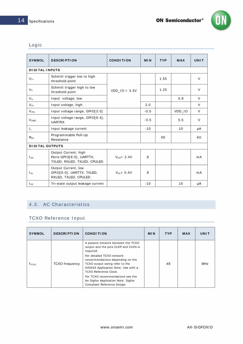
Logic ........................................................................................................................ 14
4.3. AC Characteristics ...................................................................................................... 14
TCXO Reference Input ................................................................................................ 14
Transmitter ............................................................................................................... 15
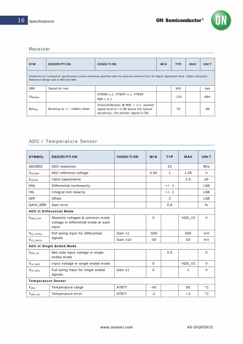
Receiver.................................................................................................................... 16
ADC / Temperature Sensor .......................................................................................... 16
5. Command Interface ............................................................................................... 17
5.1. Serial Parameters: 9600,8,N,1 .................................................................................... 17
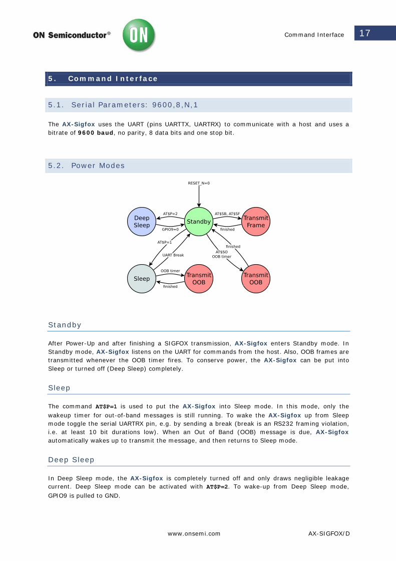
5.2. Power Modes ............................................................................................................. 17
Standby .................................................................................................................... 17
Sleep ........................................................................................................................ 17
Deep Sleep ................................................................................................................ 17
5.3. AT Commands ........................................................................................................... 18
Numerical Syntax ....................................................................................................... 18
Command Syntax ....................................................................................................... 18
Table of Contents
www.onsemi.com AX-SIGFOX/D
3
Return Codes ............................................................................................................. 18
Examples .................................................................................................................. 18
Commands ................................................................................................................ 19
Registers................................................................................................................... 24
6. Application Information ......................................................................................... 25
6.1. Typical Application Diagrams ....................................................................................... 25
Typical Sigfox Application Diagram ............................................................................... 25
7. QFN40 Package Information .................................................................................. 26
7.1. Package Outline QFN40 5x7mm ................................................................................... 26
7.2. QFN40 Soldering Profile .............................................................................................. 27
7.3. QFN40 Recommended Pad Layout ................................................................................ 28
7.4. Assembly Process ...................................................................................................... 28
Stencil Design & Solder Paste Application ...................................................................... 28
8. Device Versions ...................................................................................................... 30
Table of Contents
www.onsemi.com AX-SIGFOX/D
4
1. Overview
1.1. Circuit description
AX-Sigfox is an ultra-low power single chip solution for a node on the Sigfox network with both up- and down-link functionality. The AX-Sigfox chip is delivered fully ready for operation and contains all the necessary firmware to transmit and receive data from the Sigfox network in Europe. It connects to the customer product using a logic level RS232 UART. AT commands are used to send frames and configure radio parameters.
1.2. Features
Functionality and Ecosystem
• Sigfox up-link and down-link functionality controlled by AT commands
• The AX-Sigfox IC is part of a whole development and product ecosystem available from AXSEM for any Sigfox requirement. Other parts of the ecosystem include
o Ready to go AX-Sigfox development kit with fully functional AX-Sigfox module including Sigfox subscription
o Sigfox Ready certified reference design for the AX-Sigfox IC
o PIOX by AXSEM Sigfox modules with SMA connector or chip antenna
o AX-Sigfox-API IC for customers wishing to write their own application software based on the AXSEM Sigfox Library
General Features
• QFN40 4mm x 5mm package
• Supply range 1.8V - 3.6V
• -40°C to 85°C
• Temperature sensor
• Supply voltage measurements
• 10 GPIO pins
o 4 GPIO pins with selectable voltage measure functionality, differential
(1V or 10V range) or single ended (1V range) with 10 bit resolution
o 2 GPIO pins with selectable sigma delta DAC output functionality
o 2 GPIO pins with selectable output clock
o 3 GPIO pins selectable as SPI master interface
o Integrated RX/TX switching with differential antenna pins
Power Consumption
• Ultra-low power consumption:
o Charge required to send a Sigfox OOB packet at 14dBm output power: 0.28 C
o Deepsleep mode current: 100 nA
o Sleep mode current: 1.3 μA
o Standby mode current: 0.5 mA
o Continuous radio RX-mode at 869.525 MHz : 10 mA
o Continuous radio TX-mode at 868.130 MHz 19 mA @ 0 dBm 49 mA @ 14 dBm
High performance narrow-band Sigfox RF transceiver • Receiver
o Carrier frequency 869.525 MHz
o Data-rate 600 bps
o Sensitivity -126 dBm @ 600bps, 869.525MHz, GFSK
o 0 dBm maximum input power
• Transmitter
o Carrier frequency 868.13 MHz
o Data-rate 100 bps
o High efficiency, high linearity integrated power amplifier
o Maximum output power 14 dBm
o Power level programmable in 1dBm steps

Overview
www.onsemi.com AX-SIGFOX/D
5
1.3. Applications
Sigfox networks up-link and down-link.
Sigfox and Sigfox Ready are registered trademarks of Sigfox SARL.
Block Diagram
www.onsemi.com AX-SIGFOX/D
6
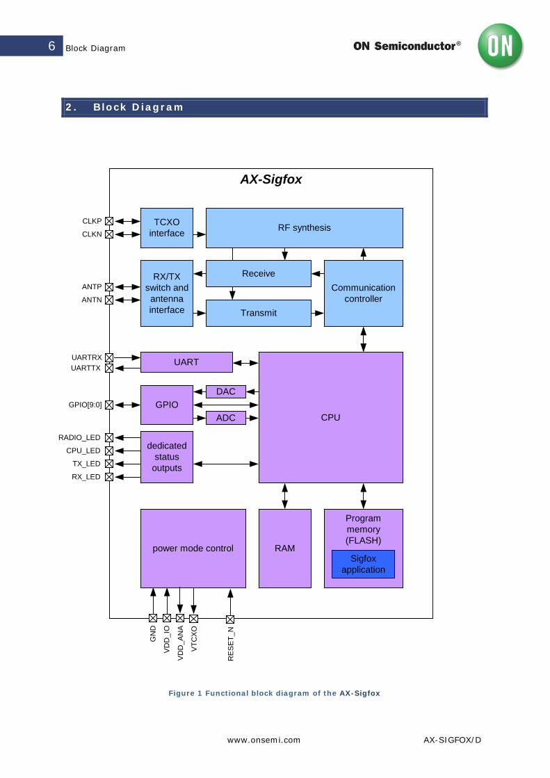
2. Block Diagram
RX/TXswitch andantennainterface Transmit
Communicationcontroller
CPU
Programmemory(FLASH)
Sigfoxapplication
RAMpower mode control
ADCGPIO
UART
RF synthesis
DAC
AX-Sigfox
TCXOinterface
Receive
CLKP
CLKN
ANTP
ANTN
UARTRXUARTTX
GPIO[9:0]
VD
D_I
O
VD
D_A
NA
GN
D
dedicatedstatus
outputs
RADIO_LED
CPU_LED
TX_LED
RX_LED
VTC
XO
RE
SE
T_N
Figure 1 Functional block diagram of the AX-Sigfox
Pin Function Descriptions
www.onsemi.com AX-SIGFOX/D
7
3. Pin Function Descriptions
Symbol Pin(s) Type Description
VDD_ANA 1 P Analog power output, decouple to neighboring GND
GND 2 P Ground, decouple to neighboring VDD_ANA
ANTP 3 A Differential antenna input/output
ANTN 4 A Differential antenna input/output
NC 5 N Do not connect
GND 6 P Ground, decouple to neighboring VDD_ANA
VDD_ANA 7 P Analog power output, decouple to neighboring GND
GND 8 P Ground
FILT 9 A Synthesizer filter
NC 10 A Must be connected to pin 11
NC 11 A Must be connected to pin 10
NC 12 N Do not connect
GPIO8 13 I/O/PU General purpose IO
GPIO7 14 I/O/PU General purpose IO, selectable SPI functionality (MISO)
GPIO6 15 I/O/PU General purpose IO, selectable SPI functionality (MOSI)
GPIO5 16 I/O/PU General purpose IO, selectable SPI functionality (SCK)
GPIO4 17 I/O/PU General purpose IO, selectable Σ∆ DAC functionality, selectable clock functionality
CPU_LED 18 O CPU activity indicator
RADIO_LED 19 O Radio activity indicator
VTCXO 20 O TCXO power
GPIO9 21 I/O/PU General purpose IO, wakeup from deep sleep
UARTTX 22 O UART transmit
UARTRX 23 I/PU UART receive
RX_LED 24 O Receive activity indicator
TX_LED 25 O Transmit activity indicator
NC 26 PD Do not connect
RESET_N 27 I/PU Optional reset pin Internal pull-up resistor is permanently enabled, nevertheless it is recommended to connect this pin to VDD_IO if it is not used.
GND 28 P Ground
VDD_IO 29 P Unregulated power supply
GPIO0 30 I/O/A/PU General purpose IO, selectable ADC functionality, selectable Σ∆ DAC functionality, selectable clock functionality
GPIO1 31 I/O/A/PU General purpose IO, selectable ADC functionality
GPIO2 32 I/O/A/PU General purpose IO, selectable ADC functionality
NC 33 N Do not connect
NC 34 N Do not connect
Pin Function Descriptions
www.onsemi.com AX-SIGFOX/D
8
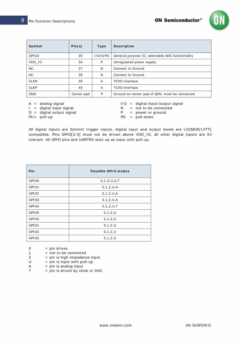
Symbol Pin(s) Type Description
GPIO3 35 I/O/A/PU General purpose IO, selectable ADC functionality
VDD_IO 36 P Unregulated power supply
NC 37 N Connect to Ground
NC 38 N Connect to Ground
CLKN 39 A TCXO interface
CLKP 40 A TCXO interface
GND Center pad P Ground on center pad of QFN, must be connected A = analog signal I/O = digital input/output signal I = digital input signal N = not to be connected O = digital output signal P = power or ground PU = pull-up PD = pull-down
All digital inputs are Schmitt trigger inputs, digital input and output levels are LVCMOS/LVTTL compatible. Pins GPIO[3:0] must not be driven above VDD_IO, all other digital inputs are 5V tolerant. All GPIO pins and UARTRX start up as input with pull-up.
Pin Possible GPIO modes
GPIO0 0,1,Z,U,A,T
GPIO1 0,1,Z,U,A
GPIO2 0,1,Z,U,A
GPIO3 0,1,Z,U,A
GPIO4 0,1,Z,U,T
GPIO5 0,1,Z,U
GPIO0 0,1,Z,U
GPIO1 0,1,Z,U
GPIO2 0,1,Z,U
GPIO3 0,1,Z,U
0 = pin drives 1 = not to be connected Z = pin is high impedance input U = pin is input with pull-up A = pin is analog input T = pin is driven by clock or DAC
Pin Function Descriptions
www.onsemi.com AX-SIGFOX/D
9
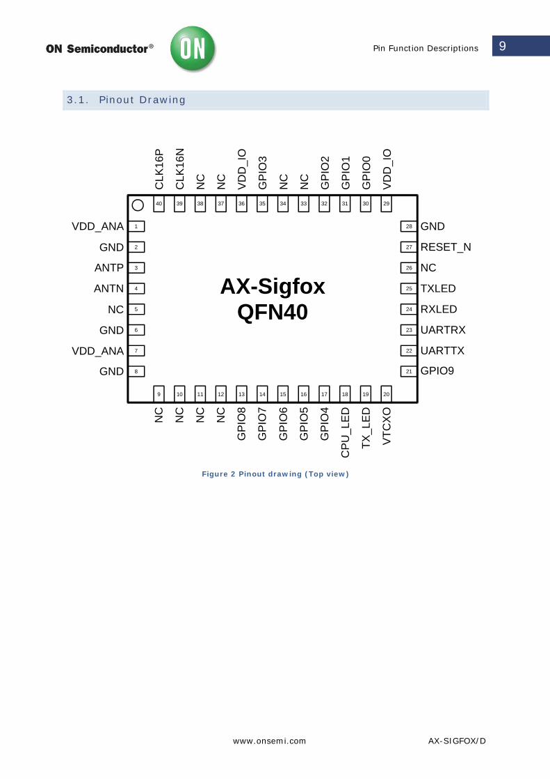
3.1. Pinout Drawing
GPIO9
AX-SigfoxQFN40
8
7
6
5
4
3
2
1
9 10 11 12 13 14 15 16 17 18 19 20
21
22
23
24
25
26
27
28
40 39 38 37 36 35 34 33 32 31 30 29
VDD_ANA
ANTP
GND
ANTN
NC
GND
GND
VDD_ANA
NC
NC
NC
NC
GP
IO8
GP
IO7
GP
IO6
GP
IO5
GP
IO4
TX_L
ED
VTC
XO
CLK
16P
CLK
16N
NC
NC
VD
D_I
O
GP
IO3
NC
NC
GP
IO2
GP
IO1
GP
IO0
VD
D_I
O
GND
RESET_N
NC
TXLED
RXLED
UARTRX
UARTTXC
PU
_LE
D
Figure 2 Pinout drawing (Top view)
Specifications
www.onsemi.com AX-SIGFOX/D
10
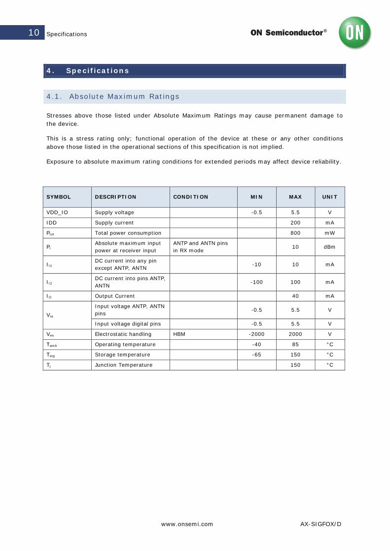
4. Specifications
4.1. Absolute Maximum Ratings
Stresses above those listed under Absolute Maximum Ratings may cause permanent damage to the device.
This is a stress rating only; functional operation of the device at these or any other conditions above those listed in the operational sections of this specification is not implied.
Exposure to absolute maximum rating conditions for extended periods may affect device reliability.
SYMBOL DESCRIPTION CONDITION MIN MAX UNIT
VDD_IO Supply voltage -0.5 5.5 V
IDD Supply current 200 mA
Ptot Total power consumption 800 mW
Pi Absolute maximum input power at receiver input
ANTP and ANTN pins in RX mode
10 dBm
II1 DC current into any pin except ANTP, ANTN
-10 10 mA
II2 DC current into pins ANTP, ANTN
-100 100 mA
IO Output Current 40 mA
Via Input voltage ANTP, ANTN pins
-0.5 5.5 V
Input voltage digital pins -0.5 5.5 V
Ves Electrostatic handling HBM -2000 2000 V
Tamb Operating temperature -40 85 °C
Tstg Storage temperature -65 150 °C
Tj Junction Temperature 150 °C
Specifications
www.onsemi.com AX-SIGFOX/D
11
4.2. DC Characteristics
Supplies
SYM DESCRIPTION CONDITION MIN TYP MAX UNIT
Conditions for all current and energy values unless otherwise specified are for the hardware configuration described in the AX-Sigfox Application Note: Sigfox Compliant Reference Design.
TAMB Operational ambient temperature -40 27 85 °C
VDDIO I/O and voltage regulator supply voltage
1.8 3.0 3.6 V
VDDIO_R1 I/O voltage ramp for reset activation; Note 1
Ramp starts at VDD_IO≤0.1V 0.1 V/ms
VDDIO_R2 I/O voltage ramp for reset activation; Note 1
Ramp starts at 0.1V<VDD_IO<0.7V 3.3 V/ms
IDS Deep sleep mode current AT$P=2 100 nA
ISLP Sleep mode current AT$P=1 1.3 μA
ISTDBY Standby mode current 0.5 mA
IRX_CONT Current consumption continuous RX AT$SR=1,1,-1 10 mA
QSFX_OOB_0 Energy to send a Sigfox out of band message, 0dBm
AT$S0 0.12 C
QSFX_BIT_0 Energy to send a bit, 0dBm AT$SB=0 0.08 C
QSFX_BITDL_0 Energy to send a bit with downlink receive, 0dBm
AT$SB=0,1 0.14 C
QSFX_LFR_0 Energy to send the longest possible Sigfox frame (12 byte) , 0dBm
AT$SF=00112233445566778899aabb 0.27 C
QSFX_LFRDL_0 Energy to send the longest possible Sigfox frame (12 byte) with downlink receive, 0dBm
AT$SF=00112233445566778899aabb,1 0.27 C
QSFX_OOB_14 Energy to send a Sigfox out of band message, 14dBm
AT$S0 0.28 C
QSFX_BIT_14 Energy to send a bit, 14dBm AT$SB=0 0.20 C
QSFX_BITDL_14 Energy to send a bit with downlink receive, 14dBm
AT$SB=0,1 0.35 C
QSFX_LFR_14 Energy to send the longest possible Sigfox frame (12 byte) , 14dBm
AT$SF=00112233445566778899aabb 0.39 C
QSFX_LFRDL_14 Energy to send the longest possible Sigfox frame (12 byte) with downlink receive, 14dBm
AT$SF=00112233445566778899aabb,1 0.46 C
ITXMOD0AVG Modulated Transmitter Current, Notes 3, 4
Pout=0 dBm; average 19.0 mA
ITXMOD14AVG Modulated Transmitter Current, Notes 3, 4
Pout=14 dBm; average 49.0 mA
Notes :
1. If VDD_IO ramps cannot be guaranteed, an external reset circuit is recommended, see the AX8052 Application Note: Power On Reset 2. Digital circuitry is functional down to typically 1 V. 3. The output power of the AX-Sigfox can be programmed in 1 dB steps from 0 dBm – 14 dBm. Current consumption values are given for a
matching network that is optimized for 14 dBm output. 0 dBm transmission with typically 10 mA can be achieved with other networks that are optimized for 0 dBm operation.
4. Values in dBm are typical, the matching network is optimized for 14 dBm
Specifications
www.onsemi.com AX-SIGFOX/D
12
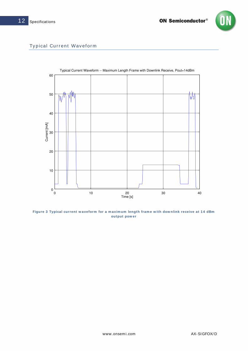
Typical Current Waveform
Figure 3 Typical current waveform for a maximum length frame with downlink receive at 14 dBm output power
Specifications
www.onsemi.com AX-SIGFOX/D
13
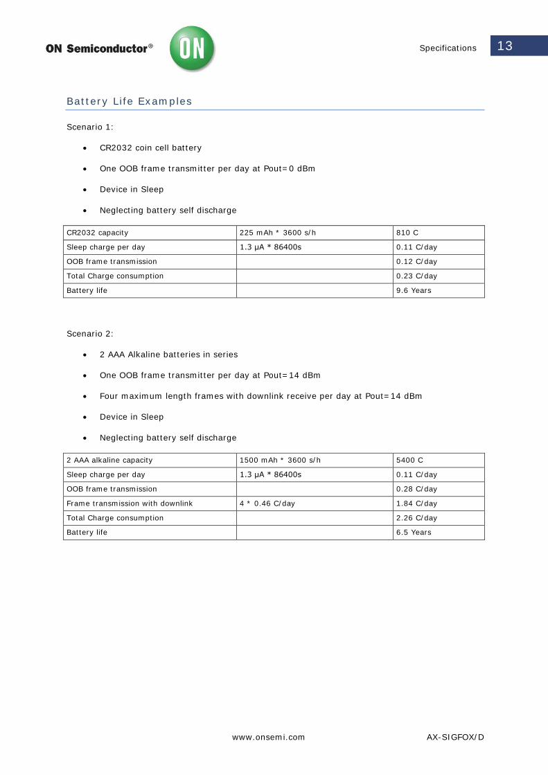
Battery Life Examples
Scenario 1:
• CR2032 coin cell battery
• One OOB frame transmitter per day at Pout=0 dBm
• Device in Sleep
• Neglecting battery self discharge
CR2032 capacity 225 mAh * 3600 s/h 810 C
Sleep charge per day 1.3 μA * 86400s 0.11 C/day
OOB frame transmission 0.12 C/day
Total Charge consumption 0.23 C/day
Battery life 9.6 Years
Scenario 2:
• 2 AAA Alkaline batteries in series
• One OOB frame transmitter per day at Pout=14 dBm
• Four maximum length frames with downlink receive per day at Pout=14 dBm
• Device in Sleep
• Neglecting battery self discharge
2 AAA alkaline capacity 1500 mAh * 3600 s/h 5400 C
Sleep charge per day 1.3 μA * 86400s 0.11 C/day
OOB frame transmission 0.28 C/day
Frame transmission with downlink 4 * 0.46 C/day 1.84 C/day
Total Charge consumption 2.26 C/day
Battery life 6.5 Years
Specifications
www.onsemi.com AX-SIGFOX/D
14
Logic
SYMBOL DESCRIPTION CONDITION MIN TYP MAX UNIT
DIGITAL INPUTS
VT+ Schmitt trigger low to high threshold point
VDD_IO = 3.3V
1.55 V
VT- Schmitt trigger high to low threshold point
1.25 V
VIL Input voltage, low 0.8 V
VIH Input voltage, high 2.0 V
VIPA Input voltage range, GPIO[3:0] -0.5 VDD_IO V
VIPBC Input voltage range, GPIO[9:4], UARTRX
-0.5 5.5 V
IL Input leakage current -10 10 μA
RPU Programmable Pull-Up Resistance
65 kΩ
DIGITAL OUTPUTS
IOH Output Current, high Ports GPIO[9:0], UARTTX, TXLED, RXLED, TXLED, CPULED
VOH= 2.4V 8 mA
IOL Output Current, low GPIO[9:0], UARTTX, TXLED, RXLED, TXLED, CPULED
VOL= 0.4V 8 mA
IOZ Tri-state output leakage current -10 10 μA
4.3. AC Characteristics
TCXO Reference Input
SYMBOL DESCRIPTION CONDITION MIN TYP MAX UNIT
fTCXO TCXO frequency
A passive network between the TCXO output and the pins CLKP and CLKN is required. For detailed TCXO network recommendations depending on the TCXO output swing refer to the AX5043 Application Note: Use with a TCXO Reference Clock. For TCXO recommendations see the Ax-Sigfox Application Note: Sigfox Compliant Reference Design
48 MHz
Specifications
www.onsemi.com AX-SIGFOX/D
15
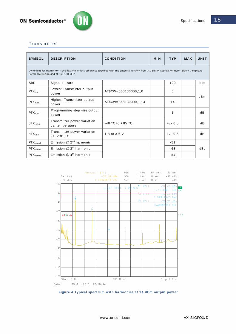
Transmitter
SYMBOL DESCRIPTION CONDITION MIN TYP MAX UNIT
Conditions for transmitter specifications unless otherwise specified with the antenna network from AX-Sigfox Application Note: Sigfox Compliant Reference Design and at 868.130 MHz.
SBR Signal bit rate 100 bps
PTXmin Lowest Transmitter output power
AT$CW=868130000,1,0 0 dBm
PTXmax Highest Transmitter output power
AT$CW=868130000,1,14 14
PTXstep Programming step size output power
1 dB
dTXtemp Transmitter power variation vs. temperature
-40 °C to +85 °C +/- 0.5 dB
dTXVdd Transmitter power variation vs. VDD_IO
1.8 to 3.6 V +/- 0.5 dB
PTXharm2 Emission @ 2nd harmonic
-51
dBc PTXharm3 Emission @ 3rd harmonic -63
PTXharm4 Emission @ 4th harmonic -84
Figure 4 Typical spectrum with harmonics at 14 dBm output power
Specifications
www.onsemi.com AX-SIGFOX/D
16
Receiver
SYM DESCRIPTION CONDITION MIN TYP MAX UNIT
Conditions for transmitter specifications unless otherwise specified with the antenna network from AX-Sigfox Application Note: Sigfox Compliant Reference Design and at 869.525 MHz.
SBR Signal bit rate 600 bps
ISBER868 AT$SB=x,1, AT$SF=x,1, AT$SR
PER < 0.1 -126 dBm
BLK868 Blocking at +/- 10MHz offset Channel/Blocker @ PER = 0.1, wanted signal level is +3 dB above the typical sensitivity, the blocker signal is CW
78 dB
ADC / Temperature Sensor
SYMBOL DESCRIPTION CONDITION MIN TYP MAX UNIT
ADCRES ADC resolution 10 Bits
VADCREF ADC reference voltage 0.95 1 1.05 V
ZADC00 Input capacitance 2.5 pF
DNL Differential nonlinearity +/- 1 LSB
INL Integral non inearity +/- 1 LSB
OFF Offset 3 LSB
GAIN_ERR Gain error 0.8 %
ADC in Differential Mode
VABS_DIFF Absolute voltages & common mode voltage in differential mode at each input
0 VDD_IO V
VFS_DIFF01 Full swing input for differential signals
Gain x1 -500 500 mV
VFS_DIFF10 Gain x10 -50 50 mV
ADC in Single Ended Mode
VMID_SE Mid code input voltage in single ended mode
0.5 V
VIN_SE00 Input voltage in single ended mode 0 VDD_IO V
VFS_SE01 Full swing input for single ended signals
Gain x1 0 1 V
Temperature Sensor
TRNG Temperature range AT$T? -40 85 °C
TERR_CAL Temperature error AT$T? -2 +2 °C
Command Interface
www.onsemi.com AX-SIGFOX/D
17
5. Command Interface
5.1. Serial Parameters: 9600,8,N,1
The AX-Sigfox uses the UART (pins UARTTX, UARTRX) to communicate with a host and uses a bitrate of 9600 baud, no parity, 8 data bits and one stop bit.
5.2. Power Modes
Standby
After Power-Up and after finishing a SIGFOX transmission, AX-Sigfox enters Standby mode. In Standby mode, AX-Sigfox listens on the UART for commands from the host. Also, OOB frames are transmitted whenever the OOB timer fires. To conserve power, the AX-Sigfox can be put into Sleep or turned off (Deep Sleep) completely.
Sleep
The command AT$P=1 is used to put the AX-Sigfox into Sleep mode. In this mode, only the wakeup timer for out-of-band messages is still running. To wake the AX-Sigfox up from Sleep mode toggle the serial UARTRX pin, e.g. by sending a break (break is an RS232 framing violation, i.e. at least 10 bit durations low). When an Out of Band (OOB) message is due, AX-Sigfox automatically wakes up to transmit the message, and then returns to Sleep mode.
Deep Sleep
In Deep Sleep mode, the AX-Sigfox is completely turned off and only draws negligible leakage current. Deep Sleep mode can be activated with AT$P=2. To wake-up from Deep Sleep mode, GPIO9 is pulled to GND.
Command Interface
www.onsemi.com AX-SIGFOX/D
18
When using Deep Sleep mode, keep two things in mind: Everything is turned off, timers are not running at all and all settings will be lost (use AT$WR to save settings to flash before entering Deep Sleep mode). Out-of-band messages will therefore not be sent. The pins states are frozen in Deep Sleep mode. The user must ensure that this will not result in condition which would draw a lot of current.
5.3. AT Commands
Numerical Syntax
hexdigit ::= [0-9A-Fa-f] hexnum ::= “0x” hexdigit+ decnum ::= “0” | [1-9] [0-9]* octnum ::= “0” [0-7]+ binnum ::= “0b” [01]+ bit ::= [01] optnum ::= “-1” frame ::= (hexdigit hexdigit)+ uint ::= hexnum | decnum | octnum | binnum uint_opt ::= uint | optnum
Command Syntax
A command starts with ‘AT’ (everything is case sensitive!), continues with the actual command followed by parameters (if any) and ends with any kind of whitespace (space, tab, newline etc.)
If incorrect syntax is detected (“parsing error”) all input is ignored up until the next whitespace character.
Also note that any number can be entered in any format (Hexadecimal, Decimal, Octal and binary) by adding the corresponding prefix (‘0x’, ‘0’, ‘0b’). The only exception is the 'Send Frame' command (AT$SF) which expects a list of hexadecimal digits without any prefix.
Return Codes
A successful command execution is indicated by sending ‘OK’. If a command returns a value (e.g. by querying a register) only the value is returned.
Examples
Bold text is sent to AX-Sigfox.
AT$I=0 AXSEM AT Command Interface
Here, we execute command ‘I’ to query some general information.
AT$SF=aabb1234 OK
Command Interface
www.onsemi.com AX-SIGFOX/D
19
This sends a Sigfox frame containing 0x00 : 0x11 : 0x22 : 0x33 : 0x44 , then waits for a downlink response telegram, which in this example contains 0xAA : 0xBB : 0xCC : 0xDD .
AT$SF=0011223344,1 OK RX=AA BB CC DD
This sends a Sigfox frame containing 0xAA : 0xBB : 0x12 : 0x34 without waiting for a response telegram.
AT$CB=0xAA,1 OK
The ‘CB’ command sends out a continuous pattern of bits, in this case 0xAA = 0b10101010.
AT$P=1 OK
This transitions the device into sleep mode. Out-of-band transmissions will still be triggered. The UART is powered down. The device can be woken up by a low level on the UART signal, i.e. by sending break.
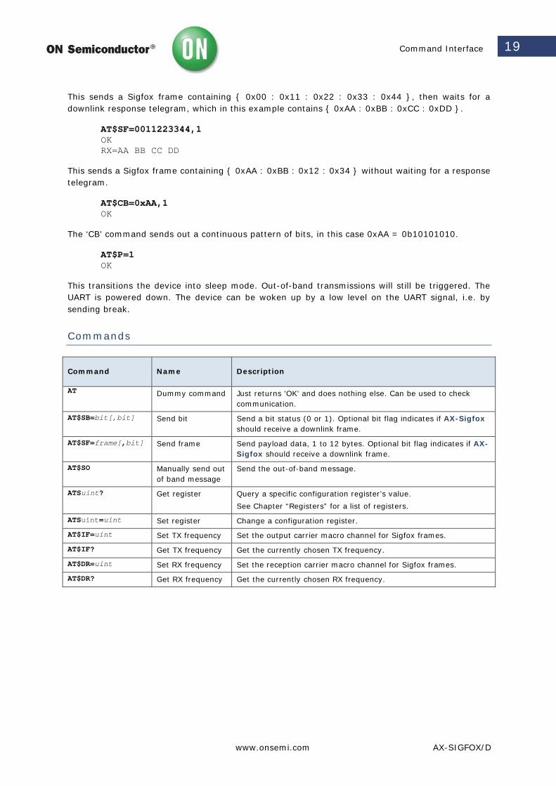
Commands
Command Name Description
AT Dummy command Just returns 'OK' and does nothing else. Can be used to check communication.
AT$SB=bit[,bit] Send bit Send a bit status (0 or 1). Optional bit flag indicates if AX-Sigfox should receive a downlink frame.
AT$SF=frame[,bit] Send frame Send payload data, 1 to 12 bytes. Optional bit flag indicates if AX-Sigfox should receive a downlink frame.
AT$SO Manually send out of band message
Send the out-of-band message.
ATSuint? Get register Query a specific configuration register’s value. See Chapter “Registers” for a list of registers.
ATSuint=uint Set register Change a configuration register.
AT$IF=uint Set TX frequency Set the output carrier macro channel for Sigfox frames.
AT$IF? Get TX frequency Get the currently chosen TX frequency.
AT$DR=uint Set RX frequency Set the reception carrier macro channel for Sigfox frames.
AT$DR? Get RX frequency Get the currently chosen RX frequency.
Command Interface
www.onsemi.com AX-SIGFOX/D
20
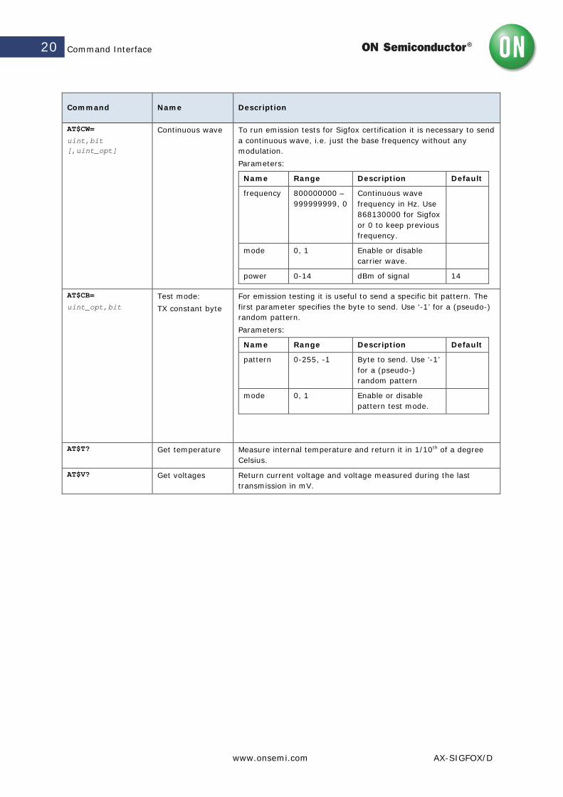
Command Name Description
AT$CW= uint,bit [,uint_opt]
Continuous wave To run emission tests for Sigfox certification it is necessary to send a continuous wave, i.e. just the base frequency without any modulation. Parameters:
Name Range Description Default
frequency 800000000 – 999999999, 0
Continuous wave frequency in Hz. Use 868130000 for Sigfox or 0 to keep previous frequency.
mode 0, 1 Enable or disable carrier wave.
power 0-14 dBm of signal 14
AT$CB= uint_opt,bit
Test mode: TX constant byte
For emission testing it is useful to send a specific bit pattern. The first parameter specifies the byte to send. Use ‘-1’ for a (pseudo-) random pattern. Parameters:
Name Range Description Default
pattern 0-255, -1 Byte to send. Use ‘-1’ for a (pseudo-) random pattern
mode 0, 1 Enable or disable pattern test mode.
AT$T? Get temperature Measure internal temperature and return it in 1/10th of a degree Celsius.
AT$V? Get voltages Return current voltage and voltage measured during the last transmission in mV.
Command Interface
www.onsemi.com AX-SIGFOX/D
21
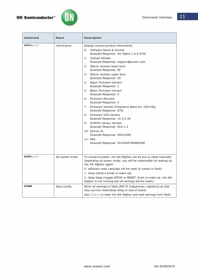
Command Name Description
AT$I=uint Information Display various product information: 0: Software Name & Version
Example Response: AX-Sigfox 1.0.6-ETSI 1: Contact Details
Example Response: [email protected] 2: Silicon revision lower byte
Example Response: 8F 3: Silicon revision upper byte
Example Response: 00 4: Major Firmware Version
Example Response: 1 5: Minor Firmware Version
Example Response: 0 6: Firmware Revision
Example Response: 3 7: Firmware Variant (Frequency Band etc. (EU/US))
Example Response: ETSI 8: Firmware VCS Version
Example Response: v1.0.2-36 9: SIGFOX Library Version
Example Response: DL0-1.4 10: Device ID
Example Response: 00012345 11: PAC
Example Response: 0123456789ABCDEF
AT$P=uint Set power mode To conserve power, the AX-Sigfox can be put to sleep manually. Depending on power mode, you will be responsible for waking up the AX-Sigfox again! 0: software reset (settings will be reset to values in flash) 1: sleep (send a break to wake up) 2: deep sleep (toggle GPIO9 or RESET_N pin to wake up; the AX-Sigfox is not running and all settings will be reset!)
AT$WR Save config Write all settings to flash (RX/TX frequencies, registers) so that they survive reset/deep sleep or loss of power. Use AT$P=0 to reset the AX-Sigfox and load settings from flash.
Command Interface
www.onsemi.com AX-SIGFOX/D
22
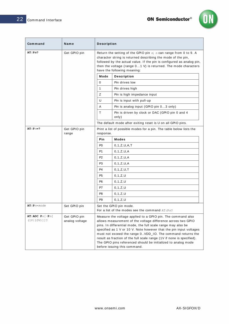
Command Name Description
AT:Pn? Get GPIO pin Return the setting of the GPIO pin n; n can range from 0 to 9. A character string is returned describing the mode of the pin, followed by the actual value. If the pin is configured as analog pin, then the voltage (range 0...1 V) is returned. The mode characters have the following meaning:
Mode Description
0 Pin drives low
1 Pin drives high
Z Pin is high impedance input
U Pin is input with pull-up
A Pin is analog input (GPIO pin 0...3 only)
T Pin is driven by clock or DAC (GPIO pin 0 and 4 only)
The default mode after exiting reset is U on all GPIO pins.
AT:Pn=? Get GPIO pin range
Print a list of possible modes for a pin. The table below lists the response.
Pin Modes
P0 0,1,Z,U,A,T
P1 0,1,Z,U,A
P2 0,1,Z,U,A
P3 0,1,Z,U,A
P4 0,1,Z,U,T
P5 0,1,Z,U
P6 0,1,Z,U
P7 0,1,Z,U
P8 0,1,Z,U
P9 0,1,Z,U
AT:Pn=mode Set GPIO pin Set the GPIO pin mode. For a list of the modes see the command AT:Pn?
AT:ADC Pn[-Pn[ (1V|10V)]]?
Get GPIO pin analog voltage
Measure the voltage applied to a GPIO pin. The command also allows measurement of the voltage difference across two GPIO pins. In differential mode, the full scale range may also be specified as 1 V or 10 V. Note however that the pin input voltages must not exceed the range 0..VDD_IO. The command returns the result as fraction of the full scale range (1V if none is specified). The GPIO pins referenced should be initialized to analog mode before issuing this command.
Command Interface
www.onsemi.com AX-SIGFOX/D
23
Command Name Description
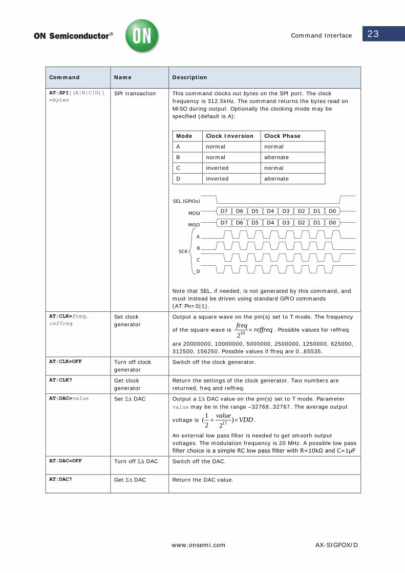
AT:SPI[(A|B|C|D)]=bytes
SPI transaction This command clocks out bytes on the SPI port. The clock frequency is 312.5kHz. The command returns the bytes read on MISO during output. Optionally the clocking mode may be specified (default is A):
Mode Clock Inversion Clock Phase
A normal normal
B normal alternate
C inverted normal
D inverted alternate
Note that SEL, if needed, is not generated by this command, and must instead be driven using standard GPIO commands (AT:Pn=0|1).
AT:CLK=freq, reffreq
Set clock generator
Output a square wave on the pin(s) set to T mode. The frequency
of the square wave is reffreqfreq×162
. Possible values for reffreq
are 20000000, 10000000, 5000000, 2500000, 1250000, 625000, 312500, 156250. Possible values if ffreq are 0…65535.
AT:CLK=OFF Turn off clock generator
Switch off the clock generator.
AT:CLK? Get clock generator
Return the settings of the clock generator. Two numbers are returned, freq and reffreq.
AT:DAC=value Set Σ∆ DAC Output a Σ∆ DAC value on the pin(s) set to T mode. Parameter value may be in the range –32768..32767. The average output
voltage is VDDvalue×+ )
221( 17 .
An external low pass filter is needed to get smooth output voltages. The modulation frequency is 20 MHz. A possible low pass filter choice is a simple RC low pass filter with R=10kΩ and C=1μF
AT:DAC=OFF Turn off Σ∆ DAC Switch off the DAC.
AT:DAC? Get Σ∆ DAC Return the DAC value.
Command Interface
www.onsemi.com AX-SIGFOX/D
24
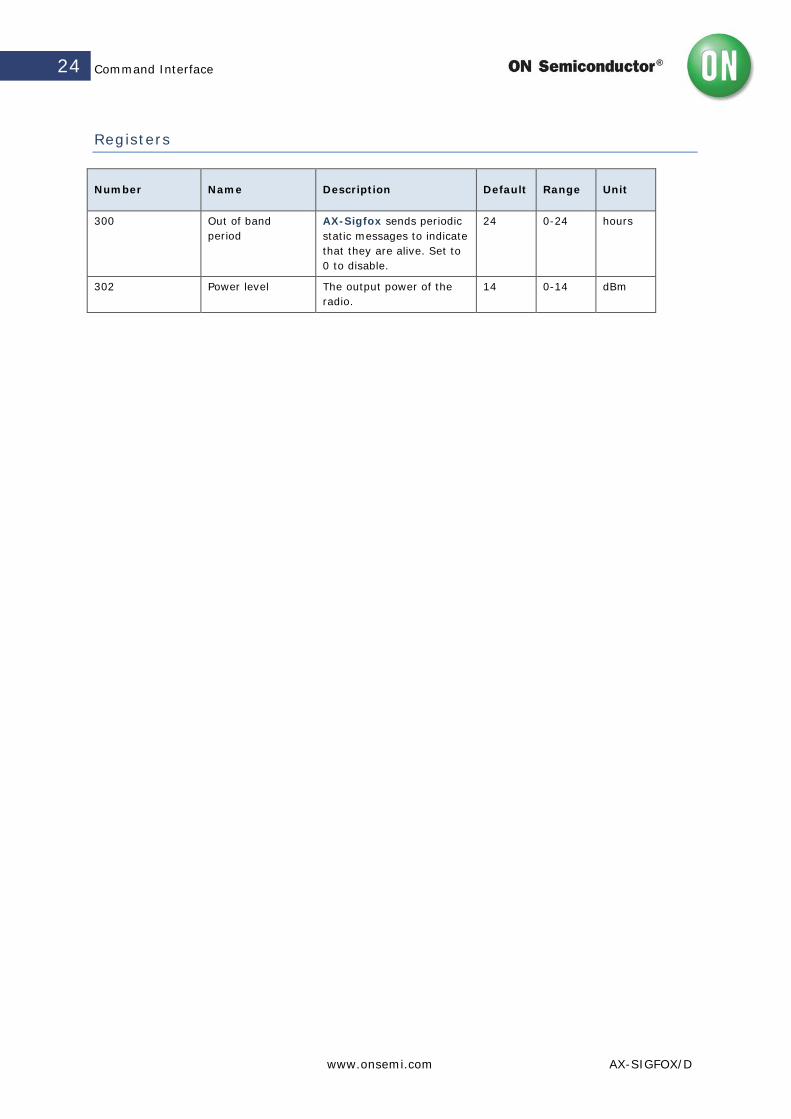
Registers
Number Name Description Default Range Unit
300 Out of band period
AX-Sigfox sends periodic static messages to indicate that they are alive. Set to 0 to disable.
24 0-24 hours
302 Power level The output power of the radio.
14 0-14 dBm
Application Information
www.onsemi.com AX-SIGFOX/D
25
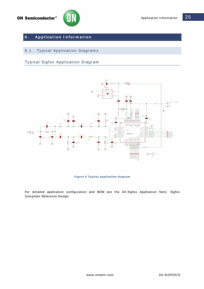
6. Application Information
6.1. Typical Application Diagrams
Typical Sigfox Application Diagram
Figure 5 Typical application diagram
For detailed application configuration and BOM see the AX-Sigfox Application Note: Sigfox Compliant Reference Design.
QFN40 Package Information
www.onsemi.com AX-SIGFOX/D
26
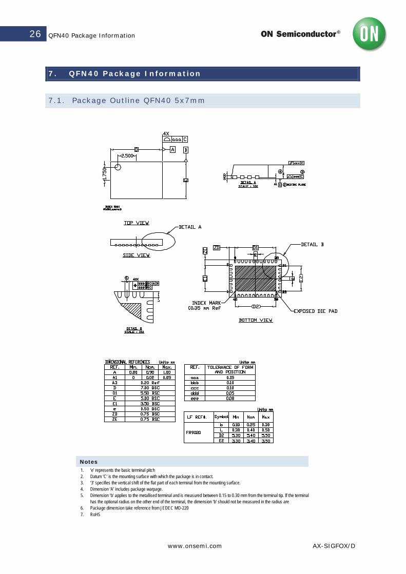
7. QFN40 Package Information
7.1. Package Outline QFN40 5x7mm
Notes 1. ‘e’ represents the basic terminal pitch 2. Datum ‘C’ is the mounting surface with which the package is in contact. 3. ‘3’ specifies the vertical shift of the flat part of each terminal from the mounting surface. 4. Dimension ‘A’ includes package warpage. 5. Dimension ‘b’ applies to the metallised terminal and is measured between 0.15 to 0.30 mm from the terminal tip. If the terminal
has the optional radius on the other end of the terminal, the dimension ‘b’ should not be measured in the radius are 6. Package dimension take reference from JEDEC MO-220 7. RoHS
QFN40 Package Information
www.onsemi.com AX-SIGFOX/D
27
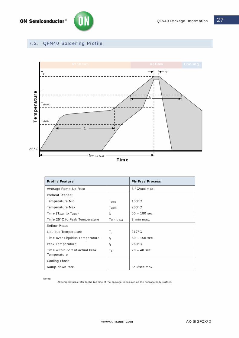
7.2. QFN40 Soldering Profile
Profile Feature Pb-Free Process
Average Ramp-Up Rate 3 °C/sec max.
Preheat Preheat
Temperature Min TsMIN 150°C
Temperature Max TsMAX 200°C
Time (TsMIN to TsMAX) ts 60 – 180 sec
Time 25°C to Peak Temperature T25 ° to Peak 8 min max.
Reflow Phase
Liquidus Temperature TL 217°C
Time over Liquidus Temperature tL 60 – 150 sec
Peak Temperature tp 260°C
Time within 5°C of actual Peak Temperature
Tp 20 – 40 sec
Cooling Phase
Ramp-down rate 6°C/sec max.
Notes: All temperatures refer to the top side of the package, measured on the package body surface.
Time
Tp
TL
TsMAX
TsMIN
t25° to Peak
ts
tL
25°C
Preheat Reflow Cooling
tp
Tem
per
atu
re
QFN40 Package Information
www.onsemi.com AX-SIGFOX/D
28
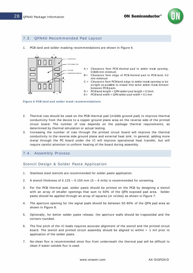
7.3. QFN40 Recommended Pad Layout
1. PCB land and solder masking recommendations are shown in Figure 6.
A = Clearance from PCB thermal pad to solder mask opening, 0.0635 mm minimum
B = Clearance from edge of PCB thermal pad to PCB land, 0.2 mm minimum
C = Clearance from PCB land edge to solder mask opening to be as tight as possible to ensure that some solder mask remains between PCB pads
D = PCB land length = QFN solder pad length + 0.1mm E = PCB land width = QFN solder pad width + 0.1 mm
Figure 6 PCB land and solder mask recommendations
2. Thermal vias should be used on the PCB thermal pad (middle ground pad) to improve thermal conductivity from the device to a copper ground plane area on the reverse side of the printed circuit board. The number of vias depends on the package thermal requirements, as determined by thermal simulation or actual testing.
3. Increasing the number of vias through the printed circuit board will improve the thermal conductivity to the reverse side ground plane and external heat sink. In general, adding more metal through the PC board under the IC will improve operational heat transfer, but will require careful attention to uniform heating of the board during assembly.
7.4. Assembly Process
Stencil Design & Solder Paste Application
1. Stainless steel stencils are recommended for solder paste application.
2. A stencil thickness of 0.125 – 0.150 mm (5 – 6 mils) is recommended for screening.
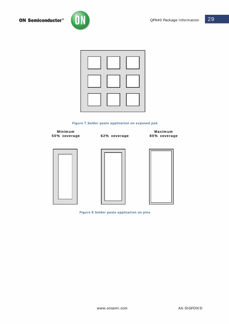
3. For the PCB thermal pad, solder paste should be printed on the PCB by designing a stencil with an array of smaller openings that sum to 50% of the QFN exposed pad area. Solder paste should be applied through an array of squares (or circles) as shown in Figure 7.
4. The aperture opening for the signal pads should be between 50-80% of the QFN pad area as shown in Figure 8.
5. Optionally, for better solder paste release, the aperture walls should be trapezoidal and the corners rounded.
6. The fine pitch of the IC leads requires accurate alignment of the stencil and the printed circuit board. The stencil and printed circuit assembly should be aligned to within + 1 mil prior to application of the solder paste.
7. No-clean flux is recommended since flux from underneath the thermal pad will be difficult to clean if water-soluble flux is used.
QFN40 Package Information
www.onsemi.com AX-SIGFOX/D
29
Figure 7 Solder paste application on exposed pad
Minimum 50% coverage
62% coverage
Maximum 80% coverage
Figure 8 Solder paste application on pins
Device Versions
www.onsemi.com AX-SIGFOX/D
30
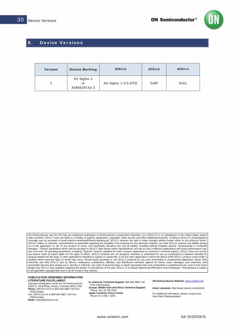
8. Device Versions
Version Device Marking AT$I=0 AT$I=2 AT$I=3
1 AX-Sigfox-1
or AX8052F143-2
AX-Sigfox 1.0.6-ETSI 0x8F 0x51
ON Semiconductor and the ON logo are registered trademarks of Semiconductor Components Industries, LLC (SCILLC) or its subsidiaries in the United States and/or other countries. SCILLC owns the rights to a number of patents, trademarks, copyrights, trade secrets, and other intellectual property. A listing of SCILLC’s product/patent coverage may be accessed at www.onsemi.com/site/pdf/Patent-Marking.pdf. SCILLC reserves the right to make changes without further notice to any products herein. SCILLC makes no warranty, representation or guarantee regarding the suitability of its products for any particular purpose, nor does SCILLC assume any liability arising out of the application or use of any product or circuit, and specifically disclaims any and all liability, including without limitation special, consequential or incidental damages. “Typical” parameters which may be provided in SCILLC data sheets and/or specifications can and do vary in different applications and actual performance may vary over time. All operating parameters, including “Typicals” must be validated for each customer application by customer’s technical experts. SCILLC does not convey any license under its patent rights nor the rights of others. SCILLC products are not designed, intended, or authorized for use as components in systems intended for surgical implant into the body, or other applications intended to support or sustain life, or for any other application in which the failure of the SCILLC product could create a situation where personal injury or death may occur. Should Buyer purchase or use SCILLC products for any such unintended or unauthorized application, Buyer shall indemnify and hold SCILLC and its officers, employees, subsidiaries, affiliates, and distributors harmless against all claims, costs, damages, and expenses, and reasonable attorney fees arising out of, directly or indirectly, any claim of personal injury or death associated with such unintended or unauthorized use, even if such claim alleges that SCILLC was negligent regarding the design or manufacture of the part. SCILLC is an Equal Opportunity/Affirmative Action Employer. This literature is subject to all applicable copyright laws and is not for resale in any manner. PUBLICATION ORDERING INFORMATION LITERATURE FULFILLMENT: Literature Distribution Center for ON Semiconductor 19521 E. 32nd Pkwy, Aurora, Colorado 80011 USA Phone: 303-675-2175 or 800-344-3860 Toll Free
USA/Canada Fax: 303-675-2176 or 800-344-3867 Toll Free
USA/Canada Email: [email protected]
N. American Technical Support: 800-282-9855 Toll Free USA/Canada. Europe, Middle East and Africa Technical Support:
Phone: 421 33 790 2910 Japan Customer Focus Center Phone: 81-3-5817-1050
ON Semiconductor Website: www.onsemi.com
Order Literature: http://www.onsemi.com/orderlit For additional information, please contact your local Sales Representative