ax5051-51052ebad10ee97eea25d5e-d7d40819259e7d3022d9ad53e3694148.r84.cf3.rackcdn… · datasheet...
TRANSCRIPT

DATASHEET
AX5051-510
470-510 MHz ASK/FSK/PSK Transceiver
Datasheet extension for AX5051
Version 1.13-510

Version 1.13-510 Datasheet AX5051-510
2
Document Type Datasheet
Document Status
Document Version Version 1.13-510
Product AX5051-510

Table of Contents 3
Table of Contents
1. Overview..................................................................................................... 4
1.1. Features ..................................................................................................... 4
1.2. Applications................................................................................................. 4
2. Block Diagram............................................................................................. 5
3. Pin Function Descriptions ........................................................................... 6
3.1. Pin-out Drawing ........................................................................................... 7
4. Specifications.............................................................................................. 8
4.1. Absolute Maximum Ratings ............................................................................ 8
4.2. DC Characteristics ........................................................................................ 9
Supplies ...................................................................................................... 9
Logic......................................................................................................... 10
4.3. AC Characteristics ...................................................................................... 11
Crystal Oscillator ........................................................................................ 11
RF Frequency Generation Subsystem (Synthesizer) ......................................... 12
Transmitter................................................................................................ 13
Receiver .................................................................................................... 13
SPI Timing................................................................................................. 15
5. Life Support Applications .......................................................................... 16
6. Contact Information.................................................................................. 17
Version 1.13-510 Datasheet AX5051-510

Overview 4
1. Overview
This datasheet explains the parameters of AX5051 in the Chinese ISM bands between 470-510 MHz. The specification between 400-470 MHz and 800-940 MHz stays unchanged.
1.1. Features
• Configurable for usage between 470 and 510 MHz
1.2. Applications
Operation in the Chinese ISM bands between 470 MHz and 510 MHz.
• Telemetry
• Sensor readout, thermostats
• AMR
• Toys
• Wireless audio
• Wireless networks
• Wireless M-Bus
• Access control
• Remote keyless entry
• Remote controls
• Active RFID
Version 1.13-510 Datasheet AX5051-510

Block Diagram 5
2. Block Diagram
Figure 1 Functional block diagram of the AX5051
AX5051
4ANTP
5ANTN
IF Filter & AGC PGAs
AGC
Crystal Oscillator
typ. 16 MHz
FOUT
RF Frequency Generation Subsystem
FXTAL
Communication Controller & Serial Interface
Divider
ADC
Mixer Digital IF channel
filter
LN
PA
De- modulator
Enco
der
Fram
ing
FIFO
Modulator
13
SYSC
LK
27
CLK16P
28
CLK16N
RSS
Chip configuration
12
RESET_N
19
IRQ
16 15 14 SEL
CLK
MISO
17
MOSI
24
VREG
VDD_IO
20
Voltage Regulator POR
Version 1.13-510 Datasheet AX5051-510
Pin Function Descriptions 6
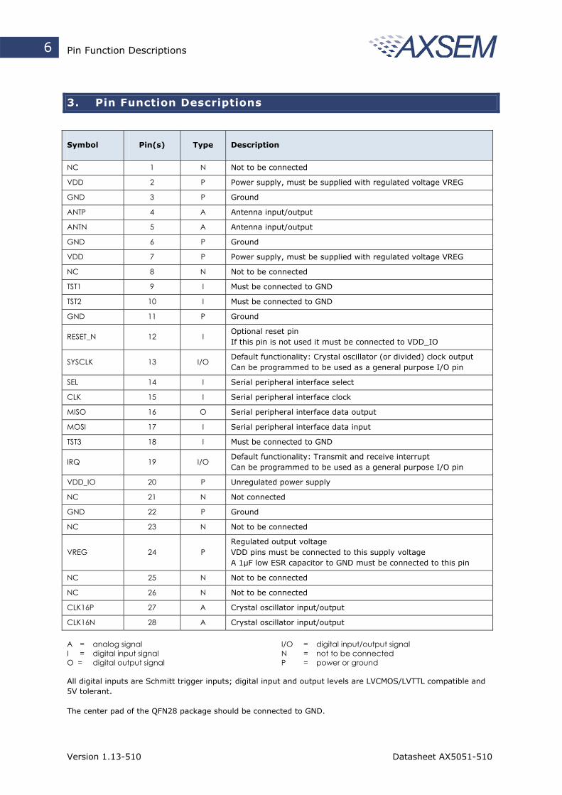
3. Pin Function Descriptions
Symbol Pin(s) Type Description
NC 1 N Not to be connected
VDD 2 P Power supply, must be supplied with regulated voltage VREG
GND 3 P Ground
ANTP 4 A Antenna input/output
ANTN 5 A Antenna input/output
GND 6 P Ground
VDD 7 P Power supply, must be supplied with regulated voltage VREG
NC 8 N Not to be connected
TST1 9 I Must be connected to GND
TST2 10 I Must be connected to GND
GND 11 P Ground
RESET_N 12 IOptional reset pin If this pin is not used it must be connected to VDD_IO
SYSCLK 13 I/ODefault functionality: Crystal oscillator (or divided) clock output Can be programmed to be used as a general purpose I/O pin
SEL 14 I Serial peripheral interface select
CLK 15 I Serial peripheral interface clock
MISO 16 O Serial peripheral interface data output
MOSI 17 I Serial peripheral interface data input
TST3 18 I Must be connected to GND
IRQ 19 I/ODefault functionality: Transmit and receive interrupt Can be programmed to be used as a general purpose I/O pin
VDD_IO 20 P Unregulated power supply
NC 21 N Not connected
GND 22 P Ground
NC 23 N Not to be connected
VREG 24 PRegulated output voltage VDD pins must be connected to this supply voltage A 1µF low ESR capacitor to GND must be connected to this pin
NC 25 N Not to be connected
NC 26 N Not to be connected
CLK16P 27 A Crystal oscillator input/output
CLK16N 28 A Crystal oscillator input/output
A = analog signal I/O = digital input/output signal I = digital input signal N = not to be connected O = digital output signal P = power or ground All digital inputs are Schmitt trigger inputs; digital input and output levels are LVCMOS/LVTTL compatible and 5V tolerant. The center pad of the QFN28 package should be connected to GND.
Version 1.13-510 Datasheet AX5051-510

Pin Function Descriptions 7
3.1. Pin-out Drawing
CLK
16N
Figure 2: Pin-out drawing (Top vi
222325 24262728CLK
16P
VREG
GN
D
NC
NC
NC
AX5051
16
17
18
19
20
21
15
6
5
4
3
2
1
7
NC NC
VDD_IO VDD
I GND
T ANTP
MOSI ANTN
M GND
CVDD
8 9 10 1211 13 14
SYSCL
GN
D
RESET
N
TST1
TST2
SEL
NC
Version 1.13-510
ISO
ST3
RQ
ew)
LK
Datasheet AX5051-510
Specifications 8
4. Specifications
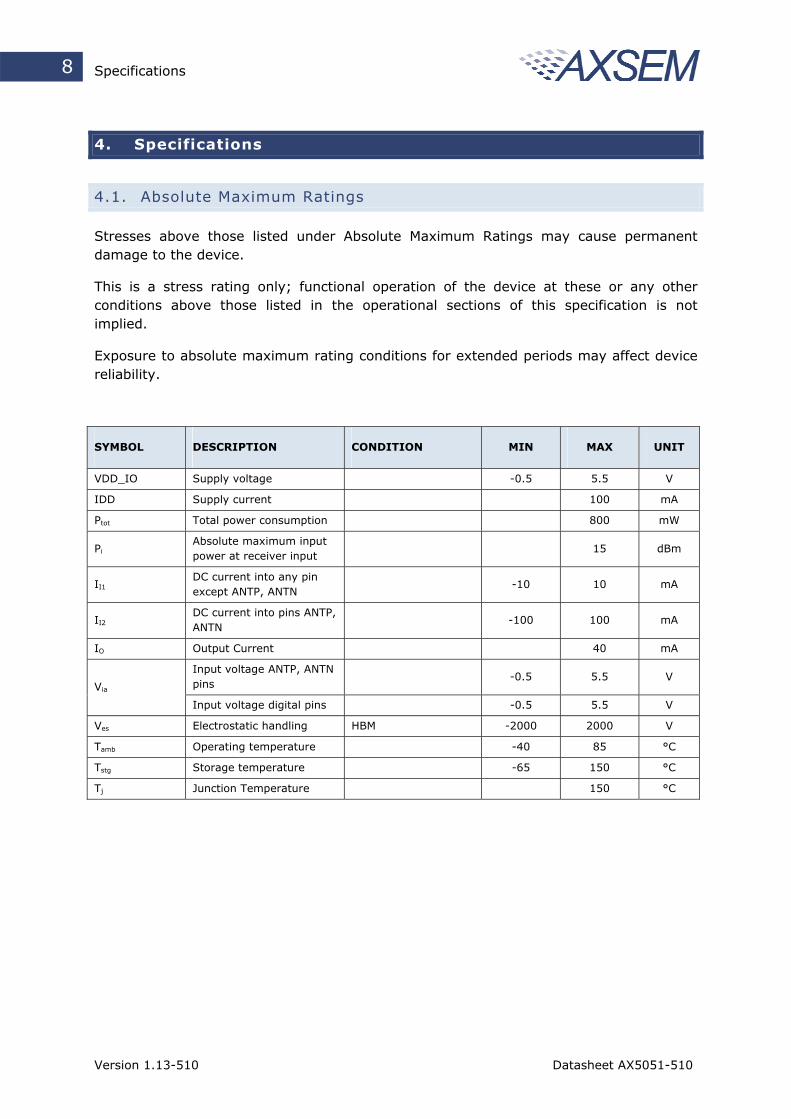
4.1. Absolute Maximum Ratings
Stresses above those listed under Absolute Maximum Ratings may cause permanent damage to the device.
This is a stress rating only; functional operation of the device at these or any other conditions above those listed in the operational sections of this specification is not implied.
Exposure to absolute maximum rating conditions for extended periods may affect device reliability.
SYMBOL DESCRIPTION CONDITION MIN MAX UNIT
VDD_IO Supply voltage -0.5 5.5 V
IDD Supply current 100 mA
Ptot Total power consumption 800 mW
PiAbsolute maximum input power at receiver input
15 dBm
II1DC current into any pin except ANTP, ANTN
-10 10 mA
II2DC current into pins ANTP, ANTN
-100 100 mA
IO Output Current 40 mA
Input voltage ANTP, ANTN pins
-0.5 5.5 V Via
Input voltage digital pins -0.5 5.5 V
Ves Electrostatic handling HBM -2000 2000 V
Tamb Operating temperature -40 85 °C
Tstg Storage temperature -65 150 °C
Tj Junction Temperature 150 °C
Version 1.13-510 Datasheet AX5051-510

Specifications 9
4.2. DC Characteristics
Supplies
SYMBOL DESCRIPTION CONDITION MIN TYP MAX UNIT
TAMBOperational ambient temperature
-40 27 85 °C
RX operation or TX operation up to 4 dBm output power
2.4 3.0 3.6 V
VDD_IO I/O and voltage regulator supply voltage
TX operation up to 12 dBm output power
2.5 3.0 3.6 V
Power-down mode PWRMODE=0x00
1.7 V VREG
Internally regulated supply voltage
All other power modes 2.1 2.5 2.8 V
VREGdroptyp Regulator voltage drop RX operation or TX operation up to 4 dBm output power
50 mV
VREGdropmax
Regulator voltage drop at maximum internal current consumption
TX mode with 12 dBm output power
300 mV
IPDOWN Power-down current PWRMODE=0x00 0.5 µA
IRX-HS
Current consumption RX
High sensitivity mode: VCO_I=001; REF_I=011
Bit rate 10 kbit/s 19 mA
IRX-LP
Current consumption RX
Low power mode: VCO_I=001; REF_I=101
Bit rate 10 kbit/s 17 mA
470 MHz, 10 dBm 28
470 MHz, 0 dBm 19
470 MHz, 15 dBm 45 ITX
Current consumption TX
VCO_I=001; REF_I=011; LOCURST=1
470 MHz, min power 11
mA
Version 1.13-510 Datasheet AX5051-510

Specifications 10
Logic
SYMBOL DESCRIPTION CONDITION MIN. TYP. MAX. UNIT
DIGITAL INPUTS
VT+Schmitt trigger low to high threshold point
1.9 V
VT-Schmitt trigger high to low threshold point
1.2 V
VIL Input voltage, low 0.8 V
VIH Input voltage, high 2.0 V
IL Input leakage current -10 10 µA
DIGITAL OUTPUTS
IOH Output Current, high VOH= 2.4V 4 mA
IOL Output Current, low VOL= 0.4V 4 mA
IOZ Tri-state output leakage current -10 10 µA
Version 1.13-510 Datasheet AX5051-510

Specifications 11
4.3. AC Characteristics
Crystal Oscillator
SYMBOL DESCRIPTION CONDITION MIN. TYP. MAX. UNIT
fXTAL Crystal frequency Note 1, 3 15.5 16 25 MHz
XTALOSCGM=0000 1
XTALOSCGM=0001 2
XTALOSCGM =0010 default
3
XTALOSCGM =0011 4
XTALOSCGM =0100 5
XTALOSCGM =0101 6
XTALOSCGM =0110 6.5
XTALOSCGM =0111 7
XTALOSCGM =1000 7.5
XTALOSCGM =1001 8
XTALOSCGM =1010 8.5
XTALOSCGM =1011 9
XTALOSCGM =1100 9.5
XTALOSCGM =1101 10
XTALOSCGM =1110 10.5
gmosc Transconductance oscillator
XTALOSCGM =1111 11
mS
XTALCAP = 000000
default 2 pF
Cosc
Programmable tuning capacitors at pins CLK16N and CLK16P XTALCAP = 111111 33 pF
Cosc-lsb
Programmable tuning capacitors, increment per LSB of XTALCAP
0.5 pF
fext External clock input Note 2, 3 15.5 16 25 MHz
RINosc Input DC impedance 10 kΩ Notes
1. Tolerances and start-up times depend on the crystal used. Depending on the RF frequency and channel spacing the IC must be calibrated to the exact crystal frequency using the readings of the register TRKFREQ
2. If an external clock is used, it should be input via an AC coupling at pin CLK16P with the oscillator powered up and XTALCAP=000000 3. Lower frequencies than 15.5 MHz or higher frequencies than 25 MHz can be used. However not all typical RF frequencies can than be
generated
Version 1.13-510 Datasheet AX5051-510

Specifications 12
RF Frequency Generation Subsystem (Synthesizer)
SYMBOL DESCRIPTION CONDITION MIN TYP MAX UNIT
fREF Reference frequency Note 1 16
24 MHz
frange_hi BANDSEL=0
frange_low
Frequency range BANDSEL=1 470 510
MHz
fRESO Frequency resolution 1 Hz
BW1
Loop filter configuration: FLT=01 Charge pump current: PLLCPI=010
100
BW2
Loop filter configuration: FLT=01 Charge pump current: PLLCPI=001
50
BW3
Loop filter configuration: FLT=11
Charge pump current: PLLCPI=010
200
BW4
Synthesizer loop bandwidth
VCO current: VCOI=001
Loop filter configuration: FLT=10 Charge pump current: PLLCPI=010
500
kHz
Tset1
Loop filter configuration: FLT=01 Charge pump current: PLLCPI=010
15
Tset2
Loop filter configuration: FLT=01 Charge pump current: PLLCPI=001
30
Tset3
Loop filter configuration: FLT=11 Charge pump current: PLLCPI=010
7
Tset4
Synthesizer settling time for 1MHz step as typically required for RX/TX switching
VCO current: VCO_I=001
Loop filter configuration: FLT=10 Charge pump current: PLLCPI=010
3
µs
Tstart1
Loop filter configuration: FLT=01 Charge pump current: PLLCPI=010
25
Tstart2
Loop filter configuration: FLT=01 Charge pump current: PLLCPI=001
50
Tstart3
Loop filter configuration: FLT=11 Charge pump current: PLLCPI=010
12
Tstart4
Synthesizer start-up time if crystal oscillator and reference are running
VCO current: VCO_I=001
Loop filter configuration: FLT=10 Charge pump current: PLLCPI=010
5
µs
470 MHz, 50 kHz from carrier -90
470 MHz, 100 kHz from carrier -95
470 MHz, 300 kHz from carrier -105 PN470
Synthesizer phase noise Loop filter configuration: FLT=01 Charge pump current: PLLCPI=010 VCO current: VCO_I=001 470 MHz, 2 MHz from carrier -115
dBc/Hz
Notes 1. ASK, PSK and 0.1-200 kbps FSK with 16 MHz crystal, 200-350 kbps FSK with 24 MHz crystal
Version 1.13-510 Datasheet AX5051-510

Specifications 13
Transmitter
SYMBOL DESCRIPTION CONDITION MIN. TYP. MAX. UNIT
ASK 1 600
PSK 10 600 SBR Signal bit rate
FSK 1 350
kbps
PTX470
Transmitter power
@ 470 MHz
TXRNG=1111
LOCURST=1 15 dBm
Notes Note 1. 1-200 kbps with a 16 MHz crystal, 200-350 kbps with a 24 MHz crystal
Receiver
Datarate Input sensitivity TYP. on SMA connector for BER=10-3
kbps ASK FSK h=1 FSK h=4 FSK h=8 FSK h=16 PSK
1.2 -115 -116
2 -115 -115
10 -103 -109 -110
100 -97 -103 -98 -104
200 -94 -100 -100
600 -90 -98
Condition: 470 MHz
Version 1.13-510 Datasheet AX5051-510

Specifications 14
SYMBOL DESCRIPTION CONDITION MIN. TYP. MAX. UNIT
ASK 1 600
PSK 10 600
FSK 1 350 SBR Signal bit rate
802.15.4 (ZigBee) -100
kbps
IL Maximum input level -20 dBm
CP1dBInput referred compression point
-35
IIP3 Input referred IP3
2 tones separated by 100 kHz
-25
dBm
RSSIR RSSI control range 85 dB
RSSIS1 RSSI step size Before digital channel filter; calculated from register AGCCOUNTER
0.625 dB
RSSIS2 RSSI step size
Behind digital channel filter; calculated from registers AGCCOUNTER, TRKAMPL
0.1 dB
Adjacent channel suppression 18
Alternate channel suppression
FSK 50 kbps,
notes 1 & 2 19 dB
Adjacent channel suppression 16
Alternate channel suppression
FSK 100 kbps,
notes 1 & 3 30 dB
Adjacent channel suppression 17
SEL470
Alternate channel suppression
PSK 200 kbps,
notes 1 & 4 28 dB
Blocking at +/- 1MHz offset 38
Blocking at - 2MHz offset 40
Blocking at +/- 10MHz offset 60 BLK470
Blocking at +/- 100MHz offset 82
IMRR470 Image rejection
FSK 100 kbps,
note 5
30
dB
Notes
1. Interferer/Channel @ BER = 10-3, channel level is +10dB above the typical sensitivity, the interfering signal is a random data signal (except PSK200); both channel and interferer are modulated without shaping
2. FSK 50 kbps: 470 MHz, 200 kHz channel spacing, 25 kHz deviation, programming as recommended in Programming Manual 3. FSK 100 kbps: 470 MHz, 400kHz channel spacing, 50 kHz deviation , programming as recommended in Programming Manual 4. PSK 200 kbps: 470 MHz, 400kHz channel spacing, programming as recommended in Programming Manual, interfering signal is a
constant wave 5. Channel/Blocker @ BER = 10-3, channel level is +10dB above the typical sensitivity, the blocker signal is a constant wave; channel
signal is modulated without shaping, the image frequency lies 2 MHz above the wanted signal
Version 1.13-510 Datasheet AX5051-510
Specifications 15
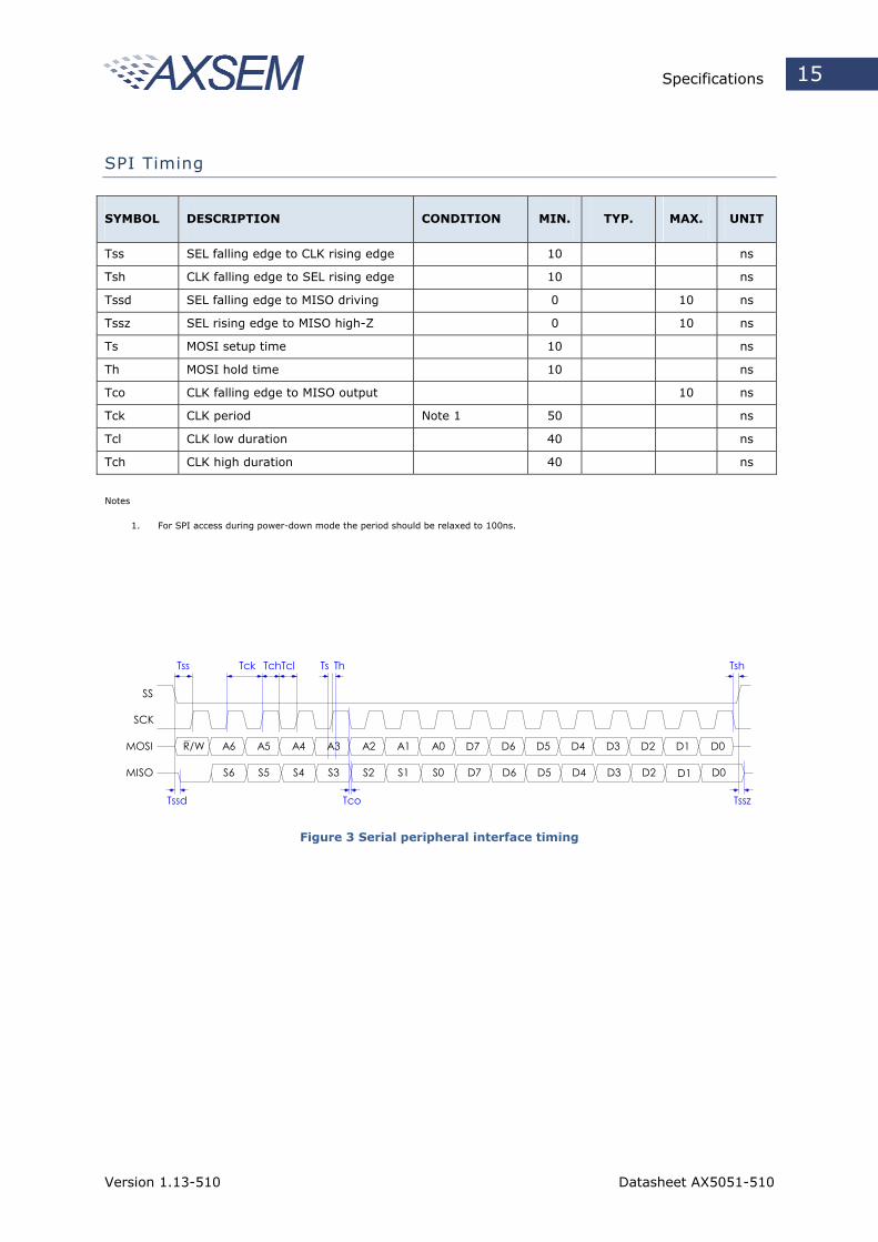
SPI Timing
SYMBOL DESCRIPTION CONDITION MIN. TYP. MAX. UNIT
Tss SEL falling edge to CLK rising edge 10 ns
Tsh CLK falling edge to SEL rising edge 10 ns
Tssd SEL falling edge to MISO driving 0 10 ns
Tssz SEL rising edge to MISO high-Z 0 10 ns
Ts MOSI setup time 10 ns
Th MOSI hold time 10 ns
Tco CLK falling edge to MISO output 10 ns
Tck CLK period Note 1 50 ns
Tcl CLK low duration 40 ns
Tch CLK high duration 40 ns
Notes
1. For SPI access during power-down mode the period should be relaxed to 100ns.
Tsh
R/W
SS
SCK
MOSI
MISO
A6 A5 A4 A3 A2 A1 D7A0 D6 D5 D4 D0D1D2D3
D7 D6 D5 D4 D3 D2 D1 D0S6 S5 S4 S3 S2 S1 S0
Tssd Tco
Tss Tck TchTcl ThTs
Tssz
Figure 3 Serial peripheral interface timing
Version 1.13-510 Datasheet AX5051-510

Life Support Applications 16
5. Life Support Applications
This product is not designed for use in life support appliances, devices, or in systems where malfunction of this product can reasonably be expected to result in personal injury. AXSEM customers using or selling this product for use in such applications do so at their own risk and agree to fully indemnify AXSEM for any damages resulting from such improper use or sale.
Version 1.13-510 Datasheet AX5051-510

Contact Information 17
6. Contact Information
AXSEM AG Oskar-Bider-Strasse 1 CH-8600 Dübendorf SWITZERLAND
Phone +41 44 882 17 07 Fax +41 44 882 17 09 Email [email protected] www.axsem.com
For further product related or sales information please visit our website or contact your local representative.
The specifications in this document are subject to change at AXSEM's discretion. AXSEM assumes no responsibility for any claims or damages arising out of the use of thisdocument, or from the use of products based on this document, including but not limited to claims or damages based on infringement of patents, copyrights or other intellectualproperty rights. AXSEM makes no warranties, either expressed or implied with respect to the information and specifications contained in this document. AXSEM does not supportany applications in connection with life support and commercial aircraft. Performance characteristics listed in this document are estimates only and do not constitute a warranty orguarantee of product performance. The copying, distribution and utilization of this document as well as the communication of its contents to others without expressed authorizationis prohibited. Offenders will be held liable for the payment of damages. All rights reserved. Copyright © 2007-2012 AXSEM AG
Version 1.13-510 Datasheet AX5051-510