axi ethernet lite mac v3 - xilinx - all programmable ethernet lite mac v3.0 2 pg135 november 18,...
TRANSCRIPT

AXI Ethernet Lite MAC v3.0
LogiCORE IP Product Guide
Vivado Design Suite
PG135 November 18, 2015

AXI Ethernet Lite MAC v3.0 www.xilinx.com 2PG135 November 18, 2015
Table of ContentsIP Facts
Chapter 1: OverviewBlock Descriptions . . . . . . . . . . . . . . . . . . . . . . . . . . . . . . . . . . . . . . . . . . . . . . . . . . . . . . . . . . . . . . . . . 6Feature Summary. . . . . . . . . . . . . . . . . . . . . . . . . . . . . . . . . . . . . . . . . . . . . . . . . . . . . . . . . . . . . . . . . . 7Unsupported Features. . . . . . . . . . . . . . . . . . . . . . . . . . . . . . . . . . . . . . . . . . . . . . . . . . . . . . . . . . . . . . 7Licensing and Ordering Information . . . . . . . . . . . . . . . . . . . . . . . . . . . . . . . . . . . . . . . . . . . . . . . . . . . 8
Chapter 2: Product SpecificationPerformance. . . . . . . . . . . . . . . . . . . . . . . . . . . . . . . . . . . . . . . . . . . . . . . . . . . . . . . . . . . . . . . . . . . . . . 9Resource Utilization. . . . . . . . . . . . . . . . . . . . . . . . . . . . . . . . . . . . . . . . . . . . . . . . . . . . . . . . . . . . . . . . 9Port Descriptions . . . . . . . . . . . . . . . . . . . . . . . . . . . . . . . . . . . . . . . . . . . . . . . . . . . . . . . . . . . . . . . . . 12Register Space . . . . . . . . . . . . . . . . . . . . . . . . . . . . . . . . . . . . . . . . . . . . . . . . . . . . . . . . . . . . . . . . . . . 17
Chapter 3: Designing with the CoreClocks . . . . . . . . . . . . . . . . . . . . . . . . . . . . . . . . . . . . . . . . . . . . . . . . . . . . . . . . . . . . . . . . . . . . . . . . . . 25Resets . . . . . . . . . . . . . . . . . . . . . . . . . . . . . . . . . . . . . . . . . . . . . . . . . . . . . . . . . . . . . . . . . . . . . . . . . . 26Programming Sequence. . . . . . . . . . . . . . . . . . . . . . . . . . . . . . . . . . . . . . . . . . . . . . . . . . . . . . . . . . . . 27Management Data Input/Output (MDIO) Master Interface. . . . . . . . . . . . . . . . . . . . . . . . . . . . . . . 32Ethernet Protocol. . . . . . . . . . . . . . . . . . . . . . . . . . . . . . . . . . . . . . . . . . . . . . . . . . . . . . . . . . . . . . . . . 33
Chapter 4: Design Flow StepsCustomizing and Generating the Core . . . . . . . . . . . . . . . . . . . . . . . . . . . . . . . . . . . . . . . . . . . . . . . . 41Constraining the Core . . . . . . . . . . . . . . . . . . . . . . . . . . . . . . . . . . . . . . . . . . . . . . . . . . . . . . . . . . . . . 44Simulation . . . . . . . . . . . . . . . . . . . . . . . . . . . . . . . . . . . . . . . . . . . . . . . . . . . . . . . . . . . . . . . . . . . . . . 45Synthesis and Implementation . . . . . . . . . . . . . . . . . . . . . . . . . . . . . . . . . . . . . . . . . . . . . . . . . . . . . . 45
Chapter 5: Example DesignDirectory and File Contents. . . . . . . . . . . . . . . . . . . . . . . . . . . . . . . . . . . . . . . . . . . . . . . . . . . . . . . . . 46Example Design . . . . . . . . . . . . . . . . . . . . . . . . . . . . . . . . . . . . . . . . . . . . . . . . . . . . . . . . . . . . . . . . . . 48
Chapter 6: Test BenchSimulating the Example Design. . . . . . . . . . . . . . . . . . . . . . . . . . . . . . . . . . . . . . . . . . . . . . . . . . . . . . 54
Send Feedback

AXI Ethernet Lite MAC v3.0 www.xilinx.com 3PG135 November 18, 2015
Appendix A: Migrating and UpgradingMigrating to the Vivado Design Suite. . . . . . . . . . . . . . . . . . . . . . . . . . . . . . . . . . . . . . . . . . . . . . . . . 55Upgrading in the Vivado Design Suite . . . . . . . . . . . . . . . . . . . . . . . . . . . . . . . . . . . . . . . . . . . . . . . . 55
Appendix B: DebuggingFinding Help on Xilinx.com . . . . . . . . . . . . . . . . . . . . . . . . . . . . . . . . . . . . . . . . . . . . . . . . . . . . . . . . . 56Vivado Lab Tools . . . . . . . . . . . . . . . . . . . . . . . . . . . . . . . . . . . . . . . . . . . . . . . . . . . . . . . . . . . . . . . . . 58Hardware Debug . . . . . . . . . . . . . . . . . . . . . . . . . . . . . . . . . . . . . . . . . . . . . . . . . . . . . . . . . . . . . . . . . 58
Appendix C: Additional Resources and Legal NoticesXilinx Resources . . . . . . . . . . . . . . . . . . . . . . . . . . . . . . . . . . . . . . . . . . . . . . . . . . . . . . . . . . . . . . . . . . 59References . . . . . . . . . . . . . . . . . . . . . . . . . . . . . . . . . . . . . . . . . . . . . . . . . . . . . . . . . . . . . . . . . . . . . . 59Revision History . . . . . . . . . . . . . . . . . . . . . . . . . . . . . . . . . . . . . . . . . . . . . . . . . . . . . . . . . . . . . . . . . . 60Please Read: Important Legal Notices . . . . . . . . . . . . . . . . . . . . . . . . . . . . . . . . . . . . . . . . . . . . . . . . 60
Send Feedback
AXI Ethernet Lite MAC v3.0 www.xilinx.com 4PG135 November 18, 2015 Product Specification
IntroductionThe Xilinx® LogiCORE™ IP AXI Ethernet Lite Media Access Controller (MAC) core is designed to incorporate the applicable features described in the IEEE Std. 802.3 Media Independent Interface (MII) specification. It communicates with the processor using the AXI4 or AXI4-Lite interface.
The design provides a 10 Mb/s and 100 Mb/s (also known as Fast Ethernet) interface.
Features• Parameterized AXI4 slave interface based
on the AXI4 or AXI4-Lite specification for transmit and receive data dual port memory access
• Media Independent Interface (MII) for connection to external 10/100 Mb/s PHY transceivers
• Independent internal 2K byte TX and RX dual port memory for holding data for one packet
• Optional dual buffer memories, 4K byte ping-pong, for TX and RX
• Receive and Transmit Interrupts support
• Optional Management Data Input/Output (MDIO) interface for PHY access
• Internal loopback support
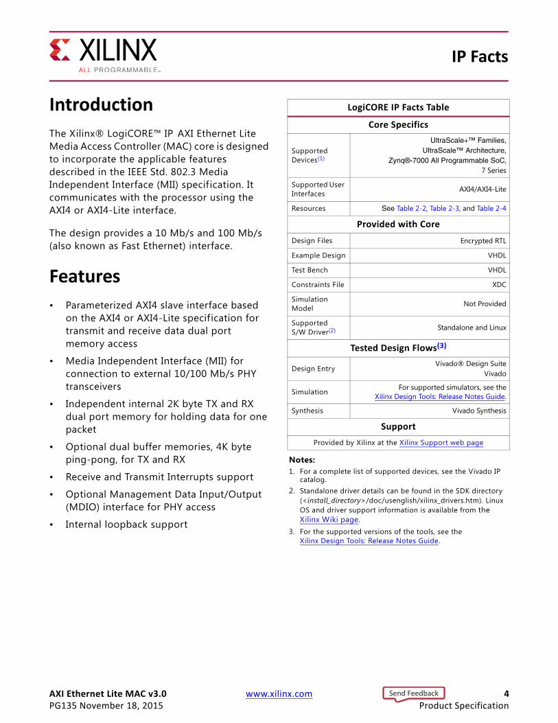
IP Facts
LogiCORE IP Facts Table
Core Specifics
Supported Devices(1)
UltraScale+™ Families,UltraScale™ Architecture,
Zynq®-7000 All Programmable SoC,7 Series
Supported User Interfaces AXI4/AXI4-Lite
Resources See Table 2-2, Table 2-3, and Table 2-4
Provided with CoreDesign Files Encrypted RTL
Example Design VHDL
Test Bench VHDL
Constraints File XDC
Simulation Model Not Provided
Supported S/W Driver(2) Standalone and Linux
Tested Design Flows(3)
Design EntryVivado® Design Suite
Vivado
Simulation For supported simulators, see theXilinx Design Tools: Release Notes Guide.
Synthesis Vivado Synthesis
SupportProvided by Xilinx at the Xilinx Support web page
Notes: 1. For a complete list of supported devices, see the Vivado IP
catalog.2. Standalone driver details can be found in the SDK directory
(<install_directory>/doc/usenglish/xilinx_drivers.htm). Linux OS and driver support information is available from the Xilinx Wiki page.
3. For the supported versions of the tools, see theXilinx Design Tools: Release Notes Guide.
Send Feedback

AXI Ethernet Lite MAC v3.0 www.xilinx.com 5PG135 November 18, 2015
Chapter 1
OverviewThe top-level block diagram of the AXI Ethernet Lite MAC is shown in Figure 1-1.
X-Ref Target - Figure 1-1
Figure 1-1: Block Diagram of the AXI Ethernet Lite MAC
Send Feedback

AXI Ethernet Lite MAC v3.0 www.xilinx.com 6PG135 November 18, 2015
Chapter 1: Overview
Block Descriptions
AXI4 InterfaceThis block provides the AXI4 slave interface for register access and data transfer.
TX BufferThe TX Buffer block consists of 2K byte dual port memory to hold transmit data for one complete frame and the transmit interface control registers. It also includes optional 2K byte dual port memory for the pong buffer based on the parameter Number of Transmit Buffers.
RX BufferThe RX Buffer block consists of 2K dual port memory to hold receive data for one complete frame and the receive interface control register. It also includes optional 2K dual port memory for the pong buffer based on the parameter Number of Receive Buffers.
Transmit This block consists of transmit logic, Cyclic Redundancy Check (CRC) generator module, transmit data MUX, TX First In First Out (FIFO) and the transmit interface module. The CRC generator module calculates the CRC for the frame to be transmitted. The transmit control MUX arranges this frame and sends the preamble, Start-of-Frame Delimiter (SFD), frame data, padding and CRC to the transmit FIFO in the required order. When the frame is transmitted to the PHY, this module generates a transmit interrupt and updates the transmit control register.
ReceiverThis block consists of the RX interface, loopback control MUX, RX FIFO, CRC checker and Receive Control module. Receive data signals from the PHY are passed through the loopback control MUX and stored in the RX FIFO. If loopback is enabled, data on the TX lines is passed to the RX FIFO. The CRC checker module calculates the CRC of the received frame and if the correct CRC is found, receive control logic generates the frame receive interrupt.
MDIO Master InterfaceThe MDIO Master Interface block is included in the design if the parameter Enable MII Management Module is checked in the Vivado® Integrated Design Environment (IDE).
Send Feedback

AXI Ethernet Lite MAC v3.0 www.xilinx.com 7PG135 November 18, 2015
Chapter 1: Overview
This module provides access to the PHY register for PHY management. The MDIO interface is described in PHY Interface Signals in Chapter 2.
Feature Summary• Parameterized AXI4 slave interface based on the AXI4 or AXI4-Lite specif ication for
transmit and receive data dual port memory access
• Media Independent Interface (MII) for connection to external 10/100 Mb/s PHY transceivers
• Independent internal 2K byte TX and RX dual port memory for holding data for one packet
• Optional dual buffer memories, 4K byte ping-pong, for TX and RX
• Receive and Transmit Interrupts
• Optional Management Data Input/Output (MDIO) interface for PHY access
• Internal loopback support
• Accepts messages addressed to its unicast address and the broadcast address.
Unsupported Features• AXI data bus width greater than 32 bits
• AXI address bus width other than 32 bits
• AXI exclusive accesses
• AXI Trustzone
• AXI low-power interface
• AXI narrow transfers
• AXI FIXED, WRAP transactions
• AXI barrier transactions
• AXI debug transactions
• AXI user signals
Send Feedback

AXI Ethernet Lite MAC v3.0 www.xilinx.com 8PG135 November 18, 2015
Chapter 1: Overview
Licensing and Ordering InformationThis Xilinx® LogiCORE™ IP module is provided at no additional cost with the Xilinx Vivado Design Suite under the terms of the Xilinx End User License. Information about this and other Xilinx LogiCORE IP modules is available at the Xilinx Intellectual Property page. For information about pricing and availability of other Xilinx LogiCORE IP modules and tools, contact your local Xilinx sales representative.
Send Feedback

AXI Ethernet Lite MAC v3.0 www.xilinx.com 9PG135 November 18, 2015
Chapter 2
Product Specification
PerformanceThe AXI Ethernet Lite core is characterized as per the benchmarking methodology described in the Vivado Design Suite User Guide: Designing with IP (UG896) [Ref 1]. Table 2-1 shows the results of the characterization runs.
Resource Utilization
The AXI Ethernet Lite resource utilization for various parameter combinations measured with Virtex®-7 FPGA (Table 2-2), Kintex®-7 FPGA (Table 2-3), and Artix®-7 FPGA (Table 2-4) target device.
Table 2-1: Maximum Frequencies
Family Speed GradeFMax (MHz)
AXI4 AXI4-Lite
Virtex-7
-1
200 180
Kintex-7 200 180
Artix-7 150 120
Virtex-7
-2
240 200
Kintex-7 240 200
Artix-7 180 140
Virtex-7
-3
280 220
Kintex-7 280 220
Artix-7 200 160
Send Feedback

AXI Ethernet Lite MAC v3.0 www.xilinx.com 10PG135 November 18, 2015
Chapter 2: Product Specification
Note: Resource numbers for Zynq®-7000 All Programmable SoC and UltraScale™ devices are expected to be similar to 7 series device numbers.
Table 2-2: Resource Estimations for Virtex-7 FPGAsFu
ll Du
plex
Inte
rnal
Loo
pbac
k
Num
ber o
f Rec
eive
Buf
fers
Num
ber o
f Tra
nsfe
r Buf
fers
Enab
le M
II
Enab
le G
loba
l Buf
fers
Num
ber o
f Slic
es
Num
ber o
f Flip
-Flo
ps
Num
ber o
f LU
Ts
0 0 0 0 0 0 239 489 513
1 0 1 1 0 0 244 456 494
1 0 1 1 0 0 271 466 532
1 0 0 0 0 0 259 441 473
1 0 1 1 1 0 289 540 572
1 0 1 1 1 0 306 550 662
1 0 0 0 1 1 278 515 519
1 0 0 0 1 1 280 525 561
1 1 0 0 1 0 273 520 525
Table 2-3: Resource Estimations for Kintex 7 FPGAs
Full
Dupl
ex
Inte
rnal
Loo
pbac
k
Num
ber o
f Rec
eive
Buf
fers
Num
ber o
f Tra
nsfe
r Buf
fers
Enab
le M
II
Enab
le G
loba
l Buf
fers
Num
ber o
f Slic
es
Num
ber o
f Flip
-Flo
ps
Num
ber o
f LU
Ts
0 0 0 0 0 0 256 489 500
1 0 1 1 0 0 231 456 494
1 0 1 1 0 0 270 466 534
1 0 0 0 0 0 253 441 472
1 0 1 1 1 0 297 540 572
1 0 1 1 1 0 301 550 608
1 0 0 0 1 0 268 515 517
1 0 0 0 1 1 273 525 562
1 1 0 0 1 0 269 520 532
Send Feedback

AXI Ethernet Lite MAC v3.0 www.xilinx.com 11PG135 November 18, 2015
Chapter 2: Product Specification
Table 2-4: Resource Estimations for Artix 7 FPGAs
Full
Dupl
ex
Inte
rnal
Loo
pbac
k
Num
ber o
f Rec
eive
Buf
fers
Num
ber o
f Tra
nsfe
r Buf
fers
Enab
le M
II
Enab
le G
loba
l Buf
fers
Num
ber o
f Slic
es
Num
ber o
f Flip
-Flo
ps
Num
ber o
f LU
Ts
0 0 0 0 0 0 264 489 518
1 0 1 1 0 0 261 456 516
1 0 1 1 0 0 250 467 500
1 0 0 0 0 0 245 441 492
1 0 1 1 1 0 301 540 607
1 0 1 1 1 0 321 550 636
1 0 0 0 1 0 281 515 542
1 0 0 0 1 1 287 525 580
1 1 0 0 1 0 292 520 547
Send Feedback
AXI Ethernet Lite MAC v3.0 www.xilinx.com 12PG135 November 18, 2015
Chapter 2: Product Specification
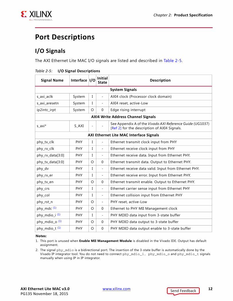
Port Descriptions
I/O SignalsThe AXI Ethernet Lite MAC I/O signals are listed and described in Table 2-5.
Table 2-5: I/O Signal Descriptions
Signal Name Interface I/O InitialState Description
System Signals
s_axi_aclk System I - AXI4 clock (Processor clock domain)
s_axi_aresetn System I - AXI4 reset, active-Low
ip2intc_irpt System O 0 Edge rising interrupt
AXI4 Write Address Channel Signals
s_axi* S_AXI - - See Appendix A of the Vivado AXI Reference Guide (UG1037) [Ref 2] for the description of AXI4 Signals.
AXI Ethernet Lite MAC Interface Signals
phy_tx_clk PHY I - Ethernet transmit clock input from PHY
phy_rx_clk PHY I - Ethernet receive clock input from PHY
phy_rx_data[3:0] PHY I - Ethernet receive data. Input from Ethernet PHY.
phy_tx_data[3:0] PHY O 0 Ethernet transmit data. Output to Ethernet PHY.
phy_dv PHY I - Ethernet receive data valid. Input from Ethernet PHY.
phy_rx_er PHY I - Ethernet receive error. Input from Ethernet PHY.
phy_tx_en PHY O 0 Ethernet transmit enable. Output to Ethernet PHY.
phy_crs PHY I - Ethernet carrier sense input from Ethernet PHY
phy_col PHY I - Ethernet collision input from Ethernet PHY
phy_rst_n PHY O - PHY reset, active-Low
phy_mdc (1) PHY O 0 Ethernet to PHY MII Management clock
phy_mdio_i (1) PHY I - PHY MDIO data input from 3-state buffer
phy_mdio_o (1) PHY O 0 PHY MDIO data output to 3-state buffer
phy_mdio_t (1) PHY O 0 PHY MDIO data output enable to 3-state buffer
Notes: 1. This port is unused when Enable MII Management Module is disabled in the Vivado IDE. Output has default
assignment.2. The signal phy_mdio is a bidirectional port. The insertion of the 3-state buffer is automatically done by the
Vivado IP integrator tool. You do not need to connect phy_mdio_i, phy_mdio_o and phy_mdio_t signals manually when using IP in IP integrator.
Send Feedback

AXI Ethernet Lite MAC v3.0 www.xilinx.com 13PG135 November 18, 2015
Chapter 2: Product Specification
PHY Interface Signals
phy_rst_n
Many PHY devices require that they be held in reset for some period after the power-up sequence. The phy_rst_n signal is an active-Low reset that is tied directly to the AXI reset signal (s_axi_aresetn). This output signal can be connected to the active-Low reset input of a PHY device.
phy_tx_en
The AXI Ethernet Lite MAC uses the Transmit Enable signal (phy_tx_en) to indicate to the PHY that it is providing nibbles at the MII interface for transmission. It is asserted synchronously to phy_tx_clk with the f irst nibble of the preamble and remains asserted while all nibbles are transmitted. Figure 2-1 shows the phy_tx_en timing during a transmission with no collisions.
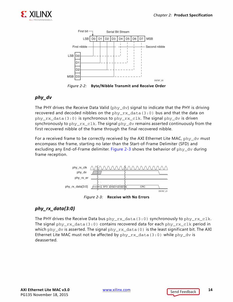
phy_tx_data(3:0)
The AXI Ethernet Lite MAC drives the Transmit Data bus phy_tx_data(3:0) synchronously to phy_tx_clk . The signal phy_tx_data(0) is the least signif icant bit. The PHY transmits the value of phy_tx_data on every clock cycle that phy_tx_en is asserted. The order of the bits, nibbles, and bytes for transmit and receive are shown in Figure 2-2.
X-Ref Target - Figure 2-1
Figure 2-1: Transmission with No Collision
0ns 50ns 100ns 150ns
phy_tx_clk
phy_tx_en
phy_tx_data[3:0]
phy_crs
phy_col
0 0 Preamble SFD D0 D1 CRC 0
DS787_19
Send Feedback
AXI Ethernet Lite MAC v3.0 www.xilinx.com 14PG135 November 18, 2015
Chapter 2: Product Specification
phy_dv
The PHY drives the Receive Data Valid (phy_dv) signal to indicate that the PHY is driving recovered and decoded nibbles on the phy_rx_data(3:0) bus and that the data on phy_rx_data(3:0) is synchronous to phy_rx_clk . The signal phy_dv is driven synchronously to phy_rx_clk . The signal phy_dv remains asserted continuously from the f irst recovered nibble of the frame through the f inal recovered nibble.
For a received frame to be correctly received by the AXI Ethernet Lite MAC, phy_dv must encompass the frame, starting no later than the Start-of-Frame Delimiter (SFD) and excluding any End-of-Frame delimiter. Figure 2-3 shows the behavior of phy_dv during frame reception.
phy_rx_data(3:0)
The PHY drives the Receive Data bus phy_rx_data(3:0) synchronously to phy_rx_clk . The signal phy_rx_data(3:0) contains recovered data for each phy_rx_clk period in which phy_dv is asserted. The signal phy_rx_data(0) is the least signif icant bit. The AXI Ethernet Lite MAC must not be affected by phy_rx_data(3:0) while phy_dv is deasserted.
X-Ref Target - Figure 2-2
Figure 2-2: Byte/Nibble Transmit and Receive Order
Serial Bit Stream First bit
D4 D5 D6 D7 LSB MSB
LSB
MSB
D0
D1
D2
D3
D0 D1 D2 D3
Second nibble First nibble
DS787_20
X-Ref Target - Figure 2-3
Figure 2-3: Receive with No Errors
phy_rx_clk
phy_dv
phy_rx_er
phy_rx_data[3:0] preambl e SFD D0 D1 D2 D3 CRC
DS787_21
Send Feedback

AXI Ethernet Lite MAC v3.0 www.xilinx.com 15PG135 November 18, 2015
Chapter 2: Product Specification
The AXI Ethernet Lite MAC should ignore a special condition that occurs while phy_dv is deasserted; the PHY can provide a False Carrier indication by asserting the phy_rx_er signal while driving the value 1110 onto phy_rx_data(3:0).
phy_rx_er
The PHY drives the Receive Error signal (phy_rx_er) synchronously to phy_rx_clk . The PHY drives phy_rx_er for one or more phy_rx_clk periods to indicate that an error (such as a coding error or any error that the PHY is capable of detecting) was detected somewhere in the frame presently being transferred from the PHY to the AXI Ethernet Lite MAC.
The signal phy_rx_er should have no effect on the AXI Ethernet Lite MAC while phy_dv is deasserted. Figure 2-4 shows the behavior of phy_rx_er during frame reception with errors.
Table 2-6 shows the possible combinations for the receive signals.
X-Ref Target - Figure 2-4
Figure 2-4: Receive with Errors
phy_rx_clk
phy_dv
phy_rx_er
phy_rx_data[3:0] preambl e SFD D0 D1 xx D3 CRC
DS787_22
Table 2-6: Possible Values for phy_dv, phy_rx_er, and phy_rx_data[3:0]
phy_dv phy_rx_er phy_rx_data[3:0] Indication
0 0 0000 through 1111 Normal inter-frame
0 1 0000 Normal inter-frame
0 1 0001 through 1101 Reserved
0 1 1110 False carrier indication
0 1 1111 Reserved
1 0 0000 through 1111 Normal data reception
1 1 0000 through 1111 Data reception with errors
Send Feedback
AXI Ethernet Lite MAC v3.0 www.xilinx.com 16PG135 November 18, 2015
Chapter 2: Product Specification
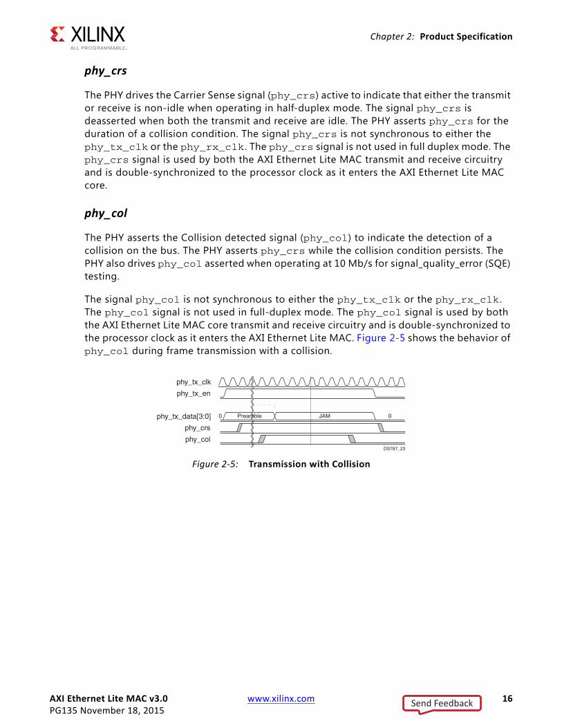
phy_crs
The PHY drives the Carrier Sense signal (phy_crs) active to indicate that either the transmit or receive is non-idle when operating in half-duplex mode. The signal phy_crs is deasserted when both the transmit and receive are idle. The PHY asserts phy_crs for the duration of a collision condition. The signal phy_crs is not synchronous to either the phy_tx_clk or the phy_rx_clk . The phy_crs signal is not used in full duplex mode. The phy_crs signal is used by both the AXI Ethernet Lite MAC transmit and receive circuitry and is double-synchronized to the processor clock as it enters the AXI Ethernet Lite MAC core.
phy_col
The PHY asserts the Collision detected signal (phy_col) to indicate the detection of a collision on the bus. The PHY asserts phy_crs while the collision condition persists. The PHY also drives phy_col asserted when operating at 10 Mb/s for signal_quality_error (SQE) testing.
The signal phy_col is not synchronous to either the phy_tx_clk or the phy_rx_clk . The phy_col signal is not used in full-duplex mode. The phy_col signal is used by both the AXI Ethernet Lite MAC core transmit and receive circuitry and is double-synchronized to the processor clock as it enters the AXI Ethernet Lite MAC. Figure 2-5 shows the behavior of phy_col during frame transmission with a collision.
X-Ref Target - Figure 2-5
Figure 2-5: Transmission with Collision
phy_tx_clk
phy_tx_en
phy_tx_data[3:0]
phy_crs
phy_col
0 Preamble JAM 0
DS787_23
Send Feedback

AXI Ethernet Lite MAC v3.0 www.xilinx.com 17PG135 November 18, 2015
Chapter 2: Product Specification
Register SpaceTable 2-7 shows all the AXI Ethernet Lite MAC core registers and their addresses. Tables 2-8 to 2-17 show the bit allocation and reset values of the registers.
Table 2-7: AXI Ethernet Lite Register Map
Address Offset Register Name Description
07E4h MDIOADDR (1) MDIO address register
07E8h MDIOWR (1) MDIO write data register
07ECh MDIORD (1) MDIO read data register
07F0h MDIOCTRL (1) MDIO control register
07F4h TX Ping Length Transmit length register for ping buffer
07F8h GIE Global interrupt register
07FCh TX Ping Control Transmit control register for ping buffer
0FF4h TX Pong Length (2) Transmit length register for pong buffer
0FFCh TX Pong Control (2) Transmit control register for pong buffer
17FCh RX Ping Control Receive control register for ping buffer
1FFCh RX Pong Control (3) Receive control register for pong buffer
Notes: 1. These registers are included only if Enable MII Management Module is set in the Vivado IDE. 2. These registers are included only if Enable Transmit Buffers is set in the Vivado IDE.3. These registers are included only if Enable Receive Buffers is set in the Vivado IDE.
Send Feedback

AXI Ethernet Lite MAC v3.0 www.xilinx.com 18PG135 November 18, 2015
Chapter 2: Product Specification
Transmit Length Register
The Transmit Length register is a 32-bit read/write register (Figure 2-6). This register is used to store the length (in bytes) of the transmit data stored in dual port memory. The higher 8 bits of the length value should be stored in data bits 15 to 8, while the lower 8 bits should be stored in data bits 7 to 0. The bit definition of this register for the ping and pong buffer interface is shown in Table 2-8.
Global Interrupt Enable Register (GIE)
The Global Interrupt Enable register is a 32-bit read/write register (Figure 2-7). The Global Interrupt Enable Register provides the master enable/disable for the interrupt output (IP2Intc_Irpt signal) to the processor. The bit definition of this register is shown in Table 2-9.
X-Ref Target - Figure 2-6
Figure 2-6: Transmit Length Register
Table 2-8: Transmit Length Register (0x07F4),(0x0FF4)
Bits Name Access Reset value Description
31:16 Reserved N/A N/A Reserved
15:8 MSB Read/Write 0 The higher 8 bits of the frame length
7:0 LSB Read/Write 0 The lower 8 bits of the frame length
31 16 15 0
ReservedFrame Length LSB
Frame Length MSB
8 7
DS787_05
X-Ref Target - Figure 2-7
Figure 2-7: Global Interrupt Enable
Table 2-9: Global Interrupt Enable Register (0x07F8)
Bits Name Access Reset value Description
31 GIE Read/Write 0 Global Interrupt Enable bit
30:0 Reserved N/A N/A Reserved
31 30 0
Global Interrupt Enable (GIE) Reserved
DS787_06
Send Feedback

AXI Ethernet Lite MAC v3.0 www.xilinx.com 19PG135 November 18, 2015
Chapter 2: Product Specification
Transmit Control Register (Ping)
The Transmit Control register for the ping buffer is a 32-bit read/write register (Figure 2-8). This register is used to enable the global interrupt, internal loopback and to initiate transmit transactions. The bit definition of this register is shown in Table 2-10.
X-Ref Target - Figure 2-8
Figure 2-8: Transmit Control Register (Ping)
Table 2-10: Transmit Control Register (0x07FC)
Bits Name Access Reset value Description
31:5 Reserved N/A N/A Reserved
4 Loopback (1) Read/Write 0Internal loopback enable bit0 – No internal loopback1 – Internal loopback enable
3 Interrupt Enable Read/Write 0
Transmit Interrupt Enable bit0 – Disable transmit interrupt1 – Enable transmit interrupt
2 Reserved N/A N/A Reserved
1 Program Read/Write 0
AXI Ethernet Lite MAC address program bit. Setting this bit and status bit configures the new Ethernet MAC address for the core as described in Ethernet MAC Address in Chapter 3.
0 Status Read/Write 0
Transmit ping buffer status indicator 0 –Transmit ping buffer is ready to accept new frame1 – Frame transfer is in progress. Setting this bit initiates transmit transaction. When transmit is complete, the AXI Ethernet Lite MAC core clears this bit.
1. Internal Loopback is supported only in full duplex operation mode. Write to this bit is only valid when, Internal Loopback is enabled from the Vivado IDE options.
05
Reserved Status(S)
Program(P)
134 2
Interrupt Enable (I)
Loopback (L)
31
DS787_07
Reserved
Send Feedback

AXI Ethernet Lite MAC v3.0 www.xilinx.com 20PG135 November 18, 2015
Chapter 2: Product Specification
Transmit Control Register (Pong)
The Transmit Control register for the pong buffer is a 32-bit read/write register (Figure 2-9). This register is used for Ethernet MAC address programming and to initiate transmit transaction from the pong buffer. The bit definition of this register is shown in Table 2-11.
X-Ref Target - Figure 2-9
Figure 2-9: Transmit Control Register (Pong)
Table 2-11: Transmit Control Register (0x0FFC)
Bits Name Access Reset value Description
31:2 Reserved N/A N/A Reserved
1 Program Read/Write 0
AXI Ethernet Lite MAC address program bit. Setting this bit and status bit configures the new Ethernet MAC address for the core as described in Ethernet MAC Address in Chapter 3.
0 Status Read/Write 0
Transmit pong buffer status indicator 0 – Transmit pong buffer is ready to accept a new frame1 – Frame transfer is in progress. Setting this bit initiatestransmit transaction. When transmit is complete, the EthernetLite Ethernet MAC core clears this bit.
0
Reserved Status(S)
Program(P)
1231
DS787_08
Send Feedback

AXI Ethernet Lite MAC v3.0 www.xilinx.com 21PG135 November 18, 2015
Chapter 2: Product Specification
Receive Control Register (Ping)
The Receive Control register for the ping buffer is a 32-bit read/write register (Figure 2-10). This register indicates whether there is a new packet in the ping buffer. The bit definition of this register is shown in Table 2-12.
Receive Control Register (Pong)
The Receive Control register for the pong buffer is a 32-bit read/write register (Figure 2-11). This register indicates whether there is a new packet in the pong buffer. The bit definition of this register is shown in Table 2-13.
X-Ref Target - Figure 2-10
Figure 2-10: Receive Control Register (Ping)
0
Reserved Status(S)
134 2
Interrupt Enable (I)
31
DS787Reserved
Reserved
Table 2-12: Receive Control Register (0x17FC)
Bits Name Access Reset value Description
31:4 Reserved N/A N/A Reserved
3 Interrupt Enable Read/Write 0
Receive Interrupt Enable bit0 – Disable receive interrupt1 – Enable receive interrupt
2:1 Reserved N/A N/A Reserved
0 Status Read/Write 0
Receive status indicator 0 – Receive ping buffer is empty. AXI Ethernet Lite MAC can accept new valid packet.1 – Indicates presence of receive packet ready for software processing. When the software reads the packet from the receive ping buffer, the software must clear this bit.
X-Ref Target - Figure 2-11
Figure 2-11: Receive Control Register (Pong)
0
Reserved Status(S)
131
DS787_10
Send Feedback

AXI Ethernet Lite MAC v3.0 www.xilinx.com 22PG135 November 18, 2015
Chapter 2: Product Specification
MDIO Address Register (MDIOADDR)
The MDIOADDR is a 32-bit read/write register (Figure 2-12). This register is used to configure the PHY device address, PHY register address and type of MDIO transaction. The bit definition of this register is shown in Table 2-14.
MDIO Write Data Register (MDIOWR)
The MDIOWR is a 32-bit read/write register (Figure 2-13). This register contains 16-bit data to be written in to the PHY register. The bit definition of this register is shown in Table 2-15.
Table 2-13: Receive Control Register (0x1FFC)
Bits Name Access Reset value Description
31:1 Reserved N/A N/A Reserved
0 Status Read/Write 0
Receive status indicator 0 – Receive pong buffer is empty. AXI Ethernet Lite MAC can accept new available valid packet.1 – Indicates presence of receive packet ready for software processing.When the software reads the packet from the receive pong buffer, the software must clear this bit.
X-Ref Target - Figure 2-12
Figure 2-12: MDIO Address Register
910 4 051131
OPReserved PHY Address Register Address
DS787_11
Table 2-14: MDIO Address Register (0x07E4)
Bits Name Access Reset Value Description
31:11 Reserved N/A N/A Reserved
10 OP Read/Write 0Operation Access Type0 – Write Access1 – Read Access
9:5 PHYADDR Read/Write 0 PHY device address
4:0 REGADDR Read/Write 0 PHY register address
X-Ref Target - Figure 2-13
Figure 2-13: MDIO Write Data Register
31 1516 0
Reserved MDIO Write Data
DS787_12
Send Feedback

AXI Ethernet Lite MAC v3.0 www.xilinx.com 23PG135 November 18, 2015
Chapter 2: Product Specification
MDIO Read Data Register (MDIORD)
The MDIORD is a 32-bit read/write register (Figure 2-14). This register contains 16-bit read data from the PHY register. The bit definition of this register is shown in Table 2-16.
Table 2-15: MDIO Write Data Register (0x07E8)
Bits Name Access Reset Value Description
31:16 Reserved N/A N/A Reserved
15:0 Write Data Read/Write 0 MDIO write data to be written to PHY register
X-Ref Target - Figure 2-14
Figure 2-14: MDIO Read Data Register
31 1516 0
Reserved MDIO Read Data
DS787_13
Table 2-16: MDIO Read Data Register (0x07EC)
Bits Name Access Reset Value Description
31:16 Reserved N/A N/A Reserved
15:0 Read Data Read 0 MDIO read data from the PHY register
Send Feedback
AXI Ethernet Lite MAC v3.0 www.xilinx.com 24PG135 November 18, 2015
Chapter 2: Product Specification
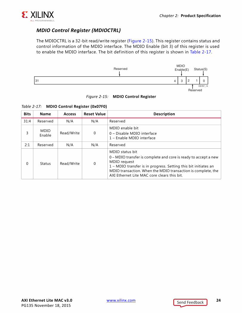
MDIO Control Register (MDIOCTRL)
The MDIOCTRL is a 32-bit read/write register (Figure 2-15). This register contains status and control information of the MDIO interface. The MDIO Enable (bit 3) of this register is used to enable the MDIO interface. The bit definition of this register is shown in Table 2-17.
X-Ref Target - Figure 2-15
Figure 2-15: MDIO Control Register
31 01
Reserved Status(S)
234
MDIOEnable(E)
DS787_14
Reserved
Table 2-17: MDIO Control Register (0x07F0)
Bits Name Access Reset Value Description
31:4 Reserved N/A N/A Reserved
3 MDIO Enable Read/Write 0
MDIO enable bit0 – Disable MDIO interface1 – Enable MDIO interface
2:1 Reserved N/A N/A Reserved
0 Status Read/Write 0
MDIO status bit0 – MDIO transfer is complete and core is ready to accept a new MDIO request1 – MDIO transfer is in progress. Setting this bit initiates an MDIO transaction. When the MDIO transaction is complete, the AXI Ethernet Lite MAC core clears this bit.
Send Feedback
AXI Ethernet Lite MAC v3.0 www.xilinx.com 25PG135 November 18, 2015
Chapter 3
Designing with the CoreThis chapter includes guidelines and additional information to facilitate designing with the core.
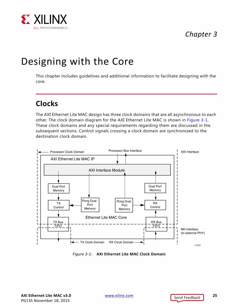
ClocksThe AXI Ethernet Lite MAC design has three clock domains that are all asynchronous to each other. The clock domain diagram for the AXI Ethernet Lite MAC is shown in Figure 3-1. These clock domains and any special requirements regarding them are discussed in the subsequent sections. Control signals crossing a clock domain are synchronized to the destination clock domain.
X-Ref Target - Figure 3-1
Figure 3-1: AXI Ethernet Lite MAC Clock Domain
Send Feedback

AXI Ethernet Lite MAC v3.0 www.xilinx.com 26PG135 November 18, 2015
Chapter 3: Designing with the Core
Transmit ClockThe transmit clock [phy_tx_clk] is generated by the external PHY and must be used by the AXI Ethernet Lite MAC core to provide transmit data [phy_tx_data [3:0]] and to control signals [phy_tx_en] to the PHY.
The PHY provides one clock cycle for each nibble of data transferred resulting in a 2.5 MHz clock for 10BASE-T operation and 25 MHz for 100BASE-T operation at ± 100 ppm with a duty cycle of between 35% and 65%, inclusive. The PHY derives this clock from an external oscillator or crystal.
Receive ClockThe receive clock [phy_rx_clk] is also generated by the external PHY but is derived from the incoming Ethernet traff ic. Similarly to the transmit clock, the PHY provides one clock cycle for each nibble of data transferred, resulting in a 2.5 MHz clock for 10BASE-T operation and 25 MHz for 100BASE-T operation with a duty cycle of between 35% and 65%, inclusive, while incoming data is valid [phy_dv is 1].
The minimum high and low times of the receive clock are at least 35% of the nominal period under all conditions. The receive clock is used by the AXI Ethernet Lite MAC core to sample the receive data [phy_rx_data(3:0)] and control signals [phy_dv and phy_rx_er] from the PHY.
AXI4 Clock (Processor Bus Clock)The majority of the AXI Ethernet Lite MAC operation functions in the processor bus clock domain. This clock must be ≥ 100 MHz to transmit and receive Ethernet data at 100 Mb/s and ≥ 10 MHz to transmit and receive Ethernet data at 10 Mb/s.
ResetsThe AXI Ethernet Lite core works on the s_axi_aresetn, which is active-Low. The reset assertion timing is dependent upon the slowest AXI Ethernet Lite clock. In general allow thirty clock cycles of the slowest AXI Ethernet Lite clock to elapse before accessing the core. Failure to do causes unpredictable behavior.
The phy_rst_n output signal is an active-Low reset that is tied directly to the AXI reset signal (s_axi_aresetn). This signal can be connected to the active-Low reset input of a PHY device.
Send Feedback

AXI Ethernet Lite MAC v3.0 www.xilinx.com 27PG135 November 18, 2015
Chapter 3: Designing with the Core
Programming SequenceThis section contains the following subsections.
• Transmit Interface
• Receive Interface
Transmit InterfaceThe transmit data should be stored in the dual port memory starting at address 0x0. Because of the word aligned addressing, the second four bytes are located at 0x4. The 32-bit interface requires that all four bytes be written at once; there are no individual byte enables within one 32-bit word. The transmit data must include the destination address (6 bytes), the source address (6 bytes), the type/length f ield (2 bytes), and the data field (0 – 1,500 bytes). The preamble, start-of-frame, and CRC should not be included in the dual port memory. The destination, source, type/length, and data must be packed together in contiguous memory.
Dual port memory addresses 0x07F4 is used to store the length (in bytes) of the transmit data stored in dual port memory. The higher 8 bits of the length value should be stored in data bits 15 to 8, while the lower 8 bits should be stored in data bits 7 to 0.
Dual port memory address 0x07F8 is used to set the global interrupt enable (GIE) bit. Setting the GIE = 0 prevents the IP2INTC_Irpt from going active during an interrupt event. Setting GIE = 1 allows the ip2intc_irpt to go active when an interrupt event occurs.
The least two signif icant bits of dual port memory address 0x07FC are control bits (Program or "P" and Status or "S"). The fourth bit (Bit[3] on the data bus) (Transmit Interrupt Enable or "I") is used to enable transmit complete interrupt events. This event is a pulse and occurs when the memory is ready to accept new data. The transmit complete interrupt occurs only if GIE and this bit are both set to 1.
X-Ref Target - Figure 3-2
Figure 3-2: Transmit Dual Port Memory
addr offset0x0
type/length
sourceaddress
datanot
useddestination
address GIE
cont
rol
leng
th
6 6 2 variablevariable (0 - 1500)
addr offset 0x07F4addr offset 0x07F8
addr offset 0x07FC
MD
IO
addr offset 0x07E4 - 0x07F0
16 4 44
1
Note :- 1. MDIO registers are included in the design if the parameter Enable MII Management Module is checked. DS787_15
Send Feedback

AXI Ethernet Lite MAC v3.0 www.xilinx.com 28PG135 November 18, 2015
Chapter 3: Designing with the Core
Software Sequence for Transmit with Ping Buffer
The AXI Ethernet Lite MAC core requires that the length of the transmit data to be stored in address 0x07F4 before the software sets the status bit at offset 0x07FC. The software sequence for initiating a transmit is:
• The software stores the transmit data in the dual port memory starting at address 0x0
• The software writes the length data in the dual port memory at address 0x07F4
• The software writes a 1 to the status bit at address 0x07FC (Bit[0] on the data bus)
• The software monitors the status bit and waits until it is set to 0 by the AXI Ethernet Lite MAC core before initiating another transmit
• If the transmit interrupt and the global interrupt are both enabled, an interrupt occurs when the AXI Ethernet Lite MAC core clears the status bit
• The transmit interrupt, if enabled, also occurs with the completion of writing the Ethernet MAC address
Setting the status bit to a 1 initiates the AXI Ethernet Lite MAC core transmit to perform the following functions:
• Generates the preamble and start-of-frame fields
• Reads the length and the specified amount of data out of the dual port memory according to the length value, adding padding if required
• Detects any collision and performs any jamming, backs off and retries, if necessary
• Calculates the CRC and appends it to the end of the data
• Clears the status bit at the completion of the transmission
• Clearing the status bit causes a transmit complete interrupt, if enabled
Software Sequence for Transmit with Ping-Pong Buffer
If Number of Transmit Buffers is set to 1, two memory buffers exist for the transmit data. The original (ping transmit buffer) remains at the same memory address and controls the global interrupt enable. The second (pong buffer) is mapped at 0x0800 through 0x0FFC. The length and status must be used in the pong buffer the same as in the ping buffer. The I bit and Global Interrupt Enable (GIE) bit are not used from the pong buffer (that is, the I bit and GIE bit of the ping buffer alone control the I bit and GIE bit settings for both buffers). The Ethernet MAC address can be set from the pong buffer. The transmitter always empties the ping buffer f irst after a reset. Then, if data is ready to be transmitted from the pong buffer, that transmission takes place. However, if the pong buffer is not ready to transmit data, the AXI Ethernet Lite MAC core begins to monitor both the ping and pong buffers and transmits the buffer that is ready f irst.
The software sequence for initiating a transmit with both a ping and pong buffer is:
Send Feedback

AXI Ethernet Lite MAC v3.0 www.xilinx.com 29PG135 November 18, 2015
Chapter 3: Designing with the Core
• The software stores the transmit data in the dual port memory starting at address 0x0.
• The software writes the length data in the dual port memory at address 0x07F4.
• The software writes a 1 to the status bit at address 0x07FC (Bit[0] on the data bus).
• The software can write to the pong buffer (0x0800 – 0x0FFC) at any time.
• The software monitors the status bit in the ping buffer and waits until it is set to 0, or waits for a transmit complete interrupt, before filling the ping buffer again.
• If the transmit interrupt and the global interrupt are both enabled, an interrupt occurs when the AXI Ethernet Lite MAC core clears the status bit.
• The transmit interrupt, if enabled, also occurs with the completion of writing the Ethernet MAC address.
Setting the status bit to a 1 initiates the AXI Ethernet Lite MAC core transmit which performs the following functions:
• Generates the preamble and start-of-frame fields
• Reads the length and the specified amount of data out of the dual port memory according to the length value, adding padding if required
• Detects any collision and performs any jamming, backs off, and retries if necessary
• Calculates the CRC and appends it to the end of the data
• Clears the status bit at the completion of the transmission
• Clearing the status bit causes a transmit complete interrupt if enabled
• The hardware then transmits the pong buffer if it is available, or begins monitoring both ping and pong buffers until data is available
Ethernet MAC Address
The 48-bit Ethernet MAC address defaults at reset to 00-00-5E-00-FA-CE. This value can be changed by performing an address program operation using the transmit dual port memory.
The software sequence for programming a new Ethernet MAC address is:
• The software loads the new Ethernet MAC address in the transmit dual port memory, starting at address 0x0. The most significant four bytes are stored at address 0x0 and the least significant two bytes are stored at address 0x4. The Ethernet MAC address can also be programmed from the pong buffer starting at 0x0800.
• The software writes a 1 to both the program bit (Bit[1] on the data bus) and the status bit (Bit[0] on the data bus) at address 0x07FC. The pong buffer address is 0x0FFC.
• The software monitors the status and program bits and waits until they are set to 0 before performing any additional Ethernet operations.
Send Feedback

AXI Ethernet Lite MAC v3.0 www.xilinx.com 30PG135 November 18, 2015
Chapter 3: Designing with the Core
A transmit complete interrupt, if enabled, occurs when the status and program bits are cleared
Receive InterfaceThe entire receive frame data from destination address to the end of the CRC is stored in the receive dual port memory area which starts at address 0x1000. The preamble and start-of-frame fields are not stored in dual port memory. Dual port memory address 0x17FC (Bit[0] on the data bus) is used as a status to indicate the presence of a receive packet that is ready for processing by the software.
Dual port memory address 0x17FC (Bit[3] on the data bus) is the Receive Interrupt enable. This event is a pulse and occurs when the memory has data available. The receive complete interrupt occurs only if this bit and GIE are both set to 1.
When the status bit is 0, the AXI Ethernet Lite MAC monitors the Ethernet for packets with a destination address that matches its Ethernet MAC address or the broadcast address. If a packet satisf ies either of these conditions, the packet is received and stored in dual port memory starting at address 0x1000. When the packet has been received, the AXI Ethernet Lite MAC core verif ies the CRC. If the CRC value is correct, the status bit is set. If the CRC bit is incorrect, the status bit is not set and the AXI Ethernet Lite MAC core resumes monitoring the Ethernet bus.
Also, if the AXI Ethernet Lite MAC core receive Runt Frame (frame length less than the 60 Bytes) with a valid CRC, the core does not set the status bit and the interrupt is not generated. When the status bit is set, the AXI Ethernet Lite MAC does not perform any receive operations until the bit has been cleared to 0 by the software, indicating that all of the receive data has been retrieved from the dual port memory.
Software Sequence for Receive with Ping Buffer
The software sequence for processing a receive is:
1. The software monitors the receive status bit until it is set to 1 by the AXI Ethernet Lite MAC core and waits for a receive complete interrupt, if enabled.
2. When the status is set to 1, or a receive complete interrupt has occurred, the software reads the entire receive data out of the dual port memory.
3. The software writes a 0 to the receive status bit enabling the AXI Ethernet Lite MAC core to resume receive processing.
X-Ref Target - Figure 3-3
Figure 3-3: Receive Dual Port Memory
addr offset 0x0
addr offset0x17FC
type/ length
source address
data not
used destination
address
cont
rol
6 6 2 variablevariable (0 - 1500) 4
CRC
4
DS787_16
Send Feedback

AXI Ethernet Lite MAC v3.0 www.xilinx.com 31PG135 November 18, 2015
Chapter 3: Designing with the Core
Software Sequence for Receive Ping-Pong
If Number of Receive Buffers is set to 1 then two memory buffers exist for the receive data. The original (ping receive buffer) remains at the same memory location. The second (pong receiver buffer) is mapped to 0x1800 through 0x1FFC. Data is stored the same way in the pong buffer as it is in the ping buffer.
The software sequence for processing a receive packet(s) with Number of Receive Buffers = 1 is:
1. The software monitors the ping receive status bit until it is set to 1 by the AXI Ethernet Lite MAC, or waits for a receive complete interrupt, if enabled.
2. When the ping status is set to 1, or a receive complete interrupt has occurred, the software reads the entire receive data out of the ping dual port memory.
3. The AXI Ethernet Lite MAC receives the next packet and stores it in the pong receive buffer.
4. The software writes a 0 to the ping receive status bit, enabling the AXI Ethernet Lite MAC core to receive another packet in the ping receive buffer.
5. The software monitors the pong receive status bit until it is set to 1 by the AXI Ethernet Lite MAC core, or waits for a receive complete interrupt, if enabled.
6. When the pong status is set to 1, or a receive complete interrupt has occurred, the software reads the entire receive data out of the ping dual port memory.
7. The hardware always writes the f irst received packet, after a reset, to the ping buffer; the second received packet is written to the pong buffer and the third received packet is written to the ping buffer, and so forth.
IMPORTANT: Not clearing the status bit of ping and pong buffer results in packet loss.For example, after correctly receiving two packet status bits of both ping and pong, buffers are set to 1 by the AXI Ethernet Lite MAC. If software only clears status bit of pong buffer, then the third packet would be lost (as this packet is intended to be received by ping buffer but its status bit is not cleared) and the IP would correctly receive the fourth packet.
Send Feedback

AXI Ethernet Lite MAC v3.0 www.xilinx.com 32PG135 November 18, 2015
Chapter 3: Designing with the Core
Management Data Input/Output (MDIO) Master InterfaceThe Management Data Input/Output Master Interface is included in the design if the parameter Enable MII Management Module is checked in the Vivado® Integrated Design Environment (IDE). Including this logic allows AXI Ethernet Lite MAC core to access PHY configuration registers. The MDIO Master Interface module is designed to incorporate the features described in IEEE 802.3 Media Independent Interface (MII) specif ication.
The MDIO module generates management data clock to the PHY (phy_mdc) with a minimum period of 400 ns. The signal phy_mdc is sourced to PHY as timing reference for transfer of information on the phy_mdio (Management Data Input/Output) data signal.
The phy_mdio signal is a bidirectional signal between the PHY and MDIO module. It is used to transfer control and status information between the PHY and the MDIO module. The control information is driven by the MDIO module synchronously with respect to phy_mdc and is sampled synchronously by the PHY. The status information is driven by the PHY synchronously with respect to phy_mdc and is sampled synchronously by the MDIO module. The signal phy_mdio is driven through a 3-state circuit that enables either the MDIO module or the PHY to drive the circuit.
The MDIO interface uses a standard method to access PHY management registers. The MDIO module supports up to 32 PHY devices. To access each PHY device, the PHY device address must be written into the MDIO Address (MDIOADDR) register followed by PHY register address (Figure 2-12). This module supports access to up to 32 PHY management registers. The write transaction data for the PHY must be written into MDIO Write Data (MDIOWR) register and the status data from the PHY register can be read from the MDIO Read Data (MDIORD) register. The MDIO Control (MDIOCTRL) register is used to initiate to management transaction on the MDIO lines.
The AXI Ethernet Lite MAC requires that the PHY device address and PHY register address be stored in the MDIO Address Register at address 0x07E4 before the software sets the status bit in the MDIO Control Register at offset 0x07F0.
The software sequence for initiating a PHY register write transaction is:
1. The software reads the MDIOCTRL register to verify if the MDIO master is busy executing a previous request. If the status bit is 0, the MDIO master can accept a new request.
2. The software stores the PHY device address and PHY register address and writes 0 to Bit[10] in the MDIOADDR register at address 0x07E4.
3. The software stores the PHY register write data in the MDIOWR register at address 0x07E8.
Send Feedback

AXI Ethernet Lite MAC v3.0 www.xilinx.com 33PG135 November 18, 2015
Chapter 3: Designing with the Core
4. The software writes 1 in the MDIO enable bit in the MDIOCTRL register at address 0x07F0.
5. The software writes a 1 to the status bit at address 0x07F0 (Bit[0] on the data bus) to start the MDIO transaction.
6. After completing the MDIO write transaction, the AXI Ethernet Lite MAC core clears the status bit.
7. The software monitors the status bit and waits until it is set to 0 by the AXI Ethernet Lite MAC before initiating new transaction on the MDIO lines.
The software sequence for initiating a PHY register read transaction is:
1. The software reads the MDIOCTRL register to verify if the MDIO master is busy executing a previous request. If the status bit is 0, the MDIO master can accept a new request.
2. The software stores the PHY device address and PHY register address and writes 1 to bit 10 in the MDIOADDR register at address 0x07E4.
3. The software writes 1 in the MDIO enable bit in the MDIOCTRL register at address 0x07F0.
4. The software writes a 1 to the status bit at address 0x07F0 (bit 0 on the data bus) to start the MDIO transaction.
5. After completing the MDIO Read transaction, the AXI Ethernet Lite MAC core clears the status bit.
The software monitors the status bit and waits until it is set to 0 by the AXI Ethernet Lite MAC core before initiating a new transaction on the MDIO lines.
Ethernet ProtocolEthernet data is encapsulated in frames (Figure 3-4). The f ields and bits in the frame are transmitted from left to right (from the least signif icant bit to the most significant bit), unless specif ied otherwise.
PreambleThe preamble field is used for synchronization and must contain seven bytes with the pattern 10101010. If a collision is detected during the transmission of the preamble or start-of-frame delimiter f ields, the transmission of both f ields is completed.
Send Feedback

AXI Ethernet Lite MAC v3.0 www.xilinx.com 34PG135 November 18, 2015
Chapter 3: Designing with the Core
For transmission, this f ield is always automatically inserted by the AXI Ethernet Lite MAC core and should never appear in the packet data provided to the AXI Ethernet Lite MAC core. For reception, this f ield is always stripped from the packet data. The AXI Ethernet Lite MAC design does not support the Ethernet 8-byte preamble frame type.
Start Frame DelimiterThe start frame delimiter f ield marks the start of the frame and must contain the pattern 10101011. If a collision is detected during the transmission of the preamble or start-of-frame delimiter f ields, the transmission of both f ields is completed.
The receive data valid signal from the PHY (phy_dv) can go active during the preamble but is active prior to the start frame delimiter f ield. For transmission, this f ield is always automatically inserted by the AXI Ethernet Lite MAC core and should never appear in the packet data provided to the AXI Ethernet Lite MAC core. For reception, this f ield is always stripped from the packet data.
Destination AddressThe destination address field is 6 bytes in length. The least signif icant bit of the destination address is used to determine if the address is an individual/unicast (0) or group/multicast (1) address. Multicast addresses are used to group logically related stations.
The broadcast address (destination address f ield is all 1s) is a multicast address that addresses all stations on the LAN. The AXI Ethernet Lite MAC supports transmission and reception of unicast and broadcast packets. The AXI Ethernet Lite MAC core does not support multicast packets. This f ield is always provided in the packet data for transmissions and is always retained in the receive packet data.
Note: The AXI Ethernet Lite MAC design does not support 16-bit destination addresses as defined in the IEEE 802 standard.
Source AddressThe source address f ield is 6 bytes in length. This f ield is always provided in the packet data for transmissions and is always retained in the receive packet data.
Note: The AXI Ethernet Lite MAC design does not support 16-bit source addresses as defined in the IEEE 802 standard.
Type/LengthThe type/length f ield is 2 bytes in length. When used as a length f ield, the value in this f ield represents the number of bytes in the subsequent data field. This value does not include any bytes that might have been inserted in the padding field following the data field. The value of this f ield determines if it should be interpreted as a length as defined by the IEEE 802.3 standard or a type f ield as defined by the Ethernet protocol.
Send Feedback

AXI Ethernet Lite MAC v3.0 www.xilinx.com 35PG135 November 18, 2015
Chapter 3: Designing with the Core
The maximum length of a data f ield is 1,500 bytes. Therefore, a value in this f ield that exceeds 1,500 (0x05DC) indicates that a frame type rather than a length value is provided in this f ield. The IEEE 802.3 standard uses the value 1536 (0x0600) or greater to signal a type f ield. The AXI Ethernet Lite MAC does not perform any processing of the type/length f ield. This f ield is transmitted with the least signif icant bit f irst but with the high order byte f irst. This f ield is always provided in the packet data for transmissions and is always retained in the receive packet data.
DataThe data f ield can vary from 0 to 1,500 bytes in length. This f ield is always provided in the packet data for transmissions and is always retained in the receive packet data.
PadThe pad field can vary from 0 to 46 bytes in length. This f ield is used to ensure that the frame length is at least 64 bytes in length (the preamble and SFD fields are not considered part of the frame for this calculation) which is required for successful Carrier Sense Multiple Access with Collision Detection (CSMA/CD) operation. The values in this f ield are used in the frame check sequence calculation but are not included in the length f ield value if it is used. The length of this f ield and the data field combined must be at least 46 bytes. If the data f ield contains 0 bytes, the pad field is 46 bytes. If the data field is 46 bytes or more, the pad f ield has 0 bytes. For transmission, this f ield is inserted automatically by the AXI Ethernet Lite MAC if required to meet the minimum length requirement. If present in the receive packet, this f ield is always retained in the receive packet data.
FCSThe Frame Check Sequence (FCS) f ield is 4 bytes in length. The value of the FCS f ield is calculated over the source address, destination address, length/type, data, and pad f ields using a 32-bit CRC defined in paragraph 3.2.8 of [Ref 3]:
G(x) = x32 + x26 + x23 + x22 + x16 + x12 + x11 + x10 + x8 + x7 + x5 + x4 + x2 + x1 + x0
The CRC bits are placed in the FCS f ield with the x31 term in the left most bit of the f irst byte and the x0 term is the right most bit of the last byte (that is, the bits of the CRC are transmitted in the order x31, x30,..., x1, x0).
The AXI Ethernet Lite MAC implementation of the CRC algorithm calculates the CRC value a nibble at a time to coincide with the data size exchanged with the external PHY interface for each transmit and receive clock period. For transmission, this f ield is always inserted automatically by the AXI Ethernet Lite MAC core and is always retained in the receive packet data.
Send Feedback

AXI Ethernet Lite MAC v3.0 www.xilinx.com 36PG135 November 18, 2015
Chapter 3: Designing with the Core
Interframe Gap and DeferringNote: Interframe Gap and interframe spacing are used interchangeably and are equivalent.
Frames are transmitted over the serial interface with an interframe gap which is specif ied by the IEEE Std. 802.3 to be 96 bit times (9.6 μs for 10 MHz and 0.96 μs for 100 MHz). The process for deferring is different for half-duplex and full-duplex systems and is as follows:
Half-Duplex
1. Even when it has nothing to transmit, the AXI Ethernet Lite MAC monitors the bus for traffic by watching the carrier sense signal (phy_crs) from the external PHY. Whenever the bus is busy (phy_crs = 1), the AXI Ethernet Lite MAC defers to the passing frame by delaying any pending transmission of its own.
2. After the last bit of the passing frame (when carrier sense signal changes from TRUE to FALSE), the AXI Ethernet Lite MAC starts the timing of the interframe gap.
3. The AXI Ethernet Lite MAC resets the interframe gap timer if the carrier sense becomes TRUE.
Full-Duplex
The AXI Ethernet Lite MAC does not use the carrier sense signal from the external PHY when in full duplex mode because the bus is not shared and only needs to monitor its own transmissions. After the last bit of an AXI Ethernet Lite MAC transmission, the AXI Ethernet Lite MAC starts the timing of the interframe gap.
CSMA/CD MethodA full-duplex Ethernet bus is, by definition, a point-to-point dedicated connection between two Ethernet devices capable of simultaneous transmit and receive with no possibility of collisions.
For a half-duplex Ethernet bus, the CSMA/CD media access method defines how two or more stations share a common bus. To transmit, a station waits (defers) for a quiet period on the bus (no other station is transmitting (phy_crs = 0)) and then starts transmission of its message after the interframe gap period.
X-Ref Target - Figure 3-4
Figure 3-4: Ethernet Data Frame
Preamble Start of FrameDelimiter (SFD)
Destination Address
Source Address
64 - 1518 bytes
Type/Length Data Frame Check
Sequence Pad
7 6 4 2 0 - 1500 0 - 46 6 1
DS787_02
Send Feedback

AXI Ethernet Lite MAC v3.0 www.xilinx.com 37PG135 November 18, 2015
Chapter 3: Designing with the Core
If, after initiating a transmission, the message collides with the message of another station (phy_col - 1), then each transmitting station intentionally continues to transmit (jam) for an additional predefined period (32 bits for 10/100 Mb/s) to ensure propagation of the collision throughout the system. The station remains silent for a random amount of time (back off) before attempting to transmit again. A station can experience a collision during the beginning of its transmission (the collision window) before its transmission has had time to propagate to all stations on the bus. When the collision window has passed, a transmitting station has acquired the bus.
Subsequent collisions (late collisions) are avoided because all other (properly functioning) stations are assumed to have detected the transmission and are deferring to it. The time to acquire the bus is based on the round-trip propagation time of the bus (64 byte times for 10/100 Mb/s).
Transmit FlowThe flowchart in Figure 3-5 shows the high level flow followed for packet transmission.
Send Feedback

AXI Ethernet Lite MAC v3.0 www.xilinx.com 38PG135 November 18, 2015
Chapter 3: Designing with the Core
X-Ref Target - Figure 3-5
Figure 3-5: Transmit Flow
Send Feedback

AXI Ethernet Lite MAC v3.0 www.xilinx.com 39PG135 November 18, 2015
Chapter 3: Designing with the Core
Receive FlowThe flowchart in Figure 3-6 shows the high level flow followed for packet reception.
X-Ref Target - Figure 3-6
Figure 3-6: Receive Flow
Send Feedback

AXI Ethernet Lite MAC v3.0 www.xilinx.com 40PG135 November 18, 2015
Chapter 3: Designing with the Core
Internal Loopback ModeThe AXI Ethernet Lite MAC core can be configured in internal loopback mode by setting the parameter Enable Internal Loopback is checked in the Vivado IDE and by setting bit 4 of the Transmit Control Register (Ping). In loopback mode, the logic uses BUFG for PHY clock switching. In this mode, the AXI Ethernet Lite MAC core routes back data on the TX lines to the RX lines. The loopback mode can be tested only in full duplex mode. In this mode, the core does not accept any data from the PHY and phy_tx_clk and phy_tx_en are used as phy_rx_clk and phy_dv internally (Figure 3-7).
.X-Ref Target - Figure 3-7
Figure 3-7: Internal Loopback Mode
Send Feedback

AXI Ethernet Lite MAC v3.0 www.xilinx.com 41PG135 November 18, 2015
Chapter 4
Design Flow StepsThis chapter describes customizing and generating the core, constraining the core, and the simulation, synthesis and implementation steps that are specific to this IP core. More detailed information about the standard Vivado® design flows and the Vivado IP integrator can be found in the following Vivado Design Suite user guides:
• Vivado Design Suite User Guide: Designing with IP (UG896) [Ref 1]
• Vivado Design Suite User Guide: Designing IP Subsystems using IP Integrator (UG994) [Ref 4]
• Vivado Design Suite User Guide: Getting Started (UG910) [Ref 5]
• Vivado Design Suite User Guide: Logic Simulation (UG900) [Ref 6]
Customizing and Generating the CoreThis section includes information about using Xilinx tools to customize and generate the core in the Vivado Design Suite.
If you are customizing and generating the core in the IP integrator, see the Vivado Design Suite User Guide: Designing IP Subsystems using IP Integrator (UG994) [Ref 4] for detailed information. IP integrator might auto-compute certain configuration values when validating or generating the design. To check whether the values do change, see the description of the parameter in this chapter. To view the parameter value you can run the validate_bd_design command in the Tcl console.
To access the AXI Ethernet Lite, perform the following:
1. Open a project by selecting File > Open Project or create a new project by selecting File > New Project.
2. Open Vivado IP Catalog and choose Embedded Processing/High Speed Peripheral.
3. Double-click AXI Ethernet Lite to display the AXI Ethernet Lite Vivado IDE.
For details, see the Vivado Design Suite User Guide: Designing with IP (UG896) [Ref 1] and the Vivado Design Suite User Guide: Getting Started (UG910) [Ref 5].
Send Feedback

AXI Ethernet Lite MAC v3.0 www.xilinx.com 42PG135 November 18, 2015
Chapter 4: Design Flow Steps
Note: Figure in this chapter is an illustration of the Vivado IDE. This layout might vary from the current version.
Field DescriptionsAll the parameters except ID WIDTH are available in IP integrator. ID Width is auto-computed which means that you are not allowed to override
AXI Interface Parameters
• AXI Protocol
° AXI4 – Enables AXI4 interface
° AXI4LITE – Enables AXI4-Lite interface
• AXI Clock Frequency (in MHz) – AXI Ethernet Lite core frequency. See Table 2-1 for maximum supported frequency.
X-Ref Target - Figure 4-1
Figure 4-1: Vivado IDE
Send Feedback

AXI Ethernet Lite MAC v3.0 www.xilinx.com 43PG135 November 18, 2015
Chapter 4: Design Flow Steps
Ethernet Lite MAC Parameters
• Communication Mode
° Full Duplex – Enables full duplex mode
° Half Duplex – Enables half duplex mode
• Number of Transmit Buffers
° 0 – Enables single TX buffer
° 1 – Enables dual TX buffers
• Number of Receive Buffers
° 0 – Enables single RX buffer
° 1 – Enables dual RX buffers
• Enable Internal Loopback – Configures AXI Ethernet Lite in internal loopback mode when enabled
• Enable Global Buffers for PHY Clocks
Note: Internal loopback is supported only in full duplex mode.
° 0 – Normal Input buffers for PHY Clocks
° 1 – Global buffers for PHY Clocks
• ID Width – ID width of the AXI interface. Allowed values are 0 to 16.
Note: ID Width is auto-computed which means that you are not allowed to override it.
• Enable MII Management Module – Includes MDIO module that provides access to PHY registers when enabled
User ParametersTable 4-1 shows the relationship between the GUI f ields in the Vivado IDE and the User Parameters (which can be viewed in the Tcl Console).
Table 4-1: GUI Parameter to User Parameter Relationship
GUI Parameter/Value(1) User Parameter/Value(1) Default Value(1)
AXI Protocol C_S_AXI_PROTOCOL AXI4LITE
AXI Clock Frequency(2) AXI_ACLK_FREQ_MHZ 100
Communication Mode(3) C_DUPLEX 1
Number of Transmit Buffers C_TX_PING_PONG 1
Number of Receive Buffers C_RX_PING_PONG 1
Enable Internal Loopback(4) C_INCLUDE_INTERNAL_LOOPBACK 0
Enable Global Buffers for PHY Clocks C_INCLUDE_GLOBAL_BUFFERS 1
Send Feedback

AXI Ethernet Lite MAC v3.0 www.xilinx.com 44PG135 November 18, 2015
Chapter 4: Design Flow Steps
Output GenerationFor details, see the Vivado Design Suite User Guide: Designing with IP (UG896) [Ref 1].
Constraining the CoreDesign constraints as applicable are generated along with the other core deliverables in the Vivado Design Suite.
Required ConstraintsThis section is not applicable for this IP core.
Device, Package, and Speed Grade SelectionsThis section is not applicable for this IP core.
Clock FrequenciesThis section is not applicable for this IP core.
Clock ManagementThis section is not applicable for this IP core.
Clock PlacementThis section is not applicable for this IP core.
Enable MII Management Module C_INCLUDE_MDIO 1
ID Width(5) C_S_AXI_ID_WIDTH 0
Notes: 1. Parameter values are listed in the table where the GUI parameter value differs from the user parameter value. Such values are
shown in this table as indented below the associated parameter.2. Clock frequency should be minimum four times of TX/RX clocks.3. Value “0” for Half Duplex and Value “1” for Full Duplex.4. Not applicable when Communication Mode is “0”(Half Duplex), and value should be “0.”5. Applicable only when AXI Protocol is AXI4 (Full).
Table 4-1: GUI Parameter to User Parameter Relationship (Cont’d)
GUI Parameter/Value(1) User Parameter/Value(1) Default Value(1)
Send Feedback

AXI Ethernet Lite MAC v3.0 www.xilinx.com 45PG135 November 18, 2015
Chapter 4: Design Flow Steps
BankingThis section is not applicable for this IP core.
Transceiver PlacementThis section is not applicable for this IP core.
I/O Standard and PlacementThis section is not applicable for this IP core.
SimulationThis section contains information about simulating IP in the Vivado Design Suite. For comprehensive information about Vivado simulation components, as well as information about using supported third-party tools, see the Vivado Design Suite User Guide: Logic Simulation (UG900) [Ref 6].
Synthesis and ImplementationThis section contains information about synthesis and implementation in the Vivado Design Suite. For details about synthesis and implementation, see the Vivado Design Suite User Guide: Designing with IP (UG896) [Ref 1].
Send Feedback

AXI Ethernet Lite MAC v3.0 www.xilinx.com 46PG135 November 18, 2015
Chapter 5
Example DesignThis chapter contains information about the example design provided in the Xilinx® Vivado® Design Suite.
Clicking Open IP Example Design in Vivado IDE (Sources Window on generated IP) or entering the open_example_project command (get_ips <component_name>) in the Tcl console invokes a separate example design project. In this new project <component_name>_exdes> is the top module for synthesis, and <component_name>_exdes_tb> is the top module for simulation. The implementation or simulation of the example design can be run from the example design.
Directory and File Contents
top directory<project_name>/<project_name>.srcs/sources_1/ip/
VHDL Example design, Test bench and coeff icient (COE) f iles. These f iles drive ATG to generate required AXI transactions.
The AXI Ethernetlite core directories and their associated f iles are defined in the following sections.
<project_name>/<project_name>.srcs/sources_1/ip/
Send Feedback

AXI Ethernet Lite MAC v3.0 www.xilinx.com 47PG135 November 18, 2015
Chapter 5: Example Design
The <project directory> contains all the Vivado design tool project f iles.
<project_name>/<project_name>.srcs/sources_1/ip/<component name>
The <component name> directory contains the HDL f iles that implement the core.
example design
The example design directory contains the example design f iles provided with the core.
Table 5-1: project_name>/<project_name>.srcs/sources_1/ip/
Name Description
Synth/<component name>.v|vhd Synthesis wrapper generated by the Vivado design tools
Sim/<component name>.v|vhd Simulation wrapper generated by the Vivado design tools
<component name>.xci Vivado tools project-specif ic option f ile; can be used as an input to the Vivado design tools.
<component name>.vho|veo VHDL or Verilog instantiation template
<component name>_ooc.xdc Out of Context constraints for IP
COE Files
These f iles are intended for the use with the example design. Right-click on the generated IP and select Open Example Design in the Vivado design tools to create the example design project
Table 5-2: Example Design Directory
Name Description
<component name>_exdes.vhd Example design top f ile for synthesis
<component name>_exdes_tb.vhd Example design top f ile for simulation
Exdes.xdc Constrains for Example design
Send Feedback

AXI Ethernet Lite MAC v3.0 www.xilinx.com 48PG135 November 18, 2015
Chapter 5: Example Design
Example DesignThe following sections describe the top-level example design for the AXI Ethernetlite core.
The complete example design works as a mini-system to show the AXI Ethernetlite core functionality by demonstrating the transmit and receive of the Ethernet packet.
Clock GeneratorThe AXI Ethernetlite example design makes use of the clocking wizard to supply clocks and resets to all other blocks in the design.
The clocking wizard is configured to provide two clocks.
• The first output with the frequency value with the option given in Vivado IDE; this is supplied as the primary clock to all blocks in the example design.
• The second output with the frequency 25 MHz which is the input for phy_tx_clk and phy_rx_clk for the AXI Ethernetlite IP core. The locked signal from the wizard is appropriately used as a reset.
AXI Traffic Generator (ATG) The example design makes use of one or two AXI Traffic Generators based upon the AXI protocol selected in Vivado IDE.
• The ATG is used in the example design to write the raw data of the packet to the AXI Ethernetlite IP core and also to read/write the control/status registers of the core. The ATG determines the test pass/fail condition based upon the status read from core.
• One ATG is used in system test mode to control the transaction sequence in all configurations.
• The other ATG is used in AXI4 mode and is only instantiated when the AXI protocol selected is AXI4 for the AXI Ethernetlite core.
The ATG takes four COE f iles as input and provides Done and Status pins as outputs which determine the result of the tests.
Send Feedback

AXI Ethernet Lite MAC v3.0 www.xilinx.com 49PG135 November 18, 2015
Chapter 5: Example Design
Working Example Designs
AXI4-Lite Protocol without Internal Loopback
When the AXI4-Lite protocol is selected without Internal Loopback:
• The ATG in system test mode with two AXI channels enabled is used to write a Destination Address, Source Address, and test data into the 2k Memory present in core.
• The example design programs the registers in the AXI Ethernetlite core to indicate the number of bytes in a packet and to state that data is ready for packet transmission.
• The AXI Ethernetlite IP core generates the Ethernet packet and transmits it through the MII interface.
• Another instance of the AXI Ethernetlite IP core that is used in the example design receivse the Ethernet packet.
• A CRC check that is performed by default in the IP assures the correct reception of the packet and updates the status register to indicate the same.
• The second channel of the ATG is connected to the partner AXI Ethernetlite IP core which reads the status register and gives a test pass/fail condition through the ATG Status and Done pins.
X-Ref Target - Figure 5-1
Figure 5-1: AXI4-Lite Example Design without Internal Loopback
Send Feedback

AXI Ethernet Lite MAC v3.0 www.xilinx.com 50PG135 November 18, 2015
Chapter 5: Example Design
AXI4 Protocol without Internal Loopback
When the AXI4 protocol is selected without Internal Loopback:
• Two ATGs are used: one in AXI4 mode is connected to the AXI Ethernetlite IP core and the other ATG in system test mode is used to configure the ATG Full mode.
• The ATG in system test mode configures another ATG to generate a burst transaction to transfer data into the AXI Ethernetlite IP core TX buffer. The content to be transferred in the AXI burst transaction is also loaded into ATF FULL using the system test mode.
• The ATG then updates the register in the AXI Ethernetlite core to start transmission of Ethernet packets.
• Another instance of the AXI Ethernetlite core that is used in the example design receives the Ethernet packet and updates the status registers based upon the CRC check performed.
• Another instance of ATG FULL connected to the partner IP reads the status and passes it to the ATG in system test mode which determines the test pass/fail condition.
X-Ref Target - Figure 5-2
Figure 5-2: AXI4 Example Design without Internal Loopback
Send Feedback

AXI Ethernet Lite MAC v3.0 www.xilinx.com 51PG135 November 18, 2015
Chapter 5: Example Design
AXI4-Lite or AXI4 Protocol with Loopback
When Internal Loopback option is selected with Loopback:
• When the internal loopback option is enabled in either AXI4-Lite or AXI4 operating mode, the example design does not generate the partner IP because the single instance of the AXI Ethernetlite core performs transmit and receive operations.
• The ATG configures the IP memory with raw data and starts the packet transmission by updating the TX registers. The packet transmitted is looped back internally to the receiver circuitry. The MII interface extends to the test bench and is open at that hierarchy.
• The receiver takes in the packet and updates the status registers based upon the CRC check results.
• The ATG reads the receiver status registers to determine the test pass/fail condition.X-Ref Target - Figure 5-3
Figure 5-3: AXI4-Lite Example Design with Internal Loopback
Send Feedback

AXI Ethernet Lite MAC v3.0 www.xilinx.com 52PG135 November 18, 2015
Chapter 5: Example Design
X-Ref Target - Figure 5-4
Figure 5-4: AXI4 Example Design with Internal Loopback
Send Feedback

AXI Ethernet Lite MAC v3.0 www.xilinx.com 53PG135 November 18, 2015
Chapter 6
Test BenchThe following file describes the demonstration test bench for the AXI Ethernetlite core.
<project_name>/<project_name>.srcs/sources_1/ip/<component_name>/<component_name>example_design/<component_name>_exdes.vhd
The demonstration test bench is a simple VHDL program to exercise the example design and the core.
The demonstration test bench performs the following tasks:
• Instantiates the example design top
• Connects the MII interfaces of DUT and AXI Ethernetlite partner IP core in non-loopback cases
• Generates clock and reset inputs for the clocking wizard
• Takes Done and Status pins from the ATG and determines the simulation statusX-Ref Target - Figure 6-1
Figure 6-1: Test Bench
Send Feedback

AXI Ethernet Lite MAC v3.0 www.xilinx.com 54PG135 November 18, 2015
Chapter 6: Test Bench
Simulating the Example DesignUsing the AXI Ethernetlite example design (delivered as part of the AXI Ethernetlite), you can quickly simulate and observe the behavior of the AXI Ethernetlite.
Setting Up the SimulationThe Xilinx® simulation libraries must be mapped into the simulator. If the libraries are not set for your environment, see the Vivado Design Suite User Guide: Logic Simulation (UG900) [Ref 6] for assistance compiling Xilinx simulation models and setting up the simulator environment. To switch simulators, click Simulation Settings in the Flow Navigator (left pane). In the Simulation options list, change Target Simulator.
Simulation ResultsThe simulation script compiles the AXI Ethernetlite example design and supporting simulation f iles. It then runs the simulation and checks to ensure that it completed successfully.
If the test passes, then the following message is displayed:
Test Completed Successfully
If the test fails or does not complete, then the following message is displayed:
Test Hanged
This message is displayed when the example design simulation fails.
Send Feedback

AXI Ethernet Lite MAC v3.0 www.xilinx.com 55PG135 November 18, 2015
Appendix A
Migrating and UpgradingThis appendix contains information about migrating a design from the ISE® Design Suite to the Vivado® Design Suite, and for upgrading to a more recent version of the IP core. For customers upgrading in the Vivado Design Suite, important details (where applicable) about any port changes and other impact to user logic are included.
Migrating to the Vivado Design SuiteThis section is not applicable.
Upgrading in the Vivado Design SuiteThis section is not applicable.
Send Feedback

AXI Ethernet Lite MAC v3.0 www.xilinx.com 56PG135 November 18, 2015
Appendix B
DebuggingThis appendix includes details about resources available on the Xilinx® Support website and debugging tools.
Finding Help on Xilinx.comTo help in the design and debug process when using the AXI Ethernet Lite MAC core, the Xilinx Support web page contains key resources such as product documentation, release notes, answer records, information about known issues, and links for obtaining further product support.
DocumentationThis product guide is the main document associated with the AXI Ethernet Lite MAC core. This guide, along with documentation related to all products that aid in the design process, can be found on the Xilinx Support web page or by using the Xilinx Documentation Navigator.
Download the Xilinx Documentation Navigator from the Downloads page. For more information about this tool and the features available, open the online help after installation.
Solution CenterThe Solution Center specific to the AXI Ethernet Lite MAC core is Xilinx Ethernet IP Solution Center
Answer RecordsAnswer Records include information about commonly encountered problems, helpful information on how to resolve these problems, and any known issues with a Xilinx product. Answer Records are created and maintained daily ensuring that users have access to the most accurate information available.
Send Feedback

AXI Ethernet Lite MAC v3.0 www.xilinx.com 57PG135 November 18, 2015
Appendix B: Debugging
Answer Records for this core can be located by using the Search Support box on the main Xilinx support web page. To maximize your search results, use proper keywords such as
• Product name
• Tool message(s)
• Summary of the issue encountered
A filter search is available after results are returned to further target the results.
Master Answer Record for the AXI Ethernet Lite MAC core
AR: 54389
Technical SupportXilinx provides technical support in the Xilinx Support web page for this LogiCORE™ IP product when used as described in the product documentation. Xilinx cannot guarantee timing, functionality, or support if you do any of the following:
• Implement the solution in devices that are not defined in the documentation.
• Customize the solution beyond that allowed in the product documentation.
• Change any section of the design labeled DO NOT MODIFY.
To contact Xilinx Technical Support, navigate to the Xilinx Support web page.
Send Feedback
AXI Ethernet Lite MAC v3.0 www.xilinx.com 58PG135 November 18, 2015
Appendix B: Debugging
Vivado Design Suite Debug FeatureThe Vivado® Design Suite debug feature inserts logic analyzer and virtual I/O cores directly into your design. The debug feature also allows you to set trigger conditions to capture application and integrated block port signals in hardware. Captured signals can then be analyzed. This feature in the Vivado IDE is used for logic debugging and validation of a design running in Xilinx devices.
The Vivado logic analyzer is used with the logic debug IP cores, including:
• ILA 2.0 (and later versions)
• VIO 2.0 (and later versions)
See the Vivado Design Suite User Guide: Programming and Debugging (UG908) [Ref 7].
Hardware DebugHardware issues can range from link bring-up to problems seen after hours of testing. This section provides debug steps for common issues. The Vivado lab tools are a valuable resource to use in hardware debug. The signal names mentioned in the following individual sections can be probed using the Vivado lab tools for debugging the specific problems.
Ensure that all the timing constraints for the core were properly incorporated from the example design and that all constraints were met during implementation.
• Does it work in post-place and route timing simulation? If problems are seen in hardware but not in timing simulation, this could indicate a PCB issue. Ensure that all clock sources are active and clean.
• If using MMCMs in the design, ensure that all MMCMs have obtained lock by monitoring the locked port.
• If your outputs go to 0, check your licensing.
Send Feedback

AXI Ethernet Lite MAC v3.0 www.xilinx.com 59PG135 November 18, 2015
Appendix C
Additional Resources and Legal Notices
Xilinx ResourcesFor support resources such as Answers, Documentation, Downloads, and Forums, see Xilinx Support.
ReferencesThese documents provide supplemental material useful with this product guide:
1. Vivado® Design Suite User Guide: Designing with IP (UG896)
2. Vivado AXI Reference Guide (UG1037)
3. IEEE Std. 802.3 Media Independent Interface Specif ication
4. Vivado Design Suite User Guide: Designing IP Subsystems using IP Integrator (UG994)
5. Vivado Design Suite User Guide: Getting Started (UG910)
6. Vivado Design Suite User Guide: Logic Simulation (UG900)
7. Vivado Design Suite User Guide: Programming and Debugging (UG908)
8. AMBA® AXI4-Stream Protocol Specification (ARM® IHI 0051A)
9. 7 series documentation
10. AXI4 AMBA AXI Protocol Version: 2.0 Specification (ARM IHI 0022D)
11. LogiCORE™ IP AXI Interconnect Product Guide (PG059)
Send Feedback

AXI Ethernet Lite MAC v3.0 www.xilinx.com 60PG135 November 18, 2015
Appendix C: Additional Resources and Legal Notices
Revision HistoryThe following table shows the revision history for this document.
Please Read: Important Legal NoticesThe information disclosed to you hereunder (the "Materials") is provided solely for the selection and use of Xilinx products. To the maximum extent permitted by applicable law: (1) Materials are made available "AS IS" and with all faults, Xilinx hereby DISCLAIMS ALL WARRANTIES AND CONDITIONS, EXPRESS, IMPLIED, OR STATUTORY, INCLUDING BUT NOT LIMITED TO WARRANTIES OF MERCHANTABILITY, NON-INFRINGEMENT, OR FITNESS FOR ANY PARTICULAR PURPOSE; and (2) Xilinx shall not be liable (whether in contract or tort, including negligence, or under any other theory of liability) for any loss or damage of any kind or nature related to, arising under, or in connection with, the Materials (including your use of the Materials), including for any direct, indirect, special, incidental, or consequential loss or damage (including loss of data, profits, goodwill, or any type of loss or damage suffered as a result of any action brought by a third party) even if such damage or loss was reasonably foreseeable or Xilinx had been advised of the possibility of the same. Xilinx assumes no obligation to correct any errors contained in the Materials or to notify you of updates to the Materials or to product specifications. You may not reproduce, modify, distribute, or publicly display the Materials without prior written consent. Certain products are subject to the terms and conditions of Xilinx's limited warranty, please refer to Xilinx's Terms of Sale which can be viewed at http://www.xilinx.com/legal.htm#tos; IP cores may be subject to warranty and support terms contained in a license issued to you by Xilinx. Xilinx products are not designed or intended to be fail-safe or for use in any application requiring fail-safe performance; you assume sole risk and liability for use of Xilinx products in such critical applications, please refer to Xilinx's Terms of Sale which can be viewed at http://www.xilinx.com/legal.htm#tos.© Copyright 2013–2015 Xilinx, Inc. Xilinx, the Xilinx logo, Artix, ISE, Kintex, Spartan, Virtex, Vivado, Zynq, and other designated brands included herein are trademarks of Xilinx in the United States and other countries. ARM is a registered trademark of ARM in the EU and other countries. The AMBA trademark is a registered trademark of ARM Limited. All other trademarks are the property of their respective owners.
Date Version Revision
11/18/2015 3.0 Added support for UltraScale+ families.
10/01/2014 3.0 • Document updated only for revision change.• Updated Note #3 in Table 2-5: I/O Signal Descriptions.• Added Important Note in Software Sequence for Receive Ping-Pong
section.• Added User Parameter table in Design Flow Steps chapter.
04/02/2014 3.0 • Added example design addition.• Changed MTBF.
12/18/2013 2.0 • Added UltraScale™ architecture support.• Changed all signal and port names to lowercase.
03/20/2013 2.0 Initial version of this product guide. This product guide replaces ds787.
Send Feedback