ayman barakat evaluation of an existing approach …
TRANSCRIPT

AYMAN BARAKATEVALUATION OF AN EXISTING APPROACH FOR OSCILLATORPOWER OPTIMIZATIONMaster of Science Thesis
Examiners: Prof. Olli-Pekka Lundenand Dr. Tech. Jari KangasExaminers and topic approved bythe Faculty Council of the Faculty ofComputing and Electrical Engineer-ing on 8 May 2013.

I
ABSTRACTTAMPERE UNIVERSITY OF TECHNOLOGYMaster’s Degree Programme in Electrical EngineeringBARAKAT, AYMAN: Evaluation of an Existing Approach for Oscillator Power Op-timizationMaster of Science Thesis, 41 pages, 31 Appendix pagesJune 2013Major: Radio Frequency ElectronicsExaminers: Prof. Olli-Pekka Lunden and Dr. Tech. Jari KangasKeywords: RF oscillators, power optimization, negative resistance
Oscillators nowadays are indispensable components in most of electronic devices. Differ-ent theories have been developed to design and analyze oscillators. However, due to theirnonlinearity and structure complexity, the design of an optimal Radio Frequency (RF) ormicrowave oscillator is not simple, and is subjected at the end to practical experiments.This thesis evaluates one of the approaches used to optimize the oscillator output poweron the basis of maximizing the negative real part of the small-signal output immittance.The main goal is to examine whether the output power can be maximized by maximizingthe small-signal negative resistance/conductance or not. And in more general words, wewant to check if we are capable to predict or control a large-signal parameter (as outputpower) by just using a small-signal parameter (as negative resistance or conductance). Toreach our goal, a computer aided design tool was used, and also practical experimentswere carried out for a BJT Clapp oscillator. The negative real part of output immittanceat startup was recorded as a function of variable feedback reactances, and the correspond-ing output power was also recorded while the load was kept always at its optimal value.This procedure was performed for parallel- and series-load orientations and a range ofcoupling capacitor ratios.
The study revealed disagreement with this approach that aimed to maximize the outputpower by maximizing the small-signal negative resistance/conductance. The maximumoutput power was not delivered by maximizing the output small-signal negative resistanceor conductance, but it was delivered at a less negative resistance/conductance value. Theresults suggest not to rely on this approach for optimizing the oscillator output power.Moreover, we recommend for further analytic studies to explore the behaviour of thenegative resistance or conductance in terms of the oscillation amplitude, especially whenreaching the steady-state point.

II
PREFACE
This thesis was written for the Department of Electronics and Communication Engineer-ing at Tampere University of Technology (TUT). The thesis topic is related to my Majorstudy in RF Electronics. The practical experiments were carried out in TUT’s RF lab-oratory. I would like to thank Prof. Olli-Pekka, as a supervisor and an examiner, forproviding me this topic, and for his valuable guidance, support and feedback during allwork stages. Due to his generous treatment and kind patience, He has turned the thesisfrom a heavy burden into an exciting work. I would like to thank my examiner, Dr. Tech.Jari Kangas, for his advices and feedback that enhanced the thesis quality. I am so gratefulto Tampere University of Technology for providing a perfect environment for studying,and for giving me a good chance to obtain my master degree. Finally, I would like togive special thanks to my friends here in Tampere who supported me during my stay inFinland, and to my family in Egypt for their love, support and encouragement.
Tampere, May 17, 2013.
Ayman Barakat

III
CONTENTS
Page1. Introduction . . . . . . . . . . . . . . . . . . . . . . . . . . . . . . . . . . . . 12. Theoretical background . . . . . . . . . . . . . . . . . . . . . . . . . . . . . . 3
2.1 Feedback theory . . . . . . . . . . . . . . . . . . . . . . . . . . . . . . . 32.2 Negative resistance theory . . . . . . . . . . . . . . . . . . . . . . . . . 62.3 Existing approaches for output power optimization . . . . . . . . . . . . 8
2.3.1 The optimum load approach . . . . . . . . . . . . . . . . . . . . . . 82.3.2 The maximum negative resistance/conductance approach . . . . . . 10
3. Evaluation of “maximum small-signal negative resistance/conductance” approach 123.1 Computer simulations . . . . . . . . . . . . . . . . . . . . . . . . . . . . 13
3.1.1 Parallel load circuit . . . . . . . . . . . . . . . . . . . . . . . . . . 153.1.2 Series load circuit . . . . . . . . . . . . . . . . . . . . . . . . . . . 183.1.3 Results and discussion . . . . . . . . . . . . . . . . . . . . . . . . . 18
3.2 Laboratory measurements . . . . . . . . . . . . . . . . . . . . . . . . . . 263.2.1 Parallel load circuit . . . . . . . . . . . . . . . . . . . . . . . . . . 273.2.2 Series load circuit . . . . . . . . . . . . . . . . . . . . . . . . . . . 32
4. Conclusion . . . . . . . . . . . . . . . . . . . . . . . . . . . . . . . . . . . . 39References . . . . . . . . . . . . . . . . . . . . . . . . . . . . . . . . . . . . . . . 40APPENDIX A.. . . . . . . . . . . . . . . . . . . . . . . . . . . . . . . . . . . . . . . . . . 42APPENDIX B.. . . . . . . . . . . . . . . . . . . . . . . . . . . . . . . . . . . . . . . . . . 51APPENDIX C.. . . . . . . . . . . . . . . . . . . . . . . . . . . . . . . . . . . . . . . . . . 59APPENDIX D.. . . . . . . . . . . . . . . . . . . . . . . . . . . . . . . . . . . . . . . . . . 61APPENDIX E.. . . . . . . . . . . . . . . . . . . . . . . . . . . . . . . . . . . . . . . . . . 63APPENDIX F.. . . . . . . . . . . . . . . . . . . . . . . . . . . . . . . . . . . . . . . . . . 65APPENDIX G.. . . . . . . . . . . . . . . . . . . . . . . . . . . . . . . . . . . . . . . . . . 69

IV
LIST OF FIGURES
2.1 Amplifier with a positive feedback network. . . . . . . . . . . . . . . . . 32.2 Schematic circuit of 100 MHz Clapp oscillator. . . . . . . . . . . . . . . 52.3 A 100 MHz Clapp oscillator output voltage in time domain. . . . . . . . . 52.4 Clapp oscillator schematic analyzed by the negative resistance theory. . . 62.5 A simplified oscillator circuit based on the negative resistance analysis. . 72.6 Approximated linear relation between Gout and V . . . . . . . . . . . . . 92.7 The small-signal output resistance Rout as a function of I . . . . . . . . . . 11
3.1 A common emitter BJT Clapp oscillator connected to a parallel load. . . . 133.2 Same circuit as in Figure 3.1, but with simplified components arrangement. 133.3 A common emitter BJT Clapp oscillator connected to a series load. . . . . 143.4 Same circuit as in Figure 3.1, but with simplified components arrangement. 143.5 Simulation procedure flow chart. . . . . . . . . . . . . . . . . . . . . . . 153.6 Oscillator circuit with parallel load for HB and S-parameters simulations. 163.7 Simulated Output power spectrum results. . . . . . . . . . . . . . . . . . 173.8 Oscillator circuit with series load for HB and S-parameters simulations. . 183.9 Pout and Gout(0) as a function of C ′1 for Parallel load circuit. . . . . . . . 193.10 Max. power vs. Max. negative conductance for x = 0.5. . . . . . . . . . 203.11 Gout as a function of V with x = 4. . . . . . . . . . . . . . . . . . . . . . 213.12 Gout as a function of V with x = 2. . . . . . . . . . . . . . . . . . . . . . 223.13 Pout and Rout(0) as a function of C ′1 for series load circuit. . . . . . . . . 233.14 Max. power vs. Max. negative resistance for x = 2. . . . . . . . . . . . . 233.15 Rout as a function of I with x = 4. . . . . . . . . . . . . . . . . . . . . . 253.16 Rout as a function of I with x = 2. . . . . . . . . . . . . . . . . . . . . . 253.17 Parallel vs. series output power . . . . . . . . . . . . . . . . . . . . . . . 263.18 The final Clapp oscillator circuit design on a PCB. . . . . . . . . . . . . . 273.19 A schematic showing the load formation and connection for the maximum
power combination. . . . . . . . . . . . . . . . . . . . . . . . . . . . . . 293.20 S.A. screenshot for the maximum power combination. . . . . . . . . . . . 303.21 A schematic showing the load formation and connection for the maximum
negative conductance combination. . . . . . . . . . . . . . . . . . . . . . 313.22 S.A. screenshot for the maximum negative conductance combination. . . 313.23 Schematic of the tested Clapp oscillator circuit with a series load. . . . . . 333.24 The final 70 MHz Clapp oscillator circuit design on a breadboard. . . . . 343.25 Simulation results for fo over a range of C ′1 values at Cr = 3.3 and 10 pF. 343.26 Simulation results for 70 MHz Clapp Oscillator, x = 2. . . . . . . . . . . 35

V
3.27 Spectrum analyzer screenshot for PS.A with the optimum feedback com-bination . . . . . . . . . . . . . . . . . . . . . . . . . . . . . . . . . . . 36
3.28 Laboratory test results for the output power as a function of load at differ-ent C ′1 values. The oscillation frequency fo = 70 MHz. . . . . . . . . . . 37
3.29 Laboratory test results at 70 MHz for the optimum output power as afunction of C ′1. The simulated Rout(0) curve is also shown. . . . . . . . . 38

VI
LIST OF TABLES
3.1 Comparison between maximum Pout and maximum negative Gout, foroscillator with parallel load. . . . . . . . . . . . . . . . . . . . . . . . . 20
3.2 Comparison between maximum Pout and maximum negative Rout, foroscillator with series load. . . . . . . . . . . . . . . . . . . . . . . . . . 24
3.3 Components discription for the PCB circuit. . . . . . . . . . . . . . . . . 283.4 Comparison between simulation and laboratory results at x = 2 with
parallel load. . . . . . . . . . . . . . . . . . . . . . . . . . . . . . . . . 323.5 Components discription for the breadboard circuit. . . . . . . . . . . . . 333.6 Comparison between simulation and laboratory results at x = 2 and fo =
70 MHz. . . . . . . . . . . . . . . . . . . . . . . . . . . . . . . . . . . . 38

VII
LIST OF SYMBOLS AND ABBREVIATIONS
AC Alternating current
BJT Bipolar junction transistor
DC Direct current
FET Field-effect transistor
GaAs Gallium Arsenide
IMPATT Impact ionization avalanche transit-time
RF Radio frequency

1
1. INTRODUCTION
RF oscillators are one of the main building blocks used in RF electronic systems. Theysimply convert DC into an RF alternating signal, and often consist of an amplifier networkconnected to a positive feedback network. And, under a certain criterion, this configura-tion can produce oscillations, having a constant amplitude and frequency, and they can beconsidered stable or “steady-state” oscillations. A long list of applications which rely onthe RF signal generated by oscillators can be mentioned here. But mainly, oscillators areused wherever an RF signal is needed such as in modulation and demodulation processesin RF communication transceivers. Also, they are acting as precise clocks in computers,radars and various navigation systems [14].
One of the commonly used oscillators is the Clapp oscillator, which belongs to thefamily of LC-oscillators. It has a similar construction as the Colpitts oscillator, with anextra tuning (resonator) capacitance added in series with the resonator inductance to sep-arately tune for the desired oscillation frequency, and provides higher frequency stabilitycompared to Colpitts [1]. Thus Clapp oscillator can work as a Variable Frequency Os-cillator (VFO) or a Voltage Controlled Oscillator (VCO) if the resonator capacitance isvariable and controlled by DC voltage as in varactor diodes.
Oscillators operate in the nonlinear region of the current-voltage characteristic curveof their active device. Moreover, the impedance seen from oscillator networks are finite.For these reasons, analyzing oscillator using transfer function definitions is not the bestway. Two significant theories are developed to analyze oscillators. The feedback oscil-lator theory is based on considering its circuit as a loop of two networks, amplifier andfeedback, with a unity gain and zero phase shift. Whereas the one port negative resis-tance/conductance theory divides the circuit into two parts, active and passive, where theactive part is a one port network having a negative output resistance/conductance and con-taining the active device, while the passive part is the load or the resonator. In practice, aguaranteed oscillation, at the desired frequency and sufficient output power, depends alsoon trials during practical laboratory experiments because these methods are still insuffi-cient to produce complete design basis.
Considerable amounts of research have aimed to study and optimize the oscillator out-put power as in [7; 2; 8]. For instance, Maeda has designed a GaAs Schottky-gate FEToscillator based on a certain approach for optimizing the output power [2]. This approachselects the optimum feedback reactances, which give the maximum absolute value of the

1. Introduction 2
oscillator output negative resistance, and supposedly, ensures oscillation with maximumoutput power. Likewise, Grebennikov [8], has followed the same approach while devel-oping a general analytic expression for the optimum real and imaginary parts of the outputimmittance, which produce the maximum output power. This approach uses the small-signal parameters of the oscillator to predict the behaviour of a large-signal parameter asoutput power. Accordingly, one may question if that approach is really leading to find thehighest possible output power, and why should the maximum output power be related tothe maximum small-signal negative output resistance or conductance. Fortunately, thereare many computer aided design tools that enable us to test both small-signall and large-signal behaviour of RF circuits. Thus, one can test Maeda’s and Grebennikov’s approach.
This thesis examines the validity of the above approach for optimizing the oscillatoroutput power, and assesses for a design example the relation between the negative realpart of the output immittance and the output power of an RF oscillator. The study isbased on the negative resistance/conductance concepts, and uses computer-aided meth-ods to analyze a BJT Clapp oscillator connected to parallel or series load. In addition,practical experiments are performed to confirm the main outcomes. The thesis beginswith a theoretical background about oscillators and existing approaches for their poweroptimization. Then, it introduces the evidences that oppose the approach - under study- through computer simulations and laboratory measurements. Finally, a conclusion isgiven to summarize the whole thesis. The thesis enriches the studies meant to optimizethe oscillator power from the negative resistance/conductance concept perspective.

3
2. THEORETICAL BACKGROUND
An oscillator converts DC into a periodic signal at a certain frequency without any aidof external input AC signals. This periodic signal usually has a sinusoidal shape in RFoscillators [3, p. 650]. In the next sections, we review the basic theories of oscillatorssuch as feedback and negative resistance theories. Next, we present some approaches foroptimizing the output power.
2.1 Feedback theory
To understand the main idea behind oscillator’s design, we assume an amplifier with avoltage gain A(ω), connected to a feedback network with a transfer function B(ω), asshown in Figure 2.1. By the mentioned configuration, the relation between input and
Figure 2.1: Amplifier with a positive feedback network.
output voltage is [4, p. 384–385], [5, p. 540]:
Vo =A(ω)
1− A(ω)B(ω)Vi. (2.1)
From equation (2.1), the only way to maintain a non-zero output voltage without applyingan input voltage is to set the denominator of equation (2.1) to zero, producing the steady-state oscillation condition or the so-called Barkhausen criterion [4, p. 385–386], [5, p.540]:
A(ω)B(ω) = 1. (2.2)
2. Theoretical background 4
The above condition means that to obtain steady-state oscillations at a certain fre-quency, the loop gain A(ω)B(ω) must equal unity. Since both of amplifier and feedbacktransfer functions are complex, then the above condition can be split into two inseparableconditions:
|A(ω)B(ω)| = 1, (2.3)
ΦA + ΦB = n× 360 , (2.4)
where ΦA and ΦB are the amplifier and feedback phase shifts, respectively, and n is aninteger equal to 0, 1, 2, . . .. Equation (2.3) represents the gain condition, which impliesthat the loop gain magnitude must equal to unity, to ensure a stable or constant amplitudeoscillation. While equation (2.4) represents the oscillation frequency condition, whichtells that the total loop gain phase shift must equal to zero or multiples of 360 , to ensurean oscillation at certain frequency. So if both conditions are met, a steady-state oscillationwill be achieved with constant amplitude at a certain frequency.
The non-inverting amplifiers have a real voltage gain with constant magnitude and zerophase shift. Whereas the inverting amplifiers are the same but they have 180 phase shift.So if we consider an ideal case of either noninverting or inverting amplifier, then both realand imaginary parts of Barkhausen criterion can be written as [4, p. 385–386]:
Ao =1
Br(ω), (2.5)
Bi(ω) = 0, (2.6)
where Ao is the amplifier constant gain, Br(ω) and Bi(ω) are the real and imaginary partsof the feedback transfer function, respectively. Equations (2.5) and (2.6) show that fora non-inverting or inverting amplifier, the feedback transfer function must be real andin-phase with the amplifier gain to maintain Barkhausen criterion. Barkhausen criterionshould be satisfied at the steady-state condition. But at startup, the loop gain magnitudeshould be greater than unity to build up the oscillation amplitude. Therefore, the gaincondition at startup is [5, p. 541]:
|A(ω)B(ω)| > 1. (2.7)
Practically, the input signal at startup should not be zero, but it is enough to start oscil-lation by a very low input signal such as noise or switching transients. This input signalgrows due to the startup condition producing an unstable oscillation at the beginning, un-til the amplifier transconductance saturates to achieve unity loop gain magnitude. At thismoment, the oscillator reaches steady-state oscillation with a significant output amplitude.[6, p. 30] Figure 2.3 shows the output voltage waveform in time domain from startup tosteady-state for a simulated Clapp oscillator. As shown in Figure 2.2, the oscillator’s am-

2. Theoretical background 5
plifier consisted of a BJT with its biasing circuit, and connected to 50-Ω load through amatched network (Le = 200 nH and Ce = 15 pF). While the feedback network consistedof a series resonator and coupling capacitors. The series resonator consisted of a 370-nHresonator inductor and 12-pF resonator capacitor, and the coupling capacitances C1 andC2 were 18 and 10 pF, respectively. From this figure we notice that the startup time isabout 150 nsec, and it may vary depending on the resonator quality factor, loop gain andoscillation frequency [6, p. 106–108].
Figure 2.2: Schematic circuit of 100 MHz Clapp oscillator. The biasing circuit consists of 5-VDC source, and two biasing resistors, R1 and R2, connected to 2.2-µH RF choke. In some laterfigures, the biasing circuit is omitted for simplicity.
Figure 2.3: A 100 MHz Clapp oscillator output voltage in time domain. The schematic is given inFigure 2.2.

2. Theoretical background 6
Usually, the transfer function definition is the open circuit output voltage divided by theinput voltage produced from a voltage source with zero internal resistence. Conversely,both amplifier and feedback transfer functions see a finite input impedance and nonzerooutput impedance. Therefore, using the feedback theory, in designing RF oscillators,may lead to approximating the impedance values, and consequently, producing inaccurateresults. The next section presents another theory that avoids the finite impedance problem.
2.2 Negative resistance theory
In general, the one port negative resistance oscillator circuit consists of two parts. Thefirst part is the active part, which is formed by connecting the active device to either theload or the resonator. This part is a one port network and has a negative resistance as itproduces power. The second part is the passive load or resonator which has a positiveresistance as it consumes power. Figure 2.4 shows an example of a negative resistanceanalysis on a Clapp oscillator where the load is the passive part.
Figure 2.4: Clapp oscillator schematic analyzed by the negative resistance theory. The two portactive device is connected to a feedback network. Rr is the resonator equivalent series resistance.Biasing circuit is omitted.
The circuit oscillates when the net impedance is equal to zero at the steady-state fre-quency. Thus a current will circulate through the circuit without diminishing even if noinput AC source connected. [15, p 562.] Figure 2.5 shows the oscillator equivalent circuitafter simplification. The steady-state oscillation condition can be written as [4, p. 389]:
Zout(Ao, ωo) + ZL(ωo) = 0, (2.8)

2. Theoretical background 7
where Ao is the steady state current amplitude, and ωo is the steady state oscillation
Figure 2.5: A simplified oscillator equivalent circuit based on the negative resistance analysis.
frequency. The output and load impedances can be expressed as follows:
Zout(Ao, ωo) = Rout(Ao, ωo) +Xout(Ao, ωo), (2.9)
ZL(ωo) = RL(ωo) +XL(ωo). (2.10)
By substituting (2.9) and (2.10) in equation (2.8), and separating real and imaginary parts,we can write the steady-state oscillation conditions as follows [4, p. 389]:
Rout(Ao, ωo) +RL(ωo) = 0, (2.11)
Xout(Ao, ωo) +XL(ωo) = 0. (2.12)
Assuming a pure resistive load (i.e, XL(ωo) = 0) in the above configuration of theClapp oscillator shown in Figure 2.4, then equation (2.12) can be written as:
Xout(Ao, ωo) = 0. (2.13)
By expressing Xout in terms of the feedback elements, the oscillation (resonance) fre-quency fo at steady-state can be found as follows [5, p. 571–572]:
j(ωoLr −1
ωoCr
− 1
ωoC1
− 1
ωoC2
) = 0, (2.14)
fo =1
2π
√1
Lr
(1
Cr
+1
C1
+1
C2
). (2.15)
At startup, the net resistance should be negative to build up the oscillation amplitude.

2. Theoretical background 8
Therefore, oscillation startup condition is as follows [4, p. 389]:
|Rout(0, ω)| > RL(ω), (2.16)
where Rout(0, ω) is the initial output resistance of the active part. Depending on thebehaviour of Rout as a function of the output current amplitude, and load configuration,oscillator circuits are analyzed by either negative resistance or conductance concept [15,p. 562–573]. Hence for those circuits analyzed by negative conductance concept, thesteady state oscillation conditions can be written as [5, p. 393394]:
Gout(Ao, ωo) +GL(ωo) = 0, (2.17)
Bout(Ao, ωo) +BL(ωo) = 0, (2.18)
and the startup condition is [4, p. 394]:
|Gout(0, ω)| > GL(ω), (2.19)
where Gout and GL are the output and load conductances, respectively, and Bout andBL are the output and load susceptances, respectively. The one port negative resis-tance/conductance analysis can be applied in a similar manner if the oscillator circuitis divided from the resonator side.
2.3 Existing approaches for output power optimization
In many cases, scientists are interested in knowing how to optimize oscillator’s outputpower by choosing optimum feedback elements and load. In this section, we will reviewtwo approaches for optimizing the oscillator output power. The first approach depends onthe selection of the load value, while the second approach depends on the selection of thefeedback elements’ values.
2.3.1 The optimum load approach
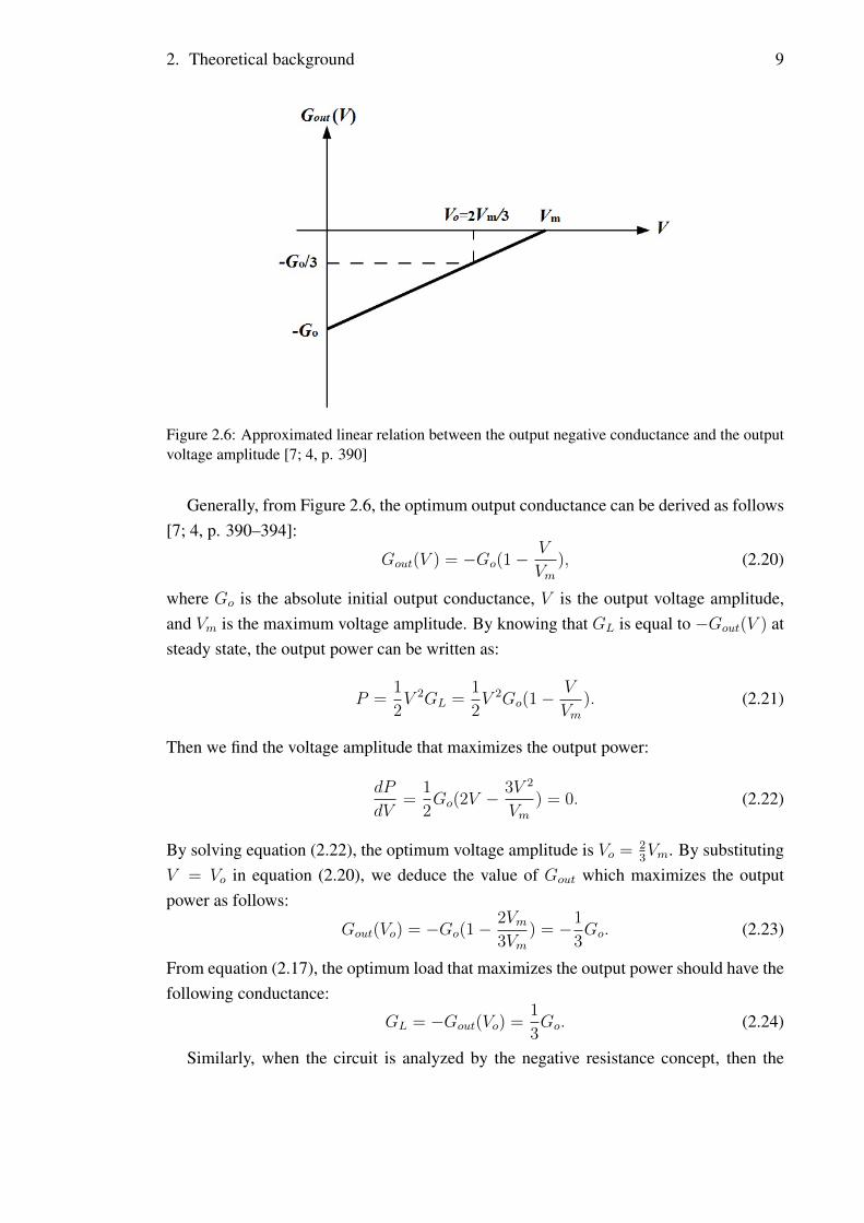
This is one of the approaches that aimed to optimize oscillators output power. Accordingto his study on the IMPATT diode oscillator [7], Gewartowski has found that the relationbetween the IMPATT diode negative conductance magnitude and the output voltage mag-nitude can be represented approximately by a straight line, as shown in Figure 2.6. And,he used this relation to prove theoretically that the maximum oscillator power is obtainedwhen the diode negative conductance magnitude is one third of its maximum initial (orstartup) value at a given biasing conditions. [7.] This approach has been widely used[2; 4, p. 390–394; 3, p. 616].
2. Theoretical background 9
Figure 2.6: Approximated linear relation between the output negative conductance and the outputvoltage amplitude [7; 4, p. 390]
Generally, from Figure 2.6, the optimum output conductance can be derived as follows[7; 4, p. 390–394]:
Gout(V ) = −Go(1−V
Vm), (2.20)
where Go is the absolute initial output conductance, V is the output voltage amplitude,and Vm is the maximum voltage amplitude. By knowing that GL is equal to −Gout(V ) atsteady state, the output power can be written as:
P =1
2V 2GL =
1
2V 2Go(1−
V
Vm). (2.21)
Then we find the voltage amplitude that maximizes the output power:
dP
dV=
1
2Go(2V −
3V 2
Vm) = 0. (2.22)
By solving equation (2.22), the optimum voltage amplitude is Vo = 23Vm. By substituting
V = Vo in equation (2.20), we deduce the value of Gout which maximizes the outputpower as follows:
Gout(Vo) = −Go(1−2Vm3Vm
) = −1
3Go. (2.23)
From equation (2.17), the optimum load that maximizes the output power should have thefollowing conductance:
GL = −Gout(Vo) =1
3Go. (2.24)
Similarly, when the circuit is analyzed by the negative resistance concept, then the

2. Theoretical background 10
output resistance, as a function of current amplitude, can be optimized as follows:
Rout(Ao) = −1
3Ro, (2.25)
where Ro is the absolute value of the initial output resistance. And the optimum loadshould have the following resistance:
RL =1
3Ro. (2.26)
2.3.2 The maximum negative resistance/conductance approach
Another approach to maximize the output power depends on the design of the feedbackelements. Maeda, followed by Grebennikov, has claimed that an optimum combination ofthe feedback elements, which maximizes the negative real part of the small-signal outputimmittance, ensures oscillations with maximum amplitude, and produces maximum outputpower. In other words, a larger initial negative resistance or conductance leads to a largeroutput amplitude and higher output power, as shown in Figure 2.7. [2; 8; 9; 10]
For instance, if the resonator and coupling reactances areX1 andX2, respectively, thentheir optimum values X0
1 and X02 that maximize Rout are the solutions of the following
equations [8]:∂Rout
∂X1
= 0, (2.27)
∂Rout
∂X2
= 0. (2.28)
Hence, the optimum output resistanceR0out and reactanceX0
out for maximum output powerare:
R0out = Rout(X
01 , X
02 ), (2.29)
X0out = Xout(X
01 , X
02 ). (2.30)
After optimizing the output impedance of the active part, we can calculate the optimumload, according to Gewartowski’s approach, as follows:
RL = −1
3R0
out, (2.31)
XL = −X0out. (2.32)
Figure 2.7 gives a graphical illustration for the main problem that this approach facesto prove its legitimacy. For a certain feedback elements combination, we assume that theblack line represents the approximated relation between the output immittance real partand output amplitude. On the one hand, if the optimum combination is placed instead,

2. Theoretical background 11
Figure 2.7: The small-signal output resistanceRout as a function of current amplitude I . The blackline shows Rout(I) based on a nonoptimal feedback design. The blue line shows where Rout(I)is supposed to shift when −Rout(0) is maximized (according to Maeda’s approach). The red lineshows another possibility that Rout(I) could be if −Rout(0) is maximized.
then this line is assumed to be shifted as the blue line according to this approach. Asa result, both oscillation amplitude and output power will increase. But on the otherhand, it has not been proven yet whether the maximum negative small-signal resistance(or conductance in other examples) provides maximum large signal negative resistance(or conductance) and, consequently, maximum amplitude of oscillation or not. So thementioned relation may also behave as the red dashed line in the same figure, providingless oscillation amplitude and less output power. In the next chapter we will deal with thisproblem, and examine the oscillator output power when Rout(0) or Gout(0) is varied onthe basis of feedback elements variation.

12
3. EVALUATION OF “MAXIMUM SMALL-SIGNALNEGATIVE RESISTANCE/CONDUCTANCE”APPROACH
This chapter is divided into two parts, computer simulations and laboratory measure-ments. In the computer simulations part, we present a systematic method, carried out ona common example of oscillator circuits, to evaluate the approach that aimed to maxi-mize the output power using the maximum negative resistance/conductance optimal de-sign. The main goal here is to compare between the oscillator output power Pout and itscorresponding output small-signal resistance/conductance (Rout(0) or Gout(0)) when os-cillator’s feedback capacitors (C1, C2, Cr) are varied. The different combinations of thefeedback capacitors can provide us with the optimal design. The resonator inductor Lr
is kept at a fixed value that provides high unloaded quality factor Q, since typically it isnot possible to vary Lr on a wide range and maintain its high Q at the same time. Themain research method was based on designing a BJT Clapp oscillator with a series res-onator, and the load was connected either in series or in parallel to the amplifier network.The negative resistance/conductance analysis was applied from the load side. Then thefeedback capacitors were varied to find out the corresponding output small-signal nega-tive resistance or conductance. Next, the optimum load value was chosen according tothe Gewartowski approach (see equations (2.24) and (2.26)), and the output power wasrecorded. Finally, the output negative small-signal resistance/conductance was comparedto the output power.
In the laboratory measurements part (section 3.2), we designed two Clapp oscillatorshaving the same configurations as in computer simulations part, where one of them wasconnected to parallel load and the other was connected to series load. For the parallel-load circuit, two feedback combinations were tested, one that supposed to deliver themaximum output power, and the other one that supposed to have the maximum nega-tive conductance (according to simulation results). Then we compared between the twocombinations regarding the measured output power. For the series-load circuit, we didthe same, but in addition, we plotted the whole output power curve as a function of thefeedback capacitors. Then we extracted from this curve, the previously mentioned twocombinations and compared between them.

3. Evaluation of “maximum small-signal negative resistance/conductance” approach 13
3.1 Computer simulations
Two oscillator circuits were designed and simulated by “Advanced Design System (ADS)2009” from Agilent Technologies [16]. The first one is connected to a parallel orientedload, where the load is directly in parallel to the amplifier output port. Figure 3.1 showsthe placement of the load with respect to both amplifier and feedback networks. The samecircuit can be redrawn in more simplified way, as shown in Figure 3.2. The second circuitis connected to a series oriented load, where the load is connected between the amplifieroutput positive terminal and the feedback input positive terminal, as shown in Figure 3.3and Figure 3.4.
Figure 3.1: A common emitter BJT Clapp oscillator having a π-type feedback network, and con-nected to a parallel load. The load is connected between transistor collector and emitter nodes.Biasing circuit is omitted.
Figure 3.2: Same oscillator circuit as in Figure 3.1, but the components were rearranged in a moresimple way, and the collector node is grounded. Output conductance Gout is shown.

3. Evaluation of “maximum small-signal negative resistance/conductance” approach 14
Figure 3.3: A common emitter BJT Clapp oscillator having a π-type feedback network, and con-nected to a series load. Biasing circuit is omitted.
Figure 3.4: Same oscillator circuit as in Figure 3.3, but the components were rearranged in a moresimple way, the emitter node is grounded. Output resistance Rout is shown.
For each of the two circuits, one procedure was performed to find Pout and the corre-spondingGout(0) orRout(0) for every change of the feedback elements capacitors. Duringthis procedure, the oscillation frequency was kept constant at 100.0 ± 0.5 MHz by meansof properly adjusting values of Cr, and |Gout(0)|/GL (or |Rout(0)|/RL) ratio was keptconstant at its optimal value (3.0 ± 0.1). The following flow chart shown in Figure 3.5summarizes the whole simulation procedure.

3. Evaluation of “maximum small-signal negative resistance/conductance” approach 15
-Start procedure-Select “x” from
4, 2, 1, 0.5, 0.25
Select initial value of RL
Select C'1
Select Cr
Run HB simulation
Is there an oscillation at
100.0±0.5 MHz?
- Record fo and Pout.- Run S-parameters simulation
at fo.- Record Gout (or Rout).- Calculate -Gout/GL (or
-Rout/RL).
Yes
Is -Gout/GL (or -Rout/RL)
equal to 3.0±0.1?
Calculate the needed RL which
fulfills:
GL= -(1/3) Gout (or RL= -(1/3) Rout)
No
No
- Record fo, Pout, Gout
(or Rout), -Gout/GL (or -Rout/RL)
- End simulation for this C'1
Is there another C'1Within the oscillation
range ?
No
Yes
Yes
Figure 3.5: The simulation procedure for the 100 MHz Clapp oscillator to obtain Pout and Gout
(or Rout). This chart is for both load orientations (parallel and series), where x = C ′1/C′2.
3.1.1 Parallel load circuit
The simulated Clapp oscillator schematic circuit is shown in Figure 3.6. Its invertingamplifier network consisted of a common emitter NPN BJT from “MPS918” type [12].This BJT was biased at a collector-emitter voltage VCE = 5 V and a collector current IC =
20 mA, using a biasing circuit consisted of two resistancesR1 = 15.04 kΩ andR2 = 4.96
kΩ of total 20 kΩ. The load RL was connected between collector and emitter. Theoscillator’s feedback network was a π-type network, and consisted of a series resonator

3. Evaluation of “maximum small-signal negative resistance/conductance” approach 16
and a phase shifter. The resonator was formed by a resonator inductor Lr connected inseries to a resonator (tuning) capacitor Cr. The resonator inductor was kept constant1 at500 nH, while Cr was slightly varied2 to tune for 100.0 ± 0.5 MHz oscillation frequency.The phase shifter consisted of two coupling capacitors C1 and C2, to provide a positivefeedback, or in other words, to provide basically the other 180 phase shift so that thetotal loop phase shift is zero or 360 . For simplicity, the relation between the couplingcapacitances was defined by the ratio x = C ′1/C
′2, where C ′1 and C ′2 were defined as:
C ′1 = C1 + Cbe, (3.1)
C ′2 = C2 + Cce, (3.2)
where Cbe and Cce are the base-emitter and collector-emitter capacitances,3 respectively.
Figure 3.6: Clapp oscillator schematic circuit connected to parallel load (biasing circuit is in-cluded). A “harmonic balance” simulation was carried out to test fo and Pout. Then an “S-parameters” simulation was carried out to test Gout(0). The current components’ values deliverthe maximum output power for x = 4 (See “Appendix A”: Table A.1 at C ′1 = 26 pF).
For each value of x, the capacitance C ′1 was varied within the range of 8 to 200 pF witha suitable steps. At every value of C ′1, three consequent simulation steps were performed.First, a “harmonic balance” simulation was done for the circuit shown in Figure 3.6 toadjust the oscillation frequency at 100.0 ± 0.5 MHz4 by selecting a suitable Cr value.While an “initial” load was connected, for the fact that the load has no significant effect
1At low Values of C ′1 and C ′
2, the resonator inductor value exceeded 500 nH to maintain oscillationfrequency at 100 MHz.
2At low Values of C ′1 and C ′
2, the resonator capacitor was increased significantly to keep the oscillationfrequency at 100 MHz. Thus, the oscillator in this case was considered a Colpitts oscillator.
3During simulations, the capacitanceCbe was assumed to be equal to 7.7 pF [11], whileCce was ignored.4See “Appendix A” for frequency values.

3. Evaluation of “maximum small-signal negative resistance/conductance” approach 17
on the frequency. We take here an example from “Appendix A” tables for C ′1 = 26 pF andx = 4 for more clarification. The harmonic balance simulation was run with an initialload of 90 Ω, while Cr was slightly varied until it reached 5.9 pF, which produces anoscillation at fo = 99.7 MHz. Thus the frequency was adjusted, and we did not have torecord the output power value that obtained from this step.
In the second step, the one port small-signal negative conductance analysis was ap-plied, where an “S-parameters” simulation was run to record the small-signal output neg-ative conductance for the same circuit, after assigning the value ofCr. The circuit configu-ration in Figure 3.6 was the same except that the load was replaced by a 50-Ω termination.In our example, the tested negative conductance was−32.03 mS. Then, the optimum loadwas calculated according to equation (2.24), and it was 3/(32.03 mS) ≈ 93.66Ω. Thethird and last step was a repetition of the first one, but with connecting the optimum loadcalculated in the second step. The goal was to test the oscillator output power. For ourexample, the fundamental component of the output power was recorded (18.189 dBm)along with the oscillation frequency (99.8 MHz).
Figure 3.7: An example of the simulated output power spectrum results from the harmonic balancesimulation, for C ′1 = 26 pF and RLopt. = 95 Ω.
Notice that the optimum load was different from the initial load and leads to a slightdeviation in frequency (0.1 MHz) between the first and last step. Therefore, these stepsmight be repeated until we reach a constant frequency through all the procedure. Aftertwo more iterations, more accurate results have been obtained; the final optimum loadwas 95 Ω, which delivers 18.206 dBm at 99.9 MHz, as shown in Figure 3.7. WhileGout(0) was −31.51 mS and |Gout(0)|/GL = 2.99. By the end of these three steps

3. Evaluation of “maximum small-signal negative resistance/conductance” approach 18
we have obtained one point (Gout(C′1), Pout(C
′1)) corresponding to a certain value of C ′1.
The whole procedure was repeated for all C ′1 values within the specified range. Then, adifferent x value was selected and the same work was done for x = 4, 2, 1, 1/2, and 1/4.
3.1.2 Series load circuit
For the Clapp oscillator configuration having a series oriented load, we tried first to an-alyze the circuit using the negative conductance concept, but we could not attain anyoscillation at the output if we connect a load having GL = −1
3Gout(0). Therefore, we
have applied the negative resistance analysis for this circuit. So the same procedure asin the previous section was done except that the small-signal initial output resistance wastested instead. Figure 3.8 shows the schematic circuit used for “harmonic balance” simu-lation. The same circuit is also used for “S-parameters” simulation by replacing the loadby a 50-Ω termination. The biasing circuit was having R1 = 15.29 kΩ, R2 = 4.71 kΩ,and a DC source VDC = 5.2 V. This biasing circuit ensured the same quiescent point.
Figure 3.8: Clapp oscillator schematic circuit connected to series load (biasing circuit is included).A “harmonic balance” simulation was carried out to test fo and Pout. Then an “S-parameters”simulation was carried out to testRout(0). Output voltage is Vout = Vout1−Vout2. See “AppendixB”: Table B.2, for the choices of C ′1 and RL, and the corresponding results.
3.1.3 Results and discussion
For the Clapp oscillator configuration having a parallel oriented load, numerical resultsare given in “Appendix A”, and plotted by Matlab as shown in Figure 3.9. From this figure
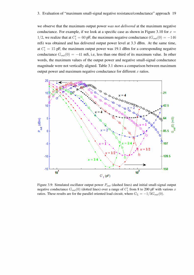
3. Evaluation of “maximum small-signal negative resistance/conductance” approach 19
we observe that the maximum output power was not delivered at the maximum negativeconductance. For example, if we look at a specific case as shown in Figure 3.10 for x =
1/2, we realize that at C ′1 = 60 pF, the maximum negative conductance (Gout(0) = −146
mS) was obtained and has delivered output power level at 3.3 dBm. At the same time,at C ′1 = 15 pF, the maximum output power was 19.1 dBm for a corresponding negativeconductance Gout(0) = −41 mS, i.e, less than one third of its maximum value. In otherwords, the maximum values of the output power and negative small-signal conductancemagnitude were not vertically aligned. Table 3.1 shows a comparison between maximumoutput power and maximum negative conductance for different x ratios.
Figure 3.9: Simulated oscillator output power Pout (dashed lines) and initial small-signal outputnegative conductance Gout(0) (dotted lines) over a range of C ′1 from 8 to 200 pF with various xratios. These results are for the parallel oriented load circuit, where GL = −1/3Gout(0).

3. Evaluation of “maximum small-signal negative resistance/conductance” approach 20
Figure 3.10: Simulated comparison between two C ′1 values at x = 0.5: for C ′1 = 15 pF oneobtains maximum output power while for 60 pF one obtains maximum negative conductance. C ′1is varied from 8 to 105 pF.
Table 3.1: Comparison between two C ′1 values (for every x): one gives maximum Pout, while theother one gives maximum negative Gout, for oscillator with parallel load.
x C′1 (pF) Gout(0) (mS) Pout (dBm)
426 -32 18.2
75 -64 11.3
222 -39 18.7
80 -96 8.1
120 -50 19.5
75 -127 5.3
0.515 -41 19.1
60 -146 3.3
0.2511 -26 16.8
45 -147 0.8

3. Evaluation of “maximum small-signal negative resistance/conductance” approach 21
For plotting Gout as a function of the voltage amplitude, first we presume that theirrelation is represented by a straight line according to [7], and hence can be defined bytwo points. The first point is (Gout(0), 0), and the second point is (0, Vm). Where Vm wascalculated as follows:
Pout =1
2
V 2
RL
=1
2
(2/3Vm)2
RL
, (3.3)
Vm =3√2
√PoutRL. (3.4)
The resultant Gout(V ) lines at x = 4 and 2 are shown in Figures 3.11 and 3.12, respec-tively. The lines illustrate the same simulation results from another perspective. In thesefigures, The red line which has maximum |Gout(0)| is not leading to maximum Vm whileGout magnitude is diminishing. Whereas the blue line delivers the maximum output powerat its steady-state point (at V = 2
3Vm) despite of having less |Gout(0)|. While green lines
were resulted from other feedback combinations. More graphs for the remaining x ratiosare shown in “Appendix C”.
Figure 3.11: Simulation results for the small-signal output conductance Gout as a function ofV with x = 4. a) Blue line: maximum power combination. b) Red line: maximum negativeconductance combination. c) Green lines: other combinations.

3. Evaluation of “maximum small-signal negative resistance/conductance” approach 22
Figure 3.12: Simulation results for the small-signal output conductance Gout as a function ofV with x = 2. a) Blue line: maximum power combination. b) Red line: maximum negativeconductance combination. c) Green lines: other combinations.
For the Clapp oscillator configuration having a series oriented load, results are recordedin “Appendix B” and were plotted for x = 4, 2, 1, and 0.55, as shown in Figure 3.13.Similarly we observe that the maximum output power was not delivered at the maximumnegative resistance. For example, Figure 3.14 shows a specific case at x = 2, wherewe notice that at C ′1 = 45 pF, the maximum negative resistance Rout(0) = −1.46 kΩ
was achieved, and has delivered output power level at 10.2 dBm. On the other hand, atC ′1 = 123 pF, the output power has reached the maximum at 16.5 dBm for a correspondingnegative resistance Rout(0) = −368 Ω. Table 3.2 shows a comparison between maximumoutput power and maximum negative resistance for different x ratios.
5Curve x = 1/4 could not be plotted because the condition RL = −1/3Rout(0) did not hold for loadswithin oscillation range.

3. Evaluation of “maximum small-signal negative resistance/conductance” approach 23
Figure 3.13: Simulated oscillator output power Pout (dashed lines) and initial small-signal outputnegative resistance Rout(0) (dotted lines) over a range of C ′1 from 15 to 200 pF with various xratios. These results are for the series oriented load circuit, where RL = −1/3Rout(0).
Figure 3.14: Simulated comparison between twoC ′1 values: forC ′1 = 45 pF one obtains maximumnegative resistance while for 123 pF one obtains maximum output power. C ′1 is from 30 to 200 pF.

3. Evaluation of “maximum small-signal negative resistance/conductance” approach 24
Table 3.2: Comparison between two C ′1 values (for every x): one gives maximum Pout, while theother one gives maximum negative Rout, for oscillator with series load.
x C′1 (pF) Rout(0)(Ω) Pout (dBm)
415 -9445 3.0
175 -365 16.1
245 -1460 10.2
123 -368 16.5
170 -384 16.0
81 -333 16.7
0.545 -76 15.1
60 -138 13.3
The output resistance Rout also can be plotted as a function of the current amplitude Iconsidering a straight line relation defined by two points. The first point is (Rout(0), 0),and the second point is (0, Im). Where Im was calculated as follows:
Pout =1
2I2RL =
1
2(2
3Im)2RL, (3.5)
Im =3√2
√Pout
RL
. (3.6)
Results of Rout(I) lines at x = 4 and 2 are shown in Figures 3.15 and 3.16. The red linewhich has maximum |Rout(0)| is not leading to maximum Vm while Rout magnitude isdiminishing. The blue line delivers the maximum output power at its steady-state point(atA = 2
3Am) although it has much less |Rout(0)|. More graphs for the remaining x ratios
are shown in “Appendix D”.

3. Evaluation of “maximum small-signal negative resistance/conductance” approach 25
Figure 3.15: Simulation results for the small-signal output resistance Rout as a function of I withx = 4. a) Blue line: maximum power combination. b) Red line: maximum negative resistancecombination. c) Green lines: other combinations.
Figure 3.16: Simulation results for the small-signal output resistance Rout as a function of I withx = 2. a) Blue line: maximum power combination. b) Red line: maximum negative resistancecombination. c) Green lines: other combinations.

3. Evaluation of “maximum small-signal negative resistance/conductance” approach 26
The results show a significant disagreement with the approach - under examination -which aimed to maximize oscillator output power. So, maximizing negative small-signalresistance or conductance at the output port of the active part does not guarantee deliv-ery of maximum output power. Another observation from the results is that the parallelconnected loads deliver more output power than the series ones if the feedback elementsare freely selected. Figure 3.17 illustrates a comparison between parallel and series loadconnections. It is shown that parallel connection gives 18.7 and 18.2 dBm, while the se-ries one gives 16.5 and 16.1 dBm as peak powers, for x = 2 and 4, respectively. Also, wenotice that the parallel load delivers more power at lower C ′1 and C ′2 values, whereas theseries load delivers more power at higher C ′1 and C ′2 values.
Figure 3.17: Simulated comparison of Output power results of parallel and series oriented loadoscillators for x = 2 (blue curves) and x = 4 (red curves).
3.2 Laboratory measurements
This section is a continuation to the work done in section 3.1. We aim to verify practicallythe results obtained by simulations. The following laboratory measurements were doneusing a spectrum analyzer of model “E4407B” from Agilent technologies [17]. The spec-trum analyzer was set to a Resolution Bandwidth (RBW) of 300 kHz, Video Bandwidth

3. Evaluation of “maximum small-signal negative resistance/conductance” approach 27
(VBW) of 300 kHz and Reference level equal to 15 dBm. An input DC voltage sourcewas used along with a series ammeter for transistor biasing.
3.2.1 Parallel load circuit
An oscillator circuit was designed, as per the schematic shown in Figure 3.6, on a printedcircuit board (PCB) to perform a power measurement test for two feedback elementscombinations. The first combination was the one that delivered the maximum outputpower. The second one was by which the maximum conductance has occurred. The loadwas connected in parallel and the coupling ratio xwas equal to two. The two combinations- under test - were as follows:
• The maximum output power combination6: C ′1 = 21 pF, C ′2 = 10.5 pF, Cr = 5.6
pF, Lr = 500 nH, and RL = 83 Ω.
• The maximum negative conductance combination: C ′1 = 80 pF, C ′2 = 40 pF, Cr =
3.4 pF, Lr = 500 nH, and RL = 31 Ω.
The final PCB design is shown in Figure 3.18. Transistor model was “PN3563” whichhas similar characteristics to “MPS918” [13]. The resonator inductor was formed by anair wounded copper coil, and its specifications is given in “Appendix E”. The remainingcircuit components are illustrated in Table 3.3. A 5-V DC source, along with a seriesammeter, was connected between the collector node and ground, while the 20-kΩ poten-tiometer was varied to draw a DC current ICC = 20.2 mA, which ensures a collectorcurrent IC = 20 mA (see “Appendix F” for biasing settings). The output power wasmeasured by the spectrum analyzer.
Figure 3.18: The final Clapp oscillator circuit design on a PCB.
6This combination provided the second maximum output power on “x = 2” curve with Pout = 18.6dBm, while the maximum power was 18.7 dBm. It was chosen because their elements’ values have thenearest match to the standard components’ values in the laboratory.

3. Evaluation of “maximum small-signal negative resistance/conductance” approach 28
Table 3.3: Components discription for the PCB circuit.
Component Specification
Transistor PN3563 model
Biasing RF choke 2.2 µH
Output RF choke 2.2 µH
Source DC Block 330 pF
Output DC Block 390 pF
Potentiometer 20 kΩ
RF connector SMA type
Capacitors Disc Ceramic type
To test the circuit with the maximum power combination, it was difficult to use thesimulated capacitor values through the practical test due to the limitation of capacitorsstandard values in the laboratory. However, the values chosen for test were as close aspossible to the simulated ones. So the final values for the combination - under test - was:
• C ′17 = 19.7 pF, C ′2 = 10 pF, Cr = 5.6 pF, Lr = 500 nH, and RL = 83.3 Ω.
Based on the simulations, this combination has Gout(0) = −33 mS. The Load RL wasformed by a series connection of the spectrum analyzer internal resistance (50 Ω) and anexternal resistor of 33.3 Ω as shown in Figure 3.19.
Test results are illustrated in Figure 3.20, that shows the fundamental and two har-monics components for the spectrum analyzer input power PS.A.. From this figure, themeasured value of PS.A. was 11.96 dBm at 100.3 MHz. By the following calculations, theoutput power was deduced:
PS.A. =1
2
V 2S.A.
RS.A.
, (3.7)
VS.A. =√
2PS.A.RS.A. (3.8)
=
√(2)
(101.196
1000
)(50)
= 1.253 V,
VS.A =RS.A
RS.A +Rex.
Vout, (3.9)
7The ceramic capacitor used was C1 = 12 pF, assuming Cbe = 7.7 pF.

3. Evaluation of “maximum small-signal negative resistance/conductance” approach 29
Figure 3.19: Oscillator schematic showing the load formation and connection for the maximumpower combination. Biasing circuit is omitted.
Vout =RS.A +Rex.
RS.A
VS.A (3.10)
=
(50 + 33.3
50
)(1.253)
= 2.088 V,
Pout =1
2
V 2out
RL
=1
2
(2.0882
83.3
)= 26.2 mW = 14.18 dBm. (3.11)
From equation (3.11), the output (or load) power was equal to 14.18 dBm (26.2 mW).Next, we will repeat the same work done using the maximum negative conductance com-bination.
3. Evaluation of “maximum small-signal negative resistance/conductance” approach 30
Figure 3.20: Spectrum analyzer screenshot showing the output power for the maximum powercombination.
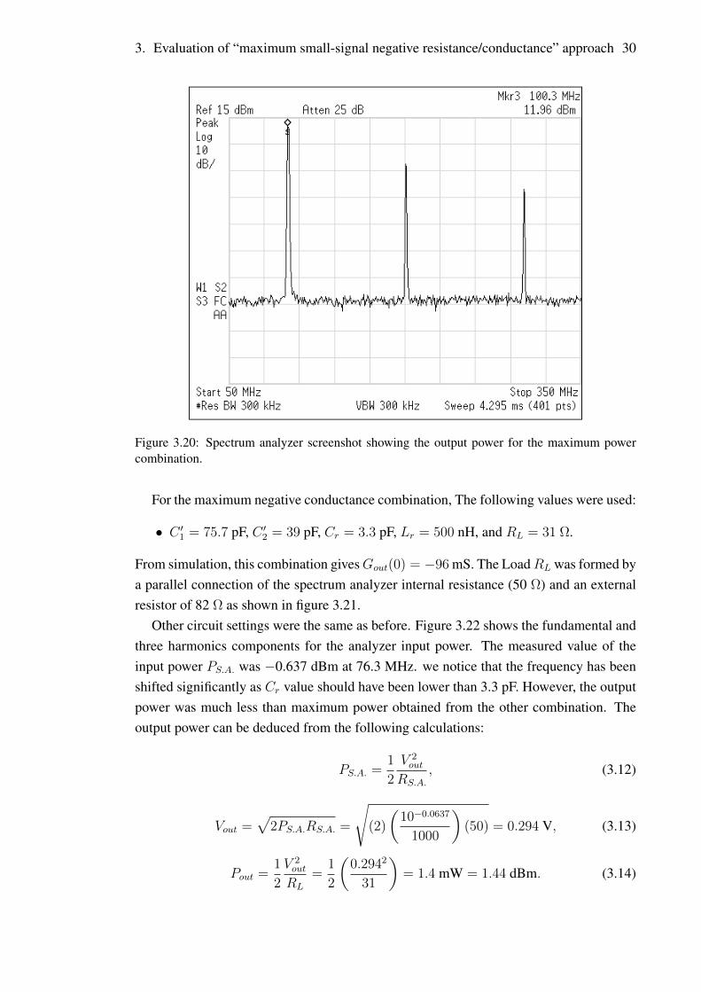
For the maximum negative conductance combination, The following values were used:
• C ′1 = 75.7 pF, C ′2 = 39 pF, Cr = 3.3 pF, Lr = 500 nH, and RL = 31 Ω.
From simulation, this combination givesGout(0) = −96 mS. The LoadRL was formed bya parallel connection of the spectrum analyzer internal resistance (50 Ω) and an externalresistor of 82 Ω as shown in figure 3.21.
Other circuit settings were the same as before. Figure 3.22 shows the fundamental andthree harmonics components for the analyzer input power. The measured value of theinput power PS.A. was −0.637 dBm at 76.3 MHz. we notice that the frequency has beenshifted significantly as Cr value should have been lower than 3.3 pF. However, the outputpower was much less than maximum power obtained from the other combination. Theoutput power can be deduced from the following calculations:
PS.A. =1
2
V 2out
RS.A.
, (3.12)
Vout =√
2PS.A.RS.A. =
√(2)
(10−0.0637
1000
)(50) = 0.294 V, (3.13)
Pout =1
2
V 2out
RL
=1
2
(0.2942
31
)= 1.4 mW = 1.44 dBm. (3.14)

3. Evaluation of “maximum small-signal negative resistance/conductance” approach 31
Figure 3.21: Oscillator schematic showing the load formation and connection for the maximumnegative conductance combination. Biasing circuit is omitted.
Figure 3.22: Spectrum analyzer screenshot showing the output power for the maximum conduc-tance combination.

3. Evaluation of “maximum small-signal negative resistance/conductance” approach 32
From the last equation, the output power was 1.44 dBm, which is much lower than themaximum output power (14.2 dBm) despite having a maximum negative conductance inthis case. All in all, the maximum power combination has practically delivered higherpower than the power delivered by the maximum conductance combination (either thesimulated or the laboratory tested one). Table 3.4 summarizes the main results of thissection.
Table 3.4: Comparison between simulation and laboratory results for the output power of oscillatorwith parallel load, at x = 2.
Pout (dBm)
Simulation results
Maximum Pout
combination 18.7
Maximum Gout
combination 8.1
Laboratory results
Maximum Pout
combination 14.2
Maximum Gout
combination 1.4
3.2.2 Series load circuit
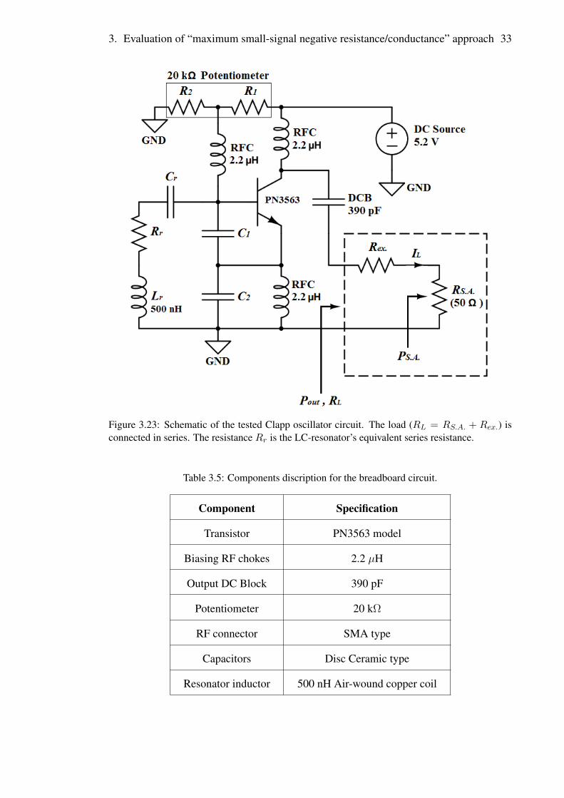
This is the second part of the laboratory measurements, where we have tested the oscillatorcircuit that is connected to a series load. Figure 3.23 shows the schematic of the testedcircuit, while table 3.5 shows more details about the used components. A 5.2-V DCsource was connected along with a series ammeter which was adjusted to read 20.3 mAon its screen using a 20-kΩ potentiometer. Therefore, the quiescent point remained thesame at VCEQ = 5 V and ICQ = 20 mA (see “Appendix F” for biasing settings). The finalcircuit was built on a solderless breadboard as shown in Figure 3.24.
3. Evaluation of “maximum small-signal negative resistance/conductance” approach 33
Figure 3.23: Schematic of the tested Clapp oscillator circuit. The load (RL = RS.A. + Rex.) isconnected in series. The resistance Rr is the LC-resonator’s equivalent series resistance.
Table 3.5: Components discription for the breadboard circuit.
Component Specification
Transistor PN3563 model
Biasing RF chokes 2.2 µH
Output DC Block 390 pF
Potentiometer 20 kΩ
RF connector SMA type
Capacitors Disc Ceramic type
Resonator inductor 500 nH Air-wound copper coil

3. Evaluation of “maximum small-signal negative resistance/conductance” approach 34
Figure 3.24: The final 70 MHz Clapp oscillator circuit design on a breadboard.
The oscillation frequency was set to 70 MHz instead of 100 MHz, because the testedcircuit could not produce oscillations with Cr less than 10 pF. Figure 3.25 shows thesimulated circuit with two Cr choices, where at Cr = 3.3 pF, the circuit oscillates around100 MHz. While at Cr = 10 pF, the circuit oscillates around 70 MHz. As a result, thesimulations done in section 3.1.2 were repeated for one curve only (x = 2) at 70± 1 MHzto support the Lab. measurements. The new simulation results at 70 MHz are plotted inFigure 3.26 (see “Appendix B” for the recorded numerical results). From this figure, weobserve that the maximum output power (16.5 dBm) was delivered at a local negativeresistance value Rout(0) = −402 Ω, so the same outcomes illustrated in section 3.1 wereobtained at a different frequency.
Figure 3.25: Simulation results for fo over a range of C ′1 values at Cr3.3 and 10 pF. The Clapposcillator is connected to a series 50 Ω load, while x = 2.

3. Evaluation of “maximum small-signal negative resistance/conductance” approach 35
Figure 3.26: Simulation results at 70 MHz. Pout (dashed lines) and Rout(0) (dotted lines) overa range of C ′1 from 30 to 340 pF at x = 2. These results are for the series oriented load circuit,where RL = 1
3Rout(0).
For the breadboard circuit test, x was set to two as close as possible, and the load wasvaried for each C ′1 value to examine the effect of load variation. The spectrum analyzerinput power was measured as in Figure 3.27. With the help of Figure 3.23, the outputpower was calculated by the following steps:
PS.A. =1
2I2LRS.A., (3.15)
Once the spectrum analyzer input power PS.A. is measured, the load (output) current iscalculated as follows:
IL =
√2PS.A.
RS.A.
=
√2PS.A.
50, (3.16)

3. Evaluation of “maximum small-signal negative resistance/conductance” approach 36
and the output power is obtained from:
Pout =1
2I2LRL
=1
2I2L(Rex. + 50). (3.17)
Figure 3.27: Spectrum analyzer screenshot for PS.A with the optimum feedback combination(C ′1 = 64 pF, C2 = 33 pF and Cr = 12 pF). The fundamental and six harmonic components areshown.
The measured output power was plotted against load for differentC ′1 values, and resultsare shown in Figure 3.28, where we can see that the power response as a function of loadvariation is nearly the same for all C ′1 values. The highest output powers were deliveredfor load range of 118 to 201 Ω (for all C ′1 values). The maximum output power was 17.1dBm, and was delivered at C ′1 = 76 pF and RL = 132 Ω. So the highest efficiency wasnearly 50%. Measurement results are recorded in “Appendix G”.

3. Evaluation of “maximum small-signal negative resistance/conductance” approach 37
Figure 3.28: Laboratory test results for the output power as a function of load at different C ′1values. The oscillation frequency fo = 70 MHz.
The measured maximum output power was plotted as a function of C ′1 in Figure3.29, and also the corresponding Rout(0) was simulated by ADS and plotted in the samegraph. From this figure we observe that the maximum output power was delivered atRout(0) = −1.482 kΩ, which is not the maximum negative resistance. Hence, this prac-tical experiment also confirms the main outcome. Table 3.6 summarizes the main resultsof this section.

3. Evaluation of “maximum small-signal negative resistance/conductance” approach 38
Figure 3.29: Laboratory test results at 70 MHz for the optimum output power as a function of C ′1.The simulated Rout(0) curve is also shown.
Table 3.6: Comparison between simulation and laboratory results for the output power of oscillatorwith series load, at x = 2 and fo = 70 MHz.
Pout (dBm)
Simulation results
Maximum Pout
combination 16.5
Maximum Rout
combination 9.9
Laboratory results
Maximum Pout
combination 17.1
Maximum Rout
combination 10.2

39
4. CONCLUSION
BJT Clapp oscillators with series resonator were designed and analyzed using the nega-tive resistance concept. And they were connected to the load by two possible orientations,parallel and series to the amplifier output port. The feedback elements’ reactances werevaried while the load was maintained at its supposedly optimal value for maximum out-put power. The oscillator output power was tested against the negative real part of thesmall-signal output immittance at startup (i.e, when the oscillation amplitude is nearlyzero and begins to rise). The results have shown a significant disapproval with the exist-ing approach that aimed to maximize the output power through maximizing the negativeresistance or conductance. In this experiment, the maximum output power was deliv-ered at less than half of the maximum startup negative resistance/conductance. Therefore,results have revealed the deficiency of this approach as one of the current methods forimplementing optimum power oscillators. Although this approach was first published in1975 by Maeda, it is still the basis of state-of-the-art analytical methods, as we can learnfrom Grebennikov’s recently published book in 2007 [18].
The design examples revealed also some other interesting results. The load orientation,whether parellel- or series-connected, can make a difference in output power. Accordingto the simulations performed in this thesis, the output power was generally higher toparallel-connected loads than to series-connected loads. Also a difference was observedin optimal coupling capacitances. Capacitances that provided maximum output powerwere generally lower for the parallel-loads than for the series-loads. This may have somepractical implications as what comes to the availability of or preferences for larger orsmaller capacitances.
The methods used in this thesis can be applied for other configurations of RF or mi-crowave oscillators to assess the approach under examination. Clearly, further researchis recommended to be carried out to invent new methods that can provide more precisebasis for maximizing the output power. Some of this research should focus on studyingin-depth, analytically or by computer aided design tools, the negative resistance curves interms of output oscillation amplitude.

40
REFERENCES
[1] J. K. Clapp. An inductance-capacitance oscillator of unusual frequency stability.Proc. IRE 36(1948)3, pp. 356–358.
[2] M. Maeda, K. Kimura, and H. Kodera. Design and Performance of X-Band Oscilla-tors with GaAs Schottky-Gate Field-Effect Transistors. IEEE Trans. Microw. TheoryTech. 23(1975)8, pp. 661–667. (1975).
[3] D. M. Pozar. Microwave engineering. 4th ed. New Jersey 2011, Wiley. 732 p.
[4] G. Gonzalez. Microwave transistor amplifiers analysis and design. 2nd ed. New Jer-sey 1996, Prentice-Hall. 506 p.
[5] R. Ludwig and P. Bretchko. RF circuit design theory and applications. New Jersey2000, Prentice-Hall. 642 p.
[6] R. W. Rhea. Oscillator design and computer simulation. 2nd ed. Georgia 1995, No-ble. 320 p.
[7] J. Gewartowski. The effect of series resistance on avalanche diode (IMPATT) oscil-lator efficiency. Proc. IEEE 56(1968)6, pp. 1139–1140.
[8] A. V. Grebennikov and V. V. Nikiforov. An analytic method of microwave transistoroscillator design. Int. J. Electronics 83(1997)6, pp. 849–858.
[9] A. V. Grebennikov. A simple analytic method for transistor oscillator design. Ap-plied Microwave and Wireless 12(2000)1, pp. 36–44.
[10] A. V. Grebennikov. Microwave transistor oscillators: an analytic approach to sim-plify computer-aided design. Microwave J. [electronic journal]. (1999), [accessedon 22.03.2013]. Available at: http://www.microwavejournal.com/articles/2640.
[11] O. Lunden, K. Konttinen and M. Hasani. A simple technique for oscillator powercalculation. Tampere 2012. To be published.
[12] On Semiconductor. (2013, April 7). MPS918, MPS3563 amplifier transistorsdata sheet [online]. Available at: http://www.datasheetcatalog.org/datasheet/on_semiconductor/MPS918-D.PDF.
[13] Fairchild Semiconductor. (2013, April 7). PN3563 data sheet [online]. Available at:http://www.foxdelta.com/products/freqcounter/fc3-sk/PN3563.pdf.
[14] J. R. Vig. Quartz crystal resonators and oscillators for frequency control and timingapplications- a tutorial. New Jersey 1997, U.S. Army Communications-ElectronicsCommand, SLCET-TR-88-1 (Rev. 8.0). 287 p.
REFERENCES 41
[15] R. Ludwig and G. Bogdanov. RF circuit design theory and applications. 2nd ed. NewJersey 2000, Prentice-Hall. 720 p.
[16] Agilent Technologies. (2013, May 8). ADS 2009 product release [online]. Availableat: http://www.home.agilent.com/agilent/product.jspx?nid=-34346.870777.00&lc=eng&cc=GB.
[17] Agilent Technologies. (2013, May 10). E4407B ESA-E Spec-trum Analyzer, 9 kHz to 26.5 GHz [online]. Available at: http://www.home.agilent.com/en/pd-1000002791%3Aepsg%3Apro-pn-E4407B/esa-e-spectrum-analyzer-100-hz-to-265-ghz.
[18] A. Grebennikov. RF and microwave transistor oscillator design. Wiley, 2007.

42
APPENDIX A. SIMULATION RESULTS FOR 100MHZ CLAPP OSCILLATOR CONNECTED TOPARALLEL LOAD
Table A.1: Simulation results for 100 MHz oscillator with parallel load with x = 4 and(−Gout/GL) = 3.0± 0.1.
C′1 Cr Lr RL fo Gout(0) (−Gout(0)/GL) Pout Vm
(pF) (pF) (nH) (Ω) (MHz) (mS) (dBm) (V)
151 50 6002 373 99.98 -8.04 3.00 14.787 7.109
16 16 6002 304 99.7 -9.87 3.00 15.395 6.883
18 33 500 207 100.4 -14.47 3.00 16.396 6.374
20 13 500 162 100.0 -18.49 3.00 17.048 6.078
21 9.7 500 145 100.4 -20.69 3.00 17.369 5.967
22 8.2 500 132 100.5 -22.75 3.00 17.628 5.865
23 7.3 500 120 100.4 -24.9 2.99 17.858 5.742
24 6.6 500 111 100.5 -26.91 2.99 18.006 5.618
25 6.2 500 103 100.2 -29.16 3.00 18.126 5.487
26 5.9 500 95 99.9 -31.51 2.99 18.206 5.318
27 5.7 500 90 99.6 -33.44 3.01 17.991 5.050
28 5.2 500 85 100.4 -35.18 2.99 17.632 4.709
29 5.2 500 81 99.7 -37.26 3.02 17.364 4.457
1Combinations for lower C ′1 values, in this table and the subsequent tables, with same fo, x and
−Gout/GL values could not be simulated.2Higher Lr values used, in this table and in the subsequent tables, to keep the frequency at 100 MHz
approximately.

APPENDIX A. 43
Table A.2: Simulation results for 100 MHz oscillator with parallel load with x = 4 and(−Gout/GL) = 3.0± 0.1 (continued).
C′1 Cr Lr RL fo Gout(0) (−Gout(0)/GL) Pout Vm
(pF) (pF) (nH) (Ω) (MHz) (mS) (dBm) (V)
30 5 500 77 99.8 -39.09 3.01 17.043 4.188
35 4.5 500 64 99.5 -47.05 3.01 15.765 3.296
40 4.2 500 57 99.5 -52.92 3.02 14.771 2.774
45 3.9 500 53 100.3 -56.41 2.99 13.927 2.427
50 3.9 500 50 99.5 -59.77 2.99 13.260 2.183
55 3.8 500 49 99.6 -61.29 3.00 12.787 2.047
60 3.7 500 48 99.8 -62.41 3.00 12.304 1.916
65 3.7 500 48 99.5 -62.94 3.02 12.025 1.856
70 3.6 500 48 99.9 -62.98 3.02 11.677 1.783
75 3.6 500 47 99.6 -63.68 2.99 11.284 1.686
80 3.5 500 48 100.1 -62.66 3.01 11.046 1.658
85 3.5 500 48 99.9 -62.93 3.02 10.772 1.606
90 3.5 500 48 99.7 -62.92 3.02 10.498 1.556
95 3.5 500 48 99.5 -62.8 3.01 10.224 1.508
100 3.4 500 48 100.1 -62.37 2.99 9.832 1.442
110 3.4 500 49 99.8 -61.19 3.00 9.361 1.380
120 3.4 500 50 99.6 -60.1 3.01 8.876 1.318
130 3.3 500 51 100.2 -59.26 3.02 8.219 1.234
140 3.3 500 54 100.1 -55.85 3.02 7.824 1.213
150 3.3 500 55 99.9 -54.62 3.00 7.288 1.151
160 3.3 500 57 99.8 -52.92 3.02 6.786 1.106
170 3.3 500 59 99.7 -51.23 3.02 6.261 1.060

APPENDIX A. 44
Table A.3: Simulation results for 100 MHz oscillator with parallel load with x = 4 and(−Gout/GL) = 3.0± 0.1 (continued).
C′1 Cr Lr RL fo Gout(0) (−Gout(0)/GL) Pout Vm
(pF) (pF) (nH) (Ω) (MHz) (mS) (dBm) (V)
180 3.3 500 61 99.6 -49.5 3.02 5.714 1.012
190 3.2 500 63 100.3 -47.76 3.01 4.885 0.934
200 3.2 500 69 100.3 -43.78 3.02 4.297 0.914

APPENDIX A. 45
Table A.4: Simulation results for 100 MHz oscillator with parallel load with x = 2 and(−Gout/GL) = 3.0± 0.1.
C′1 Cr Lr RL fo Gout(0) (−Gout(0)/GL) Pout Vm
(pF) (pF) (nH) (Ω) (MHz) (mS) (dBm) (V)
10 25 700 677 99.03 -4.55 3.08 12.937 7.740
12 40 570 288 99.8 -10.44 3.01 15.494 6.777
15 14 500 158 100.3 -19 3.00 17.058 6.010
17 8.5 500 121 100.1 -25 3.03 17.808 5.733
19 6.5 500 97 100.3 -30 2.91 18.409 5.501
20 5.9 500 88 100.4 -34 2.99 18.599 5.356
21 5.6 500 83 100.2 -36 2.99 18.649 5.231
22 5.3 500 77 100.1 -39 3.00 18.73 5.086
23 5 500 71 100.3 -42 2.98 18.108 4.546
30 4.2 500 51 100.1 -59 3.01 15.329 2.798
40 3.8 500 38 99.9 -77 2.93 12.815 1.808
50 3.6 500 34 100.0 -87 2.96 11.243 1.427
60 3.5 500 32 99.9 -92 2.94 9.979 1.197
70 3.4 500 31 100.2 -94 2.91 8.894 1.040
80 3.4 500 31 99.8 -96.18 2.98 8.105 0.950
90 3.35 500 31 99.8 -95.83 2.97 7.242 0.860
100 3.3 500 32 100.0 -94 3.01 6.472 0.799
110 3.3 500 33 99.8 -92 3.04 5.749 0.747
120 3.3 500 33 99.6 -90 2.97 4.958 0.682
130 3.2 500 35 100.3 -85 2.98 4.058 0.633
3This value exceeds the maximum tolerance.

APPENDIX A. 46
Table A.5: Simulation results for 100 MHz oscillator with parallel load with x = 2 and(−Gout/GL) = 3.0± 0.1 (continued).
C′1 Cr Lr RL fo Gout(0) (−Gout(0)/GL) Pout Vm
(pF) (pF) (nH) (Ω) (MHz) (mS) (dBm) (V)
140 3.2 500 38 100.2 -80 3.04 3.294 0.604
150 3.2 500 39 100.0 -77 3.00 2.467 0.557
160 3.2 500 42 99.9 -72 3.02 1.579 0.521
170 3.2 500 45 99.8 -67 3.02 0.617 0.483
180 3.2 500 49 99.7 -61 2.99 -0.464 0.445
190 3.2 500 55 99.6 -54.65 3.01 -1.734 0.408
200 3.1 500 69 100.4 -43.39 2.99 -4.029 0.350

APPENDIX A. 47
Table A.6: Simulation results for 100 MHz oscillator with parallel load with x = 1 and(−Gout/GL) = 3.0± 0.1.
C′1 Cr Lr RL fo Gout(0) (−Gout(0)/GL) Pout Vm
(pF) (pF) (nH) (Ω) (MHz) (mS) (dBm) (V)
8 25 720 977 99.9 -3.05 2.98 11.281 7.684
9 20 650 453 100.0 -6.62 3.00 13.896 7.071
10 30 570 281 100.2 -10.67 3.00 15.442 6.654
11 50 500 202 100.5 -14.87 3.00 16.333 6.251
12 18 500 160 99.6 -18.75 3.00 16.965 5.983
13 11 500 132 99.6 -22.79 3.01 17.519 5.792
14 8 500 112 100.2 -26.86 3.01 18.042 5.667
15 6.8 500 97 100.2 -30.9 3.00 18.417 5.506
16 6 500 87 100.5 -34.47 3.00 18.559 5.301
17 5.6 500 77 100.2 -38.45 2.96 18.877 5.173
18 5.3 500 71 99.9 -42.48 3.02 19.069 5.078
19 5 500 65 100.0 -46.45 3.02 19.322 5.002
20 4.8 500 60 99.9 -50.34 3.02 19.534 4.925
22 4.5 500 52 99.8 -57.63 3.00 18.537 4.088
25 4.2 500 44 99.8 -67.39 2.97 16.377 2.932
27 4 500 41 100.1 -73.64 3.02 15.208 2.474
30 3.9 500 37 99.9 -80.77 2.99 13.622 1.958
35 3.7 500 33 100.1 -92.22 3.04 12.152 1.561
40 3.65 500 29 99.7 -102.31 2.97 10.953 1.275
45 3.5 500 28 100.2 -108.78 3.05 10.081 1.133
50 3.4 500 26 100.5 -115.08 2.99 9.008 0.965
55 3.4 500 25 100.1 -121.63 3.04 8.198 0.862
APPENDIX A. 48
Table A.7: Simulation results for 100 MHz oscillator with parallel load with x = 1 and(−Gout/GL) = 3.0± 0.1 (continued).
C′1 Cr Lr RL fo Gout(0) (−Gout(0)/GL) Pout Vm
(pF) (pF) (nH) (Ω) (MHz) (mS) (dBm) (V)
60 3.4 500 24 99.8 -123.83 2.97 7.388 0.769
65 3.4 500 24 99.6 -126.74 3.04 6.767 0.716
70 3.3 500 24 100.2 -126.13 3.03 5.971 0.654
75 3.3 500 24 100.0 -127.27 3.05 5.336 0.608
80 3.3 500 24 99.8 -126.83 3.04 4.710 0.565
85 3.3 500 24 99.7 -125.59 3.01 4.102 0.527
90 3.2 500 25 100.4 -122.04 3.05 3.360 0.494
95 3.2 500 25 100.3 -118.98 2.97 2.779 0.462
100 3.2 500 26 100.2 -115.68 3.01 2.208 0.441
110 3.2 500 28 100.0 -107.75 3.02 1.023 0.399
120 3.2 500 31 99.9 -98.34 3.05 -0.273 0.362
130 3.2 500 35 99.7 -86.17 3.02 -1.729 0.325
140 3.2 500 42 99.5 -70.66 2.97 -3.558 0.289
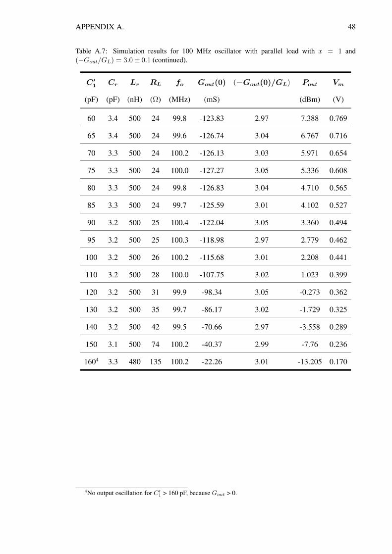
150 3.1 500 74 100.2 -40.37 2.99 -7.76 0.236
1604 3.3 480 135 100.2 -22.26 3.01 -13.205 0.170
4No output oscillation for C ′1 > 160 pF, because Gout > 0.

APPENDIX A. 49
Table A.8: Simulation results for 100 MHz oscillator with parallel load with x = 0.5 and(−Gout/GL) = 3.0± 0.1.
C′1 Cr Lr RL fo Gout(0) (−Gout(0)/GL) Pout Vm
(pF) (pF) (nH) (Ω) (MHz) (mS) (dBm) (V)
8 30 650 507 100.2 -5.92 3.00 13.52 7.163
9 45 560 278 100.5 -10.58 2.94 15.629 6.762
10 40 500 194 100.3 -15.5 3.01 16.663 6.363
11 13 500 147 100.3 -20.42 3.00 17.346 5.992
12 9 500 118 100.1 -25.18 2.98 17.799 5.663
13 7 500 98 100.3 -30.35 2.98 18.325 5.479
14 6 500 84 100.3 -35.77 3.00 18.821 5.368
15 5.4 500 73.6 100.4 -40.75 3.00 19.125 5.204
16 5.2 500 65 99.7 -45.85 2.98 18.564 4.584
17 4.8 500 59 100.1 -50.76 2.99 18.056 4.119
20 4.2 500 46 100.5 -64.72 2.98 17.386 3.367
30 3.7 500 29 99.9 -102.6 2.98 11.323 1.330
40 3.5 500 24 99.8 -127 3.05 7.953 0.821
50 3.3 500 21 100.5 -142 2.98 5.321 0.567
60 3.3 500 21 100.0 -146 3.07 3.273 0.448
70 3.2 500 22 100.4 -138 3.04 1.120 0.358
80 3.2 500 24 100.1 -126 3.02 -0.747 0.302
90 3.2 500 28 99.8 -106.49 2.98 -2.798 0.257
100 3.1 500 49 100.4 -61.34 3.01 -7.055 0.208
1055 3.1 500 62 100.3 -48.74 3.02 -9.430 0.178
5No output oscillation for C ′1 > 105 pF, because Gout > 0.

APPENDIX A. 50
Table A.9: Simulation results for 100 MHz oscillator with parallel load with x = 0.25 and(−Gout/GL) = 3.0± 0.1.
C′1 Cr Lr RL fo Gout(0) (−Gout(0)/GL) Pout Vm
(pF) (pF) (nH) (Ω) (MHz) (mS) (dBm) (V)
8 70 570 315 100.5 -9.53 3.00 15.372 6.988
9 15 540 201 100.5 -14.96 3.01 14.401 4.992
10 12 510 147 100.1 -20.23 2.97 16.117 5.201
11 8.9 500 114 99.7 -26.18 2.98 16.836 4.976
12 6.8 500 93 100.0 -32.31 3.00 16.729 4.439
13 5.8 500 78 100.1 -38.31 2.99 16.229 3.838
14 5.2 500 68 100.2 -44.43 3.02 15.543 3.311
15 4.9 500 59 99.9 -50.45 2.98 15.143 2.946
20 4.1 500 38 99.6 -78.93 3.00 13.567 1.972
25 3.7 500 29 100.1 -102.68 2.98 9.337 1.058
30 3.5 500 25 100.4 -121.11 3.03 6.187 0.684
35 3.4 500 22 100.4 -135.15 2.97 4.241 0.513
40 3.4 500 21 99.8 -145.71 3.06 2.552 0.412
45 3.3 500 20 100.2 -147.05 2.941 0.759 0.327
50 3.3 500 21 99.8 -144.3 3.03 -0.791 0.281
55 3.2 500 23 100.4 -130.99 3.01 -2.581 0.239
60 3.2 500 27 100.1 -110.68 2.99 -4.372 0.211
65 3.2 500 34 99.9 -89.08 3.03 -6.584 0.183
706 3.2 500 56 99.6 -53.63 3.00 -10.486 0.150
6No output oscillation for C ′1 > 70 pF, because Gout > 0.

51
APPENDIX B. SIMULATION RESULTS FOR 100MHZ CLAPP OSCILLATOR CONNECTED TO SERIESLOAD
Table B.1: Simulation results for 100 MHz oscillator with series load with x = 4 and(−Rout/RL) = 3.0± 0.1.
C′1 Cr Lr RL fo Rout(0) (−Rout(0)/RL) Pout Im
(pF) (pF) (nH) (Ω) (MHz) (Ω) (dBm) (mA)
15 20 500 3100 99.8 -9445 3.05 3.018 1.7
20 8 500 2918 99.8 -8987 3.08 4.302 2.0
30 5 500 2066 100.2 -6202 3.00 6.212 3.0
40 4.3 500 1534 100.0 -4543 2.96 7.534 4.1
50 4 500 1195 99.8 -3530 2.95 8.492 5.2
60 3.8 500 951 99.8 -2807 2.95 9.341 6.4
70 3.7 500 781 99.6 -2301 2.95 10.066 7.6
80 3.5 500 615 100.4 -1827 2.97 10.884 9.5
90 3.55 500 535 99.6 -1590 2.97 11.381 10.8
100 3.5 500 448 99.6 -1337 2.98 11.984 12.6
110 3.4 500 367 100.0 -1097 2.99 12.661 15.0
120 3.4 500 314 99.7 -943 3.00 13.183 17.3
130 3.4 500 270 99.5 -811 3.00 13.698 19.8
140 3.3 500 220 100.1 -662 3.01 14.390 23.7
150 3.3 500 190 99.9 -570 3.00 14.877 27.0

APPENDIX B. 52
Table B.2: Simulation results for 100 MHz oscillator with series load with x = 4 and(−Rout/RL) = 3.0± 0.1 (continued).
C′1 Cr Lr RL fo Rout(0) (−Rout(0)/RL) Pout Im
(pF) (pF) (nH) (Ω) (MHz) (Ω) (dBm) (mA)
160 3.3 500 164 99.7 -491 2.99 15.337 30.6
165 3.3 500 152 99.6 -456 3.00 15.558 32.6
168 3.3 500 145 99.6 -436 3.01 15.687 33.9
170 3.3 500 141 99.6 -423 3.00 15.77 34.7
171 3.2 500 130 100.4 -389 2.99 15.992 37.1
172 3.2 500 128 100.4 -383 2.99 16.028 37.5
173 3.2 500 126 100.4 -377 2.99 16.060 38.0
174 3.2 500 124 100.4 -371 2.99 16.087 38.4
175 3.2 500 122 100.4 -365 2.99 16.104 38.8
176 3.2 500 120 100.3 -359 2.99 16.101 39.1
177 3.2 500 118 100.3 -354 3.00 16.061 39.2
178 3.2 500 116 100.3 -349 3.01 15.993 39.3
179 3.2 500 115 100.3 -344 2.99 15.937 39.2
180 3.2 500 113 100.3 -338 2.99 15.860 39.2
181 3.2 500 111 100.3 -333 3.00 15.781 39.2
182 3.2 500 109 100.3 -328 3.01 15.701 39.2
183 3.2 500 108 100.3 -323 2.99 15.642 39.1
184 3.2 500 106 100.3 -317 2.99 15.559 39.1
185 3.2 500 104 100.2 -313 3.01 15.475 39.1
190 3.2 500 96 100.2 -289 3.01 15.089 38.9
200 3.2 500 82 100.1 -247 3.01 14.306 38.5

APPENDIX B. 53
Table B.3: Simulation results for 100 MHz oscillator with series load with x = 2 and(−Rout/RL) = 3.0± 0.1.
C′1 Cr Lr RL fo Rout(0) (−Rout(0)/RL) Pout Im
(pF) (pF) (nH) (Ω) (MHz) (Ω) (dBm) (mA)
30 4.2 500 436 100.0 -1178 2.706 8.916 9.0
35 4 500 422 99.9 -1230 2.91 9.206 9.4
40 3.8 500 448 100.1 -1343 3.00 9.579 9.5
45 3.7 500 483 99.9 -1460 3.02 10.175 9.8
50 3.6 500 476 100.0 -1437 3.02 10.806 10.7
55 3.5 500 430 100.3 -1291 3.00 11.395 12.0
60 3.5 500 404 99.9 -1234 3.05 11.842 13.0
70 3.4 500 336 100.1 -1008 3.00 12.826 16.0
80 3.4 500 290 99.6 -881 3.04 13.529 18.7
90 3.3 500 232 100.1 -695 3.00 14.370 23.0
100 3.3 500 197 99.8 -597 3.03 15.043 27.0
110 3.3 500 161 99.5 -499 3.10 15.736 32.4
120 3.2 500 128 100.1 -394 3.08 16.473 39.5
121 3.2 500 128 100.1 -385 3.01 16.499 39.6
122 3.2 500 126 100.1 -377 2.99 16.530 40.1
123 3.2 500 123 100.1 -368 2.99 16.544 40.6
124 3.2 500 120 100.1 -359 2.99 16.494 40.9
125 3.2 500 119 100.0 -358 3.01 16.414 40.7
130 3.2 500 106 100.0 -321 3.03 15.833 40.3
140 3.2 500 85 99.9 -260 3.06 14.631 39.2
6This value exceeds the maximum tolerance.

APPENDIX B. 54
Table B.4: Simulation results for 100 MHz oscillator with series load with x = 2 and(−Rout/RL) = 3.0± 0.1 (continued).
C′1 Cr Lr RL fo Rout(0) (−Rout(0)/RL) Pout Im
(pF) (pF) (nH) (Ω) (MHz) (Ω) (dBm) (mA)
150 3.2 500 68 99.8 -208 3.06 13.396 38.0
160 3.2 500 54 99.7 -166 3.07 12.121 36.9
170 3.1 500 37 100.5 -112 3.03 10.011 34.9
170 3.1 500 37 100.5 -112 3.03 10.011 34.9
180 3.1 500 28 100.4 -84 3.00 8.357 33.2
190 3.1 500 20 100.3 -59 2.95 6.276 30.9
200 3.1 500 12.67 100.2 -38 3.00 3.428 28.0

APPENDIX B. 55
Table B.5: Simulation results for 100 MHz oscillator with series load with x = 1 and(−Rout/RL) = 3.0± 0.1.
C′1 Cr Lr RL fo Rout(0) (−Rout(0)/RL) Pout Im
(pF) (pF) (nH) (Ω) (MHz) (Ω) (dBm) (mA)
35 3.7 500 37 100.1 -111 3.00 11.812 43.0
40 3.6 500 70 99.9 -205 2.93 13.039 36.0
45 3.5 500 97 100.0 -290 2.99 13.367 31.7
50 3.4 500 127 100.2 -382 3.01 14.016 29.9
60 3.4 500 121 99.6 -363 3.00 14.993 34.3
70 3.3 500 125 99.8 -384 3.07 15.979 37.8
75 3.3 500 121 99.6 -370 3.06 16.338 40.0
79 3.2 500 112 100.3 -336 3.00 16.708 43.4
80 3.2 500 107 100.3 -321 3.00 16.756 44.6
81 3.2 500 111 100.2 -333 3.00 16.747 43.8
82 3.2 500 107 100.2 -320 2.99 16.645 44.1
90 3.2 500 90 100.0 -274 3.04 16.441 46.9
100 3.2 500 68 99.8 -210 3.09 13.679 39.3
110 3.2 500 51 99.7 -157 3.08 11.843 36.7
120 3.1 500 35 100.4 -104 2.97 9.384 33.4
130 3.1 500 22.61 100.3 -67.82 3.00 6.664 30.4
140 3.1 500 12.66 100.2 -37.98 3.00 2.744 25.9
1507 3.1 500 4.38 100.1 -13.14 3.00 -4723 18.6
7No output oscillation for C ′1 > 150 pF, because Rout > 0.

APPENDIX B. 56
Table B.6: Simulation results for 100 MHz oscillator with series load with x = 0.5 and(−Rout/RL) = 3.0± 0.1.
C′1 Cr Lr RL fo Rout(0) (−Rout(0)/RL) Pout Im
(pF) (pF) (nH) (Ω) (MHz) (Ω) (dBm) (mA)
40 3.4 500 14 100.3 -41 2.93 12.915 79.3
42 3.4 500 17 100.1 -51 3.00 14.063 82.1
44 3.4 500 23.3 99.9 -70 3.00 15.104 79.1
45 3.4 500 25.2 99.8 -75.7 3.00 15.111 76.1
46 3.4 500 26.3 99.7 -79 3.00 14.933 73.0
47 3.4 500 27 99.6 -80.77 2.99 14.672 69.9
50 3.3 500 34 100.2 -101 2.97 14.036 57.9
55 3.3 500 35 99.9 -102.08 2.92 13.187 51.8
60 3.2 500 45.88 100.4 -137.63 3.00 13.298 45.8
65 3.2 500 43 100.2 -129 3.00 12.192 41.6
70 3.2 500 43 100.0 -128 2.98 11.57 38.8
75 3.2 500 36 99.9 -109 3.03 10.248 36.4
80 3.2 500 30 99.7 -89 2.97 8.895 34.1
85 3.2 500 24 99.6 -72 3.00 7.345 31.9
90 3.1 500 17 100.4 -50 2.94 4.774 28.2
95 3.1 500 11.48 100.3 -34.44 3.00 1.874 24.6
100 3.1 500 6.68 100.2 -20.03 3.00 -2.393 19.7
1058 3.1 500 2.11 100.1 -6.32 3.00 -11.768 11.9
8No output oscillation for C ′1 > 105 pF, because Rout > 0.

APPENDIX B. 57
Table B.7: Simulation results for 70 MHz oscillator with series load with x = 2 and(−Rout/RL) = 3.00± 0.01.
C′1 Cr Lr RL fo Rout(0) (−Rout(0)/RL) Pout
(pF) (pF) (nH) (Ω) (MHz) (Ω) (dBm)
30 45 500 95 71.0 -285 3.00 -1.861
40 22 500 145 70.3 -435 3.00 1.097
50 16 500 193 70.6 -580 3.01 3.510
60 13.5 500 256 70.8 -768 3.00 5.642
70 12.5 500 323 70.4 -968 3.00 7.317
80 11.5 500 367 70.7 -1101 3.00 8.597
90 11 500 403 70.6 -1209 3.00 9.019
100 10.6 500 417 70.6 -1250 3.00 9.412
110 10.2 500 420 70.8 -1259 3.00 9.939
120 10 500 418 70.7 -1255 3.00 10.440
130 10 500 393 70.3 -1179 3.00 10.859
140 10 500 389 69.9 -1167 3.00 11.244
150 10 500 403 69.5 -1209 3.00 11.586
160 10 500 386 69.2 -1159 3.00 11.947
170 10 500 343 69.0 -1028 3.00 12.345
180 9.8 500 334 69.2 -1003 3.00 12.770
190 9.6 500 304 69.5 -912 3.00 13.239
200 9.6 500 289 69.3 -867 3.00 13.562
220 9.4 500 265 69.4 -794 3.00 14.259
240 9.4 500 233 69.1 -699 3.00 14.853
260 9.2 500 194 69.4 -581 2.99 15.539
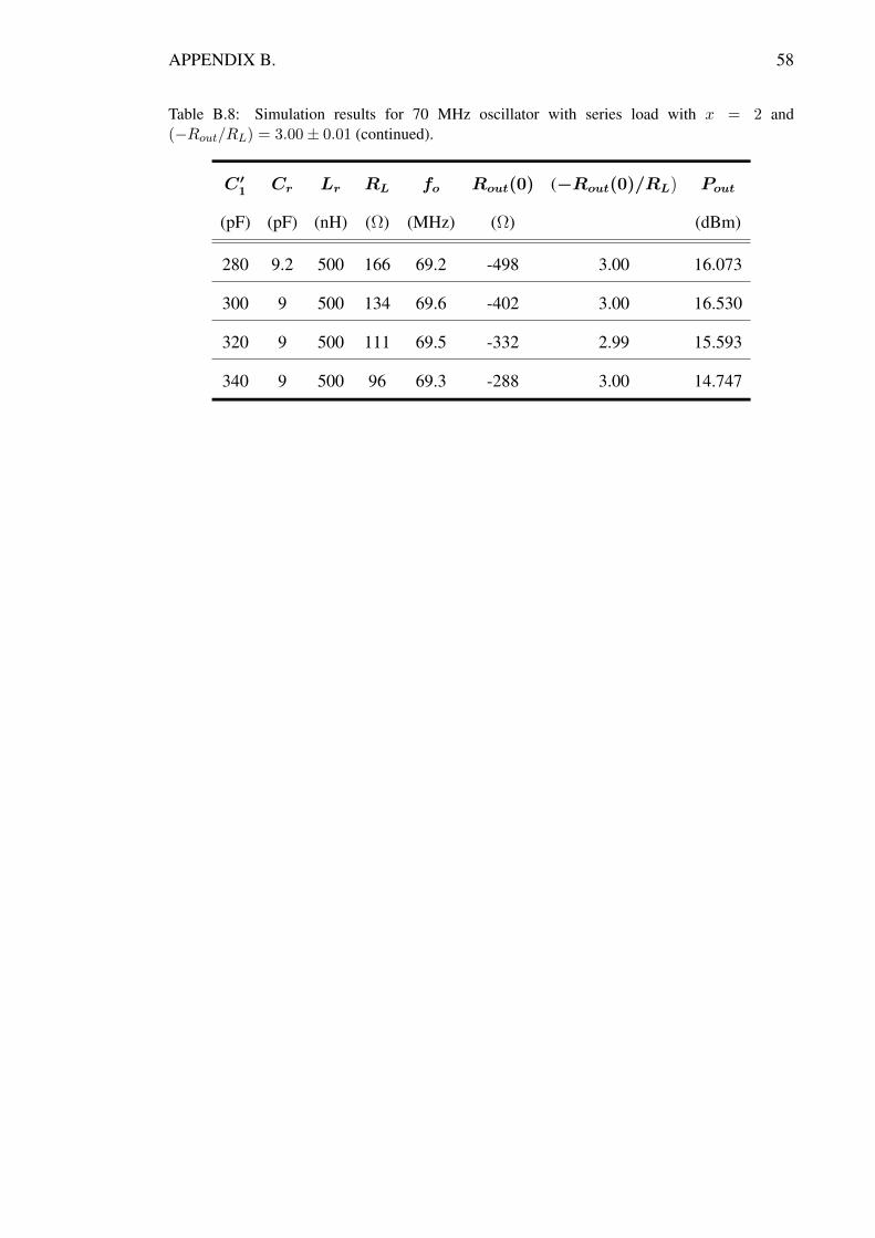
APPENDIX B. 58
Table B.8: Simulation results for 70 MHz oscillator with series load with x = 2 and(−Rout/RL) = 3.00± 0.01 (continued).
C′1 Cr Lr RL fo Rout(0) (−Rout(0)/RL) Pout
(pF) (pF) (nH) (Ω) (MHz) (Ω) (dBm)
280 9.2 500 166 69.2 -498 3.00 16.073
300 9 500 134 69.6 -402 3.00 16.530
320 9 500 111 69.5 -332 2.99 15.593
340 9 500 96 69.3 -288 3.00 14.747

59
APPENDIX C. G-V GRAPHS FOR THEOSCILLATOR WITH PARALLEL LOAD
Figure C.1: Simulation results for the small-signal output conductance Gout as a function of Vwith x = 1. a) Blue line: maximum power combination. b) Red line: maximum conductancecombination. c) Green lines: other combinations.

APPENDIX C. 60
Figure C.2: Simulation results for the small-signal output conductance Gout as a function of Vwith x = 0.5. a) Blue line: maximum power combination. b) Red line: maximum conductancecombination. c) Green lines: other combinations.
Figure C.3: Simulation results for the small-signal output conductance Gout as a function of Vwith x = 0.25. a) Blue line: maximum power combination. b) Red line: maximum conductancecombination. c) Green lines: other combinations.

61
APPENDIX D. R-I GRAPHS FOR THE OSCILLATORWITH SERIES LOAD
Figure D.1: Simulation results for the small-signal output resistance Rout as a function of I withx = 1. a) Blue line: maximum power combination. b) Red line: maximum resistance combina-tion. c) Green lines: other combinations.

APPENDIX D. 62
Figure D.2: Simulation results for the small-signal output resistance Rout as a function of I withx = 0.5. a) Blue line: maximum power combination. b) Red line: maximum resistance combina-tion. c) Green lines: other combinations.

63
APPENDIX E. RESONATOR INDUCTORCALCULATION
The goal here is to design a 500-nH air-wound coil with a high quality factor. The coil ismade from a copper wire with a diameter d = 0.8 mm. For a high quality factor, the spacebetween adjacent turns s was chosen such that space-to-diameter ratio (s/d) is equal to1.5. To calculate the number of turns needed, the following formula was used:
Lr =B2N2
0.45B + AFor A ≥ 0.4B, (E.1)
where B is the coil diameter in millimeters, A is the coil length in millimeters and N isthe number of turns.
The coil length A in terms of the number of turns was expressed as:
A = Ns
= N(1.5d)
= N(1.5)(0.8)
= 1.2N, (E.2)
and the coil diameter B was chosen to be 10 mm. By substituting coil parameters (A andB) in equation (E.1), the number of turns can be calculated as follows:
Lr =102N2
(0.45)(10) + 1.2N, (E.3)
100N2 − 600N − 2250 = 0, (E.4)
N =
8.6
or
−2.6 (rejected),
(E.5)
N = 8.6 ≈ 9 turns. (E.6)
To verify the condition mentioned in equation (E.1), we calculated A and found that
A = 1.2N = (1.2)(8.6) = 10.32 mm, (E.7)

APPENDIX E. 64
(note that A is approximatly equal to B, and that gives a higher quality factor)
0.4B = (0.4)(10) = 4 mm. (E.8)
From equations (E.7) and (E.8):A > 0.4B. (E.9)
Practically, a 500-nH inductor was designed using eight turns only. The final specifi-cations of the designed resonator inductor are shown in Table E.1.
Table E.1: Resonator inductor specifications.
Parameter Value
Wire diameter (d) 0.8 mm
Space between turns (s) 1.2 mm
Coil length (A) 9.6 mm
Coil diameter (B) 10 mm
Number of turns (N ) 8 turns
space to distance ratio (s/d) 1.5

65
APPENDIX F. TRANSISTOR BIASING
The aim here is to bias the transistor used to achieve an operating point VCEQ = 5 V andICQ = 20 mA using two resistor biasing circuit, and to know the value of the current thatshould be drawn from the DC source ICC .
For the oscillator connected to parallel load
The current gain (β) was unknown at the beginning, so a transient simulation was runseveral times for the circuit shown in Figure F.1. The DC source voltage (VCC) was fixedat 5 volts, while the two biasing resistors R1 and R2 were varied to achieve the desiredquiescent point (VCEQ = 5 V, ICQ = 20 mA). The final biasing settings are extractedfrom Figure F.1 and summarized in Table F.1.
Figure F.1: Clapp Oscillator schematic with DC annotations, where the load is connected in par-allel.
Table F.1: Transistor biasing settings for the oscillator with parallel load.
VCEQ ICQ VCC ICC R1 R2 VBE IB β
5 20 5 20.2 15.04 4.96 0.806 116 172.4
V mA V mA kΩ kΩ V µA

APPENDIX F. 66
If β were precisely known, then the following mathematical solution would have beencarried out. We assume the biasing equivalent circuit shown in Figure F.2, where all RFchokes and DC blocks are ideal. Applying KCL at node (1):
Figure F.2: Transistor equivalent biasing circuit.
ICC = I1 + IC . (F.1)
Applying KCL at node (2):I1 = I2 + IB. (F.2)
Substituting equation (F.2) in equation (F.1) :
ICC = I2 + IB + IC
= I2 +ICβ
+ IC
= I2 + (1 +1
β)IC . (F.3)
Considering β = 172.4:
ICC = I2 + (1 +1
172.4)(0.02) = (I2 + 0.0201) A. (F.4)

APPENDIX F. 67
Applying KVL at loop (1):
VCE = VBE + I1R1
= VBE + (I2 + IB)R1
= VBE + (I2 +ICβ
)R1 (F.5)
5 = 0.806 + (I2 +(20)(10−3)
172.4)R1, (F.6)
I2R1 + (1.16)(10−4)R1 − 4.194 = 0. (F.7)
Applying KVL at loop (2):
VBE = R2I2
= (20000−R1)I2 (F.8)
0.806 = (20000−R1)I2, (F.9)
20000I2 − I2R1 − 0.806 = 0. (F.10)
Solving equation (F.7) and (F.10) together by Matlab to find I2 and R1:
(I2, R1) =
160 µA, 15.047 kΩ
or
−28 µA, 48.056 kΩ (rejected because R1 > 20 kΩ).
(F.11)
Substituting I2 = 160 µA in equation (F.4) to find ICC :
ICC = I2 + 0.0201
= (160)(10−6) + 0.02012 = 20.28 mA, (F.12)
R2 = 20000−R1
= 20000− 15047 = 4.953 kΩ. (F.13)
The final results for ICC , R1 and R2 are similar to what are obtained by simulation.
For the oscillator connected to series load
The DC source voltage was set to 5.2 volts to compensate the RF choke voltage drop, asshown in Figure F.3. A transient simulations were done with varying R1 and R2 to obtainthe same desired quiescent point. The final biasing settings are shown in Table F.2.

APPENDIX F. 68
Figure F.3: Clapp Oscillator schematic with DC annotations, where the load is connected in series.
Table F.2: Transistor biasing settings for the oscillator with series load.
VCEQ ICQ VCC ICC R1 R2 VBE IB β
5 20 5.2 20.3 15.29 4.71 0.806 116 172.4
V mA V mA kΩ kΩ V µA
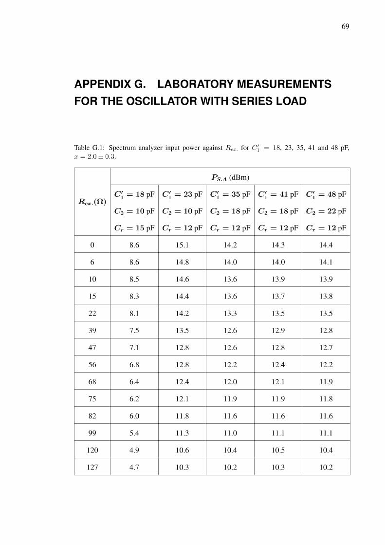
69
APPENDIX G. LABORATORY MEASUREMENTSFOR THE OSCILLATOR WITH SERIES LOAD
Table G.1: Spectrum analyzer input power against Rex. for C ′1 = 18, 23, 35, 41 and 48 pF,x = 2.0± 0.3.
Rex.(Ω)
PS.A (dBm)
C′1 = 18 pF C′
1 = 23 pF C′1 = 35 pF C′
1 = 41 pF C′1 = 48 pF
C2 = 10 pF C2 = 10 pF C2 = 18 pF C2 = 18 pF C2 = 22 pF
Cr = 15 pF Cr = 12 pF Cr = 12 pF Cr = 12 pF Cr = 12 pF
0 8.6 15.1 14.2 14.3 14.4
6 8.6 14.8 14.0 14.0 14.1
10 8.5 14.6 13.6 13.9 13.9
15 8.3 14.4 13.6 13.7 13.8
22 8.1 14.2 13.3 13.5 13.5
39 7.5 13.5 12.6 12.9 12.8
47 7.1 12.8 12.6 12.8 12.7
56 6.8 12.8 12.2 12.4 12.2
68 6.4 12.4 12.0 12.1 11.9
75 6.2 12.1 11.9 11.9 11.8
82 6.0 11.8 11.6 11.6 11.6
99 5.4 11.3 11.0 11.1 11.1
120 4.9 10.6 10.4 10.5 10.4
127 4.7 10.3 10.2 10.3 10.2

APPENDIX G. 70
Table G.2: Spectrum analyzer input power against Rex. for C ′1 = 18, 23, 35, 41 and 48 pF,x = 2.0± 0.3 (continued).
Rex.(Ω)
PS.A (dBm)
C′1 = 18 pF C′
1 = 23 pF C′1 = 35 pF C′
1 = 41 pF C′1 = 48 pF
C2 = 10 pF C2 = 10 pF C2 = 18 pF C2 = 18 pF C2 = 22 pF
Cr = 15 pF Cr = 12 pF Cr = 12 pF Cr = 12 pF Cr = 12 pF
151 4.2 9.5 9.6 9.7 9.7
182 3.3 8.3 8.7 8.9 8.7
268 1.7 6.2 6.9 7.1 7.0
329 0.7 4.9 5.7 5.8 5.8
400 -0.4 3.6 4.5 4.6 4.6

APPENDIX G. 71
Table G.3: Spectrum analyzer input power against Rex. for C ′1 = 55, 59, 64, 70 and 76 pF,x = 2.0± 0.3.
Rex.(Ω)
PS.A (dBm)
C′1 = 55 pF C′
1 = 59 pF C′1 = 64 pF C′
1 = 70 pF C′1 = 76 pF
C2 = 27 pF C2 = 27 pF C2 = 33 pF C2 = 33 pF C2 = 33 pF
Cr = 12 pF Cr = 12 pF Cr = 12 pF Cr = 12 pF Cr = 12 pF
0 14.7 14.5 15.3 15.4 15.5
6 14.5 14.3 15.2 15.3 15.4
10 14.4 14.1 15.0 15.1 15.2
15 14.3 14.0 14.9 14.9 15.0
22 14.0 13.7 14.3 14.7 14.8
39 13.4 13.1 14.1 14.0 14.2
47 13.2 13.0 13.9 13.7 14.0
56 12.8 12.5 13.5 13.4 13.6
68 12.6 12.3 13.2 13.0 13.3
75 12.4 12.2 13.1 12.8 13.1
82 12.2 11.6 12.9 12.5 12.9
99 11.6 11.4 12.3 12.0 12.3
120 11.0 10.8 11.6 11.3 11.6
127 10.8 10.7 11.5 11.0 11.5
151 9.9 10.1 10.7 10.4 10.9
182 8.6 9.2 9.9 9.3 10.0
268 7.5 7.4 7.9 None 7.9
329 6.3 6.2 6.6 None 6.6
400 5.0 4.9 5.2 None 5.2

APPENDIX G. 72
Table G.4: Spectrum analyzer power against Rex. for C ′1 = 88, 103, 109, and 128 pF,x = 2.0± 0.3.
Rex.(Ω)
PS.A (dBm)
C′1 = 88 pF C′
1 = 103 pF C′1 = 109 pF C′
1 = 128 pF
C2 = 47 pF C2 = 56 pF C2 = 56 pF C2 = 68 pF
Cr = 10 pF Cr = 10 pF Cr = 10 pF Cr = 10 pF
0 15.6 14.6 14.6 14.4
6 15.3 14.4 14.5 14.3
10 15.1 14.4 14.4 14.1
15 14.9 14.2 14.3 14.0
22 14.7 14.0 14.0 13.8
39 14.0 13.5 13.5 13.3
47 13.8 13.1 13.3 12.9
56 13.2 12.8 13.0 12.6
68 13.2 12.6 12.7 12.3
75 12.9 12.3 12.3 12.0
82 12.7 12.1 12.1 11.7
99 12.1 11.4 11.5 10.8
120 11.5 10.8 10.9 10.1
127 11.3 10.4 10.6 9.2
151 10.6 9.6 None 8.6
182 9.6 8.4 8.5 None
268 7.4 None None None
329 6.0 None None None
400 None None None None