b be b ce vidyalankarengineering.vidyalankar.org/prelim-papers/se/cmpn/eccf_soln.pdfvidyalankar :...
TRANSCRIPT
1
S.E. Sem. III [CMPN] Electronic Circuits and Communication Fundamentals
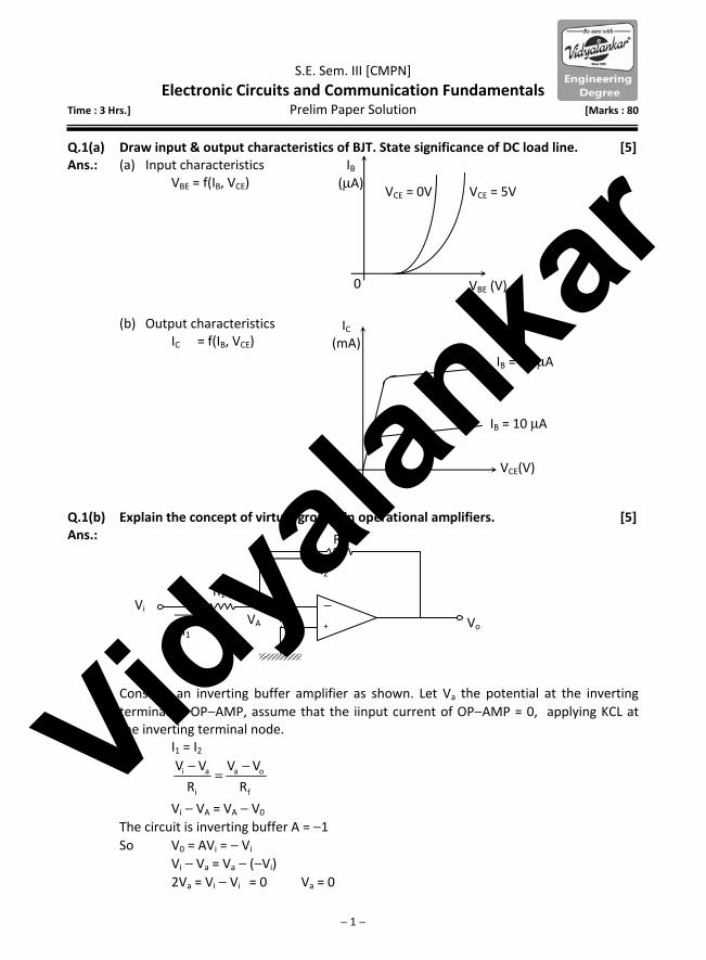
Time : 3 Hrs.] Prelim Paper Solution [Marks : 80 Q.1(a) Draw input & output characteristics of BJT. State significance of DC load line. [5] Ans.: (a) Input characteristics VBE = f(IB, VCE) (b) Output characteristics IC = f(IB, VCE) Q.1(b) Explain the concept of virtual ground in operational amplifiers. [5] Ans.: Consider an inverting buffer amplifier as shown. Let Va the potential at the inverting
terminal of OPAMP, assume that the iinput current of OPAMP = 0, applying KCL at the inverting terminal node.
I1 = I2
i a a o
i f
V V V VR R
Vi VA = VA V0 The circuit is inverting buffer A = 1 So V0 = AVi = Vi Vi Va = Va (Vi) 2Va = Vi Vi = 0 Va = 0
IB
(A)
VBE (V)
VCE = 0V VCE = 5V
0
IC
(mA)
VCE(V) 0
IB = 20 A
IB = 10 A
+
Rf
R1
Vo
Vi VA VB
I1
I2
Vidyalan
kar
Vidyalankar : S.E. – Maths III
2
Very few OPAMPS for eg. 301, 748 & 777 have the OFFSET. Voltage null capability. Hence for most of the OPAMPS we have to design an OFFSET voltage corpersation network in order to reduce the ouptu offset voltage to zero.
Q.1(c) Compare class A and class C amplifier. [5] Ans.: In this class-A, amplifier operates in active region at all the times(2*π). • Stage efficiency = PoAC)/ PDC 100 % Conduction angle 2 Conversion efficiency = 50% • Load Power, PL = (VL)
2/RL = (VPP)2/8*RL • In this class-C, amplifier operates for less than half of the input cycle(less than π). • It is basically a tuned amplifier. • AC load power for class-C amplifier is, PL = (VPP)2/8*RL Where, VPP is peak to peak load voltage and RL is load resistance Conduction angle less than Conversion efficiency ≈ 90% Q.1(d) Explain adaptive delta modulation. [5] Ans.: Delta modulation is also a digital modulation system. In delta modulation just one bit is sent
per sample, to indicate whether the present sample is larger or smaller than the previous sample. Thus in delta modulation, the modulated signal carries information not about the signal samples but about the difference between successive samples. If the difference is +ve or ve a +ve or ve pulse respectively is generated in the modulated signal. Thus D.M. carries the information about the derivative of m(t) and hence the name is delta modulation. Thus integration of delta modulated signal m (t) will be an approximation of m (t).
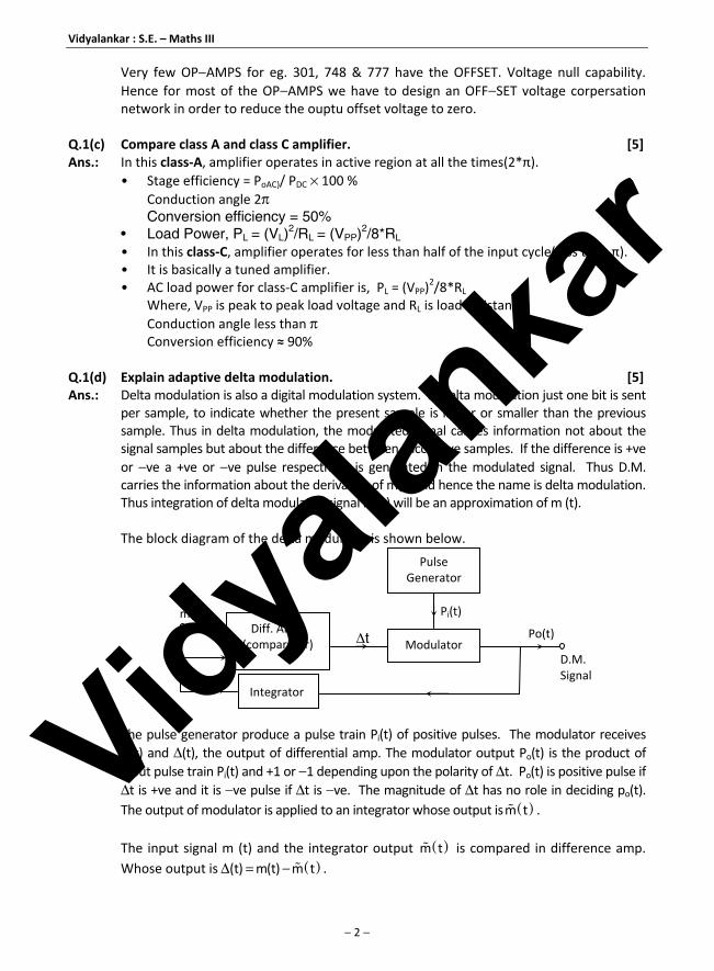
The block diagram of the delta modulator is shown below. The pulse generator produce a pulse train Pi(t) of positive pulses. The modulator receives
Pi(t) and (t), the output of differential amp. The modulator output Po(t) is the product of input pulse train Pi(t) and +1 or 1 depending upon the polarity of t. Po(t) is positive pulse if t is +ve and it is ve pulse if t is ve. The magnitude of t has no role in deciding po(t). The output of modulator is applied to an integrator whose output is m t .
The input signal m (t) and the integrator output m t is compared in difference amp.
Whose output is (t) m(t) m t .
Integrator
Pulse Generator
Modulator Diff. Amp.
(comparator) D.M. Signal
Po(t) t
m t
Pi(t)m(t)
Vidyalan
kar
Prelim Paper Solution
3
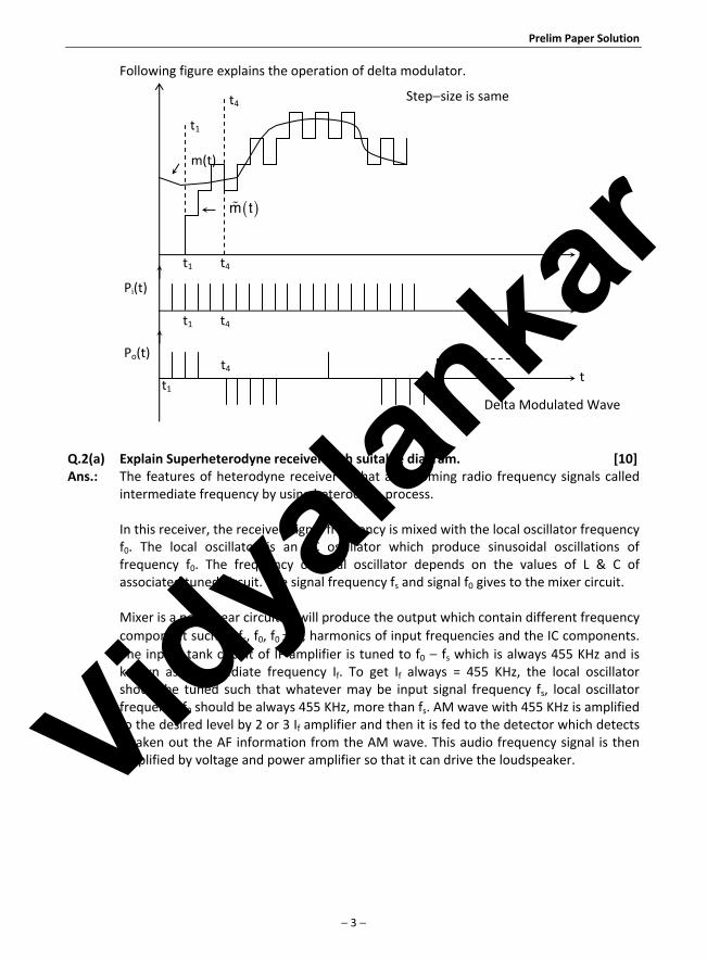
Following figure explains the operation of delta modulator. Q.2(a) Explain Superheterodyne receiver with suitable diagram. [10] Ans.: The features of heterodyne receiver is that all incoming radio frequency signals called
intermediate frequency by using heterodyne process. In this receiver, the received signal frequency is mixed with the local oscillator frequency
f0. The local oscillator is an LC oscillator which produce sinusoidal oscillations of frequency f0. The frequency of local oscillator depends on the values of L & C of associated tuned circuit. The signal frequency fs and signal f0 gives to the mixer circuit.
Mixer is a non-linear circuit. It will produce the output which contain different frequency
component such as fs, f0, f0 fs, harmonics of input frequencies and the IC components. The inputs tank circuit of IF amplifier is tuned to f0 fs which is always 455 KHz and is known as Intermediate frequency If. To get If always = 455 KHz, the local oscillator should be tuned such that whatever may be input signal frequency fs, local oscillator frequency f0 should be always 455 KHz, more than fs. AM wave with 455 KHz is amplified to the desired level by 2 or 3 If amplifier and then it is fed to the detector which detects a taken out the AF information from the AM wave. This audio frequency signal is then amplified by voltage and power amplifier so that it can drive the loudspeaker.
Delta Modulated Wave
t
Po(t)
t1 t4
Pi(t)
t
t1
t4
m t
m(t)
Stepsize is same
t1 t4
t1 t4
Vidyalan
kar
Vidyalankar : S.E. – Maths III
4
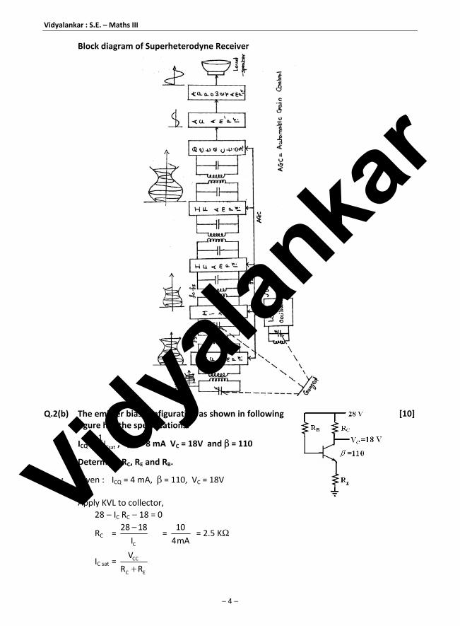
Block diagram of Superheterodyne Receiver Q.2(b) The emitter bias configuration as shown in following
figure has the specifications:
ICQ = Csat1
I2
, ICsat = 8 mA VC = 18V and = 110
Determine RC, RE and RB.
[10]
Ans.: Given : ICQ = 4 mA, = 110, VC = 18V Apply KVL to collector, 28 IC RC 18 = 0
RC =
C
28 18I
= 104mA
= 2.5 K
IC sat = CC
C E
VR R
Vidyalan
kar

Prelim Paper Solution
5
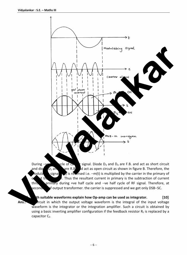
During +ve half cycle of carrier.Fig. (a)
During ve half cycle of carrier. Fig. (b)
8 mA = E
282.5K R
RE = 1 k
IB = CI = 36.3 A
IB =
CC BE
B E
V VR (1 )R
= B
28 0.7R (1 110)
RB = 639.82 k Q.3(a) Explain generation of DSBSC using Ring Modulator. [10] Ans.: The ring modulator is also known as Lattice or double balanced modulator. In this
circuit, four diodes are connected in same direction and they will form a ring. Hence the name Ring Modulator.
During +ve half cycle of carrier signal diode D1 and D2 are forward biased and acts as
short circuit and diode D3 and D4 are reverse biased and act as open circuit as shown in figure A. Therefore, the modulating signal multiplies with the carrier signal, in the primary of output transformer.
Vidyalan
kar
Vidyalankar : S.E. – Maths III
6
During ve half cycle of carrier signal. Diode D3 and D4 are F.B. and act as short circuit
and diode D1 and D2 are R.B. and act as open circuit as shown in figure B. Therefore, the modulating signal m(t) is reversed i.e. m(t) is multiplied by the carrier in the primary of output transformer. Thus the resultant current in primary is the subtraction of current through primary during +ve half cycle and ve half cycle of RF signal. Therefore, at secondary of output transformer. the carrier is suppressed and we get only DSBSC.
Q.3(b) With suitable waveforms explain how Op-amp can be used as integrator. [10] Ans.: A circuit in which the output voltage waveform is the integral of the input voltage
waveform is the integrator or the integration amplifier. Such a circuit is obtained by using a basic inverting amplifier configuration if the feedback resistor RF is replaced by a capacitor CF.
Vidyalan
kar

Prelim Paper Solution
7
Expression for output of basic integrator Fig.(a) The expression for output V0 can be obtained by writing KCL equation at node V2. Iin = IB2 + Ic Since IB2 = 0 Iin = Ic
Cin 2F
1
dVV VC
R dt ( VC = V2 V0)
2 0in 2F
1
d(V V )V VC
R dt
However, V1 = V2 = 0, because A is very large.
0inF
1
dV ( )VC
R dt.
Integrate both sides with respect to time t.
inF 0
1
V ddt C ( V )
R dt
0 in1 F
1V V dt
R C (A)
The equation (A) shows that output voltage is directly proportional to time constant RFCF.
t (sec)
Vin
0
1V
1V
t (sec)
0.5 1.5
0
Fig. (a) : Basic Integrator
VC CF
RL
Vin ~
R1
V0 = in1 F
1V dt
R C
Iin
V2 Ic IB2
IB1
Vcc
-VCC
Vidyalan
kar

Vidyalankar : S.E. – Maths III
8
Q.4(a) For an AM DSBFC envelope with Vmax = 20V and Vmin = 4V; determine : (i) Peak amplitude of USF and LSF (ii) Peak amplitude of carrier (iii) Peak change in the amplitude of envelope (iv) Modulation coefficient (v) Draw the AM Envelope
[10]
Ans.: Given : Vmax = 20V and Vmin = 4V
(ii) Peak amplitude of carrier
VC = max minV V2
= 20 42
= 242
= 12 V
Vm = max minV V2
= 20 42
= 162
= 8 V
(iii) Peak change in the amplitude of envelope 4V
(iv) Modulation coefficient
m = m
C
VV
= 812
= 0.666
(i) Peak amplitude of USF and LSF
AUSB = ALSB = CmV2
= 3.96 V
(v) Draw the AM Envelope Q.4(b) Draw the PAM, PPM and PWM waveforms and compare them. [5] Ans.:
Parameter PAM PWM PPM (i) Information contained in Amplitude
Variation Width
Variation Position Variation
(ii) Bandwidth Requirement low high high (iii) Noise immunity low high high (iv) Transmitted Power Varies with
amplitude & pulses
Varies with variation in
width
Remains constant
(v) Need to transmit synchronization pulses not needed not needed necessary (vi) Complexity of generation & detection Complex Easy Complex
VAM Vmax
Vmin
t
Vidyalan
kar

Prelim Paper Solution
9
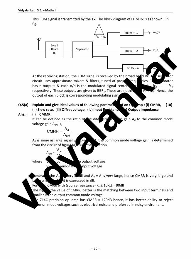
Q.4(c) Explain principle of FDM. [5] Ans.: FDM consists of simultaneous transmission of message of different channels by shifting them
in frequency domain. The bock diagram of FDM Tx & Rx is as shown below. In above diagram, all the base band carrier blocks are the amplitude modulators. Here,
all the signals have the same frequency spectrum. Therefore, all these signals are upshifted in different frequency slot using amplitude modulator. For every BBC Block, the carrier frequency is different. Hence the output of BBC 1 will be fC1 fm1. The output of BBC 2 will be fC2 fm2. If all the modulating signals have the same B.W. then output of Adder will have the following spectrum.
Sig 1
Sig 2
Sig 3
Sig n
Baseband Carrier 1
BBC 2
BBC 3
BBC n
A d d e r
AM
TX
m n(t)
m3(t)
m2(t)
m1(t)
2fm fm2 fc2 fcn fmn fc1
2fm
fm1 Vidyalan
kar
Vidyalankar : S.E. – Maths III
10
This FDM signal is transmitted by the Tx. The block diagram of FDM Rx is as shown in fig.
At the receiving station, the FDM signal is received by the broad band Rx. The separator
circuit uses approximate mixers & filters, tuned at proper frequencies. The separator has n outputs & each o/p is the modulated signal centered around fc1, fc2 fcn respectively. These outputs are given to BBRX. These are nothing but AM Rxs. Hence the output of each block is corresponding modulating signal.
Q.5(a) Explain and give ideal values of following parameters of an Op-Amp : (i) CMRR,
(ii) Slew rate, (iii) Offset voltage, (iv) Input Resistance, (v) Output Impedance [10]
Ans.: (i) CMMR : It can be defined as the ratio of the diferential voltage gain Ad to the common mode
voltage gain Acm is,
d
cm
ACMRR
A
Ad is same as large signal voltage gain A. the common mode voltage gain is determined from the circuit of figure (a) using the equation,
Acm = ocm
cm
VV
where Vocm = common mode output voltage Vcm = common mode input voltage Generally, the Acm is very small and Ad = A is very large, hence CMRR is very large and
being a large value it is expressed in dB. For 741C CMRR with (source resistance) Rs 10k = 90dB The higher the value of CMRR, better is the matching between two input terminals and
smaller is the output common mode voltage. The 714C precision opamp has CMRR = 120dB hence, it has better ability to reject
common mode voltages such as electrical noise and preferred in noisy enviroment.
BroadBand
Rx
Separator
BB Rx 1
BB Rx 2
BB Rx n mn(t)
m1(t)
m2(t)
fc1 fm1
Vidyalan
kar
Prelim Paper Solution
11
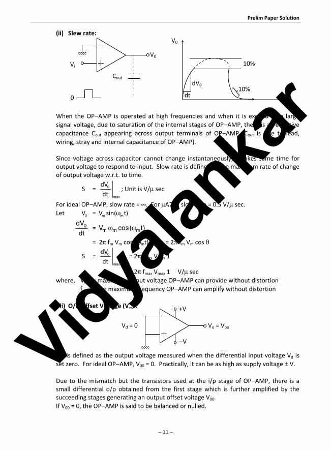
(ii) Slew rate: When the OPAMP is operated at high frequencies and when it is excited by a large
signal voltage, due to saturation of the internal stages of OPAMP, there is an effective capacitance Cout appearing across output terminals of OPAMP (Cout is due to lead, wiring, stray and internal capacitance of OPAMP).
Since voltage across capacitor cannot change instantaneously, it takes same time for
output voltage to respond to input. Slow rate is defined as the maximum rate of change of output voltage w.r.t. to time.
S = 0
max
dVdt
; Unit is V/ sec
For ideal OPAMP, slow rate = . For A741 slow rate = 0.5 V/ sec. Let 0V = m mV sin( t)
0dVdt
= m m mV cos( t)
= 2 fm Vm cos (mt) = 2 fm Vm cos
S = 0
max
dVdt
= 2 fmax Vmax 1
= 2 fmax Vmax 1 V/ sec where, Vmax = maximum output voltage OPAMP can provide without distortion fmax = The maximum frequency OPAMP can amplify without distortion (iii) O/P Offset Voltage (V) : V00 is defined as the output voltage measured when the differential input voltage Vd is
set zero. For ideal OPAMP, V00 = 0. Practically, it can be as high as supply voltage V. Due to the mismatch but the transistors used at the i/p stage of OPAMP, there is a
small differential o/p obtained from the first stage which is further amplified by the succeeding stages generating an output offset voltage V00.
If V00 = 0, the OPAMP is said to be balanced or nulled.
V
+V
Vo = Voo Vd = 0
dt
dV0
V0
t
10%
10%
V0 Vi
Cout
0
Vidyalan
kar
Vidyalankar : S.E. – Maths III
12
(iv) Input resistance (Ri) : It is defined as resistance which can be measured at either the inverting or non-inverting
terminal with the other terminal connected to ground. It is few mega for transistor input stage and extremely high (thousand of G) for op-
amp having FET based input stages. Ri = 2M. (v) Output Resistance (Ro) : Output resistance Ro is the equivalent resistance that can be measured between the
output terminal of the opamp and the ground. It is 75 for 741C opamp. Q.5(b) Define and explain in brief Amount of information, average information,
information rate and Channel capacity of a communication system. [10]
Ans.: The more the probability of an event the less is the amount of information associated with it and vice versa.
Thus we can define “Information as reciprocal of probability”
i.e.
K 2K
1I log
P … (1)
IK is the information of event ‘k’ with probability PK
The unit of information is ‘bit’ when the base of log is ‘2’ for base ‘e’ the unit is ‘hat’ for base 10. Unit is decit or Harley.
"Actually information is dimensionless quantity” Average Information : The “Entropy” is defined as average information per message. It
is denoted by ‘H’ and its unit is bits/message. It is given by
H =
M
k 2 KK 1
P log P … (1)
This expression indicates that the entropy of a source is depends only on the probabilities.
Information Rate : If a message source generates message is at rate of ‘r’ messages per second. Then the
rate of information " ‘R’ is defined as average number of bits of information per second". [Average information per second]
We know ‘H’ is the average number of bits of information per message Hence R = r.H bits/sec. If the source of message generates 'r' number of messages per second then. Information
rate is given by R = r H r No. of messages / sec H Message information / message
R =
Message Average Informationr H
Sec message
R = Av. Information / Sec bits / sec.
Vidyalan
kar

Prelim Paper Solution
13
Channel Capacity The channel capacity is defined as the maximum possible bit rate a channel can support
without introducing any error. i.e. channel capacity is the maximum of mutual information.
C = max I (x ; y) bits/sec The channel capacity is a function of only transition probabilities P(yj/xi) which define
the channel. Channel capacity is defined as maximum average mutual information in any single use
of the channel (i.e. signaling interval) The transmission efficiency or channel efficiency is defined as
Actual transinformation
Maximum transinformation
Q.6(a) Implement using IC 741, Vo = 3V1 4V2 + 5V3 6V4 V5 [5] Ans.: Vo = 3V1 4V2 + 5V3 6V4 V5 = (3V1 + 5V3) (4V2 + 6V4 + V5) Q.6(b) Write a note on Pulse Code Modulation with waveforms. [5] Ans.: Following fig. shows the block diagram of the P.C.M. system. Sampler : The incoming modulating signal is sampled with a train of narrow rectangular
pulses. The sampling rate must be greater than twice the highest modulating frequency > 2 fm(max).
Low PassFilter
Sampler
Quantizer Encoder m(t)
PCM Wave
4.72.9 2.1 5
3 2
Analog to digital converter
1 10 0 1 1 0 0 1
5 3 2
0
0 1 0 1
V1
V3
+VCC
VEE
10 K
Rf R1
3.33 K
R3
2 K
V01
V2
V4
V5
R
10 K
R2
2.5 K
R4
1.66 K
R5
10 K
+VCC
VEE
10 K
Rf
V0
V01 = [3V1 + 5v3]
Vidyalan
kar
Vidyalankar : S.E. – Maths III
14
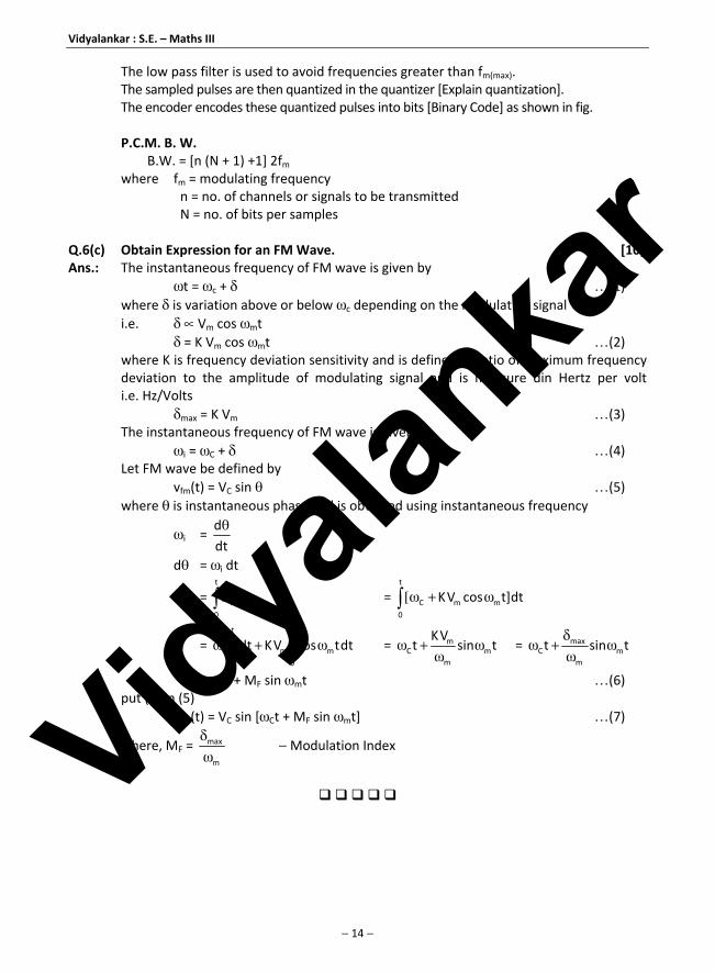
The low pass filter is used to avoid frequencies greater than fm(max). The sampled pulses are then quantized in the quantizer [Explain quantization]. The encoder encodes these quantized pulses into bits [Binary Code] as shown in fig. P.C.M. B. W. B.W. = [n (N + 1) +1] 2fm where fm = modulating frequency n = no. of channels or signals to be transmitted N = no. of bits per samples Q.6(c) Obtain Expression for an FM Wave. [10] Ans.: The instantaneous frequency of FM wave is given by t = c + (1) where is variation above or below c depending on the modulating signal i.e. Vm cos mt = K Vm cos mt (2) where K is frequency deviation sensitivity and is defined as ratio of maximum frequency
deviation to the amplitude of modulating signal and is measure din Hertz per volt i.e. Hz/Volts
max = K Vm (3) The instantaneous frequency of FM wave is given by i = C + (4) Let FM wave be defined by vfm(t) = VC sin (5) where is instantaneous phase and is obtained using instantaneous frequency
i = ddt
d = i dt
= t
i0
dt = t
C m m0
KV cos t]dt
= t t
C m m0 0
dt KV cos tdt =
mC m
m
KVt sin t =
max
C mm
t sin t
= Ct + MF sin mt (6) put (6) in (5) vfm(t) = VC sin [Ct + MF sin mt] (7)
where, MF = max
m
Modulation Index
Vidyalan
kar