bachelor thesis presentation slides
DESCRIPTION
ÂTRANSCRIPT

Outline
PMMA-thin films as dielectric layer for printable field effect transistors
Levon Altunyan
Fakultat fur IngenieurwissenschaftenNanostrukturtechnik
Universitat Duisburg-Essen
April 28, 2009
Levon Altunyan Universitat Duisburg-Essen - Fakultat fur Ingenieurwissenschaften, Nanostrukturtechnik
PMMA-thin films as dielectric layer for printable field effect transistors

Aim of the WorkMIM Development
MeasurementsTransistorSummary
Outline
1 Aim of the Work
2 MIM DevelopmentSpin Coating ProcessI-V measurements
3 MeasurementsC-V measurements; Static dielectric constant, Part IMeasurements of the static dielectric constant, Part IIBreakdown voltageBreakdown field strenght
4 TransistorMISFET devices
5 SummaryResultsFuture Work
Levon Altunyan Universitat Duisburg-Essen - Fakultat fur Ingenieurwissenschaften, Nanostrukturtechnik
PMMA-thin films as dielectric layer for printable field effect transistors

Aim of the WorkMIM Development
MeasurementsTransistorSummary
Objectives
The main aims of this work are:
PMMA as gate dielectric
Development of a metal insulator metal (MIM) structure
I-V and C-V measurements of the MIM structures
Measurement of the static dielectric constant (εPMMA)
Measurement of the breakdown voltage and breakdown field strenght of PMMA
Realization of MISFET devices (PMMA as gate dielectric)
Levon Altunyan Universitat Duisburg-Essen - Fakultat fur Ingenieurwissenschaften, Nanostrukturtechnik
PMMA-thin films as dielectric layer for printable field effect transistors

Aim of the WorkMIM Development
MeasurementsTransistorSummary
Spin Coating ProcessI-V measurements
Set of the initial spin coating procedure parameters
1000 2000 3000 4000 5000 6000 7000
400
450
500
550
600
650
Spin Speed, ω [rpm] →
Film
thic
kness, h [nm
] →
PMMA Layer Thickness (nm) vs. Spin Speed (rpm)
h = k1ωα
Use of 2 phases:First Spin parameters:
ω = 1000(rpm)
a = 500(rpm/s2)t = 20(s)
Second Spin parameters:ω ∈ [1000(rpm); 7000(rpm)]stepsize = 500(rpm)
a = 500(rpm/s2)t = 60(s)
Baking Conditions:Tannealing = 120(◦C)tannealing = 50(min)
Preparation of 1 sample/step sizePMMA layer thickness measured at 8points/sample
Levon Altunyan Universitat Duisburg-Essen - Fakultat fur Ingenieurwissenschaften, Nanostrukturtechnik
PMMA-thin films as dielectric layer for printable field effect transistors

Aim of the WorkMIM Development
MeasurementsTransistorSummary
Spin Coating ProcessI-V measurements
Optimized Spin Coating process forthe low viscosity PMMAsupplied by Evonik:
1 spin only
tspin = 25(s)
Max acc., a = 10000(rpm/s2)
tannealing = 30(min)
Tannealing = 160(◦C)
1000 2000 3000 4000 5000 6000
300
400
500
600
700
800
900
Spin Speed, ω [rpm] →
Film
thic
kness, h [nm
] →
PMMA Layer Thickness (nm) vs. Spin Speed (rpm)
h = k1ωα
Conclusions:
The fit curve d(ω) = k1 ∗ (ω(−α)) [1] should be seen only as a good reference for thegeneral behavior of the measured set of data points.
Less scatering in the layer hights (ω > 1700(rpm)).
Results correspond better to the thicknesses given by the material data provided byEvonik for wt% = 4, 5(%).
Levon Altunyan Universitat Duisburg-Essen - Fakultat fur Ingenieurwissenschaften, Nanostrukturtechnik
PMMA-thin films as dielectric layer for printable field effect transistors

Aim of the WorkMIM Development
MeasurementsTransistorSummary
Spin Coating ProcessI-V measurements
I-V measurements
−1 −0.5 0 0.5 1−1.5
−1
−0.5
0
0.5
1
1.5x 10⁶
Voltage, V [V] →
Cur
rent
, I [n
A] →
Critical issue when using the initial MIM structure - High leackage currents havebeen observed.
Different scenarios for the possible reasons have been taken into consideration:Diffusion of the Silver contacts inside the PMMA layer;Probability that during measurements, the top contact’s electrode probe penetratesthrough, and touches the bottom contact;
Levon Altunyan Universitat Duisburg-Essen - Fakultat fur Ingenieurwissenschaften, Nanostrukturtechnik
PMMA-thin films as dielectric layer for printable field effect transistors

Aim of the WorkMIM Development
MeasurementsTransistorSummary
Spin Coating ProcessI-V measurements
New Contacts Arrangement
To decrease the probability that during measurements, the top contact’s probepenetrates through, and touches the bottom contact and causes high leackagecurrents, a special design has been taken into cosideration.
High leakage current problems persisted.Conclusion - Silver is dissolving inside the PMMA layer, which is the reason for thehigh leakage currents observed.
Levon Altunyan Universitat Duisburg-Essen - Fakultat fur Ingenieurwissenschaften, Nanostrukturtechnik
PMMA-thin films as dielectric layer for printable field effect transistors

Aim of the WorkMIM Development
MeasurementsTransistorSummary
Spin Coating ProcessI-V measurements
−10 −8 −6 −4 −2 0 2 4 6 8 10−500
0
500Current/Voltage Characteristic
Voltage [V] →
Cur
rent
[nA
] →
−10 −8 −6 −4 −2 0 2 4 6 8 10−0.01
−0.005
0
0.005
0.01Current/Voltage Characteristic
Voltage [V] →
Cur
rent
[nA
] →
Material for the bottom and top contacts changed to Aluminium.
”Crossed” contacts design + Aluminium = low leakage currents.
The structure of the sucesfully eliminating contacts interconnections MIM structure canbe summarized as follows:
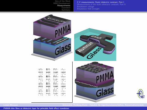
Use of aluminium metalized contacts:25(nm) ≤ Albottom ≤ 50(nm)50(nm) ≤ Altop ≤ 75(nm)
Use of the ”crossed contacts” design type
Levon Altunyan Universitat Duisburg-Essen - Fakultat fur Ingenieurwissenschaften, Nanostrukturtechnik
PMMA-thin films as dielectric layer for printable field effect transistors

Aim of the WorkMIM Development
MeasurementsTransistorSummary
C-V measurements; Static dielectric constant, Part IMeasurements of the static dielectric constant, Part IIBreakdown voltageBreakdown field strenght
400 450 500 550 60040
50
60
70
80
90
100
PMMA Layer Thickness, dPMMA
[nm] →
Cap
acita
nce,
C [p
F] →
400 450 500 550 6000
50
100
150
200
PMMA Layer Thickness, dPMMA
[nm] →
Cap
acita
nce,
C [p
F] →
400 450 500 550 6000
5
10
15
20
25
30
PMMA Layer Thickness, dPMMA
[nm] →
Die
lect
ric C
onst
ant,
εPM
MA
[−] →
400 450 500 550 60010
20
30
40
50
PMMA Layer Thickness, dPMMA
[nm] →
Die
lect
ric C
onst
ant,
εPM
MA
[−] →
Levon Altunyan Universitat Duisburg-Essen - Fakultat fur Ingenieurwissenschaften, Nanostrukturtechnik
PMMA-thin films as dielectric layer for printable field effect transistors
Aim of the WorkMIM Development
MeasurementsTransistorSummary
C-V measurements; Static dielectric constant, Part IMeasurements of the static dielectric constant, Part IIBreakdown voltageBreakdown field strenght
Levon Altunyan Universitat Duisburg-Essen - Fakultat fur Ingenieurwissenschaften, Nanostrukturtechnik
PMMA-thin films as dielectric layer for printable field effect transistors

Aim of the WorkMIM Development
MeasurementsTransistorSummary
C-V measurements; Static dielectric constant, Part IMeasurements of the static dielectric constant, Part IIBreakdown voltageBreakdown field strenght
0 0.02 0.04 0.06 0.08 0.1 0.12 0.14
1
2
3
4
5
Area, A [mm2] →
Die
lect
ric C
onst
ant,
ε PM
MA [−
] →
0 0.02 0.04 0.06 0.08 0.1 0.12 0.142
3
4
5
6
Area, A [mm2] →
Die
lect
ric C
onst
ant,
ε PM
MA [−
] →
0 0.02 0.04 0.06 0.08 0.1 0.12 0.142.5
3
3.5
4
4.5
5
5.5
6
Area, A [mm2] →
Die
lect
ric C
onst
ant,
ε PM
MA [−
] →
350 400 450 500 550 600 650 7000
1
2
3
4
5
PMMA Layer Thickness, dPMMA
[nm] →
Die
lect
ric C
onst
ant,
ε PM
MA [−
] →
Figure: Dielectric Constant (ε) vs. Contacts Area, dPMMA ≈ a.)375; b.)475; c.)700 (nm)
Levon Altunyan Universitat Duisburg-Essen - Fakultat fur Ingenieurwissenschaften, Nanostrukturtechnik
PMMA-thin films as dielectric layer for printable field effect transistors

Aim of the WorkMIM Development
MeasurementsTransistorSummary
C-V measurements; Static dielectric constant, Part IMeasurements of the static dielectric constant, Part IIBreakdown voltageBreakdown field strenght
Dielectric Constant, Results and Discussion
Results:
Higher capacitance values for lower PMMA layer hight observed.
Low frequency dependency (< 1%) of the (C-V) characteristics (f=100 kHz, f=1MHz).
A few values deviate highly from the majority of points.Consequence of the lower PMMA thicknesses at some areas of the MIM structures.Not so precise implementation by the responsible company of the shadow mask’scontacts areas
The computed average value εPMMAaverage ≈ 3, 72 corresponds well to the valuesgiven in different sources [2, 3, 4, 5].
Levon Altunyan Universitat Duisburg-Essen - Fakultat fur Ingenieurwissenschaften, Nanostrukturtechnik
PMMA-thin films as dielectric layer for printable field effect transistors

Aim of the WorkMIM Development
MeasurementsTransistorSummary
C-V measurements; Static dielectric constant, Part IMeasurements of the static dielectric constant, Part IIBreakdown voltageBreakdown field strenght
0 10 20 30 40 50 60 70−1
0
1
2
3
4
5x 10⁻⁶
Voltage, V [V] →
Cur
rent
, I [A
] →
0 10 20 30 40 50 60 70−1
0
1
2
3
4
5x 10⁻⁶
Voltage, V [V] →
Cur
rent
, I [A
] →
0 10 20 30 40 50 60 70−1
0
1
2
3x 10⁻⁵
Voltage, V [V] →
Cur
rent
, I [A
] →
Figure: Breakdown Voltage, dPMMA ≈ a.)700; b.) 475; c.)375 (nm)
Levon Altunyan Universitat Duisburg-Essen - Fakultat fur Ingenieurwissenschaften, Nanostrukturtechnik
PMMA-thin films as dielectric layer for printable field effect transistors

Aim of the WorkMIM Development
MeasurementsTransistorSummary
C-V measurements; Static dielectric constant, Part IMeasurements of the static dielectric constant, Part IIBreakdown voltageBreakdown field strenght
Breakdown Voltage, Results and Discussion
Results:
After reaching Vcrit , a sudden flow of current, within very short time is observed.
Completely destruction of the dielectric to a smoking hot mass of undefinablestructure was not detected.
An unexpected, fluctuating behaviour is observed.
The PMMA dielectric can recover its full dielectric strength once current flow hasbeen externally interrupted. This ”self-healing” property of PMMA thin filmscorresponds to the reported in literature behaviour [7].
Levon Altunyan Universitat Duisburg-Essen - Fakultat fur Ingenieurwissenschaften, Nanostrukturtechnik
PMMA-thin films as dielectric layer for printable field effect transistors
Aim of the WorkMIM Development
MeasurementsTransistorSummary
C-V measurements; Static dielectric constant, Part IMeasurements of the static dielectric constant, Part IIBreakdown voltageBreakdown field strenght
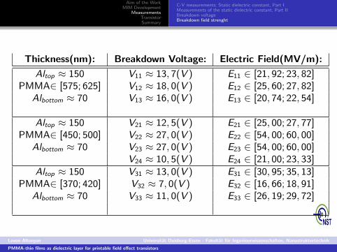
Thickness(nm): Breakdown Voltage: Electric Field(MV/m):
Altop ≈ 150 V11 ≈ 13, 7(V ) E11 ∈ [21, 92; 23, 82]PMMA∈ [575; 625] V12 ≈ 18, 0(V ) E12 ∈ [25, 60; 27, 82]
Albottom ≈ 70 V13 ≈ 16, 0(V ) E13 ∈ [20, 74; 22, 54]
Altop ≈ 150 V21 ≈ 12, 5(V ) E21 ∈ [25, 00; 27, 77]PMMA∈ [450; 500] V22 ≈ 27, 0(V ) E22 ∈ [54, 00; 60, 00]
Albottom ≈ 70 V23 ≈ 27, 0(V ) E23 ∈ [54, 00; 60, 00]V24 ≈ 10, 5(V ) E24 ∈ [21, 00; 23, 33]
Altop ≈ 150 V31 ≈ 13, 0(V ) E31 ∈ [30, 95; 35, 13]PMMA∈ [370; 420] V32 ≈ 7, 0(V ) E32 ∈ [16, 66; 18, 91]
Albottom ≈ 70 V33 ≈ 11, 0(V ) E33 ∈ [26, 19; 29, 72]
Levon Altunyan Universitat Duisburg-Essen - Fakultat fur Ingenieurwissenschaften, Nanostrukturtechnik
PMMA-thin films as dielectric layer for printable field effect transistors

Aim of the WorkMIM Development
MeasurementsTransistorSummary
C-V measurements; Static dielectric constant, Part IMeasurements of the static dielectric constant, Part IIBreakdown voltageBreakdown field strenght
Breakdown Field Strenght, Results and Discussion
Results
Majority of values are in the range between 25 to 30 (MV/m).
The critical field strength ranges correspond to the typical for polymers [6].
Ecrit ≈ 34, 73 (MV/m) fits exactly to values reported in literature [8, 9].
Levon Altunyan Universitat Duisburg-Essen - Fakultat fur Ingenieurwissenschaften, Nanostrukturtechnik
PMMA-thin films as dielectric layer for printable field effect transistors

Aim of the WorkMIM Development
MeasurementsTransistorSummary
MISFET devices
SubstrateGate ContactInsulator
Semiconductor
Source
WL Drain
UD
UGGate
Drain ContactSource Contact
GlassAl
PMMA
AlC60
Al
0 10 20 30 40−5
0
5
10
15x 10−6
VDS
[V] →
I D [A
] →
Vg=0[V]
Vg=10[V]
Vg=20[V]
Vg=30[V]
Vg=40[V]
0 10 20 30 40−5
0
5
10
15x 10−6
VDS
[V] →
I D [A
] →
Vg=0[V]
Vg=40[V]
Figure: Al/PMMA/C60/Al MISFET Structure; Characteristic Curves
Levon Altunyan Universitat Duisburg-Essen - Fakultat fur Ingenieurwissenschaften, Nanostrukturtechnik
PMMA-thin films as dielectric layer for printable field effect transistors

Aim of the WorkMIM Development
MeasurementsTransistorSummary
MISFET devices
SubstrateGate ContactInsulator
Semiconductor
Source
WL Drain
UD
UGGate
Drain ContactSource Contact
GlassAl
PMMA
Al AlPentacene
−40 −30 −20 −10 0−8
−6
−4
−2
0
2
I D [n
A] →
VDS
[V] →
Vg=0[V]
Vg=−10[V]
Vg=−20[V]
Vg=−30[V]
Vg=−40[V]
−60 −50 −40 −30 −20 −10 0−400
−300
−200
−100
0
100
VDS
[V] →
I D [n
A] →
Vg=0[V]
Vg=−10[V]
Vg=−20[V]
Vg=−30[V]
Vg=−40[V]
Vg=−50[V]
Vg=−60[V]
Figure: Al/PMMA/C60/Al MISFET Structure; Characteristic Curves
Levon Altunyan Universitat Duisburg-Essen - Fakultat fur Ingenieurwissenschaften, Nanostrukturtechnik
PMMA-thin films as dielectric layer for printable field effect transistors

Aim of the WorkMIM Development
MeasurementsTransistorSummary
MISFET devices
MISFET, Results and Discussion I
Results:
C60 n-type; pentacene’s p-type behaviour.
Some field effect is noticed.
Capacitance and a respective dielectric constant (εPMMA), similar to silicon dioxide’s, hasbeen measured. Therefore, it can be concluded that PMMA is a suitable gate dielectricfor MISFET structures, but additional studies for the reasons causing the observedcharacteristic behaviour should be carried out.
Levon Altunyan Universitat Duisburg-Essen - Fakultat fur Ingenieurwissenschaften, Nanostrukturtechnik
PMMA-thin films as dielectric layer for printable field effect transistors

Aim of the WorkMIM Development
MeasurementsTransistorSummary
MISFET devices
MISFET, Results and Discussion II
a.)
stable threshold shifts, e.g., induced by polarization of aferroelectric gate dielectric, can beused in organic memorydevices.51,52
Another important parameter of FETsthat can beextractedfrom the transfer characteristics is the on/off ratio, which isthe ratio of the drain current in the on-state at a particulargate voltage and the drain current in the off-state (Ion/Ioff).For clean switching behavior of the transistor, this valueshould be as large as possible. In situations where contactresistance effects at the source- drain electrodes can beneglected, theon-current mainly dependson themobility ofthesemiconductor and thecapacitanceof thegatedielectric.The magnitude of the off-current is determined by gateleakage, especially for unpatterned gate electrodes andsemiconductor layers, by the conduction pathways at thesubstrate interface, and by the bulk conductivity of thesemiconductor, which can increase due to unintentionaldoping, as for exampleoften observed in P3HT transistors.53- 55
2.3. Device StructuresThe physical nature of the semiconductor as well as the
employed gate dielectric may require or enable differentdevice structures that can show very different transistorbehavior. The most commonly found structures (in relationto the substrate) are the bottom contact/top gate (BC/TG,Figure4a), bottom contact/bottom gate (BC/BG, Figure4b),and top contact/bottom gate (TC/BG, Figure 4c) structures.Transistors with the same components but different geom-etries can show very dissimilar behavior.
One of the major differences between these devicegeometriesarises from theposition of the injecting electrodesin relation to the gate. In the bottom contact/bottom gatestructure, charges are directly injected into the channel ofaccumulated charges at the semiconductor- dielectric inter-face. In theother two structures, the source/drain electrodesand the channel are separated by the semiconducting layer.Thus, charges first have to travel through several tens of
nanometersof undoped semiconductor before they reach thechannel. However, in the staggered BC/TG and TC/BGconfigurations, charges are injected not only from the edgeof the electrode but also from those parts of the electrodethat overlap with the gate electrode, contributing to thecurrent depending on distance from the edge (currentcrowding).56- 58
Other differencesbetween transistor structuresarise fromthe dielectric/semiconductor and electrode/semiconductorinterfaces, such as different morphologies at the top andbottom surfaces of a semiconductor film (molecular orienta-tion, roughness)59 or introduction of trap statesduring metalevaporation on organic semiconductors for top contacttransistors.60,61
2.4. Charge Transport Models
The exact nature of charge transport in organic semicon-ductors is still open to debate. Nevertheless, one can makea clear distinction between disordered semiconductors suchas amorphous polymers and highly ordered organic singlecrystals, at the opposite ends of the spectrum. Chargetransport in disordered semiconductors isgenerally describedby thermally activated hopping of charges through adistribu-tion of localized states or shallow traps. Bassler et al. havedescribed this density of states as aGaussian distribution inorder to model chargetransport in time-of-flight experiments.The width of the Gaussian density of states is determinedby thespatial and energetic disorder within thesemiconductorand can be determined by temperature-dependent mobilitymeasurements.62 A broader density of states leads to lowermobilities and a stronger temperature dependence.
A variable range hopping model, where charges can hopa short distance with a high activation energy or a longdistance with a low activation energy, was used by Vissen-berg and Matters.63 They further assumed an exponentialdistribution of localized states, which represents the tail ofa Gaussian density of states, that dominates the transportcharacteristics at low carrier concentrations. The Vissen-berg- Matters model predicts an increase of the field-effectmobility with increasing gate voltage, as the accumulatedcharge carriers fill the lower-lying states of the organicsemiconductor first and any additional charges in theaccumulation layer will occupy states at relatively highenergies. Thus, additional charges will require a lower
Figure3. Representativecurrent- voltagecharacteristicsof an n-channel organic field-effect transistor: (a) output characteristics indicatingthe linear and saturation regimes; (b) transfer characteristics in the linear regime (Vd , Vg), indicating the onset voltage (Von) when thedrain current increases abruptly; (c) transfer characteristics in the saturation regime (Vds > Vg - VTh), indicating the threshold voltageVTh,where the linear fit to the square root of the drain current intersects with the x-axis.
Figure 4. Common field-effect transistor configurations: (a)bottom contact, top gate (BC/TG); (b) bottom contact, bottom gate(BC/BG); (c) top contact, bottom gate (TC/BG).
1300 Chemical Reviews, 2007, Vol. 107, No. 4 Zaumseil and Sirringhaus
b.)
stable threshold shifts, e.g., induced by polarization of aferroelectric gate dielectric, can beused in organic memorydevices.51,52
Another important parameter of FETsthat can beextractedfrom the transfer characteristics is the on/off ratio, which isthe ratio of the drain current in the on-state at a particulargate voltage and the drain current in the off-state (Ion/Ioff).For clean switching behavior of the transistor, this valueshould be as large as possible. In situations where contactresistance effects at the source- drain electrodes can beneglected, theon-current mainly dependson themobility ofthesemiconductor and thecapacitanceof thegatedielectric.The magnitude of the off-current is determined by gateleakage, especially for unpatterned gate electrodes andsemiconductor layers, by the conduction pathways at thesubstrate interface, and by the bulk conductivity of thesemiconductor, which can increase due to unintentionaldoping, as for exampleoften observed in P3HT transistors.53- 55
2.3. Device StructuresThe physical nature of the semiconductor as well as the
employed gate dielectric may require or enable differentdevice structures that can show very different transistorbehavior. The most commonly found structures (in relationto the substrate) are the bottom contact/top gate (BC/TG,Figure4a), bottom contact/bottom gate (BC/BG, Figure4b),and top contact/bottom gate (TC/BG, Figure 4c) structures.Transistors with the same components but different geom-etries can show very dissimilar behavior.
One of the major differences between these devicegeometriesarises from theposition of the injecting electrodesin relation to the gate. In the bottom contact/bottom gatestructure, charges are directly injected into the channel ofaccumulated charges at the semiconductor- dielectric inter-face. In theother two structures, the source/drain electrodesand the channel are separated by the semiconducting layer.Thus, charges first have to travel through several tens of
nanometersof undoped semiconductor before they reach thechannel. However, in the staggered BC/TG and TC/BGconfigurations, charges are injected not only from the edgeof the electrode but also from those parts of the electrodethat overlap with the gate electrode, contributing to thecurrent depending on distance from the edge (currentcrowding).56- 58
Other differencesbetween transistor structuresarise fromthe dielectric/semiconductor and electrode/semiconductorinterfaces, such as different morphologies at the top andbottom surfaces of a semiconductor film (molecular orienta-tion, roughness)59 or introduction of trap statesduring metalevaporation on organic semiconductors for top contacttransistors.60,61
2.4. Charge Transport Models
The exact nature of charge transport in organic semicon-ductors is still open to debate. Nevertheless, one can makea clear distinction between disordered semiconductors suchas amorphous polymers and highly ordered organic singlecrystals, at the opposite ends of the spectrum. Chargetransport in disordered semiconductors isgenerally describedby thermally activated hopping of charges through adistribu-tion of localized states or shallow traps. Bassler et al. havedescribed this density of states as aGaussian distribution inorder to model chargetransport in time-of-flight experiments.The width of the Gaussian density of states is determinedby thespatial and energetic disorder within thesemiconductorand can be determined by temperature-dependent mobilitymeasurements.62 A broader density of states leads to lowermobilities and a stronger temperature dependence.
A variable range hopping model, where charges can hopa short distance with a high activation energy or a longdistance with a low activation energy, was used by Vissen-berg and Matters.63 They further assumed an exponentialdistribution of localized states, which represents the tail ofa Gaussian density of states, that dominates the transportcharacteristics at low carrier concentrations. The Vissen-berg- Matters model predicts an increase of the field-effectmobility with increasing gate voltage, as the accumulatedcharge carriers fill the lower-lying states of the organicsemiconductor first and any additional charges in theaccumulation layer will occupy states at relatively highenergies. Thus, additional charges will require a lower
Figure3. Representativecurrent- voltagecharacteristicsof an n-channel organic field-effect transistor: (a) output characteristics indicatingthe linear and saturation regimes; (b) transfer characteristics in the linear regime (Vd , Vg), indicating the onset voltage (Von) when thedrain current increases abruptly; (c) transfer characteristics in the saturation regime (Vds > Vg - VTh), indicating the threshold voltageVTh,where the linear fit to the square root of the drain current intersects with the x-axis.
Figure 4. Common field-effect transistor configurations: (a)bottom contact, top gate (BC/TG); (b) bottom contact, bottom gate(BC/BG); (c) top contact, bottom gate (TC/BG).
1300 Chemical Reviews, 2007, Vol. 107, No. 4 Zaumseil and Sirringhaus
Figure: Common FET Configurations
Results:
It is important that the roughness of the channel interface is additionally examined.Moreover, implementation of the structures a.) bottom contact/top gate and b.) bottomcontact/bottom gate could be a more beneficial choice with respect to the materials inuse.
Lower channel roughness, increased gate voltage effect
Levon Altunyan Universitat Duisburg-Essen - Fakultat fur Ingenieurwissenschaften, Nanostrukturtechnik
PMMA-thin films as dielectric layer for printable field effect transistors

Aim of the WorkMIM Development
MeasurementsTransistorSummary
ResultsFuture Work
Summary
Summary
The spin process is optimized.
Several structures are realized.
Current leackage problem is solved.
A mask with variable area for capacitance measurements has been designed.
C-V measurements are carried out.
Estimation of dielectric constant ε is achieved.
Breakdown voltage and breakdown field strenght are studied.
An attempt to realize MISFET structures utilizing PMMA as gate dielectric is made.
The characteristic curves of the designed devices are examined.
Levon Altunyan Universitat Duisburg-Essen - Fakultat fur Ingenieurwissenschaften, Nanostrukturtechnik
PMMA-thin films as dielectric layer for printable field effect transistors

Aim of the WorkMIM Development
MeasurementsTransistorSummary
ResultsFuture Work
Proposals for Future Work
Capacitance measurements could be done on the MIS structures.
Implementation of bottom contact/bottom gate or bottom contact/top gatestructure.
Further investigation of the field effect dependence.
Levon Altunyan Universitat Duisburg-Essen - Fakultat fur Ingenieurwissenschaften, Nanostrukturtechnik
PMMA-thin films as dielectric layer for printable field effect transistors

ReferencesAbbreviations
C. LawrenceThe mechanics of spin coating of polymer films.Phys. Fluids, 31(10):2786, 1988.
Boedeker Plastics, Inc.http : //www .boedeker .com/acryl p.htmAccessed 08.03.2009.
J. Kronjaeger.Electrical properties of Insulators.http : //www .kronjaeger .com/hv − old/hv/tbl/prop.html , Accessed 08.03.2009.
N. Friction, S. Kuehn, J. Marohn and R. Loring.Noncontact Dielectric Friction.J. Phys. Chem. B, 14525 - 14528, 110, 30, 2006.
S. Gross, D. Camozzo, V. Di Noto, L. Armelao and E. Tondello.PMMA: A key macromolecular component for dielectric low-kappa hybridinorganic-organic polymer films.Eur. Polym. J., 43, 3, 2007.
Levon Altunyan Universitat Duisburg-Essen - Fakultat fur Ingenieurwissenschaften, Nanostrukturtechnik
PMMA-thin films as dielectric layer for printable field effect transistors

ReferencesAbbreviations
H. Foll.Electronic Materials - Skript.University of Kiel, Faculty of Engineering,http : //www .tf .uni − kiel .de/matwis/amat/elmat en/index .html , Accessed28.March 2009.
K. Miyairi and E. Itoh.AC Electrical Breakdown and Conduction in PMMA Thin Films and the Influence ofLiC104 as an Ionic Impurity.International Conference on Solid Dielectrics, Toidorrse, France, July 5-9, 2004.
Evonik Industries.PLEXIGLASB R© GS / PLEXIGLASB R© XT.http : //www .plexiglas.de/NR/rdonlyres/5FDB46EB − 8AB7− 486C − AC14−448B2D893034/0/2111PLEXIGLASGS XT en.pdf , July 2008, Accessed 28.March2009.
Levon Altunyan Universitat Duisburg-Essen - Fakultat fur Ingenieurwissenschaften, Nanostrukturtechnik
PMMA-thin films as dielectric layer for printable field effect transistors

ReferencesAbbreviations
Wikipedia - Die freie Enzyklopadie.Polymethylmethacrylat, Aufbau und Eigenschaften.http : //de.wikipedia.org/wiki/PlexiglasAufbau und Eigenschaften, Lastmodification 19. February 2009, Accessed on 28.March 2009
Levon Altunyan Universitat Duisburg-Essen - Fakultat fur Ingenieurwissenschaften, Nanostrukturtechnik
PMMA-thin films as dielectric layer for printable field effect transistors

ReferencesAbbreviations
Explanation of Different Abbreviations
Metal Insulator-Metal.Poly Methyl Metha AcrylateIndium Tin-Oxide.Field Effect-Transistor.Metal Insulator-Semiconductor.Metal Insulator-Semiconductor Field Effect-Transistor.Organic Field Effect-Transistor.
Table: Explanation of what different abbreviations mean.
Levon Altunyan Universitat Duisburg-Essen - Fakultat fur Ingenieurwissenschaften, Nanostrukturtechnik
PMMA-thin films as dielectric layer for printable field effect transistors