backplane high level design concept - lamsim...
TRANSCRIPT

Backplane Architecture High Level Design Example
Bert Simonovich
Issue: 1.0
Jan 24, 2011

Bert SimonovichCopyright LAMSIM Enterprises inc.2
Record of Release
1. Jan 24, 2011: Issue 1.0 - Initial Release.
Bert SimonovichCopyright LAMSIM Enterprises inc.3
Summary and Caveats
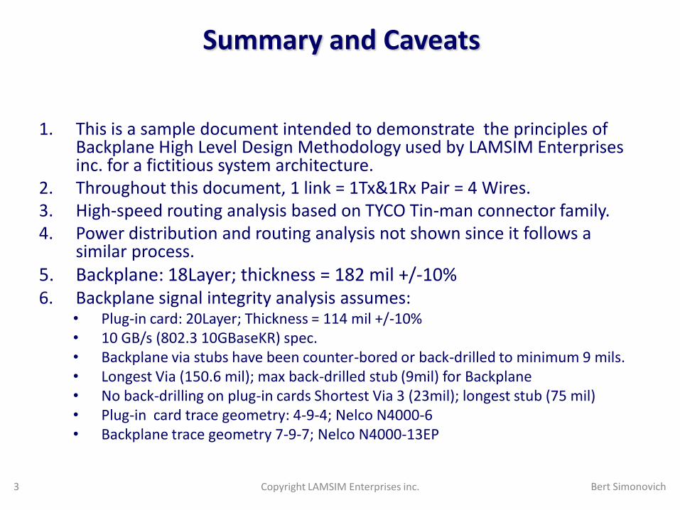
1. This is a sample document intended to demonstrate the principles of Backplane High Level Design Methodology used by LAMSIM Enterprises inc. for a fictitious system architecture.
2. Throughout this document, 1 link = 1Tx&1Rx Pair = 4 Wires.3. High-speed routing analysis based on TYCO Tin-man connector family.4. Power distribution and routing analysis not shown since it follows a
similar process.5. Backplane: 18Layer; thickness = 182 mil +/-10% 6. Backplane signal integrity analysis assumes:
• Plug-in card: 20Layer; Thickness = 114 mil +/-10% • 10 GB/s (802.3 10GBaseKR) spec.• Backplane via stubs have been counter-bored or back-drilled to minimum 9 mils. • Longest Via (150.6 mil); max back-drilled stub (9mil) for Backplane• No back-drilling on plug-in cards Shortest Via 3 (23mil); longest stub (75 mil)• Plug-in card trace geometry: 4-9-4; Nelco N4000-6• Backplane trace geometry 7-9-7; Nelco N4000-13EP
Bert SimonovichCopyright LAMSIM Enterprises inc.4
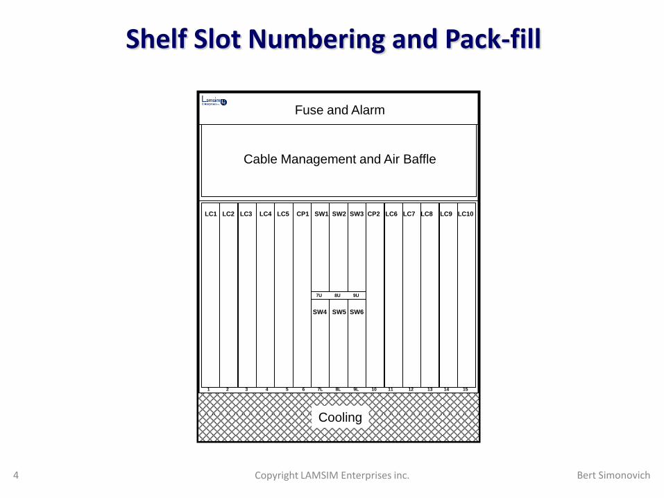
Shelf Slot Numbering and Pack-fill
7U 8U 9U
LC1 LC2 LC3 LC4 LC5 CP1 SW1 SW2 SW3 CP2 LC6 LC7 LC8 LC9 LC10
SW4 SW5 SW6
1 2 3 4 5 6 7L 8L 9L 10 11 12 13 14 15
Fuse and Alarm
Cable Management and Air Baffle
Cooling
Bert SimonovichCopyright LAMSIM Enterprises inc.5
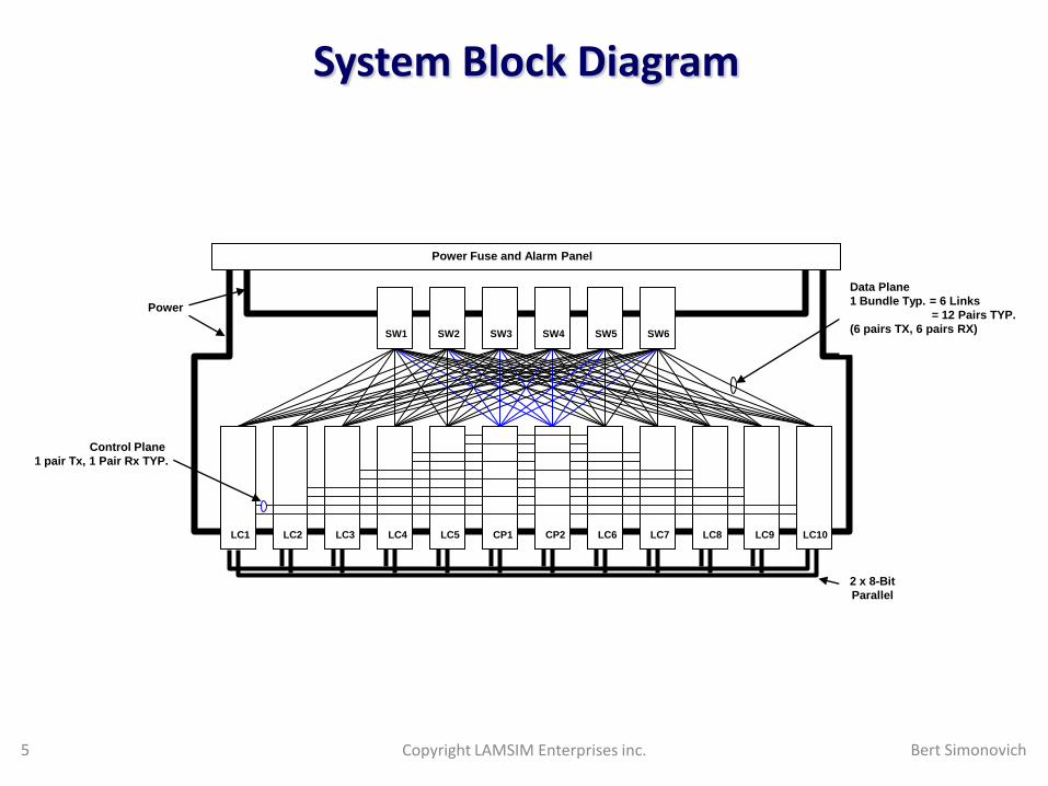
System Block Diagram
SW1 SW2 SW3 SW4 SW5 SW6
LC7 LC8 LC9 LC10LC6LC5LC4LC3LC2LC1 CP1 CP2
Power Fuse and Alarm Panel
Data Plane
1 Bundle Typ. = 6 Links
= 12 Pairs TYP.
(6 pairs TX, 6 pairs RX)
Control Plane
1 pair Tx, 1 Pair Rx TYP.
Power
2 x 8-Bit
Parallel
Bert SimonovichCopyright LAMSIM Enterprises inc.6
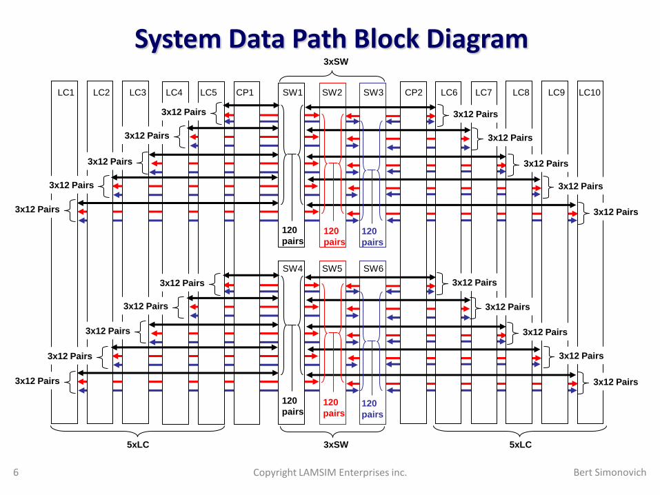
System Data Path Block Diagram
3xSW
LC10LC9LC8LC7LC6CP2CP1LC5LC4LC3LC2LC1 SW1 SW2 SW3
3x12 Pairs
3x12 Pairs
120
pairs
120
pairs120
pairs120
pairs
120
pairs
120
pairs
5xLC 5xLC
3x12 Pairs
3x12 Pairs
3x12 Pairs
3x12 Pairs
3x12 Pairs
3x12 Pairs
3x12 Pairs
3x12 Pairs
SW4 SW5 SW6
3xSW
3x12 Pairs
3x12 Pairs
3x12 Pairs
3x12 Pairs
3x12 Pairs
3x12 Pairs
3x12 Pairs
3x12 Pairs
3x12 Pairs
3x12 Pairs

Bert SimonovichCopyright LAMSIM Enterprises inc.7
System Control Path Block Diagram - GigE
3xSW
LC10LC9LC8LC7LC6CP2CP1LC5LC4LC3LC2LC1 SW1 SW2 SW3
5xLC 5xLC
SW4 SW5 SW6
3x2 Pairs
3x2 Pairs
20
Pairs
20
Pairs
2x8-Bit
Bus
3xSW
Bert SimonovichCopyright LAMSIM Enterprises inc.8
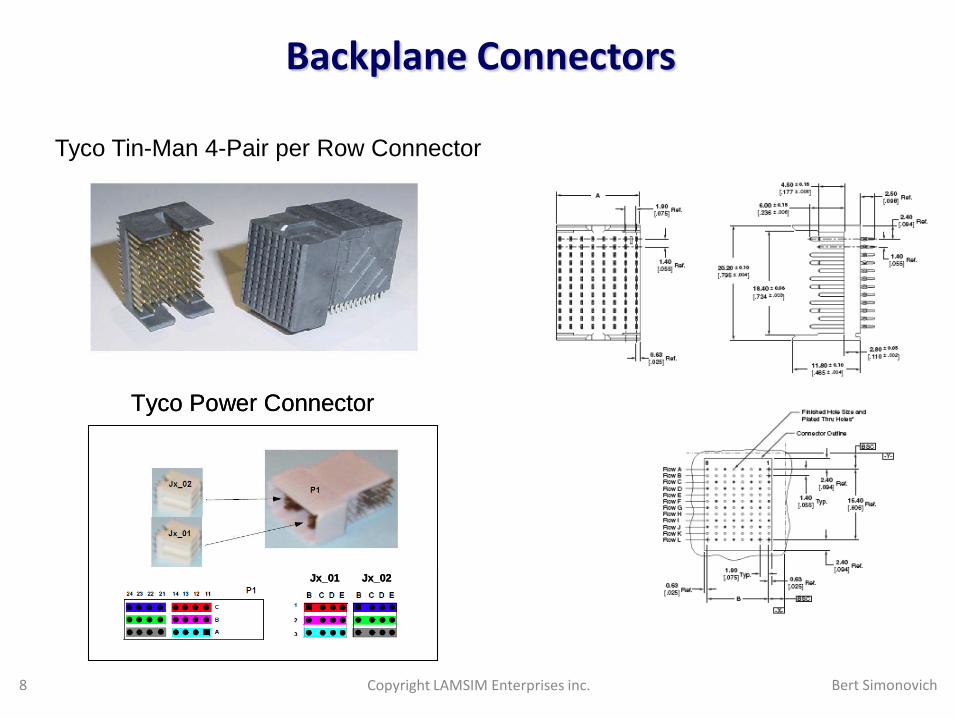
Backplane Connectors
Tyco Tin-Man 4-Pair per Row Connector
Tyco Power Connector
Jx_01 Jx_02
Tyco Power Connector
Jx_01 Jx_02
Bert SimonovichCopyright LAMSIM Enterprises inc.9
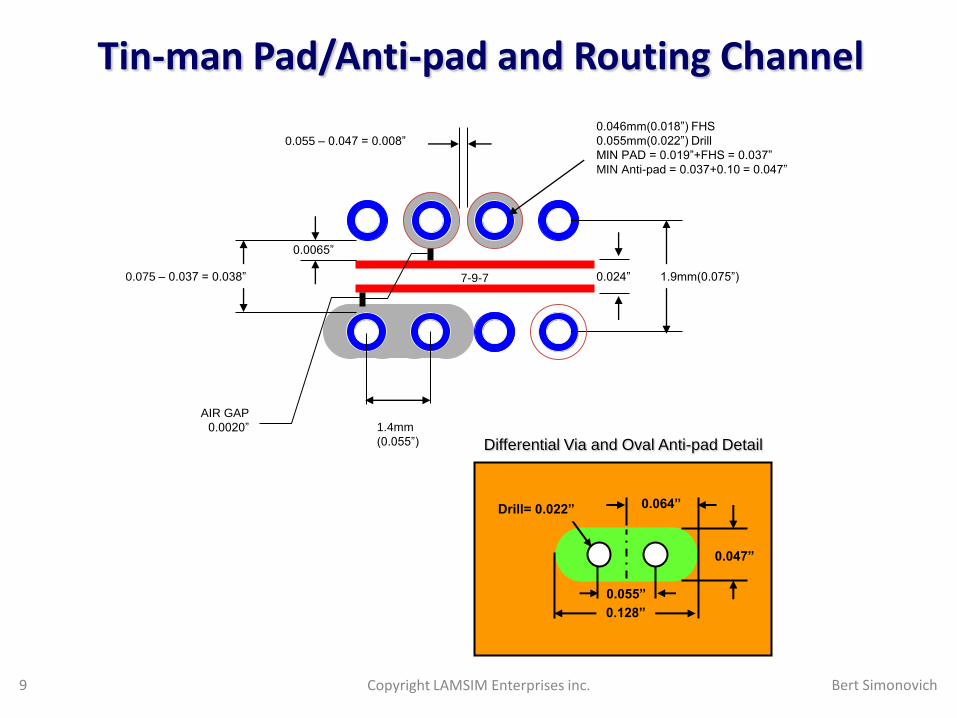
Tin-man Pad/Anti-pad and Routing Channel
7-9-7 1.9mm(0.075”)0.024”
0.046mm(0.018”) FHS
0.055mm(0.022”) Drill
MIN PAD = 0.019”+FHS = 0.037”
MIN Anti-pad = 0.037+0.10 = 0.047”
0.075 – 0.037 = 0.038”
0.0065”
1.4mm
(0.055”)
0.055 – 0.047 = 0.008”
AIR GAP
0.0020”
0.128”
0.047”
0.064”Drill= 0.022”
0.055”
Differential Via and Oval Anti-pad Detail
Bert SimonovichCopyright LAMSIM Enterprises inc.10
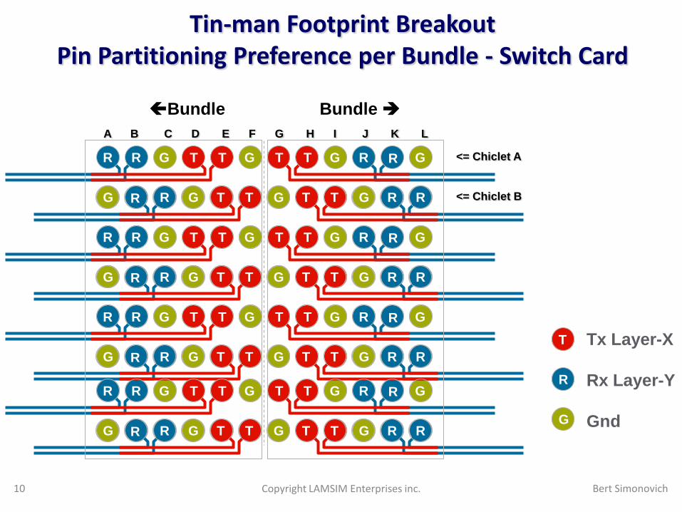
Tx Layer-X
Rx Layer-Y
Gnd
Bundle Bundle
R
T
G
RRTTTTRR G G GG
R R T T T T R RGGG G
R R T T T T R RGGG G
R R T T T T R RGGG G
R R T T T T R RGGG G
RRTTTTRR G G GG
RRTTTTRR G G GG
RRTTTTRR G G GG
<= Chiclet A
<= Chiclet B
A B C D E F G H I J K L
Tin-man Footprint Breakout Pin Partitioning Preference per Bundle - Switch Card

Bert SimonovichCopyright LAMSIM Enterprises inc.11
ETSI (ETS 300 119-4: January 1994)
Bert SimonovichCopyright LAMSIM Enterprises inc.12
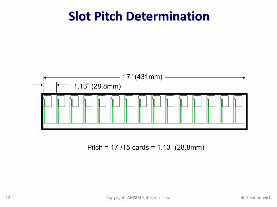
Slot Pitch Determination
Pitch = 17”/15 cards = 1.13” (28.8mm)
17” (431mm)
1.13” (28.8mm)
Bert SimonovichCopyright LAMSIM Enterprises inc.13
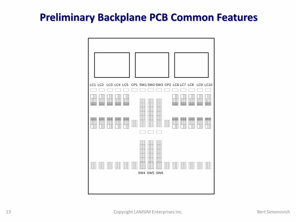
Preliminary Backplane PCB Common Features
LC1 LC2 LC3 LC4 LC5 CP1 SW1 SW2 SW3 CP2 LC6 LC7 LC8 LC9 LC10
SW4 SW5 SW6
Bert SimonovichCopyright LAMSIM Enterprises inc.14
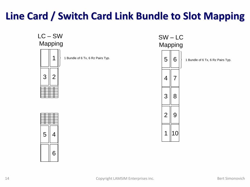
Line Card / Switch Card Link Bundle to Slot Mapping
1
23
6
45
LC – SW
Mapping
1 Bundle of 6 Tx, 6 Rz Pairs Typ.
SW – LC
Mapping
1 10
5 6
74
3 8
92
1 Bundle of 6 Tx, 6 Rz Pairs Typ.

Bert SimonovichCopyright LAMSIM Enterprises inc.15
Card Size and Connector Signal PartitioningLC CP
SW
Power Power
Power
HS Serial Links
Data Path
HS Serial Links
Data Path
HS Serial Links
Data Path
GigE Control Path
8-Bit Maintenance Bus
Configuration Bits
GigE Control Path
8-Bit Maintenance Bus
Configuration Bits
GigE Control Path
GigE Control Path
Configuration Bits
Configuration Bits
1.13”
(28.8mm)
12”
(30.5mm)
5.5”
(14mm)
1.13”
(28.8mm)
Bert SimonovichCopyright LAMSIM Enterprises inc.16
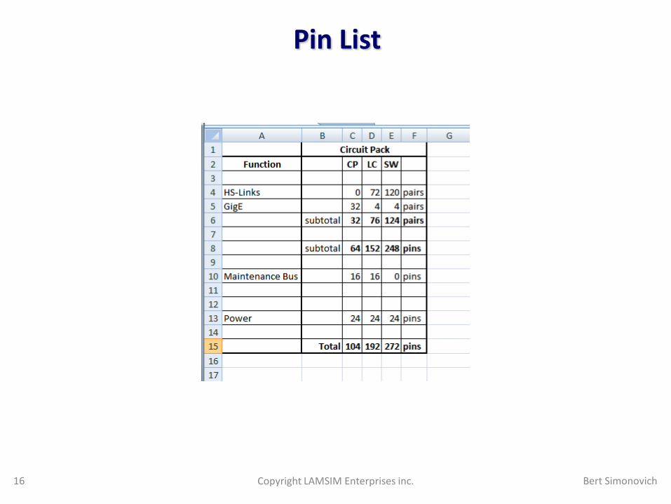
Pin List
Bert SimonovichCopyright LAMSIM Enterprises inc.17
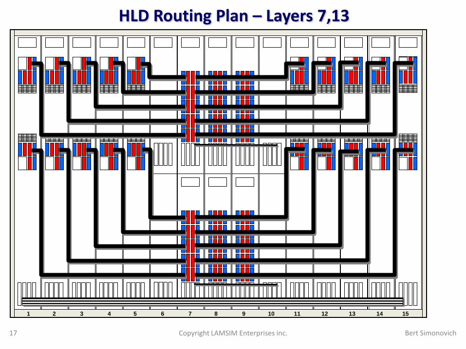
1 2 3 4 5 6 7 8 9 10 11 12 13 14 15
HLD Routing Plan – Layers 7,13

Bert SimonovichCopyright LAMSIM Enterprises inc.18
1 2 3 4 5 6 7 8 9 10 11 12 13 14 15
HLD Routing Plan – Layers 9,15
Bert SimonovichCopyright LAMSIM Enterprises inc.19
1 2 3 4 5 6 7 8 9 10 11 12 13 14 15
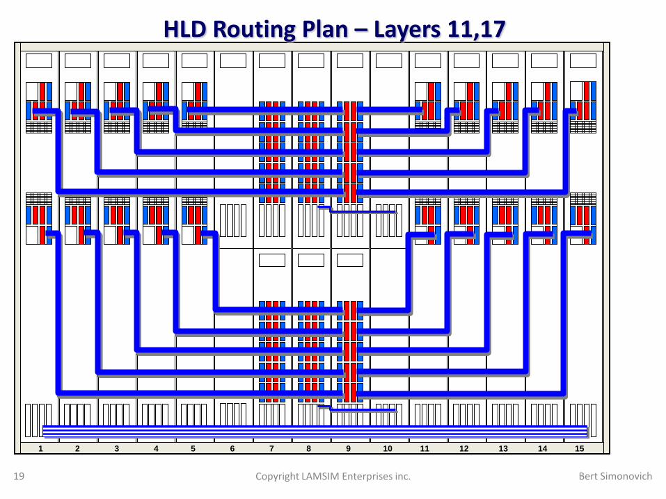
HLD Routing Plan – Layers 11,17
Bert SimonovichCopyright LAMSIM Enterprises inc.20
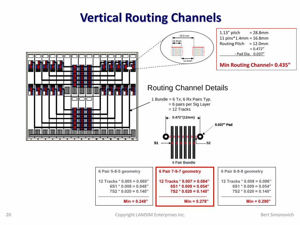
Vertical Routing Channels1.13” pitch = 28.8mm11 pins*1.4mm = 16.8mmRouting Pitch = 12.0mm
= 0.472”- Pad Dia. 0.037”
Min Routing Channel= 0.435”
16.8mm
28.8 mm
12.0mm
Routing Channel Details
1 Bundle = 6 Tx; 6 Rx Pairs Typ.
= 6 pairs per Sig Layer
= 12 Tracks
6 Pair 5-8-5 geometry
12 Tracks * 0.005 = 0.060”
6S1 * 0.008 = 0.048”
7S2 * 0.020 = 0.140”
------------------------------------
Min = 0.248”
6 Pair 7-9-7 geometry
12 Tracks * 0.007 = 0.084”
6S1 * 0.009 = 0.054”
7S2 * 0.020 = 0.140”
----------------------------------
Min = 0.278”
0.037” Pad
0.472”(12mm)
S2S1
0.037” Pad
0.472”(12mm)
S2S1
6 Pair 8-9-8 geometry
12 Tracks * 0.008 = 0.096”
6S1 * 0.009 = 0.054”
7S2 * 0.020 = 0.140”
------------------------------------
Min = 0.290”
Bert SimonovichCopyright LAMSIM Enterprises inc.21
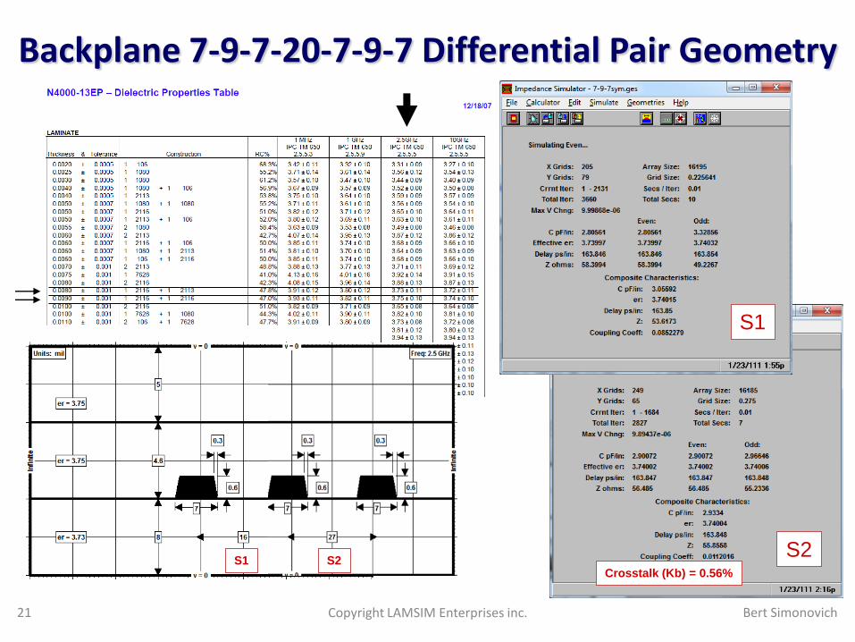
Backplane 7-9-7-20-7-9-7 Differential Pair Geometry
S1 S2
S1
S2Crosstalk (Kb) = 0.56%
Bert SimonovichCopyright LAMSIM Enterprises inc.22
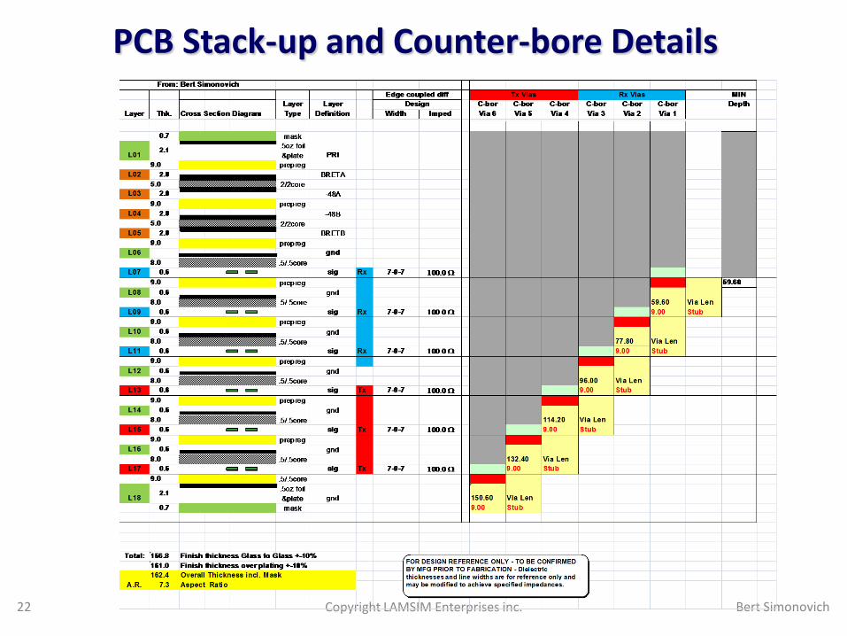
PCB Stack-up and Counter-bore Details
Bert SimonovichCopyright LAMSIM Enterprises inc.23
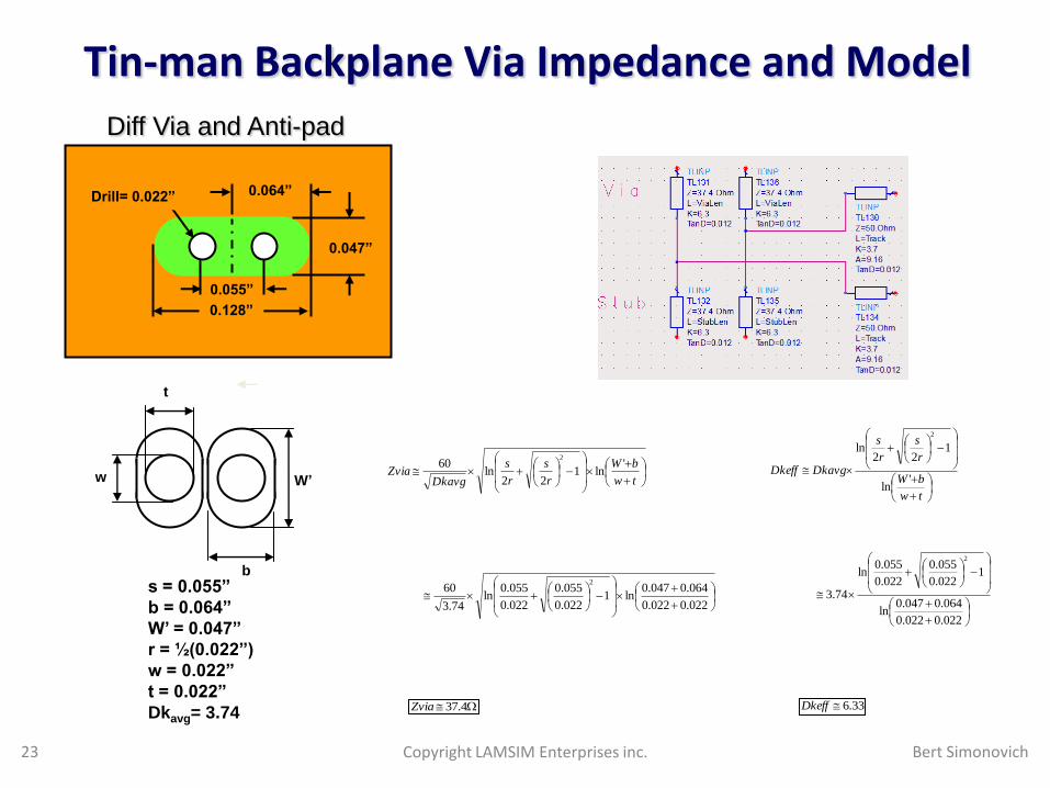
Tin-man Backplane Via Impedance and Model
t
W’
b
w
s = 0.055”
b = 0.064”
W’ = 0.047”
r = ½(0.022”)
w = 0.022”
t = 0.022”
Dkavg= 3.74
tw
bW
r
s
r
s
DkavgZvia
'ln1
22ln
602
022.0022.0
064.0047.0ln1
022.0
055.0
022.0
055.0ln
74.3
602
4.37Zvia
tw
bW
r
s
r
s
DkavgDkeff'
ln
122
ln
2
022.0022.0
064.0047.0ln
1022.0
055.0
022.0
055.0ln
74.3
2
33.6Dkeff
0.128”
0.047”
0.064”Drill= 0.022”
0.055”
Diff Via and Anti-pad
Bert SimonovichCopyright LAMSIM Enterprises inc.24
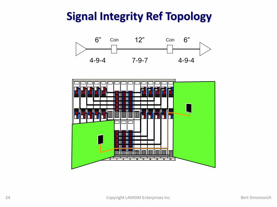
Signal Integrity Ref Topology
12”6” 6”
7-9-74-9-4 4-9-4
Con Con
Bert SimonovichCopyright LAMSIM Enterprises inc.25
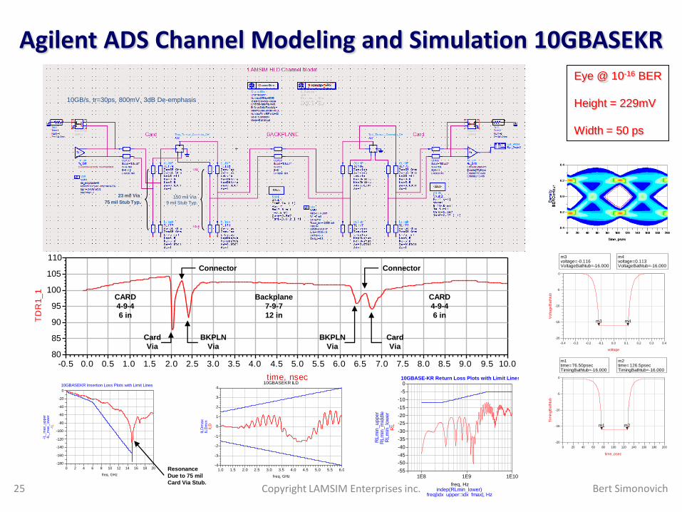
Agilent ADS Channel Modeling and Simulation 10GBASEKR
1E91E8 1E10
-50
-45
-40
-35
-30
-25
-20
-15
-10
-5
-55
0
freq, Hz
RL
indep(RLmin_lower)
RLm
in_lo
wer
RLm
in_m
iddle
freq[idx_upper::idx_fmax], Hz
RLm
in_upper
10GBASE-KR Return Loss Plots with Limit Lines
0.0 0.5 1.0 1.5 2.0 2.5 3.0 3.5 4.0 4.5 5.0 5.5 6.0 6.5 7.0 7.5 8.0 8.5 9.0 9.5-0.5 10.0
85
90
95
100
105
80
110
time, nsec
TD
R1_1
Card
Via
Card
Via
BKPLN
Via
BKPLN
Via
Backplane
7-9-7
12 in
CARD
4-9-4
6 in
CARD
4-9-4
6 in
Connector Connector
-0.3 -0.2 -0.1 0.0 0.1 0.2 0.3-0.4 0.4
-15
-10
-5
-20
0
voltage
Vo
lta
ge
Ba
thtu
b
-0.116-16.000
m3
0.113-16.000
m4
m3voltage=VoltageBathtub=-16.000
-0.116m4voltage=VoltageBathtub=-16.000
0.113
20 40 60 80 100 120 140 160 1800 200
-15
-10
-5
-20
0
time, psec
Tim
ing
Ba
thtu
b
76.50p-16.00
m1
126.5p-16.00
m2
m1time=TimingBathtub=-16.000
76.50psecm2time=TimingBathtub=-16.000
126.5psec
2 4 6 8 10 12 14 16 180 20
-160
-140
-120
-100
-80
-60
-40
-20
-180
0
freq, GHz
-IL
-IL_m
ax_lo
wer
-IL_m
ax_upper
10GBASEKR Insertion Loss Plots with Limit Lines
1.5 2.0 2.5 3.0 3.5 4.0 4.5 5.0 5.51.0 6.0
-3
-2
-1
0
1
2
3
-4
4
freq, GHz
ILD
ILD
min
ILD
ma
x
10GBASEKR ILD
10GB/s, tr=30ps, 800mV, 3dB De-emphasis
Eye @ 10-16 BER
Height = 229mV
Width = 50 ps
Resonance
Due to 75 mil
Card Via Stub.
150 mil Via
9 mil Stub Typ.
23 mil Via
75 mil Stub Typ.