ballistic phonon transport in holey...
TRANSCRIPT

Ballistic Phonon Transport in Holey SiliconJaeho Lee,†,§,⊥,# Jongwoo Lim,†,§,# and Peidong Yang*,†,‡,§,∥
†Department of Chemistry, ‡Department of Materials Science and Engineering, University of California, Berkeley, California 94720,United States,§Materials Sciences Division, Lawrence Berkeley National Laboratory, Berkeley, California 94720, United States,∥Kavli Energy Nanosciences Institute, Berkeley, California 94720, United States,⊥Department of Mechanical and Aerospace Engineering, University of California, Irvine, California 92697, United States
*S Supporting Information
ABSTRACT: When the size of semiconductors is smallerthan the phonon mean free path, phonons can carry heat withno internal scattering. Ballistic phonon transport has receivedattention for both theoretical and practical aspects becauseFourier’s law of heat conduction breaks down and the heatdissipation in nanoscale transistors becomes unpredictable inthe ballistic regime. While recent experiments demonstrateroom-temperature evidence of ballistic phonon transport invarious nanomaterials, the thermal conductivity data for siliconin the length scale of 10−100 nm is still not available due toexperimental challenges. Here we show ballistic phonon transport prevails in the cross-plane direction of holey silicon from 35 to200 nm. The thermal conductivity scales linearly with the length (thickness) even though the lateral dimension (neck) is asnarrow as 20 nm. We assess the impact of long-wavelength phonons and predict a transition from ballistic to diffusive regimeusing scaling models. Our results support strong persistence of long-wavelength phonons in nanostructures and are useful forcontrolling phonon transport for thermoelectrics and potential phononic applications.
KEYWORDS: Thermal conductivity, cross-plane, heat transfer, thermoelectric, nanoporous, phononic crystals
Ballistic phonon transport received large attention forfundamental interests in heat conduction across super-
lattices and nanoscale materials.1,2 When the length scale in thedirection of temperature gradient is shorter than the phononmean free path, phonons can travel through the medium withno internal scattering, which leads to absence of localtemperature or thermodynamic equilibrium. The thermalconductivity becomes a property that depends on the systemsize. The ballistic phonon transport in silicon has greatrelevance to practical applications3−7 due to the change inthermal conductivity. Thermal conductivity reduction in siliconnanostructures has been one of the major themes ofthermoelectrics in the past decade.8−15 The vapor−liquid−solid grown nanowires8−10 provided lateral spatial confinementbelow the phonon mean free path and reduced the thermalconductivity by an order of magnitude compared to bulksilicon. The crystalline nanowires with induced surfaceroughness9−13 demonstrated thermal conductivity approachingthe amorphous limit. While many versions of silicon nanowirethermal conductivity data exist, experimental reports showingthe length dependence below the phonon mean free path arenot available. The average phonon mean free path of silicon atroom temperature is known to be around 200−300 nm basedon theoretical predictions1 and thin film experiments.18 Thepast thermal conductivity measurement12 for silicon nanowiresof varying length from 3 to 50 μm did not show any appreciable
dependence because of the relatively large length scale.Thermal conductivity of silicon nanowires in submicrometerlength scales may show further reduction, which is desirable forthermoelectric applications.Ballistic phonon transport in silicon is important in
nanoelectronics because transistor length scales are activelyscaling below the phonon mean free path and the resultantthermal conductivity reduction leads to excessive heatgeneration.3,4 The ballistic phonon transport in silicon is alsoimportant for potential phononic applications, which are aimingto process information by controlling heat flow.6,7 Thephononic applications have not been explored much becauseinelastic phonon scattering is considered dominant at roomtemperature and destroys wave characteristics or informationprocessing capabilities. In other words, ballistic phonontransport at room temperature has been considered negligibleat room temperature. Only recently, novel experiments havedemonstrated strong presence of ballistic phonon transport atroom temperature through ultrafast X-ray beams,16 transientthermal gratings,17 and homogeneously alloyed nanowires.5
Chang et al.5 utilized an alloy filtering mechanism for high-frequency phonons in SiGe nanowires and successfully showed
Received: February 5, 2015Revised: March 29, 2015
Letter
pubs.acs.org/NanoLett
© XXXX American Chemical Society A DOI: 10.1021/acs.nanolett.5b00495Nano Lett. XXXX, XXX, XXX−XXX
the low frequency driven ballistic thermal conductivity in therange of 1−8 μm. However, the ballistic thermal conductivitydata for single-crystalline silicon, particularly in the length scaleof 10−100 nm, is not available despite its direct relevance tonanoscale transistors and potential phononic devices. Theexperimental demonstration of ballistic phonon transport insilicon nanostructures imposes great challenges. For siliconnanowires, the challenge lies at the MEMS device fabrication, inwhich the spatial resolution typically exceeds the phonon meanfree path. For silicon thin films, the challenge lies at themeasurement sensitivity, which is typically very low due to thelarge thermal conductivity of silicon. While the literature is richwith the thermal conductivity data for silicon thin films in thein-plane direction,18,32,33 the cross-plane thermal conductivitystill lacks length (thickness) dependence data. Here we utilizean inverse-nanowire system, i.e., holey silicon, to study ballisticphonon transport and characterize the cross-plane thermalconductivity in the length scale of 35−200 nm. Holey siliconhas very low effective thermal conductivity due to porosity and
provides substantially increased sensitivity for cross-planemeasurements. The holey silicon nanostructures have demon-strated great potential as thermoelectric materials,11,12 and ourresults showing strong ballistic phonon transport may haveimportant implications for the future of phononic applications.We fabricated holey silicon devices using highly ordered
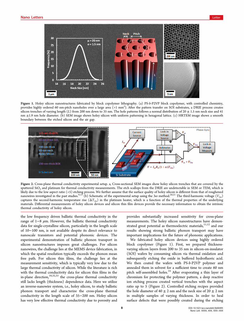
block copolymer (Figure 1). First, we prepared thickness-varying silicon layers from 200 to 35 nm in silicon-on-insulator(SOI) wafers by consuming silicon via thermal oxidation andsubsequently etching the oxide in buffered hydrofluoric acid.We then coated the wafers with PS-b-P2VP polymer andannealed them in solvent for a sufficient time to create 60 nmpitch self-assembled holes.14 After evaporating a thin layer ofchromium for protecting the polymer pattern, a deep reactiveion etching process created vertical trenches with the aspectratio up to 5 (Figure 2). Controlled etching recipes providedthe hole diameter of 40 ± 2 nm and the neck size of 20 ± 2 nmin multiple samples of varying thickness. In order to healsurface defects that were possibly created during the etching
Figure 1. Holey silicon nanostructures fabricated by block copolymer lithography. (a) PS-b-P2VP block copolymer, with controlled chemistry,provides highly ordered 60 nm-pitch nanoholes over a large area (>1 mm2). After the pattern transfer on SOI substrates, a DRIE process createssilicon trenches of varying length (L) from 200 nm down to 35 nm. The hole patterns follows a normal distribution of 20 ± 1.5 nm neck size and 41nm ±1.9 nm hole diameter. (b) SEM image shows holey silicon with uniform patterning in hexagonal lattice. (c) HRTEM image shows a smoothboundary between the etched silicon and the air gap.
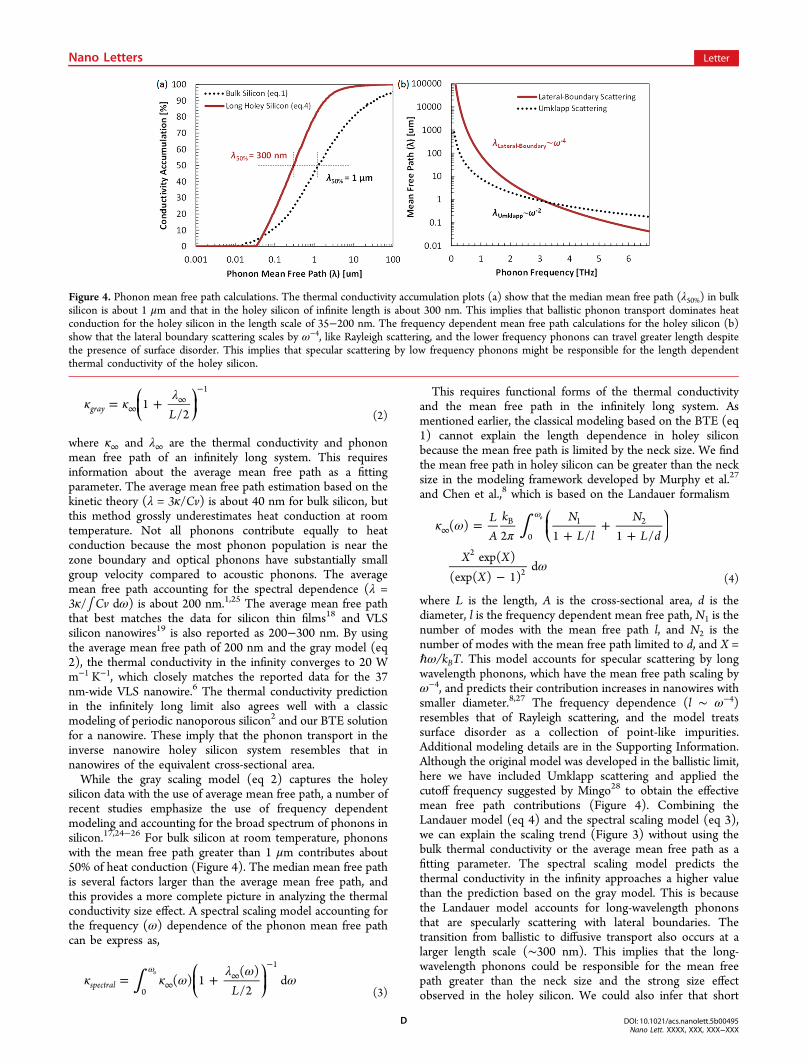
Figure 2. Cross-plane thermal conductivity experimental setup. a, Cross-sectional SEM images show holey silicon trenches that are covered by thesputtered SiO2 and platinum for thermal conductivity measurements. The etch scallops from the DRIE are undetectable in SEM or TEM, which islikely due to the low aspect ratio (<5) etching process. We further assume that the surface quality of holey silicon is different from that of roughenednanowires investigated in the past studies.9,13 (b) Schematic of the experimental setup using the 3ω method.20,21 The third-harmonic voltage (V3ω)captures the second-harmonic temperature rise (ΔT2ω) in the platinum heater, which is a function of the thermal properties of the underlyingmaterials. Differential measurements of holey silicon devices and silicon thin film devices provide the necessary information to obtain the intrinsicthermal conductivity of holey silicon.
Nano Letters Letter
DOI: 10.1021/acs.nanolett.5b00495Nano Lett. XXXX, XXX, XXX−XXX
B

process, we postannealed the samples at 800 °C in argon. Theholey silicon structures were covered by a thin film of sputteredSiO2, and then four-probe platinum electrodes were fabricatedusing a standard photolithography process. Using the platinumas a mask, we then removed the SiO2 and the holey siliconoutside the electrode area using anisotropic dry etchingprocesses. This created a one-dimensional structure on siliconsubstrate for cross-plane thermal conductivity measurements(Figure 2). Additional fabrication details are in the SupportingInformation.We characterize the cross-plane thermal conductivity of
holey silicon using the 3ω method.20,21 When a platinumelectrode transmits current at frequency ω (Iω = I0 cos(ωt)),Joule heating occurs at 2ω (Q2ω) because the heating power isIω
2R = I02R(1 + cos(2ωt))/2. Consequently, the temperature
oscillates at 2ω, and the temperature dependent electricalresistance also has a component at 2ω (R2ω). The resultantvoltage drop across the heater now contains a 3ω component(V3ω = IωR2ω). A circuitry of differential amplifiers and lock-inamplifiers captures the in-phase 3ω voltage with highsensitivity. The measured 3ω voltage is directly related to thetemperature oscillation in the platinum heater, which is afunction of thermal properties of underlying materials includingthe holey silicon layer. We fit the data to a multilayer heatconduction solution that accounts for the thermal conductivity,the anisotropy ratio, the boundary resistance, and the heatcapacity of each layer using recursive matrix formulation.21 Wemaximize the measurement sensitivity to the cross-planethermal conductivity of holey silicon by optimizing the heatingfrequency, forcing the heat conduction in one-dimensional, andminimizing the uncertainty in other materials using controldevices. The control devices are identical to holey silicondevices except for the absence of holes and provide theinformation about SiO2 layers and Si substrates for determiningthe thermal conductivity of holey silicon. This is based on theassumption that holey silicon and control devices share thesame thermal properties in the SiO2 layers and the Si substrate.The SiO2 layers are created on both holey silicon and thin filmcontrol devices simultaneously inside the same chamber, andwe assume any geometric effects such as phonon crowding arenegligible in the sputtered SiO2 because the phonon mean freepath is very small in the amorphous material. The difference inthe cross-sectional areas of holey silicon and thin film controldevices are treated with the measured porosity from the imageprocessing characterization. Another assumption is in using atheoretical thermal conductivity for silicon films in controldevices, but the uncertainty is low because the silicon films havea very small contribution (<2%) to the total resistance. Thesensitivity to holey silicon increases further when the porosity ishigher because the effective thermal resistance of holey siliconincreases compared to other materials. For porosity 30% orhigher, the uncertainty in differential analysis is 6% or lower.Additional experimental details are given in the SupportingInformation.Figure 3 shows the length dependent thermal conductivity of
holey silicon at room temperature. The thermal conductivityincreases with the length from 1.5 ± 0.2 to 2.8 ± 0.4, 3.9 ± 0.6,and 7.5 ± 1.5 W m−1 K−1 for 35 to 70, 100, and 200 nm,respectively. The reported values are the material thermalconductivity that is numerically independent of the boundaryresistance and the porosity. The porosity values ranging from20% to 40% are obtained from the image processing method.The strong length dependence indicates that ballistic phonon
transport dominates heat conduction in the cross-planedirection of holey silicon. The presence of ballistic phononsin the length scale of 35−200 nm is not surprising because thephonon mean free path in silicon can range up to severalmicrometers.25,26 It is, however, important to note that theholey silicon has lateral dimensions as narrow as 20 nm. Whileclassical models predict the smallest dimension regardless ofheat flow direction limits phonon transport, the experimentaldata suggests the length scale that is not the smallest dimensionbut in the same direction with heat flow can be important.In general, the Boltzmann transport equation (BTE) is a
great resource to understand phonon transport in semi-conductors. The thermal conductivity can be expressed inspherical coordinates as,
∫ ∫ ∫∑κπ
τ θ θ ϕ=π π
C v k k1
8sin d d d
n
k
ph g2 0 0
2
0
2 2o
(1)
where the heat capacity (Cph), group velocity (vg), andrelaxation time (τ) are each dependent on the phonondispersion relations (ω, k). The relaxation time due to cross-plane boundary scattering is L/(2 vph cos θ) where vph = ∂ω/∂k.The modeling details are in the Supporting Information. In theworst-case scenario, phonons scatter completely diffusely at thelateral boundaries and the mean free path is limited by the necksize, as if they are passing through nanowires of the diameterequivalent to the neck size. The nanowire analogy provides theclassical lower bound for the holey silicon nanostructures(Figure 3).The length dependent thermal conductivity in silicon
nanostructures, while not easily observed in experiment, hasbeen investigated by many theoretical studies.22−25 Onepopular approach is using a gray model, which has beenreported to reproduce the values from the Green−Kubocalculations22 and used to study the size effect in the thermalconductivity of silicon nanostructures.22,25 The thermalconductivity scaling in gray model can be expressed as
Figure 3. Length dependent thermal conductivity of holey silicon atroom temperature. The thermal conductivity values are numericallyindependent of the boundary resistance and the porosity. The stronglength dependence indicates that ballistic phonon transport dominatesheat conduction in the length scale of 35−200 nm. A simple scalingmodel (eq 2) using the average mean free path of bulk silicon predictsthe thermal conductivity may approach the reported nanowire data8 inthe infinitely long limit. A semiempirical model (eq 3) accounting forthe phonon spectral dependence attributes the length dependent datato the presence of long-wavelength phonons that have the mean freepath greater than the length of holey silicon nanostructures.
Nano Letters Letter
DOI: 10.1021/acs.nanolett.5b00495Nano Lett. XXXX, XXX, XXX−XXX
C
κ κλ
= +∞∞
−⎛⎝⎜
⎞⎠⎟L
1/2gray
1
(2)
where κ∞ and λ∞ are the thermal conductivity and phononmean free path of an infinitely long system. This requiresinformation about the average mean free path as a fittingparameter. The average mean free path estimation based on thekinetic theory (λ = 3κ/Cv) is about 40 nm for bulk silicon, butthis method grossly underestimates heat conduction at roomtemperature. Not all phonons contribute equally to heatconduction because the most phonon population is near thezone boundary and optical phonons have substantially smallgroup velocity compared to acoustic phonons. The averagemean free path accounting for the spectral dependence (λ =3κ/∫ Cv dω) is about 200 nm.1,25 The average mean free paththat best matches the data for silicon thin films18 and VLSsilicon nanowires19 is also reported as 200−300 nm. By usingthe average mean free path of 200 nm and the gray model (eq2), the thermal conductivity in the infinity converges to 20 Wm−1 K−1, which closely matches the reported data for the 37nm-wide VLS nanowire.6 The thermal conductivity predictionin the infinitely long limit also agrees well with a classicmodeling of periodic nanoporous silicon2 and our BTE solutionfor a nanowire. These imply that the phonon transport in theinverse nanowire holey silicon system resembles that innanowires of the equivalent cross-sectional area.While the gray scaling model (eq 2) captures the holey
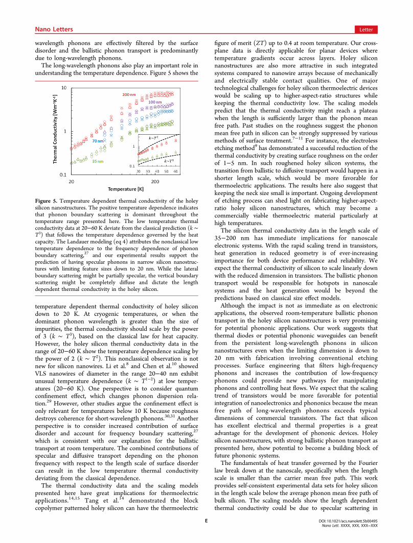
silicon data with the use of average mean free path, a number ofrecent studies emphasize the use of frequency dependentmodeling and accounting for the broad spectrum of phonons insilicon.17,24−26 For bulk silicon at room temperature, phononswith the mean free path greater than 1 μm contributes about50% of heat conduction (Figure 4). The median mean free pathis several factors larger than the average mean free path, andthis provides a more complete picture in analyzing the thermalconductivity size effect. A spectral scaling model accounting forthe frequency (ω) dependence of the phonon mean free pathcan be express as,
∫κ κ ωλ ω
ω= +ω
∞∞
−⎛⎝⎜
⎞⎠⎟L
( ) 1( )/2
dspectral0
1o
(3)
This requires functional forms of the thermal conductivityand the mean free path in the infinitely long system. Asmentioned earlier, the classical modeling based on the BTE (eq1) cannot explain the length dependence in holey siliconbecause the mean free path is limited by the neck size. We findthe mean free path in holey silicon can be greater than the necksize in the modeling framework developed by Murphy et al.27
and Chen et al.,8 which is based on the Landauer formalism
∫κ ωπ
ω
=+
++
−
ω
∞⎛⎝⎜
⎞⎠⎟
LA
k NL l
NL d
X XX
( )2 1 / 1 /
exp( )(exp( ) 1)
d
B
0
1 2
2
2
o
(4)
where L is the length, A is the cross-sectional area, d is thediameter, l is the frequency dependent mean free path, N1 is thenumber of modes with the mean free path l, and N2 is thenumber of modes with the mean free path limited to d, and X =ℏω/kBT. This model accounts for specular scattering by longwavelength phonons, which have the mean free path scaling byω−4, and predicts their contribution increases in nanowires withsmaller diameter.8,27 The frequency dependence (l ∼ ω−4)resembles that of Rayleigh scattering, and the model treatssurface disorder as a collection of point-like impurities.Additional modeling details are in the Supporting Information.Although the original model was developed in the ballistic limit,here we have included Umklapp scattering and applied thecutoff frequency suggested by Mingo28 to obtain the effectivemean free path contributions (Figure 4). Combining theLandauer model (eq 4) and the spectral scaling model (eq 3),we can explain the scaling trend (Figure 3) without using thebulk thermal conductivity or the average mean free path as afitting parameter. The spectral scaling model predicts thethermal conductivity in the infinity approaches a higher valuethan the prediction based on the gray model. This is becausethe Landauer model accounts for long-wavelength phononsthat are specularly scattering with lateral boundaries. Thetransition from ballistic to diffusive transport also occurs at alarger length scale (∼300 nm). This implies that the long-wavelength phonons could be responsible for the mean freepath greater than the neck size and the strong size effectobserved in the holey silicon. We could also infer that short
Figure 4. Phonon mean free path calculations. The thermal conductivity accumulation plots (a) show that the median mean free path (λ50%) in bulksilicon is about 1 μm and that in the holey silicon of infinite length is about 300 nm. This implies that ballistic phonon transport dominates heatconduction for the holey silicon in the length scale of 35−200 nm. The frequency dependent mean free path calculations for the holey silicon (b)show that the lateral boundary scattering scales by ω−4, like Rayleigh scattering, and the lower frequency phonons can travel greater length despitethe presence of surface disorder. This implies that specular scattering by low frequency phonons might be responsible for the length dependentthermal conductivity of the holey silicon.
Nano Letters Letter
DOI: 10.1021/acs.nanolett.5b00495Nano Lett. XXXX, XXX, XXX−XXX
D
wavelength phonons are effectively filtered by the surfacedisorder and the ballistic phonon transport is predominantlydue to long-wavelength phonons.The long-wavelength phonons also play an important role in
understanding the temperature dependence. Figure 5 shows the
temperature dependent thermal conductivity of holey silicondown to 20 K. At cryogenic temperatures, or when thedominant phonon wavelength is greater than the size ofimpurities, the thermal conductivity should scale by the powerof 3 (k ∼ T3), based on the classical law for heat capacity.However, the holey silicon thermal conductivity data in therange of 20−60 K show the temperature dependence scaling bythe power of 2 (k ∼ T2). This nonclassical observation is notnew for silicon nanowires. Li et al.8 and Chen et al.10 showedVLS nanowires of diameter in the range 20−40 nm exhibitunusual temperature dependence (k ∼ T1−2) at low temper-atures (20−60 K). One perspective is to consider quantumconfinement effect, which changes phonon dispersion rela-tion.29 However, other studies argue the confinement effect isonly relevant for temperatures below 10 K because roughnessdestroys coherence for short-wavelength phonons.30,31 Anotherperspective is to consider increased contribution of surfacedisorder and account for frequency boundary scattering,27
which is consistent with our explanation for the ballistictransport at room temperature. The combined contributions ofspecular and diffusive transport depending on the phononfrequency with respect to the length scale of surface disordercan result in the low temperature thermal conductivitydeviating from the classical dependence.The thermal conductivity data and the scaling models
presented here have great implications for thermoelectricapplications.14,15 Tang et al.14 demonstrated the blockcopolymer patterned holey silicon can have the thermoelectric
figure of merit (ZT) up to 0.4 at room temperature. Our cross-plane data is directly applicable for planar devices wheretemperature gradients occur across layers. Holey siliconnanostructures are also more attractive in such integratedsystems compared to nanowire arrays because of mechanicallyand electrically stable contact qualities. One of majortechnological challenges for holey silicon thermoelectric deviceswould be scaling up to higher-aspect-ratio structures whilekeeping the thermal conductivity low. The scaling modelspredict that the thermal conductivity might reach a plateauwhen the length is sufficiently larger than the phonon meanfree path. Past studies on the roughness suggest the phononmean free path in silicon can be strongly suppressed by variousmethods of surface treatment.7−11 For instance, the electrolessetching method9 has demonstrated a successful reduction of thethermal conductivity by creating surface roughness on the orderof 1−5 nm. In such roughened holey silicon systems, thetransition from ballistic to diffusive transport would happen in ashorter length scale, which would be more favorable forthermoelectric applications. The results here also suggest thatkeeping the neck size small is important. Ongoing developmentof etching process can shed light on fabricating higher-aspect-ratio holey silicon nanostructures, which may become acommercially viable thermoelectric material particularly athigh temperatures.The silicon thermal conductivity data in the length scale of
35−200 nm has immediate implications for nanoscaleelectronic systems. With the rapid scaling trend in transistors,heat generation in reduced geometry is of ever-increasingimportance for both device performance and reliability. Weexpect the thermal conductivity of silicon to scale linearly downwith the reduced dimension in transistors. The ballistic phonontransport would be responsible for hotspots in nanoscalesystems and the heat generation would be beyond thepredictions based on classical size effect models.Although the impact is not as immediate as on electronic
applications, the observed room-temperature ballistic phonontransport in the holey silicon nanostructures is very promisingfor potential phononic applications. Our work suggests thatthermal diodes or potential phononic waveguides can benefitfrom the persistent long-wavelength phonons in siliconnanostructures even when the limiting dimension is down to20 nm with fabrication involving conventional etchingprocesses. Surface engineering that filters high-frequencyphonons and increases the contribution of low-frequencyphonons could provide new pathways for manipulatingphonons and controlling heat flows. We expect that the scalingtrend of transistors would be more favorable for potentialintegration of nanoelectronics and phononics because the meanfree path of long-wavelength phonons exceeds typicaldimensions of commercial transistors. The fact that siliconhas excellent electrical and thermal properties is a greatadvantage for the development of phononic devices. Holeysilicon nanostructures, with strong ballistic phonon transport aspresented here, show potential to become a building block offuture phononic systems.The fundamentals of heat transfer governed by the Fourier
law break down at the nanoscale, specifically when the lengthscale is smaller than the carrier mean free path. This workprovides self-consistent experimental data sets for holey siliconin the length scale below the average phonon mean free path ofbulk silicon. The scaling models show the length dependentthermal conductivity could be due to specular scattering in
Figure 5. Temperature dependent thermal conductivity of the holeysilicon nanostructures. The positive temperature dependence indicatesthat phonon boundary scattering is dominant throughout thetemperature range presented here. The low temperature thermalconductivity data at 20−60 K deviate from the classical prediction (k ∼T3) that follows the temperature dependence governed by the heatcapacity. The Landauer modeling (eq 4) attributes the nonclassical lowtemperature dependence to the frequency dependence of phononboundary scattering,27 and our experimental results support theprediction of having specular phonons in narrow silicon nanostruc-tures with limiting feature sizes down to 20 nm. While the lateralboundary scattering might be partially specular, the vertical boundaryscattering might be completely diffuse and dictate the lengthdependent thermal conductivity in the holey silicon.
Nano Letters Letter
DOI: 10.1021/acs.nanolett.5b00495Nano Lett. XXXX, XXX, XXX−XXX
E

lateral boundaries by long wavelength phonons. The frequencydependent boundary scattering could be responsible for boththe unique size effect and the nonclassical temperaturedependence of the holey silicon. These results are particularlyimportant for managing heat generation in silicon transistorsthat are scaling much below the phonon mean free path. Theholey silicon is providing pathways for engineering the thermalconductivity in silicon nanostructures, which can lead to cost-effective thermoelectric devices and could potentially be abreakthrough for phononic devices.
■ ASSOCIATED CONTENT*S Supporting InformationDevice fabrication and sample preparation for TEM and Ramanspectroscopy details, additional SEM images of the holeysilicon, Raman spectroscopy results, thermal conductivitymodeling details, and additional figures for the holey silicondata. This material is available free of charge via the Internet athttp://pubs.acs.org.
■ AUTHOR INFORMATIONCorresponding Author*(P.Y.) E-mail: [email protected] Contributions#The manuscript was written through contributions of allauthors. All authors have given approval to the final version ofthe manuscript. These authors contributed equally.NotesThe authors declare no competing financial interest.
■ ACKNOWLEDGMENTSWe thank Professor Renkun Chen, Dr. Sean Andrews, and Dr.Anthony Fu for helpful discussion. This work was supported bythe Director, Office of Science, Office of Basic Energy Sciences,Materials Sciences and Engineering Division, of the U.S.Department of Energy under Contract No. DE-AC02-05CH11231.
■ REFERENCES(1) Chen, G. Thermal conductivity and ballistic-phonon transport inthe cross-plane direction of superlattices. Phys. Rev. B 1998, 57,14958−14973.(2) Yang, R.; Chen, G.; Dresselhaus, M. S. Thermal conductivity ofsimple and tubular nanowire composites in the longitudinal direction.Phys. Rev. B 2005, 72, 125418−125425.(3) Sverdrup, P. G.; Sinha, S.; Asheghi, M.; Srinivasan, U.; Goodson,K. E. Measurement of ballistic phonon conduction near hotspots insilicon. Appl. Phys. Lett. 2001, 78, 3331−3333.(4) Pop, E.; Sinha, S.; Goodson, K. E. Heat generation and transportin nanometer-scale transistors,. Proc. IEEE 2006, 94, 1587−1601.(5) Hsiao, T.-K.; Chang, H.-K.; Liou, S.-C.; Chu, M.-W.; Lee, S.-C.;Chang, C.-W. Observation of room-temperature ballistic thermalconduction persisting over 8.3 μm in SiGe nanowires. Nat.Nanotechnol. 2013, 8, 534−538.(6) Li, N.; Ren, J.; Wang, L.; Zhang, G.; Han̈ggi, P.; Li, B.Manipulating heat flow with electronic analogs and beyond. Rev. Mod.Phys. 2012, 84, 1045−1066.(7) Martin Maldovan. Sound and heat revolutions in phononics.Nature 503 (2013): 209−217.(8) Li, D.; Wu, Y.; Kim, P.; Shi, L.; Yang, P.; Majumdar, A. Thermalconductivity of individual silicon nanowires,. Appl. Phys. Lett. 2003, 83,2934−2936.(9) Hochbaum, A. I.; Chen, R. K.; Delgado, R. D.; Liang, W. J.;Garnett, E. C.; Najarian, M.; Majumdar, A.; Yang, P. D. Enhanced
thermoelectric performance of rough silicon nanowires. Nature 2008,451, 163−167.(10) Chen, R.; Hochbaum, A. I.; Murphy, P.; Moore, J.; Yang, P.;Majumdar, A. Thermal Conductance of Thin Silicon Nanowires. Phys.Rev. Lett. 2008, 101, 105501−105505.(11) Boukai, A. I.; Bunimovich, Y.; Tahir-Kheli, J.; Yu, J.-K.;Goddard, W. A., III; Heath, J. R. Silicon nanowires as efficientthermoelectric materials. Nature 2008, 451, 168−171.(12) Hippalgaonkar, K.; Huang, B.; Chen, R.; Sawyer, K.; Ercius, P.;Majumdar, A. Fabrication of Microdevices with Integrated Nanowiresfor Investigating Low-Dimensional Phonon Transport. Nano Lett.2010, 10, 4341−4348.(13) Lim, J.; Hippalgaonkar, K.; Andrews, S. C.; Majumdar, A.; Yang,P. Quantifying surface roughness effects on phonon transport insilicon nanowires. Nano Lett. 2012, 12, 2475−2482.(14) Tang, J.; Wang, H.-T.; Lee, D. H.; Fardy, M.; Huo, Z.; Russell,T. P.; Yang, P. Holey Silicon as an Efficient Thermoelectric Material.Nano Lett. 2010, 10, 4279−4283.(15) Yu, J.-K.; Mitrovic, S.; Tham, D.; Varghese, J.; Heath, J. R.Reduction of Thermal Conductivity in Phononic NanomeshStructures. Nat. Nanotechnol. 2010, 5, 718−721.(16) Siemens, M. E.; Li, Q.; Murnane, M. M.; Kapteyn, H. C.; Yang,R. G.; Nelson, K. A. Quasi-ballistic thermal transport from nanoscaleinterfaces observed using ultrafast coherent soft X-ray beams. Nat.Mater. 2010, 9, 26−30.(17) Johnson, J. A.; Maznev, A. A.; Cuffe, J.; Eliason, J. K.; Minnich,A. J.; Kehoe, T.; Torres, C. M. S.; Chen, G.; Nelson, K. A. DirectMeasurement of Room-Temperature Nondiffusive Thermal TransportOver Micron Distances in a Silicon Membrane. Phys. Rev. Lett. 2013,110, 025901−025906.(18) Ju, Y. S.; Goodson, K. E. Phonon scattering in silicon films withthickness of order 100 nm. Appl. Phys. Lett. 1999, 74, 3005−3007.(19) Ju, Y. S. Phonon heat transport in silicon nanostructures. Appl.Phys. Lett. 2005, 87, 153106/1−153106/3.(20) Cahill, D. G. Thermal conductivity measurement from 30 to 750K: the 3ω method. Rev. Sci. Instrum. 1990, 61 (2), 802−808.(21) Lee, J.; Li, Z.; Reifenberg, J. P.; Lee, S.; Sinclair, R.; Asheghi, M.;Goodson, K. E. Thermal conductivity anisotropy and grain structure inGe2Sb2Te5 films. J. Appl. Phys. 2011, 109, 084902−084908.(22) Schelling, P. K.; Phillpot, S. R.; Keblinski, P. Comparison ofatomic-level simulation methods for computing thermal conductivity.Phys. Rev. B 2002, 65, 144306−144328.(23) Fang, J.; Pilon, L. Scaling laws for thermal conductivity ofcrystalline nanoporous silicon based on molecular dynamicssimulations. J. Appl. Phys. 2011, 110, 064305−064315.(24) Sellan, D. P.; Landry, E. S.; Turney, J. E.; McGaughey, A. J. H.;Amon, C. H. Size effects in molecular dynamics thermal conductivitypredictions. Phys. Rev. B 2010, 81, 214305−214315.(25) Yang, F.; Dames, C. Mean free path spectra as a tool tounderstand thermal conductivity in bulk and nanostructures. Phys. Rev.B 2013, 87, 035437−035449.(26) Henry, A. S.; Chen, G. Spectral phonon transport properties ofsilicon based on molecular dynamics simulations and lattice dynamics.J. Comput. Theor. Nanosci. 2008, 5, 1−12.(27) Murphy, P. G.; Moore, J. E. Coherent phonon scattering effectson thermal transport in thin semiconductor nanowires. Phys. Rev. B2007, 76, 155313−155324.(28) Mingo, N. Calculation of Si nanowire thermal conductivityusing complete phonon dispersion relations. Phys. Rev. B 2003, 68,113308−113312.(29) Zou, J.; Balandin, A. Phonon heat conduction in a semi-conductor nanowire. J. Appl. Phys. 2001, 89, 2932−2938.(30) Prasher, R.; Tong, T.; Majumdar, A. Approximate analyticalmodels for phonon specific heat and ballistic thermal conductance ofnanowires. Nano Lett. 2008, 8, 99−103.(31) Dames, C.; Chen, G. Theoretical phonon thermal conductivityof Si/Ge superlattice nanowires,. J. Appl. Phys. 2004, 95, 682−693.
Nano Letters Letter
DOI: 10.1021/acs.nanolett.5b00495Nano Lett. XXXX, XXX, XXX−XXX
F

(32) Liu, W.; Asheghi, M. Thermal Conductivity Measurements ofUltra-Thin Single Crystal Silicon Layers. J. Heat Transfer 2006, 128,75−83.(33) Asheghi, M.; Leung, Y. K.; Wong, S. S.; Goodson, K. E. Phonon-boundary scattering in thin silicon layers,. Appl. Phys. Lett. 1997, 71,1798−1800.
Nano Letters Letter
DOI: 10.1021/acs.nanolett.5b00495Nano Lett. XXXX, XXX, XXX−XXX
G