basic circuits to design switched-based dc-dc · pdf filebasic circuits to design...
TRANSCRIPT

ENSENANZA REVISTA MEXICANA DE FISICA 53 (2) 128–133 DICIEMBRE 2007
Basic circuits to design switched-based DC-DC convertersF. Sandoval-Ibarra
CINVESTAV-Guadalajara Unit,Prol. Av. Lopez-Mateos Sur, 590, Guadalajara Jal., Mexico,
e-mail: [email protected]
J.R. Mercado-Moreno and L.H. Uriostegui-VazquezMabe, Investigacion y Desarrollo,
Parque Industrial Jurica, 76120 Queretaro Qro., Mexico,e-mail: [juan.mercado, luis.uriostegui]@mabe.com.mx
Recibido el 28 de junio de 2005; aceptado el 26 de marzo de 2007
The purpose of this paper is twofold. On one hand, basics on switched circuits for designing a DC-DC converter are presented and, onthe other hand, power electronics definitions associated with simple electrical networks are mentioned. In the analysis of these networks,it is necessary to take into account not only converters’ non-idealities but also how to minimize power losses. Since power losses may beminimized by increasing the clock frequency of switched-based converters, experimental results of basic clock generators are presented.These generators were implemented with low-cost components.
Keywords: Electric circuits; power electronics; oscillators.
El proposito de este artıculo es doble. Por un lado, se presentan conceptos basicos de circuitos conmutados para disenar un convertidorCD-CD y, por el otro, se rescatan definiciones de electronica de potencia asociadas a redes electricas simples. En el analisis de esas redeses necesario tomar en cuenta no solo las no idealidades de los convertidores sino tambien como minimizar perdidas de potencia. Porque lasperdidas de potencia pueden ser minimizadas aumentando la frecuencia de reloj de los convertidores conmutados, se presentan resultadosexperimentales de generadores de reloj. Estos circuitos fueron implementados con componentes de bajo costo.
Descriptores: Circuitos electricos; electronica de potencia; osciladores.
PACS: 84.30.-r; 84.30.Jc; 84.30.Ng
1. IntroductionPower dissipation is actually a limiting factor in high perfor-mance applications. Independent of application, desired per-formance is achieved by minimizing problems due to non-idealities. In practice, analysis, design, and optimizationtechniques are uncommon topics in the curricula of manyacademic institutions (mainly at the undergraduate level).Fortunately for those institutions, there are many simple net-works that make it possible to understand undesirable effectsand, more important, these networks can be implemented byusing low-cost components. Thus,uncommon topicscouldbe added to any curricula by including whole designs,i.e.from analysis to physical implementation. The objective ofthis paper is to present basic concepts on switched circuitsusing as an academic vehicle a DC-DC converter. This con-verter is a basic circuit in several fields of application, in-cludinghigh performance and mobile applications . The pa-per is structured as follows. Section 2 presents the switchedapproach, various power electronics concepts, non-idealitiesand undesirable effects in the design of a DC-DC converter.Next, a description is given of basic circuits for developingclock generators in Sec. 3, where experimental results arealso presented. Section 4 conclusions of this work.
2. The Voltage ConverterMany electronic circuits use at least a clock signal for cor-rect operation, and they are not properly digital circuits,i.e.
these circuits are based on the switched approach (SA). SA isused because basic components do not consume static power;however, this design technique does not take into accountnon-idealities of the components, thus creating problems thatdesigners must minimize as much as possible. As a case inpoint, Fig. 1 shows the block diagram of a DC-DC converter,where the input power PIN is provided by a voltage sourceand the power output POUT depends on the converter’s effi-ciency:η = POUT /PIN .
High efficiency is needed in power processing applica-tions because converters with low efficiency are unpractical.In that sense, power loss is a measurement of the converter’sefficiency:
PLOSS = POUT
(1η− 1
). (1)
FIGURE 1. Power processing is done by the converter’s electroniccomponents.
BASIC CIRCUITS TO DESIGN SWITCHED-BASED DC-DC CONVERTERS 129
FIGURE 2. Power consumption is calculated by using thecurrent×voltage approximation.
Figure 2 depicts the simplest DC-DC converter. By ap-plying the Ohm’s law, the total current can be estimated:
I =VIN
R1 + R2, (2)
hence, the output voltage is calculated by
VOUT =R2
R1 + R2VIN . (3)
Thus, if some application requires thatVOUT = 1/2VIN ,we can conclude that R1=R2. Next, assuming VIN=5Vand R2=1.0kΩ, the current is given by Eq. (2), I=2.5mA.These data are useful for estimating power parameters:PIN=(5.0V)×(2.5mA)=12.5mW, POUT =6.25mW,η = 1/2and PLOSS=POUT . In practice, this circuit is commonly usedas a voltage divider; however, for low power mobile applica-tions another DC-DC converter must be proposed [1-3].
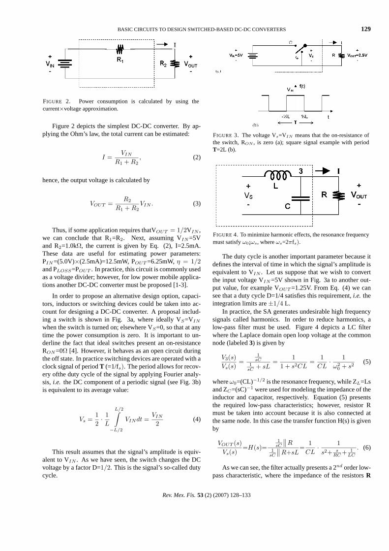
In order to propose an alternative design option, capaci-tors, inductors or switching devices could be taken into ac-count for designing a DC-DC converter. A proposal includ-ing a switch is shown in Fig. 3a, where ideally VS=VIN
when the switch is turned on; elsewhere VS=0, so that at anytime the power consumption is zero. It is important to un-derline the fact that ideal switches present an on-resistanceRON=0Ω [4]. However, it behaves as an open circuit duringthe off state. In practice switching devices are operated with aclock signal of periodT (=1/fs). The period allows for recov-ery ofthe duty cycle of the signal by applying Fourier analy-sis, i.e. the DC component of a periodic signal (see Fig. 3b)is equivalent to its average value:
Vs =12· 1L
L/2∫
−L/2
VINdt =VIN
2(4)
This result assumes that the signal’s amplitude is equiv-alent to VIN . As we have seen, the switch changes the DCvoltage by a factor D=1/2. This is the signal’s so-called dutycycle.
FIGURE 3. The voltage Vs=VIN means that the on-resistance ofthe switch, RON , is zero (a); square signal example with periodT=2L (b).
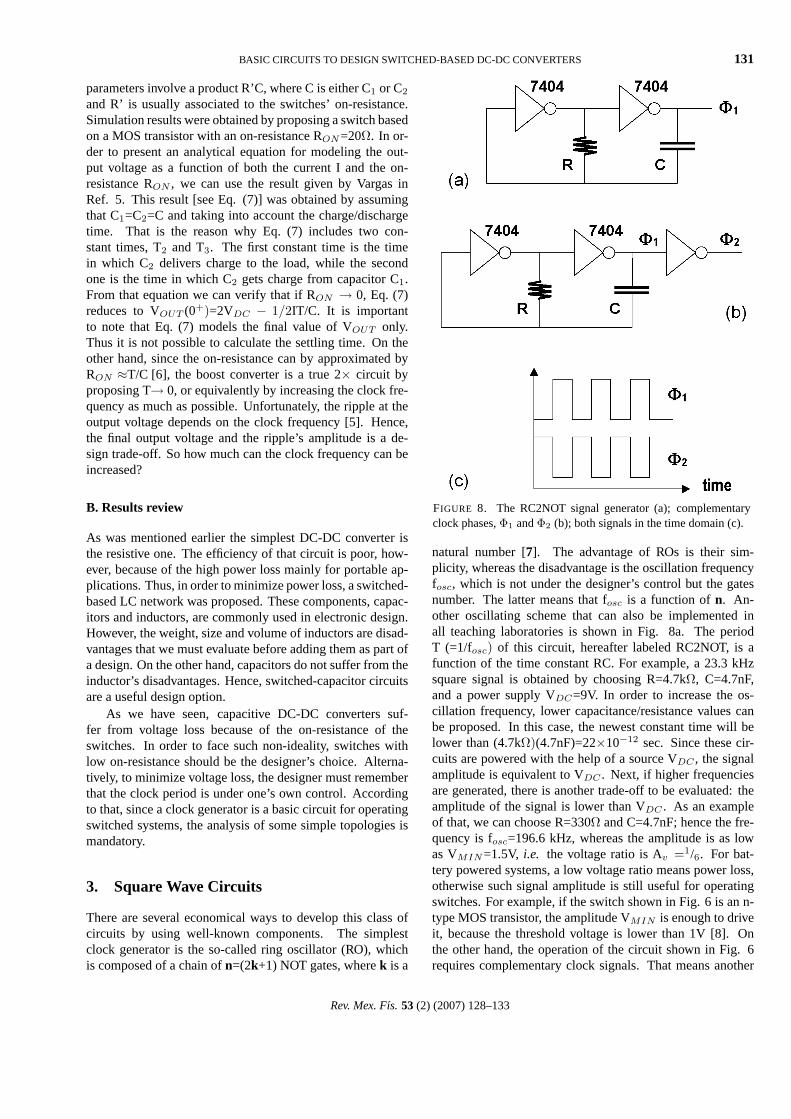
FIGURE 4. To minimize harmonic effects, the resonance frequencymust satisfyω0¡ωs, whereωs=2πfs).
The duty cycle is another important parameter because itdefines the interval of time in which the signal’s amplitude isequivalent to VIN . Let us suppose that we wish to convertthe input voltage VIN=5V shown in Fig. 3a to another out-put value, for example VOUT =1.25V. From Eq. (4) we cansee that a duty cycle D=1/4 satisfies this requirement,i.e. theintegration limits are±1/4 L.
In practice, the SA generates undesirable high frequencysignals called harmonics. In order to reduce harmonics, alow-pass filter must be used. Figure 4 depicts a LC filterwhere the Laplace domain open loop voltage at the commonnode (labeled3) is given by
V3(s)Vs(s)
=1
sC1
sC + sL=
11 + s2CL
=1
CL· 1ω2
0 + s2(5)
whereω0=(CL)−1/2 is the resonance frequency, while ZL=Lsand ZC=(sC)−1 were used for modeling the impedance of theinductor and capacitor, respectively. Equation (5) presentsthe required low-pass characteristics; however, resistor Rmust be taken into account because it is also connected atthe same node. In this case the transfer function H(s) is givenby
VOUT (s)Vs(s)
=H(s)=1
sC
∥∥R1
sC
∥∥ R+sL=
1CL
· 1s2+ s
RC + 1LC
. (6)
As we can see, the filter actually presents a 2nd order low-pass characteristic, where the impedance of the resistorsR
Rev. Mex. Fıs. 53 (2) (2007) 128–133

130 F. SANDOVAL-IBARRA, J.R. MERCADO-MORENO, AND L.H. URIOSTEGUI-VAZQUEZ
affects the filter’s quality factor only. This sounds good, be-cause the resonance frequency is just a function of the LCnetwork as was found before.
Since passive components and switches are non-ideal net-work components, the efficiency is lower than 100%. As weshall see, switching frequencyωs plays a basic role not onlyin the dynamic power consumption but also for calculatingthe passive component values.
A. Boost Converter
This converter includes an inductor L between the DC volt-age source and the switching devic, as Fig. 5 shows. At thispoint we can see, on one hand, how many components aresubstituting for the resistor R1 shown in Fig. 2 and, on theother hand, we can not forget that the main objective is tominimize power loss. The advantage of the boost converteris that voltages higher than VIN can be obtained, whereas thedisadvantage is related to inductors because of their weight,size and volume.
The LC-based boost converter is not the only proposalfor reducing power loss. Figure 6a shows a purely capaci-tive boost converter, which works with complementary clocksignals, Φ1 and Φ2. In order to analyze how this con-verter works, we shall assume that an open switch models anopen circuit(ROFF → ∞), otherwise the switch is closed,RON=0Ω. Then, ifΦ1=“1” (Φ2=“0”), the equivalent circuitis shown in Fig. 6b. We can see that the voltage drop in C1
is equal to VDC while C2 keeps its original charge. Next,Φ2=“1” (Φ1=“0”) and the output voltage is VDC plus thevoltage drop in C1 (see Fig. 6c). In other words, the outputvoltage is equivalent to the series connection of two voltagesources. Consequently, this circuit is ideally a voltage multi-plier or a 2× circuit. Figure 7 shows simulation results of thiscircuit, where VDC=1.5V was proposed. From these resultssome conclusions are obtained:
• there is a settling time St = 250µs.
• the output voltage is of the order of 2.8V, and
• the voltage ratio is Av=VOUT /VDC=1.86.
So why is the capacitive DC-DC converter not a 2× cir-cuit? In the ideal analysis, neither current I nor RON (> 0Ω)were taken into account. In other words, voltage loss a isfunction of the charge and discharge time of capacitors. Both
FIGURE 5. The boost converter. In practice the switch is a semi-conductor device.
FIGURE 6. Capacitive boost converter (a); equivalent circuit atΦ1=”1” (b); during the timeΦ2=”1” an ideal 2× circuit is ob-tained (c).
FIGURE 7. Simulation result of the 2× circuit with VDC=1.5V,RON =20Ω, C=0.1µF and I=1mA.
Rev. Mex. Fıs. 53 (2) (2007) 128–133
BASIC CIRCUITS TO DESIGN SWITCHED-BASED DC-DC CONVERTERS 131
parameters involve a product R’C, where C is either C1 or C2
and R’ is usually associated to the switches’ on-resistance.Simulation results were obtained by proposing a switch basedon a MOS transistor with an on-resistance RON=20Ω. In or-der to present an analytical equation for modeling the out-put voltage as a function of both the current I and the on-resistance RON , we can use the result given by Vargas inRef. 5. This result [see Eq. (7)] was obtained by assumingthat C1=C2=C and taking into account the charge/dischargetime. That is the reason why Eq. (7) includes two con-stant times, T2 and T3. The first constant time is the timein which C2 delivers charge to the load, while the secondone is the time in which C2 gets charge from capacitor C1.From that equation we can verify that if RON → 0, Eq. (7)reduces to VOUT (0+)=2VDC − 1/2IT/C. It is importantto note that Eq. (7) models the final value of VOUT only.Thus it is not possible to calculate the settling time. On theother hand, since the on-resistance can by approximated byRON ≈T/C [6], the boost converter is a true 2× circuit byproposing T→ 0, or equivalently by increasing the clock fre-quency as much as possible. Unfortunately, the ripple at theoutput voltage depends on the clock frequency [5]. Hence,the final output voltage and the ripple’s amplitude is a de-sign trade-off. So how much can the clock frequency can beincreased?
B. Results review
As was mentioned earlier the simplest DC-DC converter isthe resistive one. The efficiency of that circuit is poor, how-ever, because of the high power loss mainly for portable ap-plications. Thus, in order to minimize power loss, a switched-based LC network was proposed. These components, capac-itors and inductors, are commonly used in electronic design.However, the weight, size and volume of inductors are disad-vantages that we must evaluate before adding them as part ofa design. On the other hand, capacitors do not suffer from theinductor’s disadvantages. Hence, switched-capacitor circuitsare a useful design option.
As we have seen, capacitive DC-DC converters suf-fer from voltage loss because of the on-resistance of theswitches. In order to face such non-ideality, switches withlow on-resistance should be the designer’s choice. Alterna-tively, to minimize voltage loss, the designer must rememberthat the clock period is under one’s own control. Accordingto that, since a clock generator is a basic circuit for operatingswitched systems, the analysis of some simple topologies ismandatory.
3. Square Wave Circuits
There are several economical ways to develop this class ofcircuits by using well-known components. The simplestclock generator is the so-called ring oscillator (RO), whichis composed of a chain ofn=(2k+1) NOT gates, wherek is a
FIGURE 8. The RC2NOT signal generator (a); complementaryclock phases,Φ1 andΦ2 (b); both signals in the time domain (c).
natural number [7]. The advantage of ROs is their sim-plicity, whereas the disadvantage is the oscillation frequencyfosc, which is not under the designer’s control but the gatesnumber. The latter means that fosc is a function ofn. An-other oscillating scheme that can also be implemented inall teaching laboratories is shown in Fig. 8a. The periodT (=1/fosc) of this circuit, hereafter labeled RC2NOT, is afunction of the time constant RC. For example, a 23.3 kHzsquare signal is obtained by choosing R=4.7kΩ, C=4.7nF,and a power supply VDC=9V. In order to increase the os-cillation frequency, lower capacitance/resistance values canbe proposed. In this case, the newest constant time will belower than (4.7kΩ)(4.7nF)=22×10−12 sec. Since these cir-cuits are powered with the help of a source VDC , the signalamplitude is equivalent to VDC . Next, if higher frequenciesare generated, there is another trade-off to be evaluated: theamplitude of the signal is lower than VDC . As an exampleof that, we can choose R=330Ω and C=4.7nF; hence the fre-quency is fosc=196.6 kHz, whereas the amplitude is as lowas VMIN=1.5V, i.e. the voltage ratio is Av =1/6. For bat-tery powered systems, a low voltage ratio means power loss,otherwise such signal amplitude is still useful for operatingswitches. For example, if the switch shown in Fig. 6 is an n-type MOS transistor, the amplitude VMIN is enough to driveit, because the threshold voltage is lower than 1V [8]. Onthe other hand, the operation of the circuit shown in Fig. 6requires complementary clock signals. That means another
Rev. Mex. Fıs. 53 (2) (2007) 128–133

132 F. SANDOVAL-IBARRA, J.R. MERCADO-MORENO, AND L.H. URIOSTEGUI-VAZQUEZ
NOT gate must be added to satisfy that requirement. Thenewest circuit is depicted in Fig. 8b, while Fig. 8c showsboth signals. The latter follows an illustrative purpose, andno DC level are assumed.
VOUT = 2VDC − I
2C
[T + T2
(1− e−T2/RON C
)]
×(
32
+ e−T/4RON C
)− I
[T3
C
(1 + e−T/4RON C
)
−2RON
(3 + e−T3/RON C
) T3
T
](7)
Circuits using complementary signals suffer power lossif some cautions are omitted. For example, when signalΦ1
goes from1 to 0, Φ2 operates from0 to 1; that means thereis a time∆t in which both switches are turned on,i.e. theswitch’s on-resistance consumes power. To achieve powersavings that minimize power losses, a non-overlap signalsgenerator must be designed. One proposal is shown in Fig. 9,where the input signal could be the response given by theRC2NOT oscillator. Here, the output NOT gates introduce anon-overlap region because of the gates’ delay.
Figure 10 shows experimental results of the circuit shownin Fig. 9, where the response was captured by using aTDS2014 Tektronix Digital Oscilloscope. From this figurenothing can be said about the non-overlap region; however,by doing a close-up (see Fig. 11), such, region can be iden-tified. In practice, a non-overlap region can be obtained byknowing the importance of the gate’s logic threshold voltage,VLTH . That parameter, associated with a NOT gate, is ap-proximately1/2VDC because of symmetry considerations.In fact, at the input voltage equal to1/2VDC , the NOT gatedrives its maximum current. This is the reason why reducingVLTH save power is done.
Figure 11a shows the logical transition of both sig-nals (Φ1: 1→0, Φ2: 0→1), where it is easy to see thatVTHL < 1/2VDC . This performance indicates that oneswitch is first turned off and then the second switch is turnedon. The same is true for the next logic transitions shown inFig. 11b (Φ1: 0→1, Φ2: 1→0), where VLTH is lower than1/2VDC . Hence, a non-overlap signal generator certainlysaves power.
FIGURE 9. Basic circuit for generating a non-overlap region be-tween clock signals.
FIGURE 10. Experimental response of the circuit shown in Fig. 10,where fosc=35.7 kHz and VDC=10V.
FIGURE 11. The non-overlap regions between signals. HereR=330Ω and C=22nF were used.
A. Laboratory
As we have seen, the frequency of the RC2NOT oscilla-tor was as high as 196.6 kHz for a power supply VDC=9V.An additional activity for the reader is the circuit shown inFig. 12, where NAND gates are used. This circuit, labeledhereafter RC2NAND, generates a clock signal up to 1.6 MHzfor a power supply VDC=9V. Also, the reader must test thedesign of a ring oscillator by varying the number of NOTgates. In this case, experimental data will indicate the fre-quency value as a function ofn. In fact, different frequencyvalues are obtained by proposing other VDC values.
Rev. Mex. Fıs. 53 (2) (2007) 128–133
BASIC CIRCUITS TO DESIGN SWITCHED-BASED DC-DC CONVERTERS 133
FIGURE 12. The RC2NAND oscillator circuit.
4. Conclusions
As we have seen, circuits based on the switched approach usea clock generator. Throughout this paper, non-idealities asso-ciated with DC-DC converters were discussed in order to un-derline advantages/disadvantages between different DC-DCtopologies. Disadvantages, on one hand, are related to bothvoltage and power loss because of resistive components. Onthe other hand, in order to save power, resistors have beensubstituted by alternative components, switches and capac-itors being the best choice. However, switches present in-trinsic resistance that also represents power losses; thus, inlooking for solutions to face such non-ideality, increasing theclock frequency fosc was a proposed design option.
Low-cost components, including batteries, were used toimplement simple clock generators. These circuits are non-
complex and can be implemented in any electronics labora-tory. Since physical implementation allows the trainees toverify design specifications and also take into account designconstrain, it is possible introduce uncommon topics in aca-demic curricula in order to introduce analysis, design and op-timization techniques. According to this, authors in this pa-per have used a DC-DC converter as a vehicle for presentingbasics on switched techniques and mentioning some powerelectronics definitions.
A whole design is not a individual work but team work.However, throughout this paper non-idealities were under-lined in order to analyze the efficiency of the converter as wellas to eliminate components that induce power loss. Once theimportance of the clock frequency in the design of high per-formance circuits has been analyzed, future work includes ananalysis about how to select switching devices and why sucha choice introduces additional non-idealities effects.
Finally, readers should implement clock generators pre-sented here and propose other circuits by taking into accountthe fact that a clock generator works under a couple of re-quirements: feedback positively an inverting gain stage. Ac-cording to this, simple analog circuits can also be used fordesigning oscillator circuits.
Acknowledgments
Authors wish to thank the anonymous reviewer for his helpfulcomments and critical review.
1. F. Callias, F.H. Salchli, and D. Girard,IEEE Journal of Solid-State Circuits24 (1989).
2. L.S.Y. Wonget al., IEEE J. of Solid-State Circuits39 (2004)2446.
3. K. Lee, S.J. Lee, and H.J. Yoo,IEEE Trans. on VLSI Sys.14(2006) 148.
4. V. Litivsky, M. Saviæ, andZ. Mræarica,HAIT J. of Sc. and Eng.B. 2 (2005) 476.
5. E. Vargas-Calderon and M.S. thesis, CINVESTAV-GuadalajaraUnit, Jalisco, Mexico, 2005 (in Spanish).
6. J. Terryet al, IEEE J. of Solid-State CircuitsSC-12(1977) 592.
7. F. Sandoval-Ibarra and E. Montoya-Suarez,Rev. Mex. Fıs. E50(2004) 114.
8. R.S. Muller and T.I. Kamins,Electronica de los Disposi-tivos para Circuitos Integrados, 1st edition (LIMUSA, Mexico,1982) p. 454.
Rev. Mex. Fıs. 53 (2) (2007) 128–133