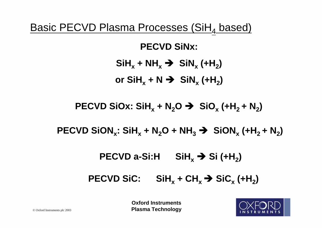
basic pecvd plasma processes (sih based)
TRANSCRIPT
Oxford Instruments Plasma Technology© Oxford Instruments plc 2003
Basic PECVD Plasma Processes (SiH4 based)
PECVD SiNx:
SiHx + NHx SiNx (+H2)
or SiHx + N SiNx (+H2)
PECVD SiOx: SiHx + N2O SiOx (+H2 + N2)
PECVD a-Si:H SiHx Si (+H2)
PECVD SiC: SiHx + CHx SiCx (+H2)
PECVD SiONx: SiHx + N2O + NH3 SiONx (+H2 + N2)

Oxford Instruments Plasma Technology© Oxford Instruments plc 2003
Types of SiH4 supply
SiH4 can be supplied as either pure SiH4 or dilute in an ‘inert’ carrier gas , typically N2, Ar, He.
Typical percentage dilutions are 5%, or 2% or 10%.
When converting a recipe for a different SiH4 dilutions, always remember that it is the SiH4 flow that is important:
400sccm 5%SiH4/N2 = 20sccm SiH4 + 380 sccm N2
So you will need to flow 1000sccm 2%SiH4/N2 to achieve the same SiH4 flow.
The effect of the additional N2 flow will be minimal, and can sometimes be compensated for by reducing the separate N2 MFC flow (if applicable).
Important note: Always remember to check rotary pump purge is suitable for maximum SiH4 flow:
Purge flow (litres/min) > 3 x max SiH4 flow (sccm) / 14
Oxford Instruments Plasma Technology© Oxford Instruments plc 2003
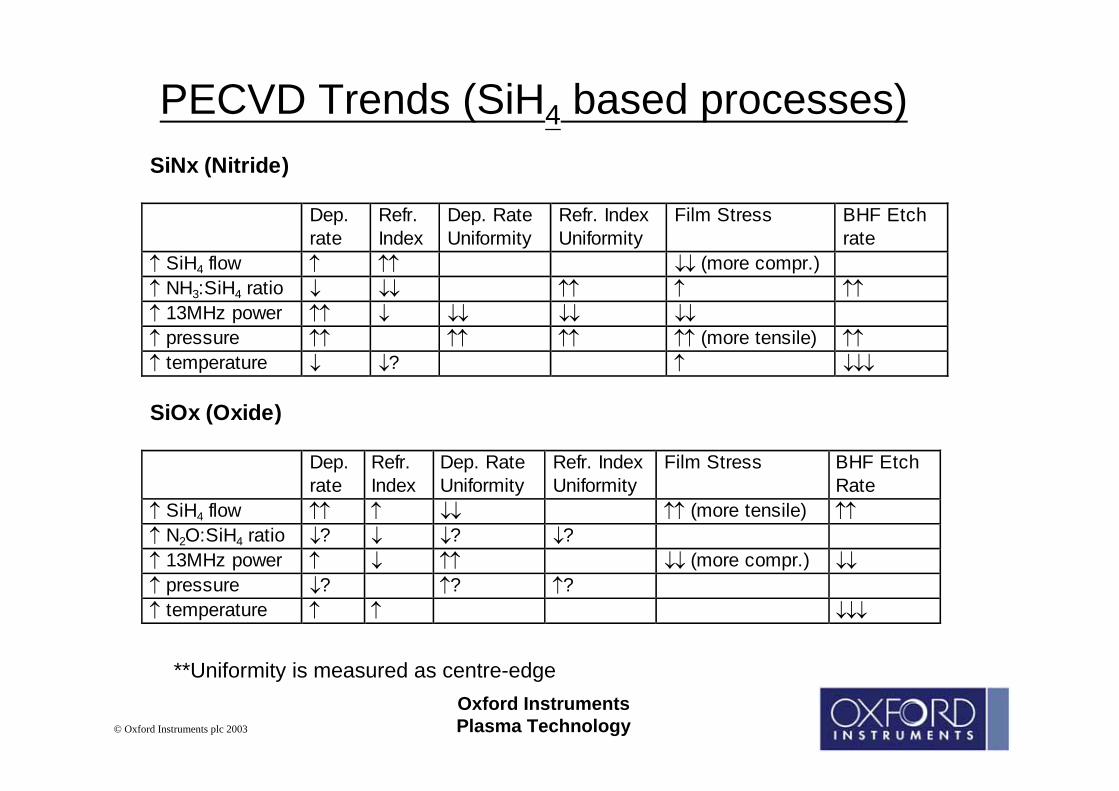
PECVD Trends (SiH4 based processes)SiNx (Nitride) Dep.
rate Refr. Index
Dep. Rate Uniformity
Refr. Index Uniformity
Film Stress BHF Etch rate
↑ SiH4 flow ↑ ↑↑ ↓↓ (more compr.) ↑ NH3:SiH4 ratio ↓ ↓↓ ↑↑ ↑ ↑↑ ↑ 13MHz power ↑↑ ↓ ↓↓ ↓↓ ↓↓ ↑ pressure ↑↑ ↑↑ ↑↑ ↑↑ (more tensile) ↑↑ ↑ temperature ↓ ↓? ↑ ↓↓↓ SiOx (Oxide) Dep.
rate Refr. Index
Dep. Rate Uniformity
Refr. Index Uniformity
Film Stress BHF Etch Rate
↑ SiH4 flow ↑↑ ↑ ↓↓ ↑↑ (more tensile) ↑↑ ↑ N2O:SiH4 ratio ↓? ↓ ↓? ↓? ↑ 13MHz power ↑ ↓ ↑↑ ↓↓ (more compr.) ↓↓ ↑ pressure ↓? ↑? ↑? ↑ temperature ↑ ↑ ↓↓↓
**Uniformity is measured as centre-edge
Oxford Instruments Plasma Technology© Oxford Instruments plc 2003
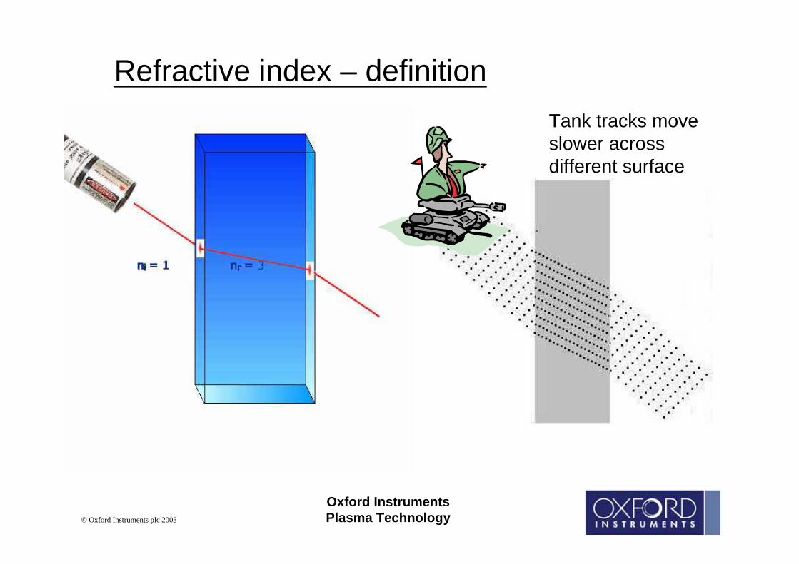
Refractive index – definitionTank tracks move slower across different surface

Oxford Instruments Plasma Technology© Oxford Instruments plc 2003
Refractive index – why is it important in PECVD?
Refractive index is a good indicator of film composition, i.e. Si:Nratio or Si:O ratio.
(If Si content is high, the refractive index will be high)
It can be easily measured by ellipsometer or prism coupler, allowing rapid evaluation of film composition (and unifomrity of composition).
Oxford Instruments Plasma Technology© Oxford Instruments plc 2003
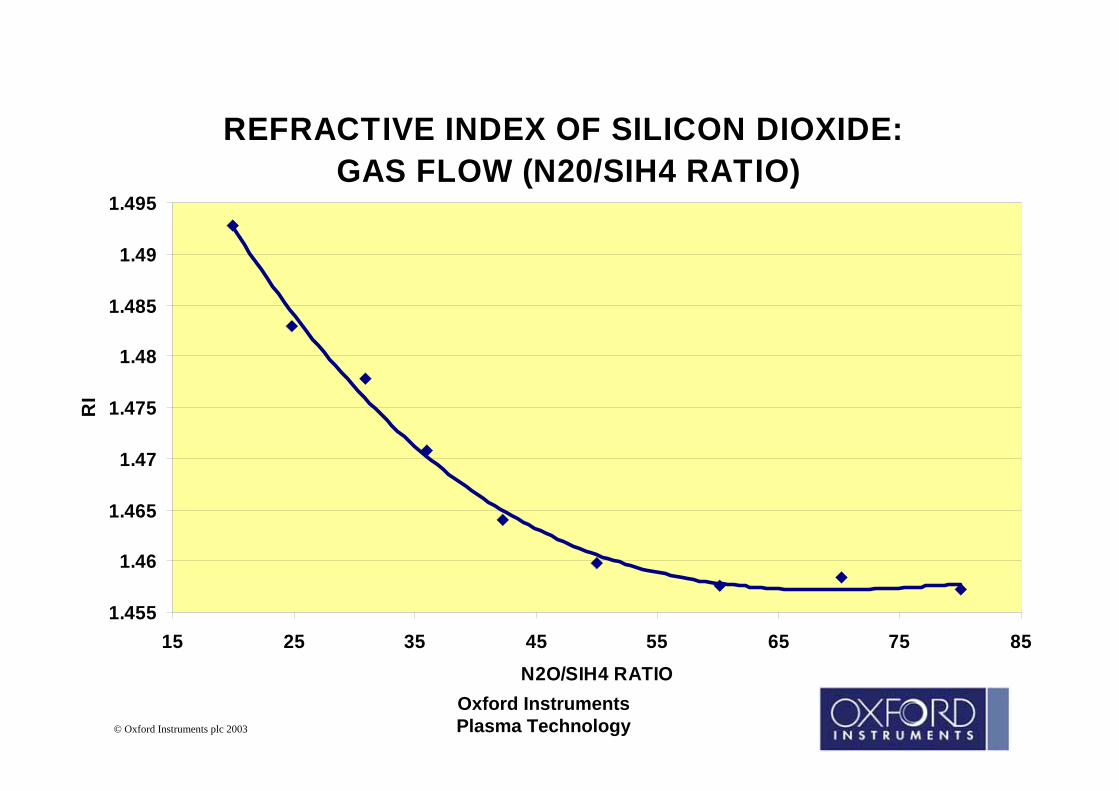
REFRACTIVE INDEX OF SILICON DIOXIDE: GAS FLOW (N20/SIH4 RATIO)
1.455
1.46
1.465
1.47
1.475
1.48
1.485
1.49
1.495
15 25 35 45 55 65 75 85N2O/SIH4 RATIO
RI
Oxford Instruments Plasma Technology© Oxford Instruments plc 2003
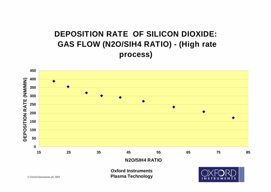
DEPOSITION RATE OF SILICON DIOXIDE:GAS FLOW (N2O/SIH4 RATIO) - (High rate
process)
0
50
100
150
200
250
300
350
400
450
15 25 35 45 55 65 75 85
N2O/SIH4 RATIO
DEP
OSI
TIO
N R
ATE
(NM
/MIN
)

Oxford Instruments Plasma Technology© Oxford Instruments plc 2003
SiONx refractive index controlRefractive index vs N2O : SiH4 : ratio
1.45
1.46
1.47
1.48
1.49
1.5
1.51
30 40 50 60 70
N2O : SiH4
RI
With 100 sccm NH3
Without NH3
Refractive index vs NH3 flow
1.4581.46
1.4621.4641.4661.468
1.471.4721.474
0 20 40 60 80 100 120
NH3 flow (sccm )R
I
Oxford Instruments Plasma Technology© Oxford Instruments plc 2003
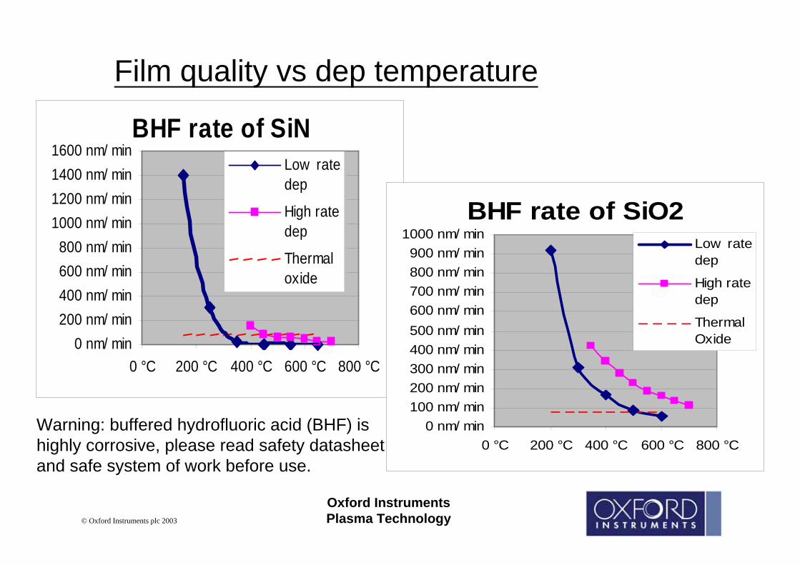
Film quality vs dep temperature
Warning: buffered hydrofluoric acid (BHF) is highly corrosive, please read safety datasheet and safe system of work before use.
BHF rate of SiN
0 nm/ min200 nm/ min400 nm/ min600 nm/ min800 nm/ min
1000 nm/ min1200 nm/ min1400 nm/ min1600 nm/ min
0 °C 200 °C 400 °C 600 °C 800 °C
Low ratedep
High ratedep
Thermaloxide
BHF rate of SiO2
0 nm/ min100 nm/ min200 nm/ min300 nm/ min400 nm/ min500 nm/ min600 nm/ min700 nm/ min800 nm/ min900 nm/ min
1000 nm/ min
0 °C 200 °C 400 °C 600 °C 800 °C
Low ratedep
High ratedep
ThermalOxide
Oxford Instruments Plasma Technology© Oxford Instruments plc 2003
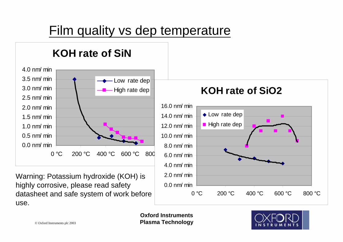
Film quality vs dep temperature
Warning: Potassium hydroxide (KOH) is highly corrosive, please read safety datasheet and safe system of work before use.
KOH rate of SiN
0.0 nm/ min0.5 nm/ min1.0 nm/ min1.5 nm/ min2.0 nm/ min2.5 nm/ min3.0 nm/ min3.5 nm/ min4.0 nm/ min
0 °C 200 °C 400 °C 600 °C 800 °C
Low rate depHigh rate dep KOH rate of SiO2
0.0 nm/ min
2.0 nm/ min
4.0 nm/ min
6.0 nm/ min8.0 nm/ min
10.0 nm/ min
12.0 nm/ min
14.0 nm/ min
16.0 nm/ min
0 °C 200 °C 400 °C 600 °C 800 °C
Low rate dep
High rate dep
Oxford Instruments Plasma Technology© Oxford Instruments plc 2003
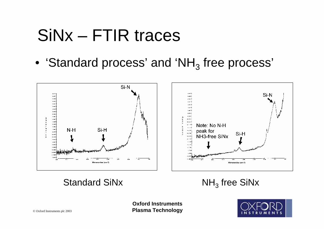
SiNx – FTIR traces• ‘Standard process’ and ‘NH3 free process’
Standard SiNx NH3 free SiNx
Oxford Instruments Plasma Technology© Oxford Instruments plc 2003
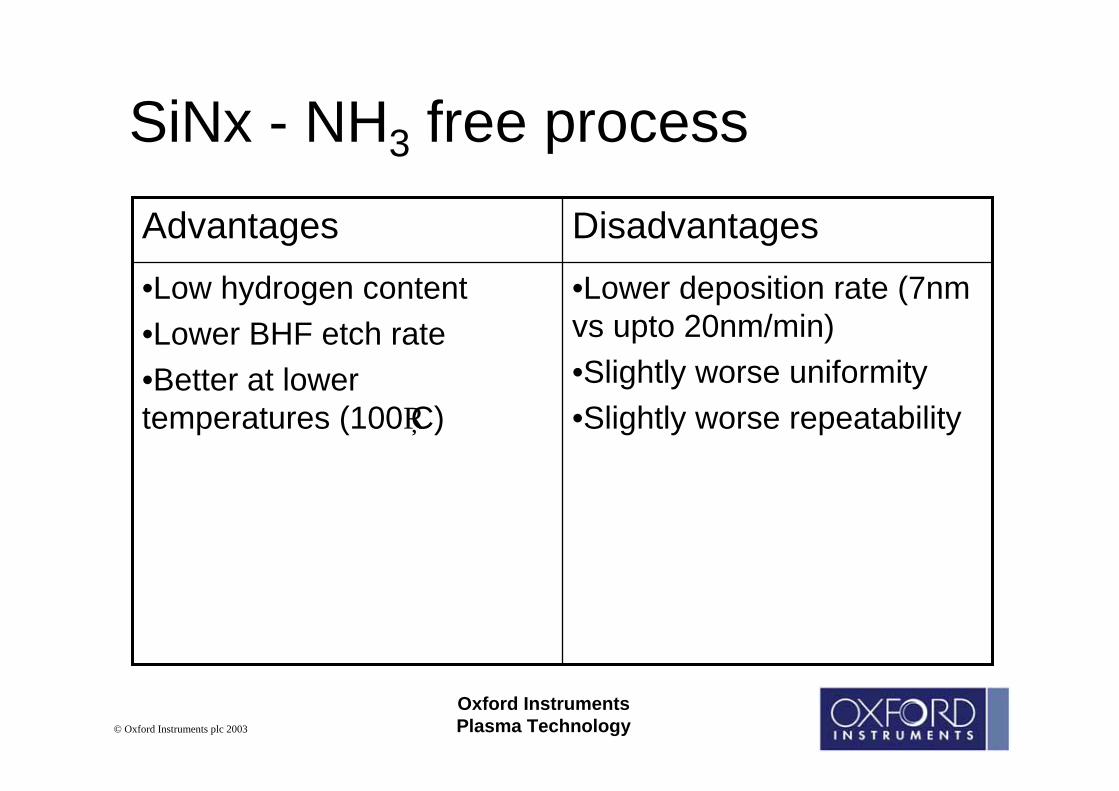
SiNx - NH3 free process
•Lower deposition rate (7nm vs upto 20nm/min)•Slightly worse uniformity•Slightly worse repeatability
•Low hydrogen content•Lower BHF etch rate•Better at lower temperatures (100°C)
DisadvantagesAdvantages
Oxford Instruments Plasma Technology© Oxford Instruments plc 2003
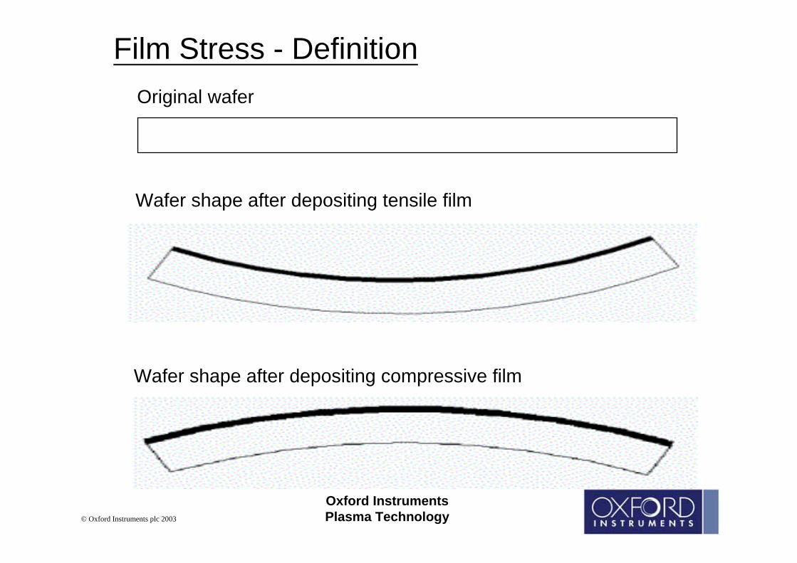
Film Stress - DefinitionOriginal wafer
Wafer shape after depositing tensile film
Wafer shape after depositing compressive film

Oxford Instruments Plasma Technology© Oxford Instruments plc 2003
Film Stress - DefinitionThe causes of film stress can be visualised by imagining what happens when too many atoms are packed into the film - bond lengths are pushed shorter than normal – the film tries to relax back to its normal bond length – pushing outwards and forcing a convex ‘compressive stress’ curvature of the wafer.
The opposite happens for tensile stress – too few atoms per cm3 – tensile films are usually less dense than compressive films.
The convention is: negative sign for compressive stress, positive sign for tensile.

Oxford Instruments Plasma Technology© Oxford Instruments plc 2003
Film Stress - Definition
ratioPoisson modulus, Youngs
thicknessfilm and substrate and
scan of radius bow,in wafer change
stress film :where
2
2 )1(3.)(.
==
=
==∆
=
−∆
=
υE
filmtsubstratet
r
film
substrate Et
tr
σ
υσ
∆, r, and thicknesses must be measured in the same unit, e.g. cm or µm
Then σ will be in the same units as E (e.g. dynes/cm2 or GPa)

Oxford Instruments Plasma Technology© Oxford Instruments plc 2003
Film Stress - Definitionfor silicon:
cmdynes x . xfilm
substrate
tt
r211
10166 2
2
)(.∆=σ
cmdynes x . x 21110166
5.0)500(.
)25000(10 2
2=σ
Example: 10µm bow on 25mm radius scan, 500µm Si substrate, 0.5µm film:
(OR 61.6 GPa OR 61600 MPa)
493MPa 0.493GPa 29104.93 === cmdynes x σ

Oxford Instruments Plasma Technology© Oxford Instruments plc 2003
At 13.56MHz, ions do not respond to RF field
At 100-350kHz, ions can respond and give
ion bombardment of growing film
Mixing of High and Low frequency power allows control over ion bombardment and hence control
over film stress and film density
Mixed frequency PECVD
Oxford Instruments Plasma Technology© Oxford Instruments plc 2003
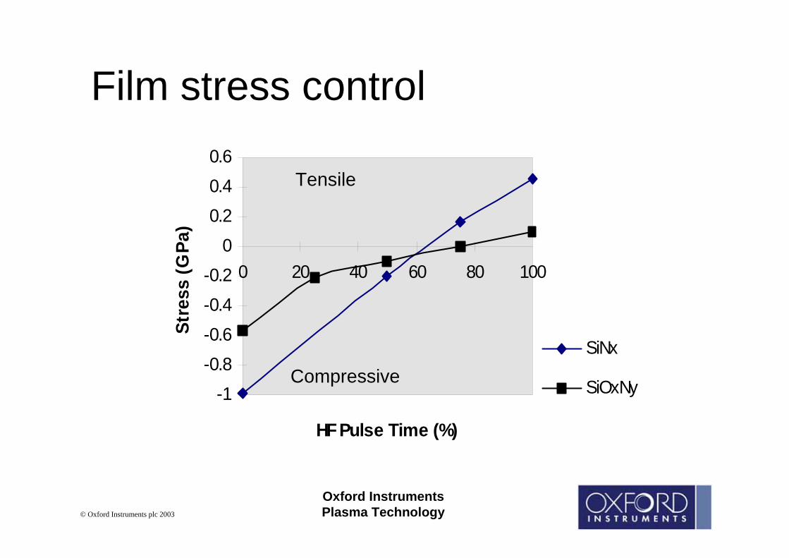
-1-0.8-0.6-0.4-0.2
00.20.40.6
0 20 40 60 80 100
HF Pulse Time (%)
Stre
ss (G
Pa)
SiNx
SiOxNy
Tensile
Compressive
Film stress control
Oxford Instruments Plasma Technology© Oxford Instruments plc 2003
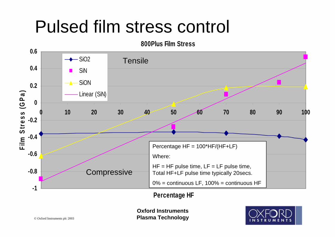
800Plus Film Stress
-1
-0.8
-0.6
-0.4
-0.2
0
0.2
0.4
0.6
0 10 20 30 40 50 60 70 80 90 100
Percentage HF
Film
Str
ess
(GPa
)
SiO2
SiN
SiON
Linear (SiN)
Percentage HF = 100*HF/(HF+LF)
Where:
HF = HF pulse time, LF = LF pulse time, Total HF+LF pulse time typically 20secs.
0% = continuous LF, 100% = continuous HF
Tensile
Compressive
Pulsed film stress control

Oxford Instruments Plasma Technology© Oxford Instruments plc 2003
REFRACTIVE INDEX OF SILICON DIOXIDE: GAS FLOW (N20/SIH4 RATIO)
1.455
1.46
1.465
1.47
1.475
1.48
1.485
1.49
1.495
15 25 35 45 55 65 75 85N2O/SIH4 RATIO
RI
Stress control SiOx• Reduce RF power• Adjustment of N2O:SiH4 ratio
-300MPa (low rate)
-100MPa (high rate)
0 - -50MPa
Oxford Instruments Plasma Technology© Oxford Instruments plc 2003
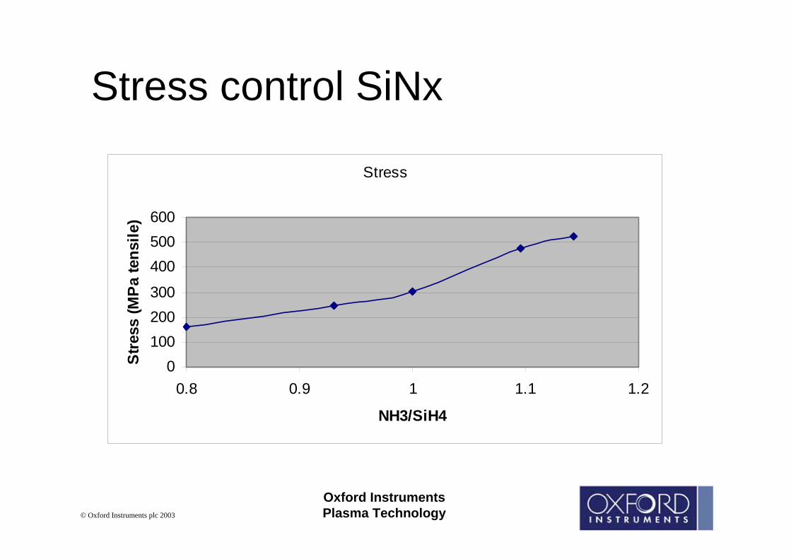
Stress control SiNx
Stress
0100200300
400500600
0.8 0.9 1 1.1 1.2
NH3/SiH4
Stre
ss (M
Pa
tens
ile)
Oxford Instruments Plasma Technology© Oxford Instruments plc 2003
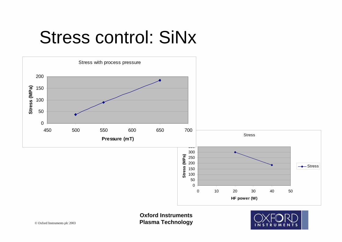
Stress control: SiNx
Stress
050
100150200250300350
0 10 20 30 40 50
HF power (W)
Stre
ss (M
Pa)
Stress
Stress with process pressure
0
50
100
150
200
450 500 550 600 650 700
Pressure (mT)
Stre
ss (M
Pa)
Oxford Instruments Plasma Technology© Oxford Instruments plc 2003
a-Si:H
• Deposited using SiH4
• Either pure, He or Ar dilution• Common for addition of PH3 and B2H6 as dopant• Surface pre-cleans useful for surface adhesion
improvements• Bubbling of film may result when depositing on to bare Si
wafers• Usually deposited on to SiOx or SiNx underlayer• Stress dependant on underlayer

Oxford Instruments Plasma Technology© Oxford Instruments plc 2003
a-Si: stress control: SiOx underlying film
Stress vs SiH4 flow
-250
-200
-150
-100
-50
015 16 17 18 19 20
SiH4 flow
Stre
ss (M
Pa)
Stress
Oxford Instruments Plasma Technology© Oxford Instruments plc 2003
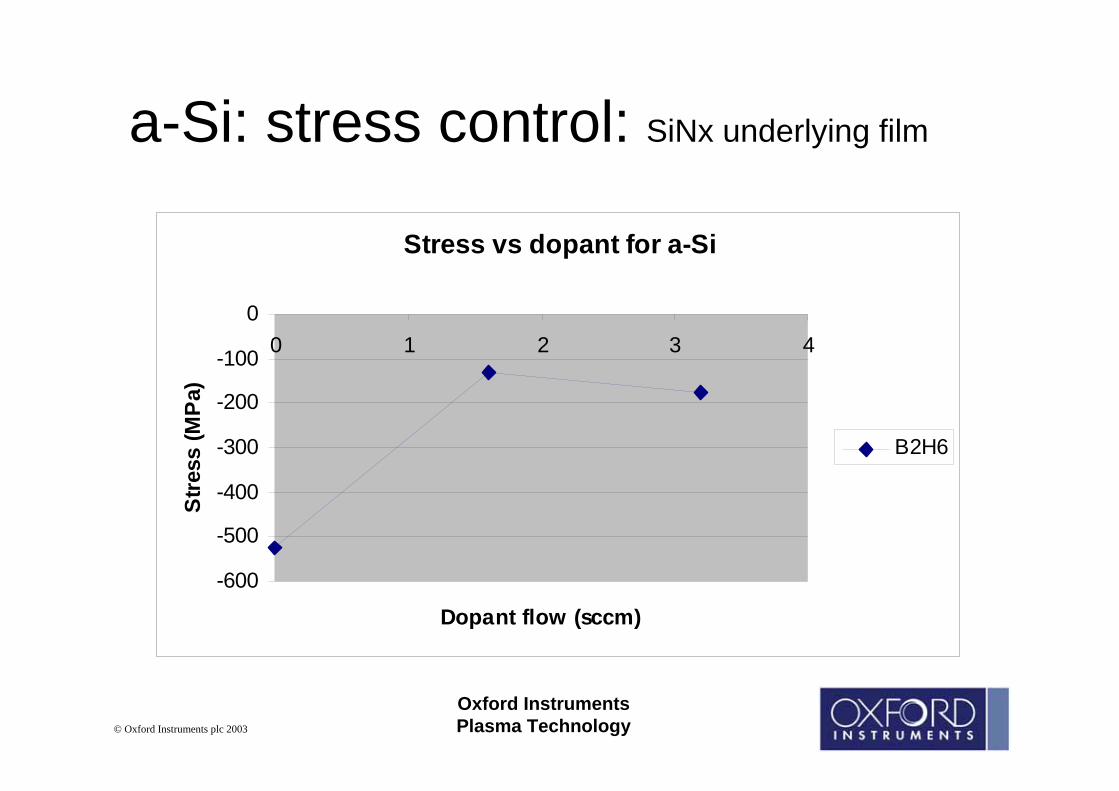
a-Si: stress control: SiNx underlying film
Stress vs dopant for a-Si
-600
-500
-400
-300
-200
-100
00 1 2 3 4
Dopant flow (sccm)
Stre
ss (M
Pa)
B2H6
Oxford Instruments Plasma Technology© Oxford Instruments plc 2003
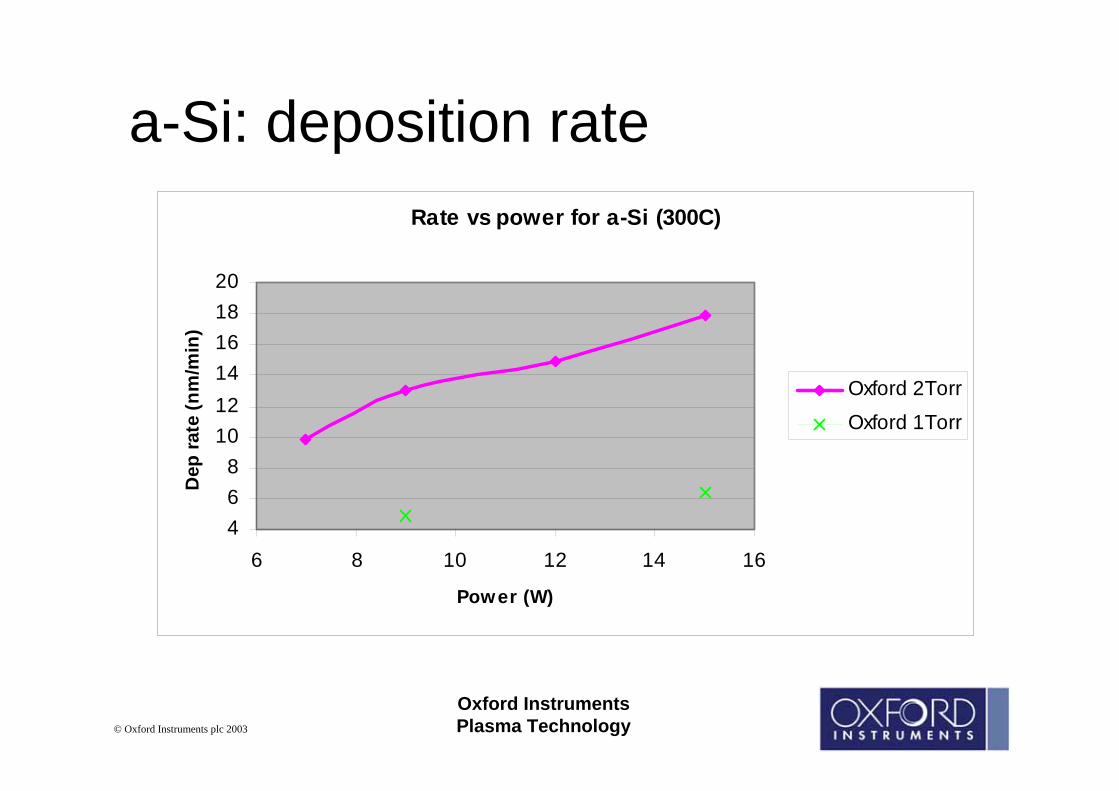
a-Si: deposition rateRate vs power for a-Si (300C)
468
101214161820
6 8 10 12 14 16
Power (W)
Dep
rate
(nm
/min
)
Oxford 2Torr
Oxford 1Torr
Oxford Instruments Plasma Technology© Oxford Instruments plc 2003
• Poor adhesion – change chemistry of, or lengthen, surface preclean step
• Surface interactions – deposit SiNx at <300C on InP to avoid rough/lumpy films - or use NH3-free SiNx
• Particles – if seen as silica dust in showerhead pattern on wafers then need to search for air leaks in gas lines or behind showerhead. Or increase pump/purge cycle after chamber cleaning.
• Particles - if random scattering of particles check chamber/showerhead condition – may need plasma cleaning or sandblasting clean.
• Pinholes – as for particles above.
Common PECVD problems

Oxford Instruments Plasma Technology© Oxford Instruments plc 2003
Particle descriptions When they most often occur
Possible causes Remedy/Quick Fix –Test
Small particles less than 5um which appear in concentrated clusters. These clusters appear in a pattern which mirrors that of the showerhead holes.
They are concentrated mainly in one focal plane of the microscope and appear to be at the bottom of the film.
The first run after a clean Running the machine too soon after the completion of a clean process. Silane forms particles when it reacts with residual oxygen in the gas lines (remember all of the gas line up to the normally open, hardware interlock nupro valve is incorporated in the chamber vacuum and needs to de-gas at the end of a long clean run).
Wait 30 minutes before running a deposition process using silaneafter finishing a clean.
Small particles less than 5um which appear in concentrated clusters. These clusters appear in a pattern which mirrors that of the showerhead holes.
They are concentrated mainly in one focal plane of the microscope and appear to be at the bottom of the film.
The first run after a long period of machine disuse (say overnight)
A small leak in the silane line, particularly around the mass flow, allowing a build-up of silane dust which is blown though on to the first wafer.
Fix the leak in the silane line. Flow silane gas after a significant period of machine disuse without a wafer in the chamber to clear the dust.
Small particles less than 5um which appear in concentrated clusters. These clusters appear in a pattern which may or may not mirror that of the showerhead holes.
They appear in many different focal planes of the microscope, at regular intervals throughout the film.
Every run A leak in the gas in-let assembly or a severe leak in the silane line.
Plasma forming behind the showerhead or in the gas inlet assembly.
Leak check chamber and gas line. If both less than 1mT per minute contact Oxford service department and give this description. If greater than 1 mTper minute take apart gas inlet assembly and clean O-rings and PTFE part.

Oxford Instruments Plasma Technology© Oxford Instruments plc 2003
Flakes or larger non-metallic particles
First run after a clean Residual particles not etched during the cleaning process
Vacuum the chamber inside, this is necessary periodically after cleaning. It may be a good idea to cool the chamber first to prevent risk of injury with the hot table.
After a power failure or other reason which caused a significant drop in table temperature
When the lower electrode cools deposited film, particularly around the edges, cracks and is blown on to the wafer during subsequent deposition runs.
Clean the chamber.
After a certain amount of deposition on the chamber, but it varies when they occur.
If you are depositing films of many different chemistries and stresses, particularly those with high stress, then the film will flake off much earlier than expected.
Clean more regularly.
After a certain amount of deposition but it seems to be getting less and less after every clean.
The films are not adhering to the showerhead very well. Someone has cleaned the showerhead using solvent, leaving behind a residue that is giving poor adhesion for the deposited films. The showerhead has become dirty and the clean process is unable to clean it – the showerhead is ready for its periodic maintenance.
Beadblast the showerhead.
Metal particles which shine under normal cleanroom light and are greater than 20um in maximum dimension.
Mostly all the time Showerhead holes may be lighting-up or the showerhead holes have become damaged due to normal wear and tear.
Beadblast the showerhead.
Particles or marks which appear randomly on the wafer, but look as if they are underneath the film.
Every run The wafer has been cleaned using solvents which have not been properly washed off with de-ionised water.
Use a fresh wafer straight from a new box.

Oxford Instruments Plasma Technology© Oxford Instruments plc 2003
1. Change process conditions as detailed in trend tables.
2. If processing involves LF then check;
a) is the uniformity of the LF part of the deposition causing the problem?
b) conditioning of chamber
i. How much deposition; LF much more affected by insulation build up in chamber?
ii. How clean?
Common PECVD problems - Poor uniformity

Oxford Instruments Plasma Technology© Oxford Instruments plc 2003
Common PECVD problems - Poor uniformity cont’d
c) contact of sample to electrode
i. Flatness of electrode
ii. Recessed pin or starlift (approx 1mm)? Can become raised over time due to flakes/dust falling into starlift hole.
iii. If batch processing – do all of the recesses on the carrierplate have the same coating of film (i.e. the film on the carrierplate) – previous runs may have been carried out with a single wafer to check rate and RI. If not, then clean carrierplate/electrode.
d) or increase LF frequency
Oxford Instruments Plasma Technology© Oxford Instruments plc 2003
PECVD clean gases (CF4/O2) are interlocked from all deposition gases as a safety feature to avoid reaction of O2and SiH4. Such a reaction is a safety hazard as this is an explosive mixture, and is bad for the process since it will formwhite SiO2 dust in gas lines.
The gas lines are ‘hardware interlocked’ by 2 Nupro valves (1 normally open, 1 normally closed) in gas pod to provide maximum safety.
However, in order to prevent dust build up in gas lines it is recommended that at least 2 pump/purge cycles (5min pump/5min purge 500sccm N2, 2Torr) are carried out between cleaning and deposition or vice versa.
PECVD interlocks

Oxford Instruments Plasma Technology© Oxford Instruments plc 2003
If the high pressure, high power clean process has been run for too long then attack of showerhead could occur forming a brown film/powder on showerhead. This can be removed by:
-wipe off with a dry clean room wipe
-Eventually may need to be beadblasted, but after beadblasting ensure that the holes are clear by using compressed air and a ‘paper clip’
PECVD – Chamber cleaning
Oxford Instruments Plasma Technology© Oxford Instruments plc 2003
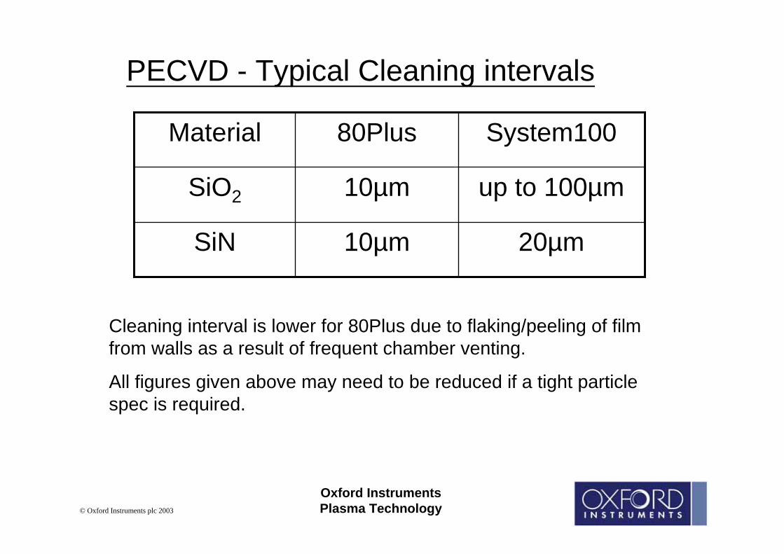
PECVD - Typical Cleaning intervals
20µm10µmSiN
up to 100µm10µmSiO2
System10080PlusMaterial
Cleaning interval is lower for 80Plus due to flaking/peeling of film from walls as a result of frequent chamber venting.
All figures given above may need to be reduced if a tight particle spec is required.
Oxford Instruments Plasma Technology© Oxford Instruments plc 2003
Every 500-1000µm of film it will be necessary to perform a ‘wet clean’as follows:
1) Plasma clean chamber
2) Cool down of electrode (advisable to avoid hot surface hazard)
3) Examine chamber – vacuum any flakes/particles
4) IPA wipe of chamber walls if necessary
5) Dry wipe of showerhead, or beadblast showerhead if necessary
6) Re-install showerhead, pump/purge chamber, and condition
Beadblast using alumina powder (aluminium oxide beads) of 180 grit size or less - maybe 120. Do not use any solvents. Clean the showerhead after beadblasting using compressed air only. Hold the showerhead up to the light to check that none of the holes are blocked by any grit from the beadblasting. Clean out holes with paper clip or similar if blocked.
PECVD – Typical ‘wet clean’ interval

Oxford Instruments Plasma Technology© Oxford Instruments plc 2003
PECVD – showerhead bright spots
It is quite common to see PECVD showerhead holes becoming enlarged. This is caused during high-power processing (on an 80 Plus this is typically during plasma cleaning). Any holes which have slightly sharper edges will form an intense discharge over the hole (due to the high fields generated by the sharper edges). This can be seen as a 'bright spot' in the plasma locatedover the hole during the clean process.
This can cause some erosion of the hole and widening of the hole opening (on the outlet side only). Eventually, the bright spot burning itself out, i.e. the erosion removes the sharp edges and hence the bright spot no longer occurs at that hole. This may happen for several holes during the initial run-up of the system, until the showerhead 'stabilises' itself.The bright spot may also result in some black/brown polymer deposition around the holes which, can cause premature flake-off of deposited films. It is recommended that the showerhead is bead-blasted clean to remove such residues.
The bright spots should not be observed during low power (<50W) 80 Plus deposition processes. If they are, it is recommended that the showerhead is plasma cleaned and bead-blasted cleaned until the bright spots are eliminated. It is sometimes possible to cure the bright spot by using a de-burring tool to clean out any machining residues from the hole in question. If bright spots are still present then it may be necessary to obtain a replacement showerhead.
The effect of the enlarged holes on the deposition results should be minimal, since they only enlarge the outlet of the hole, hence they do not affect the gas flow.