basic tube power supplies - diy audio...
TRANSCRIPT
Power Supply Design for Vacuum Tube AmplifiersMatt Renaud, January 2012
Introduction
It’s time for a little confession: I don’t always spend as much time on my power supply designs as I should. Sometimes I get excited about my latest circuit and after looking for just the right tubes, output transformers, coupling caps, and low noise resistors, the power supply design becomes almost an after thought. Sometimes things turn out ok and there are no problems. Other times I end up with bad voltages, unacceptable power supply sag, channel crosstalk, or worst of all, a hum that I just can’t seem to eliminate. It’s at these times that I always wish I had taken a little more time to get it right.
The truth is, there is no reason to suffer power supply set backs like this. The design of basic tube power supplies is actually very straight forward. And, if we rely on the excellent work of those who’ve come before us (O. H. Schade, N. H. Roberts, D. L Waidelich, H. J. Reich), we don’t even need to tackle any advanced math or taxing mental gyrations to arrive at some truly excellent power supply designs.
What I’d like to do here is to walk through a design process first recommended by O. H. Schade1 in 1943 and presented in a slightly modified version by Herbert Reich in 1944 in his book “Theory and Applications of Electron Tubes”2. Now, the state of electronics has changed somewhat in the 67 years since Schade first published his landmark work. As such, I will present again, a somewhat modified version of this process more suited to today’s amp builders and hobbyists. This process uses only simple equations and Schade’s original graphs as modified by Reich. Even those builders who are unfamiliar or uncomfortable with advanced mathematics should have no problems using this approach. The entire process relies on assuming that the rectifier, when conducting, acts like a resistor. So if you can figure out how this resistance acts at your planned load current, you can get your power supply design just right.
I am going to work through the procedure by designing a supply for a mythical low power stereo amplifier. It’s a stereo single ended class A design I’ll refer to as the Ghost amp. I will first present the process for each step and then fill in some numbers to show how the process works. I urge readers to read the entire design process first and then go back and look closely at the math. It’s not advanced, but it can be a little intimidating the first time through. As I work though the process, I introduce new variables and identify them with unique letters and symbols.
Part 1 - The Basic Power Supply
Power Supply Constraints and Choices
The first step is to determine the total load for your power supply. This is the B+ voltage required by your amp, and the total load current for all plate supply and screen supply voltages. If you are building for a stereo amplifier, be sure to include both channels. I will refer to these as VL and IL respectively.
Page 1 of 21
1 Schade, O. H., Proceedings of the I.R.E, 31, p341-361, (1943)
2 Reich, Herbert J, “Theory and Applications of Electron Tubes”, 2nd Ed., McGraw-Hill, 1944
http://diyaudioprojects.com/Technical/Tube-Power-Supplies/
Also required is the mains voltage and frequency where the amp is to be used. This will affect your transformer selection and your overall power supply design. These I will refer to as VM and fM respectively.
For the Ghost amp, each channel requires a B+ voltage of 250v at 59mA at idle and 65mA at peak output. So VL=250v and IL= 2 *65mA = 130mA. Here in North America the main power is 120v at 60 Hz so VM=120v and fM=60Hz. These will be our starting points. So summarizing, we are starting with the following conditions:
VL = 250vIL = 130mAVM = 120vfM = 60Hz
Now we need to choose a topology. Our basic options are a single diode half wave rectifier, a dual diode full wave rectifier (center tapped transformer secondary), or a dual diode full wave voltage doubler. There are other topologies of course, but these three are the most suitable for high fidelity amplifiers. For the Ghost amp I will choose a full wave dual diode rectifier. This topology has advantages over the half wave circuit in that the ripple is lower and the ripple frequency is twice as high making it easier to filter. The dual diode voltage doubler shares these characteristics but since the required VL is fairly low (by tube amp standards), there is no need to deal with the added complexity of the voltage doubler.
I am also going to choose to use a capacitor input filter. I could also use a choke input filter, however the choke would require a much higher transformer secondary voltage and a larger choke than the capacitor input filter. This would drive up the size and cost of the power supply and small and cheaper is better than large and more expensive.
The First Calculations - Currents and Voltages
Now that we have the basic electrical constraints and have chosen a topology, it’s time to start estimating the electrical parameters which will drive the power supply’s operation. The first of these are the diode plate currents. Once calculated these will allow us to choose a suitable rectifier tube for our amplifier. The average plate current in our full wave rectifier is simply one half the total load current; one half for each diode.
IP = IL
2= 130mA
2= 65mA (eq. 1)
The peak plate current is more complex. Because the input capacitor only partially discharges on each half cycle, the diode can only conduct on that portion of the following cycle when the plate voltage exceeds the voltage to which the capacitor discharged between cycles. This means that the capacitor charging current must be significantly greater than the average plate current. Here we are going to make an assumption. Based on the typical performance of vacuum tube rectifiers we are going to assume that the effective peak charging current per plate is four times the average current. Later we will refine this
Page 2 of 21
http://diyaudioprojects.com/Technical/Tube-Power-Supplies/
estimate based on our preliminary results. So using this estimate yields the following result for the peak plate current.
IP = 4IP = 4 *65mA = 260mA (eq. 2)
Now that we know the peak plate current it is time to choose a rectifier tube. Making this decision requires checking the tube data sheets, looking at max ratings and voltage drops, and applying some judgement and experience. There are some basic rules to apply which make this task easier. First, and most importantly, the maximum tube ratings must not be violated. We already have an estimate of the maximum plate current. But what about the diode peak inverse voltage. The diode will see this voltage when the capacitor is at max voltage, i.e VL, and the transformer winding is at the peak opposite voltage. Since we can’t as yet estimate voltage drop in the rectifier, it is good to assume it’s zero so the peak inverse voltage on the diode will be the load voltage plus the peak AC voltage from half of the center tapped secondary. Since we don’t know our secondary voltage yet we’ll estimate it’s RMS value as the the same as VL. This means that the peak inverse diode voltage will be as follows.
VDi = VL + 2VL = 1+ 2( )VL = 2.41*250v = 603v (eq. 3)
There is one other important parameter which is the diode voltage drop. While the amp is at idle, the voltage drop across each diode will be one voltage, and when the amp is approaching full power the current draw will be greater and the diode voltage drop will be greater. This will result in what is known as power supply sag. For class A operation (such as our Ghost amp), sag is generally not a major consideration (current change is only ~10%), for class AB or B operation, sag can become a major issue. Because we are shooting for a high fidelity amplifier we will want to limit sag as much as possible.
It should be noted that minimizing sag is not always the best design choice. Particularly in guitar amplifiers, power supply sag can create unique distortion and tonal qualities which are actually quite desirable. But for musical reproduction this is not generally the case so, for the Ghost amp, we want to limit sag as much as possible.
Choosing the Rectifier Tube
So, with all these constraints, how do we go about choosing just the right tube for the job? Lets examine the following graph. This is a collection of vacuum tube rectifier voltage drops as a function of plate current. It shows just how much drop there is for each tube and allows us to get a feel for how much sag to expect for a given tube.
Page 3 of 21
http://diyaudioprojects.com/Technical/Tube-Power-Supplies/
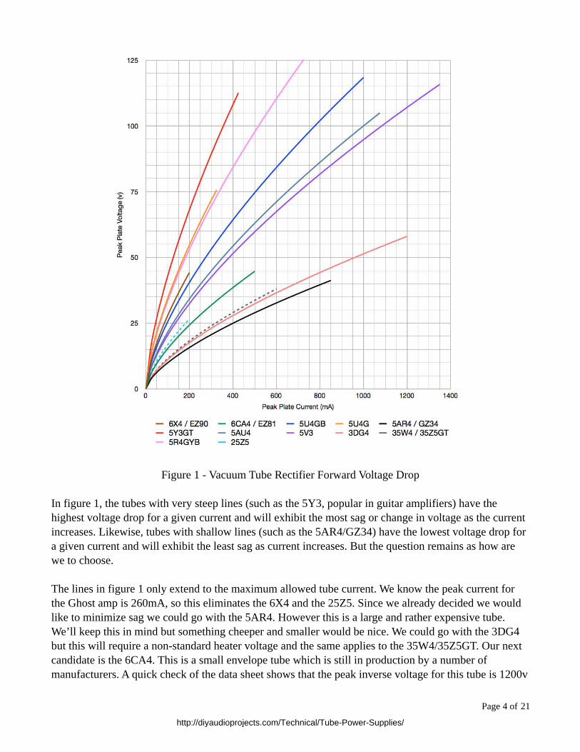
Figure 1 - Vacuum Tube Rectifier Forward Voltage Drop
In figure 1, the tubes with very steep lines (such as the 5Y3, popular in guitar amplifiers) have the highest voltage drop for a given current and will exhibit the most sag or change in voltage as the current increases. Likewise, tubes with shallow lines (such as the 5AR4/GZ34) have the lowest voltage drop for a given current and will exhibit the least sag as current increases. But the question remains as how are we to choose.
The lines in figure 1 only extend to the maximum allowed tube current. We know the peak current for the Ghost amp is 260mA, so this eliminates the 6X4 and the 25Z5. Since we already decided we would like to minimize sag we could go with the 5AR4. However this is a large and rather expensive tube. We’ll keep this in mind but something cheeper and smaller would be nice. We could go with the 3DG4 but this will require a non-standard heater voltage and the same applies to the 35W4/35Z5GT. Our next candidate is the 6CA4. This is a small envelope tube which is still in production by a number of manufacturers. A quick check of the data sheet shows that the peak inverse voltage for this tube is 1200v
Page 4 of 21
http://diyaudioprojects.com/Technical/Tube-Power-Supplies/
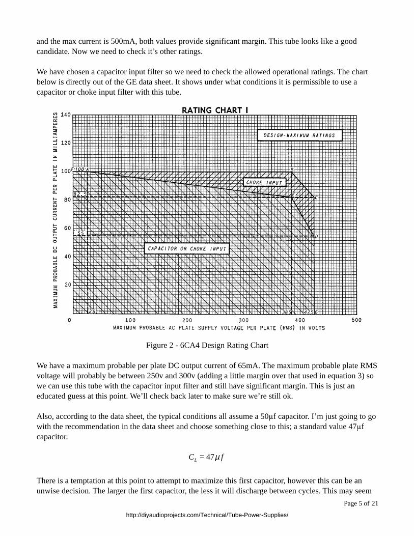
and the max current is 500mA, both values provide significant margin. This tube looks like a good candidate. Now we need to check it’s other ratings.
We have chosen a capacitor input filter so we need to check the allowed operational ratings. The chart below is directly out of the GE data sheet. It shows under what conditions it is permissible to use a capacitor or choke input filter with this tube.
Figure 2 - 6CA4 Design Rating Chart
We have a maximum probable per plate DC output current of 65mA. The maximum probable plate RMS voltage will probably be between 250v and 300v (adding a little margin over that used in equation 3) so we can use this tube with the capacitor input filter and still have significant margin. This is just an educated guess at this point. We’ll check back later to make sure we’re still ok.
Also, according to the data sheet, the typical conditions all assume a 50µf capacitor. I’m just going to go with the recommendation in the data sheet and choose something close to this; a standard value 47µf capacitor.
CL = 47µ f
There is a temptation at this point to attempt to maximize this first capacitor, however this can be an unwise decision. The larger the first capacitor, the less it will discharge between cycles. This may seem
Page 5 of 21
http://diyaudioprojects.com/Technical/Tube-Power-Supplies/
like a good thing (e.g. it reduces ripple voltage), but it means that the conduction angle (that portion of the cycle over which the capacitor recharges) will be much shorter. This will drive up the peak diode current and can lead to either damaging the tube or causing unnecessary voltage drop and excessive transformer heating. Here, smaller is actually better. The total ripple may be higher, but we’ll deal with that in the filter design.
This process of choosing a rectifier tube may seem somewhat arbitrary at this point; and in some aspects it is. However, as designers become more experienced and familiar with the various rectifier tubes, most tend to settle on one or two favorites, and only stray when they really need something different. Now that we have chosen an appropriate tube and input capacitor value, it’s time to begin estimating the performance of our design.
Rectifier Calculations
The first thing we need to do is estimate the peak and average resistances for our rectifier diodes. Since we already have the peak current estimate from equation 2 we can use this along with the voltage drop from figure 1 to calculate the peak diode resistance. From figure 1, for the 6CA4 at 260mA, the forward voltage drop is 28v (This information is also available on the data sheet.). This gives the peak diode resistance as follows.
rp = Vd
IP
= 28v260mA
= 108Ω (eq. 4)
Up to this point we have been making simple calculations based on simple circuit theory and data sheets. Now we need to fall back on some of the work already accomplished by Schade back in 1943. Schade found that the value of the average diode resistance could be calculated (to within an acceptable margin of error) from the peak diode resistance by a simple multiplicative factor. So by following Schade’s solution we get the following.
rp = 1.14rp = 1.14 *108Ω = 123Ω (eq. 5)
Now we need to find the total peak and average resistances which include the effects of the transformer winding resistances. Obviously this presents a slight problem as we haven’t yet chosen a power supply transformer. So again we will have to make an estimate. The effective transformer secondary winding resistance is given by the following equation.
RS = Rsecondary + N 2Rprimary (eq. 6)
where Rsecondary is the secondary winding resistance per section Rprimary is the primary winding resistance and N is the voltage step up ratio per section.
Page 6 of 21
http://diyaudioprojects.com/Technical/Tube-Power-Supplies/
For a modern vacuum tube power transformer, the resistance of a typical secondary winding of 250v to 300v, rated at 150mA, is on the order of 50Ω and the primary may be on the order of 10Ω. If we assume a 250v RMS secondary voltage per section, the voltage step up ratio is as follows:
N =Vsecondary
VM
= 250v120v
= 2.08 (eq. 7)
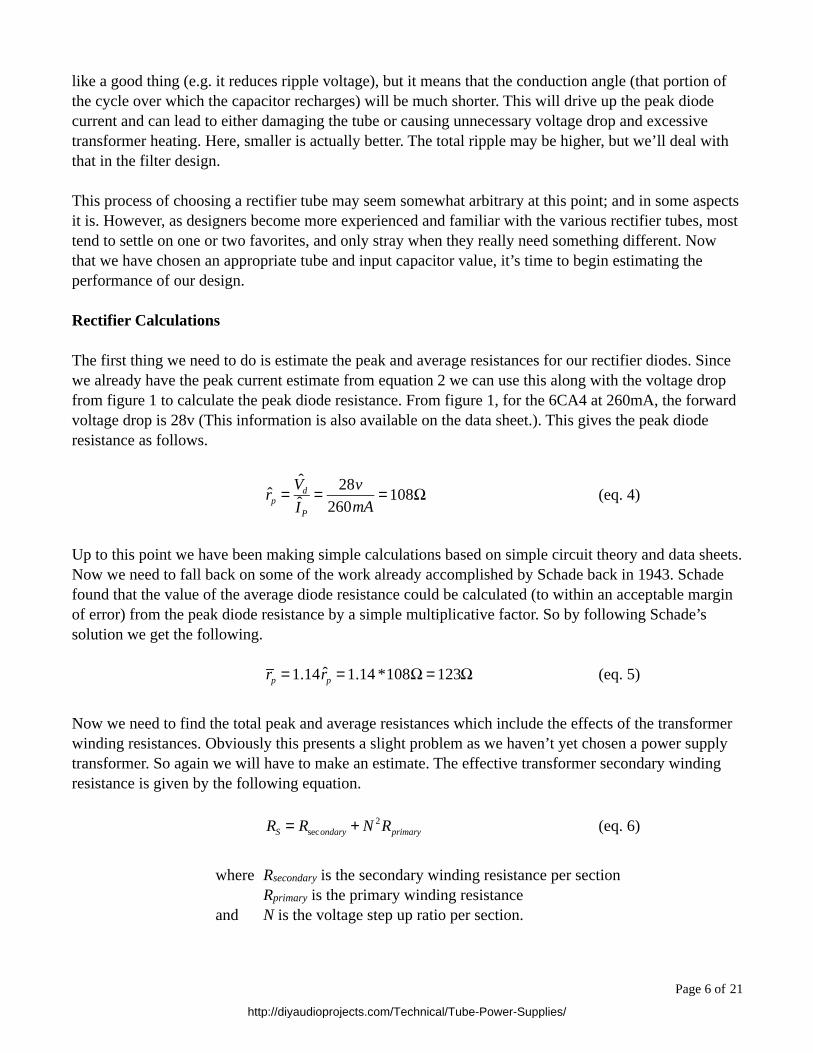
Combining this result with our other estimates, equation 6 yields an effective transformer resistance of ~93Ω per section. At this point it’s a good idea to make a check on our rectifier data sheet for the minimum allowed source resistance. If the source resistance is too low then the initial inrush current to charge the capacitor will exceed the limits of the rectifier. So lets return to the data sheet.
Figure 3 - 6CA4 Source Resistance Rating Chart
According to the graph in Figure 3, at the 250v RMS voltage we assumed previously, the minimum allowed source resistance is ~125Ω. However, if you look at the note on the graph you’ll find that this minimum resistance is only required if “hot switching” is involved. Hot switching is where the high voltage supply is activated after the tube filaments have come to temperature. If we apply the high voltage load at the same time as the filament voltage, then this resistance requirement can be significantly relaxed. So now we have a decision to make. Either we can insert a ~40Ω resistor in series with each plate (which will result in additional loss in our power supply) or we can put a restriction on the design that there will be no high voltage “standby” switch.
Page 7 of 21
http://diyaudioprojects.com/Technical/Tube-Power-Supplies/
In reality, there is almost never a reason to include a standby switch in a piece of audio equipment with a vacuum tube rectifier. As such, we’ll make the decision to leave out the additional resistance and forego using a standby switch in our design. This is another design constraint of which we’ll need to keep track.
Getting back to our 93Ω estimated transformer resistance, we’ll now use this estimate to calculate the total effective values for the peak and average supply resistances. Here we simply add the transformer resistance estimate to those values calculated in equations 4 and 5.
Rs = rp + RS = 108Ω+ 93Ω = 201Ω (eq. 8a)
Rs = rp + RS = 123Ω+ 93Ω = 216Ω (eq. 8b)
There are three more pieces if information we need before we go back to Schade’s work. The first is equivalent load resistance presented by the amplifier RL. This is found by simply dividing the load voltage by the load current. So for the Ghost Amp we have the following:
RL = VL
IL
= 250v130mA
= 1.92kΩ (eq. 9)
The second piece of information we need is a “frequency time constant” for the rectifier load. This is a measure of the effective discharge time in radians for each half cycle and is shown in the graphs as ωRC. It is calculated as follows:
ωRC = 2π fM RLCL = 2*π *60Hz *1.92kΩ*47µ f = 34.0 (eq. 10)
And the final piece of information is the source resistance to load resistance ratios. These will allow us to check some of our previous assumptions, determine the efficiency of the rectifier, and to chose an appropriate transformer. The resistance ratios are found as follows:
Rs RL = 201Ω1.92kΩ
= 0.105 (eq. 11a)
Rs RL = 216Ω1.92kΩ
= 0.112 (eq. 11b)
Now that we have all this information , it’s time to return to Schade (and Reich).
Assumption Check and Iterative Correction
Now that we have initial estimates for all the rectifier data, the first thing we want to do is begin checking some of the assumptions we made along the way. All the way back in equation 2 we made the assumption that the peak diode current was four times the average plate current. I also said that we would refine this estimate base upon our initial results. Now is the time for that refinement. Using the resistance ratio value of equation11a it is now possible to check this initial assumption. Reich reformatted and published Schade’s plots for performing this check.
Page 8 of 21
http://diyaudioprojects.com/Technical/Tube-Power-Supplies/
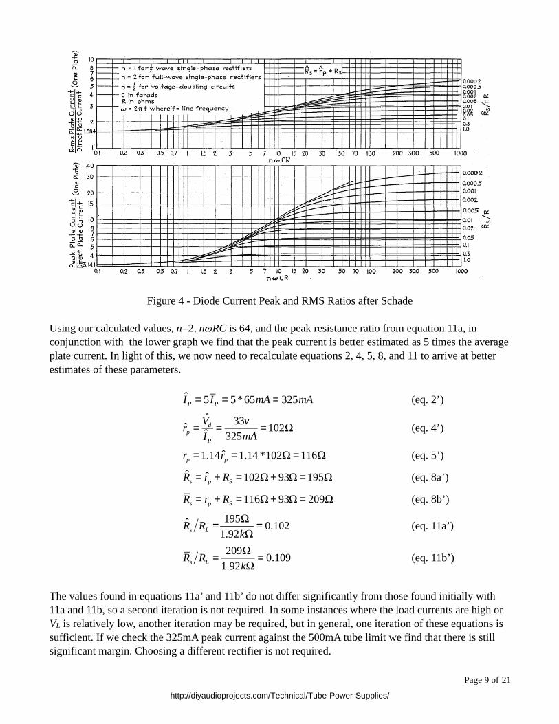
Figure 4 - Diode Current Peak and RMS Ratios after Schade
Using our calculated values, n=2, nωRC is 64, and the peak resistance ratio from equation 11a, in conjunction with the lower graph we find that the peak current is better estimated as 5 times the average plate current. In light of this, we now need to recalculate equations 2, 4, 5, 8, and 11 to arrive at better estimates of these parameters.
IP = 5IP = 5*65mA = 325mA (eq. 2’)
rp = Vd
IP
= 33v325mA
= 102Ω (eq. 4’)
rp = 1.14rp = 1.14 *102Ω = 116Ω (eq. 5’)
Rs = rp + RS = 102Ω+ 93Ω = 195Ω (eq. 8a’)
Rs = rp + RS = 116Ω+ 93Ω = 209Ω (eq. 8b’)
Rs RL = 195Ω1.92kΩ
= 0.102 (eq. 11a’)
Rs RL = 209Ω1.92kΩ
= 0.109 (eq. 11b’)
The values found in equations 11a’ and 11b’ do not differ significantly from those found initially with 11a and 11b, so a second iteration is not required. In some instances where the load currents are high or VL is relatively low, another iteration may be required, but in general, one iteration of these equations is sufficient. If we check the 325mA peak current against the 500mA tube limit we find that there is still significant margin. Choosing a different rectifier is not required.
Page 9 of 21
http://diyaudioprojects.com/Technical/Tube-Power-Supplies/
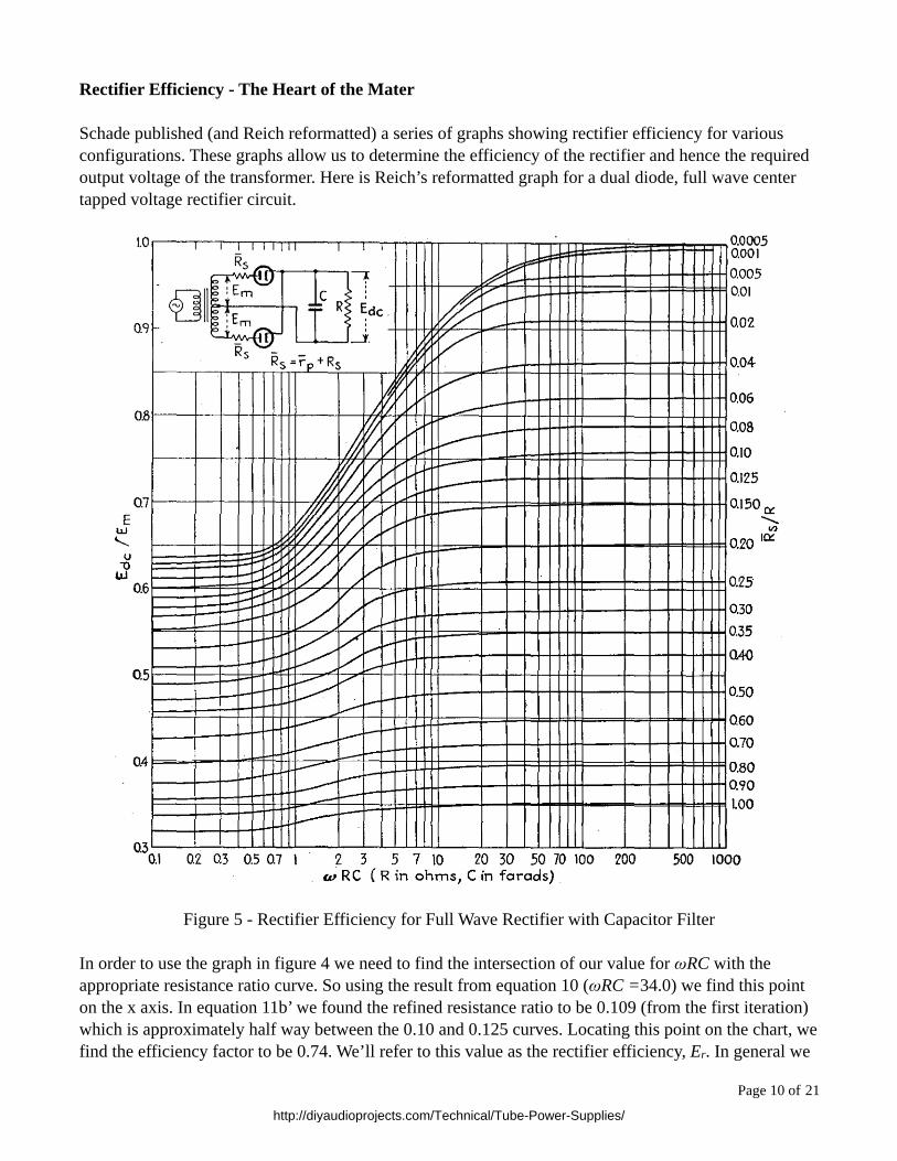
Rectifier Efficiency - The Heart of the Mater
Schade published (and Reich reformatted) a series of graphs showing rectifier efficiency for various configurations. These graphs allow us to determine the efficiency of the rectifier and hence the required output voltage of the transformer. Here is Reich’s reformatted graph for a dual diode, full wave center tapped voltage rectifier circuit.
Figure 5 - Rectifier Efficiency for Full Wave Rectifier with Capacitor Filter
In order to use the graph in figure 4 we need to find the intersection of our value for ωRC with the appropriate resistance ratio curve. So using the result from equation 10 (ωRC =34.0) we find this point on the x axis. In equation 11b’ we found the refined resistance ratio to be 0.109 (from the first iteration) which is approximately half way between the 0.10 and 0.125 curves. Locating this point on the chart, we find the efficiency factor to be 0.74. We’ll refer to this value as the rectifier efficiency, Er. In general we
Page 10 of 21
http://diyaudioprojects.com/Technical/Tube-Power-Supplies/
want the ωRC value from equation 10 to be to the right hand side of the knee in the curves of figure 5. This helps ensure that as the current draw on the supply fluctuates (i.e. the effective RL changes) the efficiency and hence the output voltage remains fairly constant. This is referred to a good load regulation.
What the rectifier efficiency really means is that the ratio of the DC output voltage, Edc, to the peak transformer secondary voltage per section, Em, (or 1.414 times the RMS secondary voltage) is 0.74. This is shown mathematically as follows.
Er = Edc
EM
(eq. 12)
Reformatting equation 12 allows us to determine the required transformer peak secondary voltage per section.
EM = Edc
Er
= 250v0.74
= 338v (eq. 13)
To find the required RMS secondary voltage per section we simply divide the peak voltage by the square root of 2.
ERMS = EM
2= 338v
1.414= 239v (eq. 14)
Before we go forward, it’s time to make one more check on our rectifier data sheet. From our calculated data and figure 5 we determined that the rectifier efficiency was 0.74. We need to check if this is acceptable. The following is the efficiency rating chart from the 6CA4 data sheet.
Page 11 of 21
http://diyaudioprojects.com/Technical/Tube-Power-Supplies/
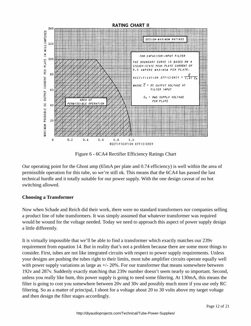
Figure 6 - 6CA4 Rectifier Efficiency Ratings Chart
Our operating point for the Ghost amp (65mA per plate and 0.74 efficiency) is well within the area of permissible operation for this tube, so we’re still ok. This means that the 6CA4 has passed the last technical hurdle and it totally suitable for our power supply. With the one design caveat of no hot switching allowed.
Choosing a Transformer
Now when Schade and Reich did their work, there were no standard transformers nor companies selling a product line of tube transformers. It was simply assumed that whatever transformer was required would be wound for the voltage needed. Today we need to approach this aspect of power supply design a little differently.
It is virtually impossible that we’ll be able to find a transformer which exactly matches our 239v requirement from equation 14. But in reality that’s not a problem because there are some more things to consider. First, tubes are not like integrated circuits with respect to power supply requirements. Unless your designs are pushing the tubes right to their limits, most tube amplifier circuits operate equally well with power supply variations as large as +/- 20%. For our transformer that means somewhere between 192v and 287v. Suddenly exactly matching that 239v number doesn’t seem nearly so important. Second, unless you really like hum, this power supply is going to need some filtering. At 130mA, this means the filter is going to cost you somewhere between 20v and 30v and possibly much more if you use only RC filtering. So as a matter of principal, I shoot for a voltage about 20 to 30 volts above my target voltage and then design the filter stages accordingly.
Page 12 of 21
http://diyaudioprojects.com/Technical/Tube-Power-Supplies/
Now you may be thinking that we set VL as 250v right at the start. How can it be ok to simply increase the voltage 20v to 30v without rerunning all the equations? The answer to this question lies in the percentage change I am assuming (~12%) which is fairly small and in how VL affects the calculations. Increasing the output voltage while maintaining the current draw increases the rectifier peak inverse voltage (equation 3), but a quick check shows plenty of margin so that shouldn’t be a problem. It increases the transformer voltage step up ratio and hence the effective secondary resistance by about 11Ω (equations 6 and 7) increasing the total source resistances in equation 8. It also increases the effective load resistance calculated in equation 9 (to 2.15kΩ). However, in the efficiency numbers calculated in equation 11, these increases tend to offset each other so the overall effect on the resistance ratios and hence rectifier efficiency is small. In reality, a 20v to 30v change on top of a 250v supply is really not much of a change at all.
If you have any questions, then you should rerun the numbers to convince yourself. With practice and experience you’ll begin to get a feel for how different parameters affect the design point and rerunning the equations usually won’t be required.
So now we want a transformer with a secondary voltage of somewhere between 259v and 269v RMS per section or between 518v and 538v RMS for the entire secondary. A quick check of a suppliers website quickly shows that this is not a very common voltage range. However what is a common voltage is 550v or 275v RMS per section. So, we settle on this voltage and will if we need to slightly reduce the voltage, we’ll add a dropping resistor in the filter.
Assessing the Design So Far
So where does all this calculation leave us? Returning to equation 12, we can rearrange the equation to get the dc output voltage as a function of the peak secondary voltage per section. Also, by rearranging equation 14 we can express the peak voltage as a function of the RMS voltage. By combing the two we arrive at our output voltage as follows:
Edc = 2ERMSEr = 1.414 *275v*0.74 = 288v (eq. 15)
This voltage is 38v higher than our target voltage of 250v. However, this is all right as it gives us some voltage drop to apply to our smoothing filter.
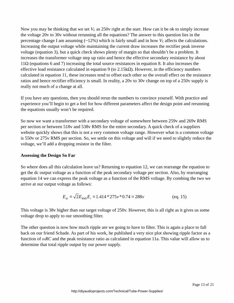
The other question is now how much ripple are we going to have to filter. This is again a place to fall back on our friend Schade. As part of his work, he published a very nice plot showing ripple factor as a function of ωRC and the peak resistance ratio as calculated in equation 11a. This value will allow us to determine that total ripple output by our power supply.
Page 13 of 21
http://diyaudioprojects.com/Technical/Tube-Power-Supplies/
Figure 7 - Ripple Factor for Capacitor Loaded Rectifier Circuits
Using our value of ωRC from equation 10 (34) and the peak resistance ration from equation 11a’ (0.102) we determine that the ripple factor, rf, is approximately 0.018. Using this information the total ripple for our supply is calculated as follows:
Vr = rf Edc = 0.018*288v = 5.18v (eq. 16)
This level of ripple may look high, however it is actually very typical of this type of power supply design. I consider this an excellent result for input to our smoothing filter.
Part 1 Summary
So summarizing our design we have a supply utilizing a transformer 550vct secondary, a 6CA4 rectifier tube, and a 47µf input capacitor. Load regulation is good and we have ample rectifier margin to ensure good operation and long tube life. Supply hot switching will not be utilized to minimize inrush currents at startup. Our output voltage is 288v going into the smoothing filter leaving 38v for filter voltage losses therein. Our ripple going into the filter is 5.18v (1.8%) or approximately -35dBv below the operating voltage. This is a good design solution.
In the next section we’ll be discussing the smoothing filter. This will take the output of our basic power supply and make it suitable for feeding our high fidelity Ghost amp.
Page 14 of 21
http://diyaudioprojects.com/Technical/Tube-Power-Supplies/
Part 2 - The Smoothing Filter
Setting the Filter Requirements
Once the rectifier portion of the supply is complete, it’s time to begin thinking about the filter. The most obvious question at this point is “How much filter do I really need?” Unfortunately there is no easy answer to this question. The answer is going to depend on the type of load on the supply and how it’s going to be used. A stereo amplifier requires more filtering than a mono-block design. A class A output stage requires less filtering than a class AB output stage. So we are going to need to set some simplifying assumptions.
In chapter 14 of his book “Theory and Applications of Electron Tubes”, Herbert Reich gives some good rules of thumb for just how much ripple may be acceptable for various types of circuits. Based on Reich’s recommendation I generally require a B+ voltage ripple level of at least -90dBv or about 0.0031% for any general purpose audio amplifier such as the Ghost amp. So this is where we’ll start with our filter design.
Smoothing Factors
When dealing with power supply filters it is generally easiest to talk in terms of smoothing factors. A smoothing factor is simply a numeric factor for how much the ripple is reduced. For example, a smoothing factor of 100 will reduce 5 volts of ripple to 0.05 volts of ripple. Another way to think about this is that the smoothing factor in dBv subtracted from the power supply ripple level in dBv gives the overall ripple level at the filter output.
As an example, the output of out ghost amp power supply was 288v with 5.18v rms of ripple. This yields a ripple level of -35dBv. In order to achieve our ripple target of -90dBv we’ll need another -55dBv of ripple reduction from our filter or a total smoothing factor of 562. The smoothing factor and it’s dBv equivalent are related by the following relation.
Fs dBv( ) = 20 log Fs( ) = 20 log 562( ) = 55dBv (eq. 17a)
FS = 10FS dBv( )
20⎛⎝⎜
⎞⎠⎟ = 10
55dBv20( ) = 562 (eq. 17b)
Filter Topologies
There are many possible filter topologies which may be used to achieve the required ripple reduction. They may be passive or active, single or multi-stage, and closed or open loop. For simplicity’s sake, I will only be addressing two types of passive filter stages; the RC filter stage and the LC filter stage. Now a DC power supply filter is a simple circuit which takes advantage of the frequency dependent impedance characteristic of capacitors and/or inductors to separate the AC ripple from the DC supply voltage. Also, one of the real beauties of filter stages in that smoothing factors for cascaded stages are multiplicative. So if you have three cascaded filter stages with smoothing factors of FS1, FS2, and FS3, then the total smoothing factor is given by the following relation.
Page 15 of 21
http://diyaudioprojects.com/Technical/Tube-Power-Supplies/
FST = FS1 × FS2 × FS3 (eq. 18)
The only catch is that equation 18 only holds if in each stage the reactance of the series impedance element at the primary ripple frequency is about 20 times the reactance of the shunt element at the same frequency. Normally this isn’t a problem but it is one thing that we’ll have to check later. With these thoughts in mind, lets look at the two types of filter stages stages mentioned above.
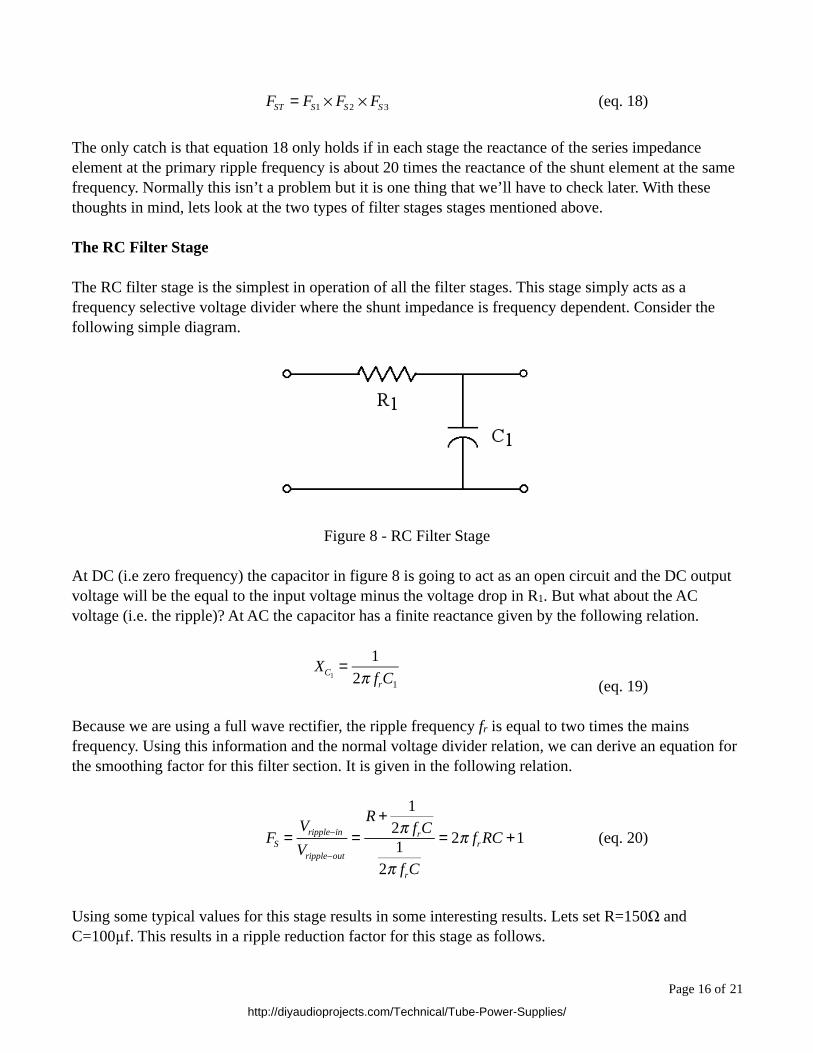
The RC Filter Stage
The RC filter stage is the simplest in operation of all the filter stages. This stage simply acts as a frequency selective voltage divider where the shunt impedance is frequency dependent. Consider the following simple diagram.
Figure 8 - RC Filter Stage
At DC (i.e zero frequency) the capacitor in figure 8 is going to act as an open circuit and the DC output voltage will be the equal to the input voltage minus the voltage drop in R1. But what about the AC voltage (i.e. the ripple)? At AC the capacitor has a finite reactance given by the following relation.
XC1
= 12π frC1 (eq. 19)
Because we are using a full wave rectifier, the ripple frequency fr is equal to two times the mains frequency. Using this information and the normal voltage divider relation, we can derive an equation for the smoothing factor for this filter section. It is given in the following relation.
FS =Vripple−in
Vripple−out
=R + 1
2π frC1
2π frC
= 2π frRC +1 (eq. 20)
Using some typical values for this stage results in some interesting results. Lets set R=150Ω and C=100µf. This results in a ripple reduction factor for this stage as follows.
Page 16 of 21
http://diyaudioprojects.com/Technical/Tube-Power-Supplies/
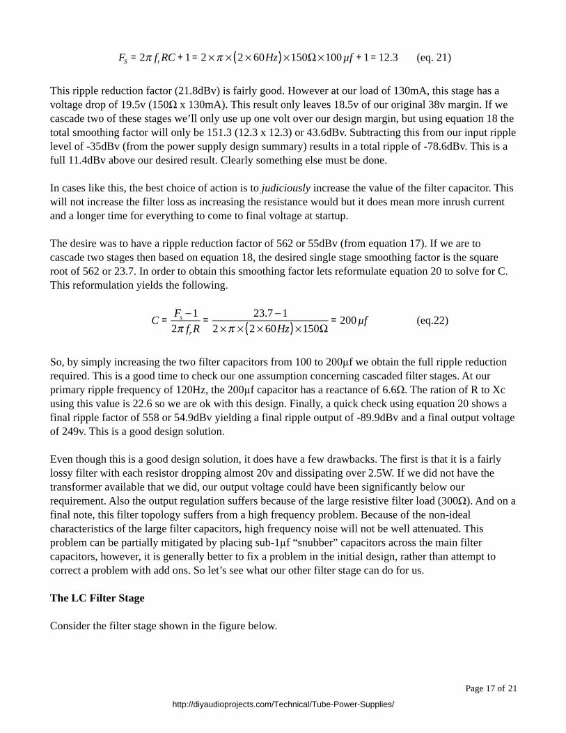
FS = 2π frRC +1 = 2 ×π × 2 × 60Hz( )×150Ω×100µf +1 = 12.3 (eq. 21)
This ripple reduction factor (21.8dBv) is fairly good. However at our load of 130mA, this stage has a voltage drop of 19.5v (150Ω x 130mA). This result only leaves 18.5v of our original 38v margin. If we cascade two of these stages we’ll only use up one volt over our design margin, but using equation 18 the total smoothing factor will only be 151.3 (12.3 x 12.3) or 43.6dBv. Subtracting this from our input ripple level of -35dBv (from the power supply design summary) results in a total ripple of -78.6dBv. This is a full 11.4dBv above our desired result. Clearly something else must be done.
In cases like this, the best choice of action is to judiciously increase the value of the filter capacitor. This will not increase the filter loss as increasing the resistance would but it does mean more inrush current and a longer time for everything to come to final voltage at startup.
The desire was to have a ripple reduction factor of 562 or 55dBv (from equation 17). If we are to cascade two stages then based on equation 18, the desired single stage smoothing factor is the square root of 562 or 23.7. In order to obtain this smoothing factor lets reformulate equation 20 to solve for C. This reformulation yields the following.
C = Fs −12π frR
= 23.7 −12 ×π × 2 × 60Hz( )×150Ω
= 200µf (eq.22)
So, by simply increasing the two filter capacitors from 100 to 200µf we obtain the full ripple reduction required. This is a good time to check our one assumption concerning cascaded filter stages. At our primary ripple frequency of 120Hz, the 200µf capacitor has a reactance of 6.6Ω. The ration of R to Xc using this value is 22.6 so we are ok with this design. Finally, a quick check using equation 20 shows a final ripple factor of 558 or 54.9dBv yielding a final ripple output of -89.9dBv and a final output voltage of 249v. This is a good design solution.
Even though this is a good design solution, it does have a few drawbacks. The first is that it is a fairly lossy filter with each resistor dropping almost 20v and dissipating over 2.5W. If we did not have the transformer available that we did, our output voltage could have been significantly below our requirement. Also the output regulation suffers because of the large resistive filter load (300Ω). And on a final note, this filter topology suffers from a high frequency problem. Because of the non-ideal characteristics of the large filter capacitors, high frequency noise will not be well attenuated. This problem can be partially mitigated by placing sub-1µf “snubber” capacitors across the main filter capacitors, however, it is generally better to fix a problem in the initial design, rather than attempt to correct a problem with add ons. So let’s see what our other filter stage can do for us.
The LC Filter Stage
Consider the filter stage shown in the figure below.
Page 17 of 21
http://diyaudioprojects.com/Technical/Tube-Power-Supplies/
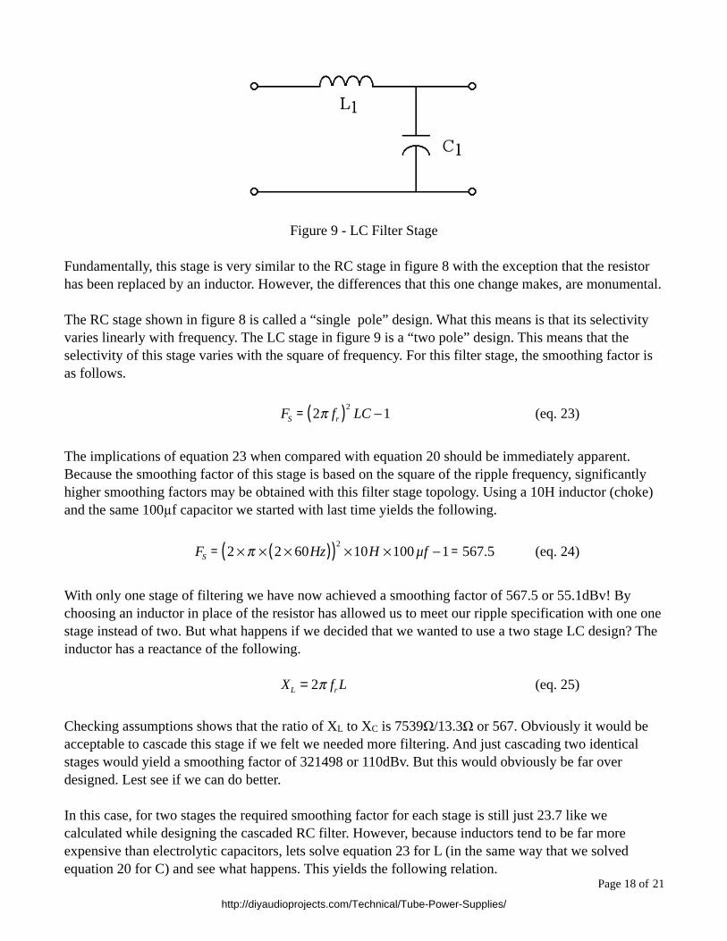
Figure 9 - LC Filter Stage
Fundamentally, this stage is very similar to the RC stage in figure 8 with the exception that the resistor has been replaced by an inductor. However, the differences that this one change makes, are monumental.
The RC stage shown in figure 8 is called a “single pole” design. What this means is that its selectivity varies linearly with frequency. The LC stage in figure 9 is a “two pole” design. This means that the selectivity of this stage varies with the square of frequency. For this filter stage, the smoothing factor is as follows.
FS = 2π fr( )2 LC −1 (eq. 23)
The implications of equation 23 when compared with equation 20 should be immediately apparent. Because the smoothing factor of this stage is based on the square of the ripple frequency, significantly higher smoothing factors may be obtained with this filter stage topology. Using a 10H inductor (choke) and the same 100µf capacitor we started with last time yields the following.
FS = 2 ×π × 2 × 60Hz( )( )2×10H ×100µf −1 = 567.5 (eq. 24)
With only one stage of filtering we have now achieved a smoothing factor of 567.5 or 55.1dBv! By choosing an inductor in place of the resistor has allowed us to meet our ripple specification with one one stage instead of two. But what happens if we decided that we wanted to use a two stage LC design? The inductor has a reactance of the following.
XL = 2π frL (eq. 25)
Checking assumptions shows that the ratio of XL to XC is 7539Ω/13.3Ω or 567. Obviously it would be acceptable to cascade this stage if we felt we needed more filtering. And just cascading two identical stages would yield a smoothing factor of 321498 or 110dBv. But this would obviously be far over designed. Lest see if we can do better.
In this case, for two stages the required smoothing factor for each stage is still just 23.7 like we calculated while designing the cascaded RC filter. However, because inductors tend to be far more expensive than electrolytic capacitors, lets solve equation 23 for L (in the same way that we solved equation 20 for C) and see what happens. This yields the following relation.
Page 18 of 21
http://diyaudioprojects.com/Technical/Tube-Power-Supplies/
L = FS +12π fr( )2 C
(eq. 26)
If we plug in values from our design we get this.
23.7 +12 ×π × 2 × 60Hz( )( )2
×100µf= 0.43H (eq 27)
This is a fairly small inductor so lets check our assumptions. Using equation 25 the inductive reactance XL is 327Ω. so the ratio of XL to XC is 327Ω/13.3Ω or 24.6. Clearly it should be ok to cascade two stages like this to get our required filtering.
A common misconception is that to build a power supply filter with a choke requires a really big one; 10H or more. However we have just shown that this is not the case. Additionally, as I write this, at one vendor I priced a Hammond 10H, 200mA choke at $52.45 USD. However, two 1.5H, 200mA chokes are only $14.90 USD each for a total of $29.80 USD. A net savings of $22.65 or 43%. So lets see how the two filters would compare.
The first filter we already know from equation 24 that it gives a smoothing factor of 567.5 or 55.1dBv. But what about a two stage filter using those 1.5H chokes and 100µf capacitors? The individual smoothing factor is calculated as follows:
FS = 2 ×π × 2 × 60Hz( )( )2×1.5H ×100µf −1 = 84.3 (eq. 28)
So the combined smoothing factor is 84.3 squared or 7106.5 or 77dBv. Not only is this two stage filter cheaper (even though we did need to buy another 100µf capacitor) it provides almost 22dBv lower ripple than the single stage design.
The Final Design
So, where does this leave us with our Ghost Amp power supply. Lets summarize.
At the end of section one we had a 550vct transformer secondary feeding a full wave bridge 6CA4 rectifier tube with a 47µf capacitor. It output 288v at 130mA load. In section two we explored filter topologies and actually designed three which were suitable. But how to choose one.
If we were choosing totally on cost, the cascaded RC filter would be the way to go. If we want the simplest, we’d go with the single LC section to get everything in a simple filter. But I think the mid range solution is best. It has the highest filtering, is not over complicated (only four components) and has the best filtration characteristics of the three. So this is what I’ll choose.
Page 19 of 21
http://diyaudioprojects.com/Technical/Tube-Power-Supplies/
Now there is one more thing to check. We currently have 288v at the input to our filter. A quick check of the inductor data sheets tells us that each 1.5H choke has a series resistance of 56Ω. Therefore the two together have 112Ω. At our specified load of 130mA this lowers the voltage by 112Ωx130mA≈14.5v. Using this loss, the total output voltage of our supply at load is 288v-14.5v or 273.5v. This is 23.5v or 9.4% above the target voltage for the supply.
There are a few ways to deal with this situation. The first is to do nothing. A less than 10% variation in the power supply voltage is not that much. A quick check of the circuit could be made and if it doesn’t result in an over voltage condition on any tubes, then we can leave it as is.
The second approach is to go back to our design process and add additional resistance in line with the plates in the rectifier. We would need to drop 23.5v at the peak current draw per plate which, according to equation 2’ is 325mA. So we would need two resistors of 23.5v/325mA = 72Ω. A 75Ω resistor in each leg would be fine. This approach actually is probably the best technical solution because it lowers peak surge current through the rectifier, lower transformer core heating and provides the best approach for good load regulation.
The third approach is to simply add some series resistance at some point following the first capacitor after the rectifier. This solution has the benefit of actually getting the voltage down to the desired level and is relatively simple. The only question is where to put the resistor. If the filter performance were marginal, I would suggest putting the resistor following the filter and then follow it with another shunt capacitor. In effect, adding an additional RC stage to the filter. This improves the filtering but also has a negative impact on overall load regulation of the supply. Putting the resistor between the first capacitor and the first inductor also lowers the voltage to the desired point but provides better load regulation so this is what we’ll choose. We’ll need a resistor of 23.5v/130mA = 194.6Ω. A 200Ω resistor should work just fine. It’s power dissipation will be 130mAx130mA*200Ω or 3.4W. We’ll chose a 5W for margin.
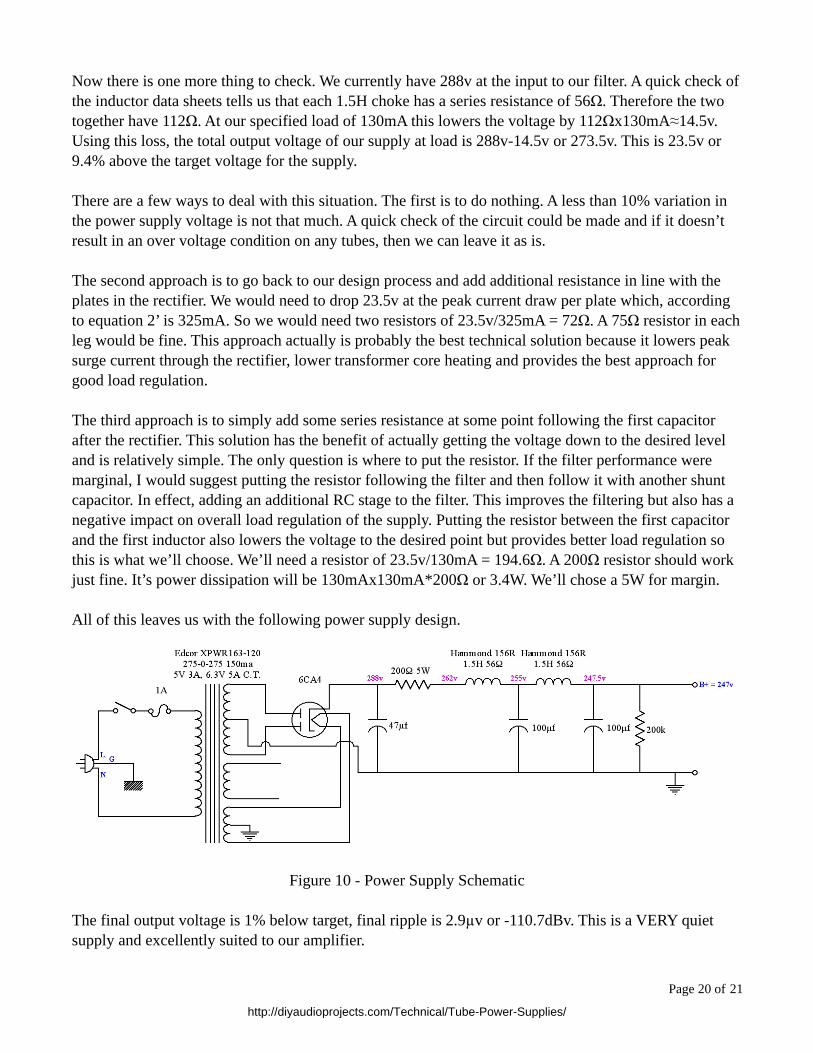
All of this leaves us with the following power supply design.
Figure 10 - Power Supply Schematic
The final output voltage is 1% below target, final ripple is 2.9µv or -110.7dBv. This is a VERY quiet supply and excellently suited to our amplifier.
Page 20 of 21
http://diyaudioprojects.com/Technical/Tube-Power-Supplies/
Conclusion
So where does all this leave us? Well, we’ve shown that with some plots and a little simple arithmetic we can get excellent results. We’ve also developed a simple straight forward method that most people should be able to use every time they need to build a power supply. This is in no way an exhaustive discussion on the topic, but it is a good practical start.
I hope that this discussion takes away some of the mystery surrounding vacuum tube power supplies. And I hope that you’ll feel more comfortable with the topic the next time you decide to build or rebuild an amplifier.
Page 21 of 21
http://diyaudioprojects.com/Technical/Tube-Power-Supplies/