bee403 linear integrated circuits...bee403 linear integrated circuits unit i integrated circuits...
TRANSCRIPT
BEE403 LINEAR INTEGRATED CIRCUITS
UNIT I
INTEGRATED CIRCUITS
Integrated Circuits : An integrated circuit (IC) is a miniature, low cost electronic circuit consisting of active and passive components fabricated together on a single crystal of silicon. The active components are transistors and diodes and passive components are resistors and capacitors.
Classification of ICs (Integrated Circuits)
Below is the classification of different types of ICs basis on their chip size. SSI: Small scale integration. 3 – 30 gates per chip. MSI: Medium scale integration. 30 – 300 gates per chip. LSI: Large scale integration. 300 – 3,000 gates per chip. VLSI: Very large scale integration. More than 3,000 gates per chip.
Types of ICs (Integrated Circuits)
Based on the method or techniques used in manufacturing them, types of ICs can be divided into three classes:
1. Thin and thick film ICs
2. Monolithic ICs
3. Hybrid or multichip ICs
Below is the simple explanation of different types of ICs as mentioned above.
Thin and Thick ICs:
In thin or thick film ICs, passive components such as resistors, capacitors are integrated but the diodes and transistors are connected as separate components to form a single and a complete circuit. Thin and thick ICs that are produced commercially are merely the combination of integrated and discrete (separate) components.
Monolithic ICs
In monolithic ICs, the discrete components, the active and the passive and also the interconnections between then are formed on a silicon chip. The word monolithic is actually derived from two Greek words “mono” meaning one or single and Lithos meaning stone. Thus monolithic circuit is a circuit that is built into a single crystal.

Hybrid or Multi chip ICs
As the name implies, “Multi”, more than one individual chips are interconnected. The active components that are contained in this kind of ICs are diffused transistors or diodes. The passive components are the diffused resistors or capacitors on a single chip
Advantages of ICs
ICs have advantages over those that are made by interconnecting discrete components some of which are its small size.
It is a thousand times smaller than the discrete circuits. It is an all in one (components and the interconnections are on a single silicon chip). It has little weight.
Its cost of production is also low.
It is reliable because there is no soldered joints.
ICs consumes little energy and can easily be replaced when the need arises.
It can be operated at a very high temperature.
Applications of ICs
Different types of ICs are widely applied in our electrical devices such as high power amplifiers, voltage regulators, TV receivers and computers etc.
Operational Amplifier General Conditions
• The Operational Amplifier, or Op-amp as it is most commonly called, can be an ideal amplifier with infinite Gain and Bandwidth when used in the Open-loop mode with typical DC gains of well over 100,000 or 100dB.
• The basic Op-amp construction is of a 3-terminal device, 2-inputs and 1-output, (excluding power connections).
• An Operational Amplifier operates from either a dual positive ( +V ) and an corresponding negative ( -V ) supply, or they can operate from a single DC supply voltage.
• The two main laws associated with the operational amplifier are that it has an infinite input impedance, ( Z = ∞ ) resulting in “No current flowing into either of its two inputs” and zero input offset voltage “V1 = V2“.

• An operational amplifier also has zero output impedance, ( Z = 0 ).
• Op-amps sense the difference between the voltage signals applied to their two input terminals and then multiply it by some pre-determined Gain, ( A ).
• This Gain, ( A ) is often referred to as the amplifiers “Open-loop Gain”.
• Closing the open loop by connecting a resistive or reactive component between the output and one input terminal of the op-amp greatly reduces and controls this open-loop gain.
• Op-amps can be connected into two basic configurations, Inverting and Non-inverting.
The Two Basic Operational Amplifier Circuits
For negative feedback, were the fed-back voltage is in “anti-phase” to the input the overall gain of the amplifier is reduced.
For positive feedback, were the fed-back voltage is in “Phase” with the input the overall gain of the amplifier is increased.
By connecting the output directly back to the negative input terminal, 100% feedback is achieved resulting in a Voltage Follower (buffer) circuit with a constant gain of 1 (Unity).
Changing the fixed feedback resistor ( Rƒ ) for a Potentiometer, the circuit will have Adjustable Gain.
Op amp Pin configuration
The pin configuration of op amp is as follows

Where pins 1 and 5showing Offset Null’s along with potentiometer arrangement
are used to nullify offset voltages. Positive offsets are nullified with pin 1 and
negative offsets are nullified using pin 5.+Vcc and -Vcc are positive and negative
supply voltages respectively generally within a range of + or _12 to + or – 24 .
Pins 2 and 3 are inverting and non inverting input terminals respectively.
Maximum differential input voltages will be specified in datasheets which should
be exceeded, Opamp may get damaged due to high power dissipation. Pin 6 is
single ended output terminal from which output will be taken.
Characteristics of 741 Opamp
Typical Characteristics of 741 opamp for general purpose at T=25 Deg C,
Supply voltage around 12 volts
Operating temperature range 0 degrees to 70 degrees for military grade it
is -55 to 130 Deg C
Vcc of the range + or -18 with Output Voltage swing with load resistance
10 kilo ohms + or -14 volts
Maximum power consumption (dissipated in opamp) around 80 milli watts
Slew rate 0.5 volt/micro second
Input Resistance 2 mega ohms
Output resistance 75 ohms
CMMR (90 db) i.e differential gain/Common mode gain= 31600
Offset voltage 7 milli volts

Offset current 20-200 nano amps maximum
Input Bias Current 80-500 nano amps maximum
Ideal Op amp characteristics
Ideal operational amplifier are characterized by
Infinite gain
Infinite input resistance
Zero output resistance (order of 10’s of ohms)
Infinite bandwidth (practically restricted by slew rate)
Linear irrespective of entire analog signal range No offsets and, so on
Definition of Differential Amplifier
A differential amplifier is one which amplifies only difference between two
signals. Ideally difference amplifier should not amplify signal content common to
both input signals. Practically the common mode signal gain will be finite. The
efficiency of differential amplifier is quantified in terms of parameter called
Common Mode Rejection Ratio. Common Mode Rejection Ratio of an differential
amplifier is defined as follows
CMMR = 20 * log10 (Ad/Ac)
Where,
Ad is differential mode signal gain
Ac is common mode signal gain.
Need for differential amplifier
Consider a transducer which provides a small signal at its output terminals which
has to be sent to the measuring instrument. The medium carrying these signals
for example copper wire may induce an interference signal which is comparable
or larger than the transducer output signal. This noise signal is common to both
output terminals. Hence by using differential amplifier at the front end of the
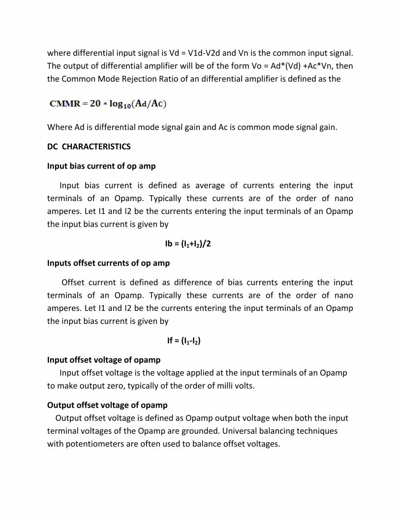
amplifier this noise signal can be attenuated to a large extent so that its
amplitude is negligible to the transducer output signal.
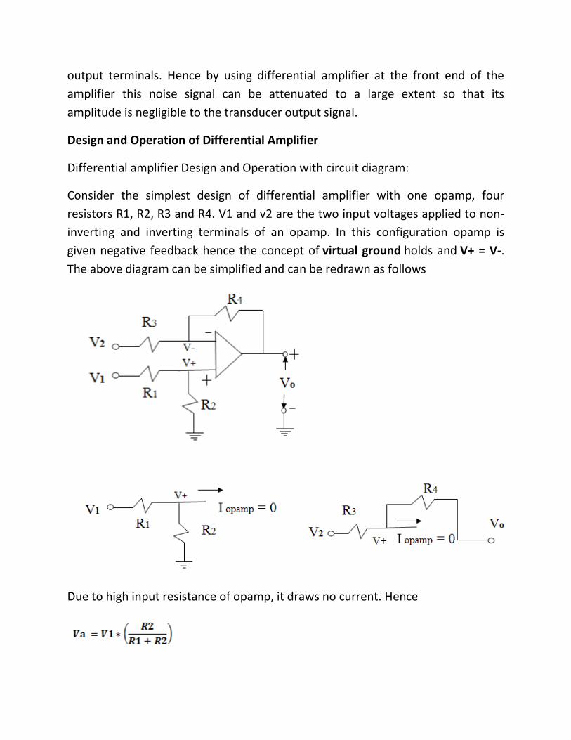
Design and Operation of Differential Amplifier
Differential amplifier Design and Operation with circuit diagram:
Consider the simplest design of differential amplifier with one opamp, four
resistors R1, R2, R3 and R4. V1 and v2 are the two input voltages applied to non-
inverting and inverting terminals of an opamp. In this configuration opamp is
given negative feedback hence the concept of virtual ground holds and V+ = V-.
The above diagram can be simplified and can be redrawn as follows
Due to high input resistance of opamp, it draws no current. Hence
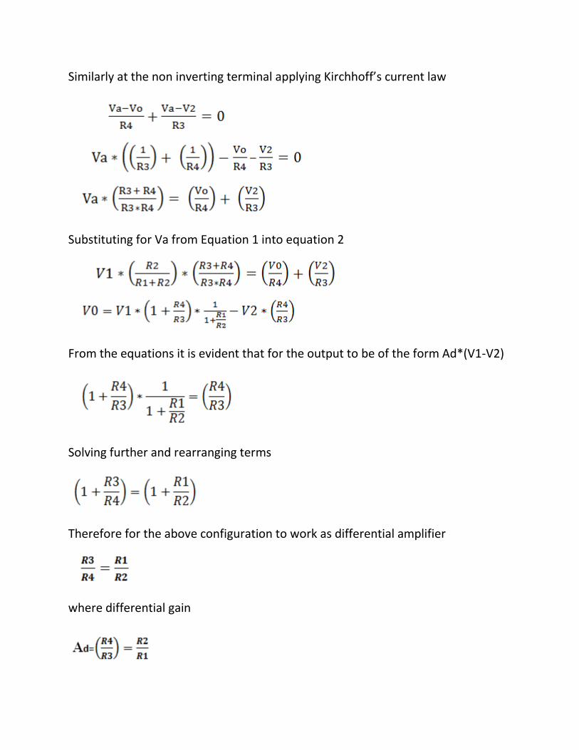
Similarly at the non inverting terminal applying Kirchhoff’s current law
Substituting for Va from Equation 1 into equation 2
From the equations it is evident that for the output to be of the form Ad*(V1-V2)
Solving further and rearranging terms
Therefore for the above configuration to work as differential amplifier
where differential gain

Common Mode Gain of Differential Amplifier
Assume that the resistors are not perfectly matched and let V1=V1d+Vn and
V2=V2d+Vn where differential input signal is Vd = V1d-V2d and Vn is the common
input signal. From equation 3 by substituting equations for V1 and V2 we get
Disadvantages of Differential Amplifier
1. If the Resistors are selected in such a way that the differential gain of amplifier
is high (R1 is selected to have less value compared to R2) then the input
resistance of the amplifier will be less.
2. It is difficult to manipulate differential gain since if we change resistance in one
branch then we need to change resistance in other branch so that the
condition is satisfied.
Slew rate of op amp
It is the maximum rate at which output can change in an opamp. It is one of
the major limitations in an opamp. It is expressed in volt/second. The output gets
distorted if the rate at which output changes exceeds slew rate.
Consider a opamp with slew rate specified in manufacturers datasheet as 10
v/microsecond if we apply a sine wave with frequency w and amplitude A
maximum product A*W*gain can be at most 10v/microsecond before opamp
input output characteristics steps into nonlinear regime.
CMRR of op amp
CMMR is acronym for Common Mode Rejection Ration which is used to
quantify how good a differential amplifier is. Let V1=V1d+Vn and V2=V2d+Vn
where differential input signal is Vd = V1d-V2d and Vn is the common input signal.
The output of differential amplifier will be of the form Vo = Ad*(Vd) +Ac*Vn, then
the Common Mode Rejection Ratio of an differential amplifier is defined as the
Where Ad is differential mode signal gain and Ac is common mode signal gain.
DC CHARACTERISTICS
Input bias current of op amp
Input bias current is defined as average of currents entering the input
terminals of an Opamp. Typically these currents are of the order of nano
amperes. Let I1 and I2 be the currents entering the input terminals of an Opamp
the input bias current is given by
Ib = (I1+I2)/2
Inputs offset currents of op amp
Offset current is defined as difference of bias currents entering the input
terminals of an Opamp. Typically these currents are of the order of nano
amperes. Let I1 and I2 be the currents entering the input terminals of an Opamp
the input bias current is given by
If = (I1-I2)
Input offset voltage of opamp
Input offset voltage is the voltage applied at the input terminals of an Opamp
to make output zero, typically of the order of milli volts.
Output offset voltage of opamp
Output offset voltage is defined as Opamp output voltage when both the input
terminal voltages of the Opamp are grounded. Universal balancing techniques
with potentiometers are often used to balance offset voltages.

Inverting amplifier
Definition
Inverting amplifier is one in which the output is exactly 1800 out of phase with
respect to input(i.e. if you apply a positive voltage, output will be negative).
Output is an inverted(in terms of phase) amplified version of input.
Circuit operation
The inverting amplifier using opamp is shown in the figure below
Assuming the opamp is ideal and applying the concept of virtual short at the input
terminals of opamp, the voltage at the inverting terminal is equal to non inverting
terminal. The simplified circuit is shown in the figure below
Applying KCL at inverting node we get
(0-Vi)/Ri+(0-Vo)/Rf = 0
By rearranging the terms we will get
Voltage gain Av = Vo/ Vi = – Rf/Ri .
Gain
Gain of inverting amplifier Av= – Rf/Ri.
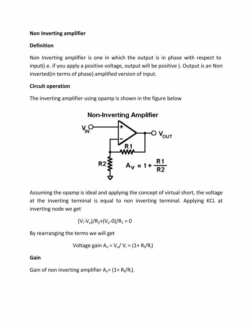
Non Inverting amplifier
Definition
Non Inverting amplifier is one in which the output is in phase with respect to
input(i.e. if you apply a positive voltage, output will be positive ). Output is an Non
inverted(in terms of phase) amplified version of input.
Circuit operation
The inverting amplifier using opamp is shown in the figure below
Assuming the opamp is ideal and applying the concept of virtual short, the voltage
at the inverting terminal is equal to non inverting terminal. Applying KCL at
inverting node we get
(Vi-Vo)/R2+(Vo-0)/R1 = 0
By rearranging the terms we will get
Voltage gain Av = Vo/ Vi = (1+ Rf/Ri)
Gain
Gain of non inverting amplifier Av= (1+ Rf/Ri).
AC CHARACTERISTICS:
For small signal sinusoidal (AC) application one has to know the ac characteristics
such as frequency response and slew-rate.
Frequency Response:
The variation in operating frequency will cause variations in gain magnitude and
its phase angle. The manner in which the gain of the op-amp responds to
different frequencies is called the frequency response. Op-amp should have an
infinite bandwidth Bw =∞ (i.e) if its open loop gain in 90dB with dc signal its gain
should remain the same 90 dB through audio and onto high radio frequency. The
op-amp gain decreases (roll-off) at higher frequency what reasons to decrease
gain after a certain frequency reached. There must be a capacitive component in
the equivalent circuit of the op-amp. For an op-amp with only one break (corner)
frequency all the capacitors effects can be represented by a single capacitor C.
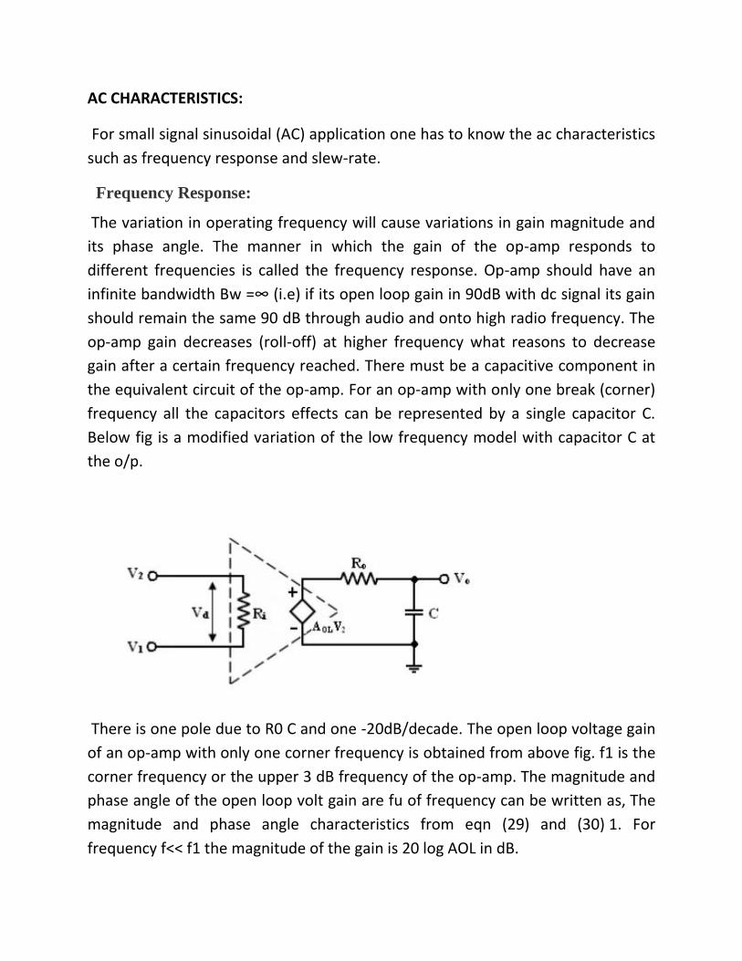
Below fig is a modified variation of the low frequency model with capacitor C at
the o/p.
There is one pole due to R0 C and one -20dB/decade. The open loop voltage gain
of an op-amp with only one corner frequency is obtained from above fig. f1 is the
corner frequency or the upper 3 dB frequency of the op-amp. The magnitude and
phase angle of the open loop volt gain are fu of frequency can be written as, The
magnitude and phase angle characteristics from eqn (29) and (30) 1. For
frequency f<< f1 the magnitude of the gain is 20 log AOL in dB.

2. At frequency f = f1 the gain in 3 dB down from the dc value of AOL in dB. This
frequency f1 is called corner frequency.
3. For f>> f1 the fain roll-off at the rate off -20dB/decade or -6dB/decade.
From the phase characteristics that the phase angle is zero at frequency f =0.
At the corner frequency f1 the phase angle is -450 (lagging and a infinite
frequency the phase angle is -900 . It shows that a maximum of 900 phase change
can occur in an op-amp with a single capacitor C. Zero frequency is taken as te
decade below the corner frequency and infinite frequency is one decade above
the corner frequency.
UNIT II
OP-AMP APPLICATIONS
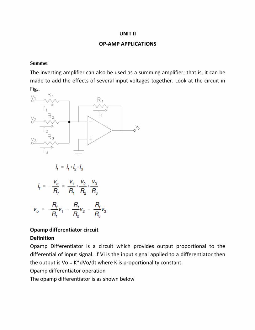
Summer
The inverting amplifier can also be used as a summing amplifier; that is, it can be
made to add the effects of several input voltages together. Look at the circuit in
Fig..
Opamp differentiator circuit
Definition
Opamp Differentiator is a circuit which provides output proportional to the
differential of input signal. If Vi is the input signal applied to a differentiator then
the output is Vo = K*dVo/dt where K is proportionality constant.
Opamp differentiator operation
The opamp differentiator is as shown below

It is obvious from the circuit shown above that negative feedback is provided
from output to inverting terminal.Using the concept of virtual ground the
inverting terminal will be at zero potential(Since the non inverting terminal of
opamp is at ground potential). the differentiator circuit can be redrawn as follows
Applying KCL at inverting node of opamp, we get
(0-Vout)/R + Ic = 0
Ic = Vout/R
where Ic = C*d(0-Vin)/dt. Hence we get Vout = -R*C*dVin/dt.
If we apply a periodic triangular signal to opamp differentiator the output will be
a periodic square wave.
Opamp integrator circuit
Integrator is a circuit which provides output proportional to the integral of input
signal.If Vi is the input signal applied to a integrator then the output is where
K is proportionality constant.
Opamp integrator operation
The opamp integrator is as shown below
It is obvious from the circuit shown above that negative feedback is provided
from output to inverting terminal.Using the concept of virtual ground the
inverting terminal will be at zero potential(Since the non inverting terminal of
opamp is at ground potential). the integrator circuit can be redrawn as follows
Applying KCL at inverting node of opamp, we get
(0-Vout)/R + Ic = 0
Ic = Vout/R
where Ic = (-1/C)* . Hence we get
Vout = – (1/R*C)*
If we apply a period square signal to opamp differentiator the output will be a
periodic triangular wave.
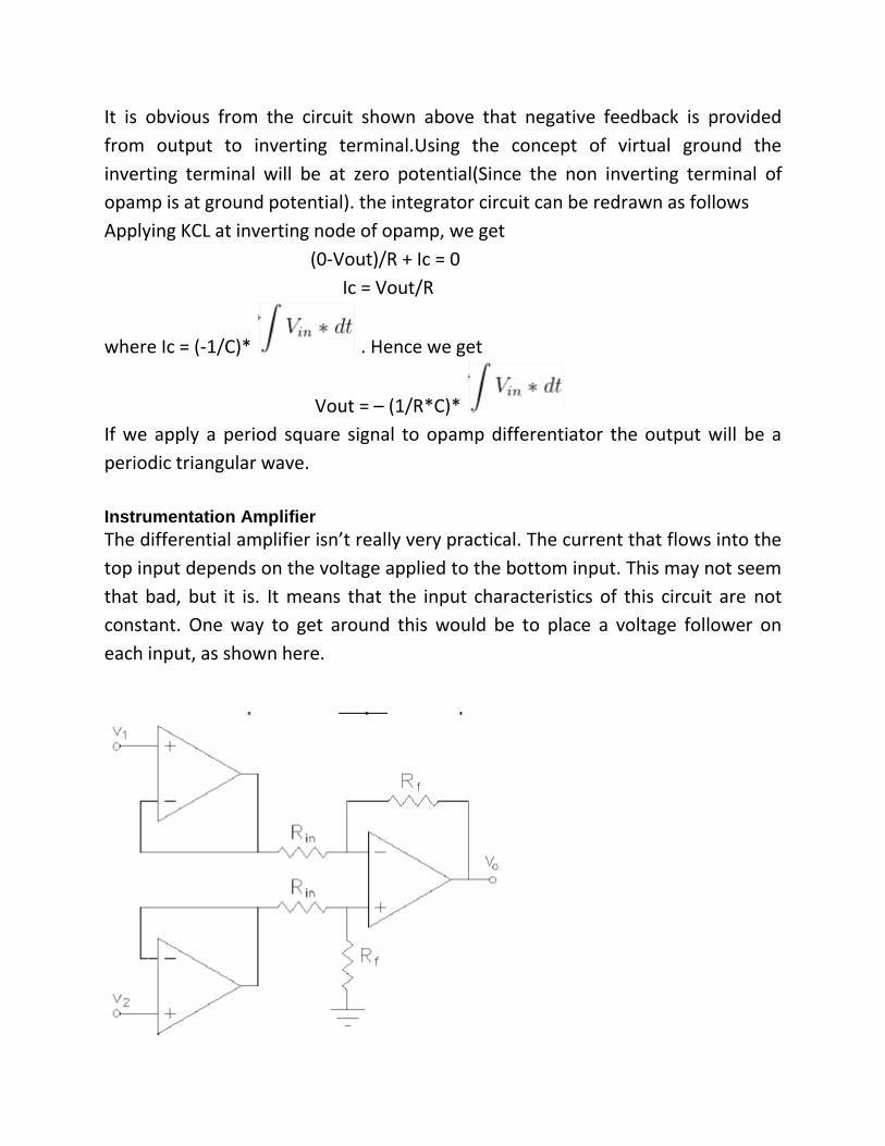
Instrumentation Amplifier
The differential amplifier isn’t really very practical. The current that flows into the
top input depends on the voltage applied to the bottom input. This may not seem
that bad, but it is. It means that the input characteristics of this circuit are not
constant. One way to get around this would be to place a voltage follower on
each input, as shown here.
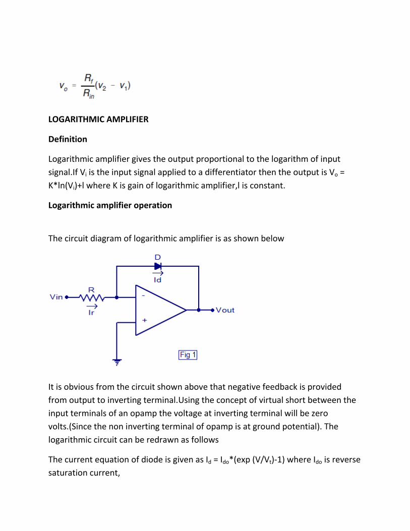
LOGARITHMIC AMPLIFIER
Definition
Logarithmic amplifier gives the output proportional to the logarithm of input
signal.If Vi is the input signal applied to a differentiator then the output is Vo =
K*ln(Vi)+l where K is gain of logarithmic amplifier,l is constant.
Logarithmic amplifier operation
The circuit diagram of logarithmic amplifier is as shown below
It is obvious from the circuit shown above that negative feedback is provided
from output to inverting terminal.Using the concept of virtual short between the
input terminals of an opamp the voltage at inverting terminal will be zero
volts.(Since the non inverting terminal of opamp is at ground potential). The
logarithmic circuit can be redrawn as follows
The current equation of diode is given as Id = Ido*(exp (V/Vt)-1) where Ido is reverse
saturation current,

V is voltage applied across diode; Vt is the voltage equivalent of temperature.
Hence applying KCL at inverting terminal of opamp, we get
(0-Vin)/R1 + Id = 0 implies Id = Vin/R1
Substituting the equation for current in the above equation we get Ido*(exp (V/Vt)-
1) = Vin/R1. Assuming exp (V/Vt) >> 1 i.e. V>>Vt and V = – Vo, we get Ido*exp (-Vo /
Vt) = Vin/R1. Applying Antilog on both sides we get
Vo = – Vt * ln (Vin/(R1*Ido)).
Gain of logarithmic amplifier
Gain of amplifier K = -Vt
ANTI LOG AMPLIFIER
Definition
Anti log amplifier is one which provides output proportional to the anti log i.e.
exponential to the input voltage.If Vi is the input signal applied to a Anti log
amplifier then the output is Vo=K*exp(a*Vi) where K is proportionality constant, a
is constant.
Anti log amplifier operation
A simple Anti log amplifier is shown below
It is obvious from the circuit shown above that negative feedback is provided
from output to inverting terminal.Using the concept of virtual short between the
input terminals of an opamp the voltage at inverting terminal will be zero
volts.(Since the non inverting terminal of opamp is at ground potential). The anti
log amplifier can be redrawn as follows
The current equation of diode is given as Id = Ido*(exp (V/Vt)-1) where Ido is reverse
saturation current,V is voltage applied across diode; Vt is the voltage equivalent of
temperature
Applying KCL at inverting node of opamp we get
Id = (0-Vo)/R = Io*(exp (Vin/Vt)) (assumed Vin /Vt >> 1)
Hence Vo = -Io*R*(exp (Vin/Vt)).
Gain of Anti log amplifier
Gain of Anti log amplifier K= -Io*R
SCHMITT TRIGGER
Definition
Schmitt trigger is an electronic circuit with positive feedback which holds the
output level till the input signal to comparator is higher than the threshold.It
converts a sinusoidal or any analog signal to digital signal. It exhibits hysteresis by
which the output transition from high to low and low to high will occur at
different thresholds.
Principle of operation
Consider a feedback system with forward gain of A and feedback factor β. If we
adjust the loop gain to be one then the gain with feedback becomes infinite. This
results in ever ending transition of output between extremes of output. Schmitt
trigger is one of such regenerative circuits also called as astable multivibrator

because of two quasi stable (unstable) states which are 1.positive extreme and
2.negative extreme.
Circuit diagram
The opamp Schmitt trigger is as shown below
It is obvious from the circuit that positive feedback is employed in the circuit. The
feedback factor
β =Vf / Vo = R2/(R2+R1).
Circuit analysis
From the figure shown above the let us assume a sinusoidal voltage is applied and
at first output is in positive saturation state. Then the feedback voltage Vf = β*Vcc.
Now when input Vin falls below β*Vcc then the voltage at inverting terminal is
greater than the voltage at non inverting terminal, so the output will be positive
and is equal to –Vcc. This value of input voltage at which output makes transition
from positive saturation voltage to negative saturation voltage is called upper
threshold.
At this point Vf = -β*Vcc now if input is allowed to fall below -β*Vcc then the
voltage at non inverting terminal is greater than the voltage at inverting terminal,
so the output makes transition from–Vcc to + Vcc. This value of input voltage at
which output makes transition from negative saturation voltage to positive
saturation voltage is called lower threshold.This process continues till sine wave
input exists at input and DC power supply for opamp is on. Below is a diagram
showing the input and output characteristics of opamp schmitt trigger
Astable Multivibrator
Definition
Astable Multivibrator is also called as Free running multivibrator or relaxation
oscillator with no stable states. It is a square wave generator and has two
unstable states.It oscillates back and forth between these two states when the
circuit is given power supply.
Circuit Diagram
Design equations
The Time period of Square wave
T = 2*R*C*ln((1+β)/(1-β))
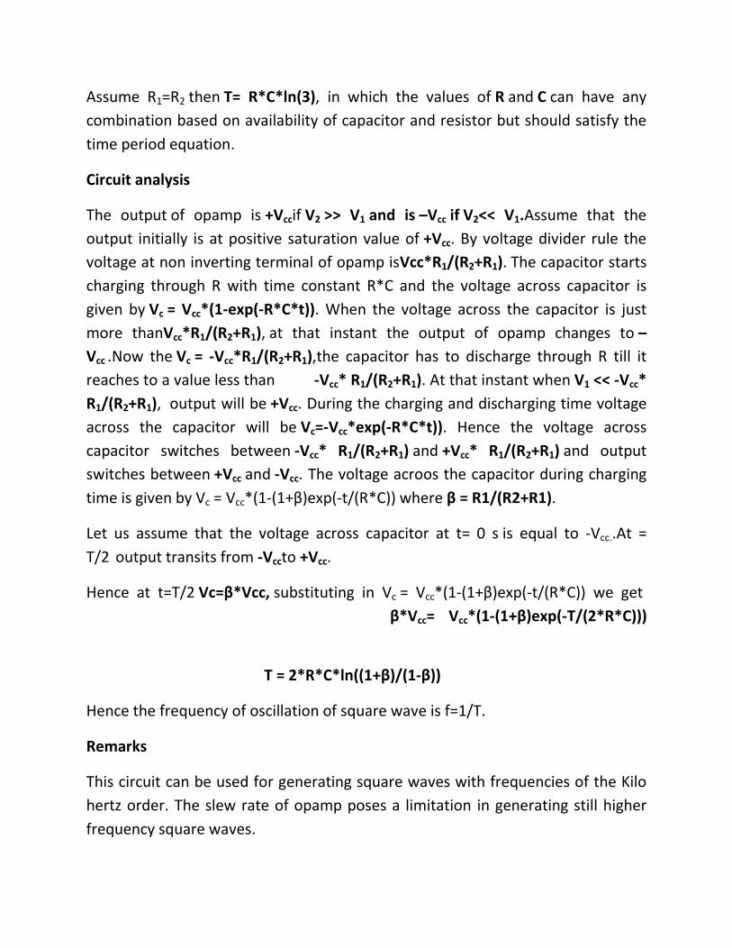
Assume R1=R2 then T= R*C*ln(3), in which the values of R and C can have any
combination based on availability of capacitor and resistor but should satisfy the
time period equation.
Circuit analysis
The output of opamp is +Vccif V2 >> V1 and is –Vcc if V2<< V1.Assume that the
output initially is at positive saturation value of +Vcc. By voltage divider rule the
voltage at non inverting terminal of opamp isVcc*R1/(R2+R1). The capacitor starts
charging through R with time constant R*C and the voltage across capacitor is
given by Vc = Vcc*(1-exp(-R*C*t)). When the voltage across the capacitor is just
more thanVcc*R1/(R2+R1), at that instant the output of opamp changes to –
Vcc .Now the Vc = -Vcc*R1/(R2+R1),the capacitor has to discharge through R till it
reaches to a value less than -Vcc* R1/(R2+R1). At that instant when V1 << -Vcc*
R1/(R2+R1), output will be +Vcc. During the charging and discharging time voltage
across the capacitor will be Vc=-Vcc*exp(-R*C*t)). Hence the voltage across
capacitor switches between -Vcc* R1/(R2+R1) and +Vcc* R1/(R2+R1) and output
switches between +Vcc and -Vcc. The voltage acroos the capacitor during charging
time is given by Vc = Vcc*(1-(1+β)exp(-t/(R*C)) where β = R1/(R2+R1).
Let us assume that the voltage across capacitor at t= 0 s is equal to -Vcc..At =
T/2 output transits from -Vccto +Vcc.
Hence at t=T/2 Vc=β*Vcc, substituting in Vc = Vcc*(1-(1+β)exp(-t/(R*C)) we get
β*Vcc= Vcc*(1-(1+β)exp(-T/(2*R*C)))
T = 2*R*C*ln((1+β)/(1-β))
Hence the frequency of oscillation of square wave is f=1/T.
Remarks
This circuit can be used for generating square waves with frequencies of the Kilo
hertz order. The slew rate of opamp poses a limitation in generating still higher
frequency square waves.
UNIT III
TIMERS & PHASE LOCKED LOOPS
INTRODUCTION
It is basically a monolithic timing circuit that produces accurate and highly stable
time delays or oscillation. When compared to the applications of an op-amp in the
same areas, the 555IC is also equally reliable and is cheap in cost. Apart from its
applications as a monostable multivibrator and astable multivibrator, a 555 timer
can also be used in dc-dc converters, digital logic probes, waveform generators,
analog frequency meters and tachometers, temperature measurement and
control devices, voltage regulators etc. The timer IC is setup to work in either of
the two modes – one-shot or monostabl or as a free-running or astable
multivibrator.The SE 555 can be used for temperature ranges between – 55°C to
125° . The NE 555 can be used for a temperature range between 0° to 70°C.
The important features of the 555 timer are :
It operates from a wide range of power supplies ranging from + 5 Volts to +
18 Volts supply voltage.
Sinking or sourcing 200 mA of load current.
The external components should be selected properly so that the timing
intervals can be made into several minutes along with the frequencies
exceeding several hundred kilo hertz.
The output of a 555 timer can drive a transistor-transistor logic (TTL) due to
its high current output.
It has a temperature stability of 50 parts per million (ppm) per degree
Celsius change in temperature, or equivalently 0.005 %/ °C.
The duty cycle of the timer is adjustable.
The maximum power dissipation per package is 600 mW and its trigger and
reset inputs has logic compatibility. More features are listed in the
datasheet.

IC Pin Configuration
Following is a brief description on the function associated with each of its
pins
Ground (Pin 1 of 8-pin and Pin 3 of 14-pin package):
Used a reference with which each of the voltage is measured.
Trigger (Pin 2 of 8-pin and Pin 4 of 14-pin package):
This pin is used to provide trigger to the circuit when the device will be
configured to behave like a monostable multivibrator. As evident from
Figure 2, it is seen that this pin is connected as an input to the comparator
C2 which compares it with 1⁄3 VCC, fed as an input to its other terminal. As
a result, when the user-provided negative pulse exceeds 1⁄3 VCC (obtained
from the resistive network), the output of this comparator goes high. This
causes the output Q of the SR flip-flop to become zero, thereby pulling its Q̅
pin high which makes the output of the inverter to go low, thereby
resulting in a high output from the IC.
Output (Pin 3 of 8-pin and Pin 5 of 14-pin package):
This is the pin at which the output of the IC can be obtained. 555 timer IC
provides two options for the user to load this pin viz., (i) Normally on load
configuration where the load is connected between the Supply and the
Output pins and (ii) Normally off load configuration where the load is
connected between the Ground and the Output pins.

Reset (Pin 4 of 8-pin and Pin 6 of 14-pin package):
This pin can be used by the user to reset the IC as the user-provided
negative going pulse on this pin switches OFF the associated transistor. This
is because, a logic low on this pin causes the output of the flip-flop to go
high, turning ON the discharge transistor. However, usually this pin will be
connected to +VCC when not in use so as to avoid false triggering.
Control Voltage (Pin 5 of 8-pin and Pin 9 of 14-pin package):
This pin is used to control the levels of threshold as well as triggering. In
addition, this pin can be used to control the pulse width of the output
waveform as the voltage applied at this pin decides the condition at which
the output of the comparator (C1) switches its state. The same regulation in
the output waveform can be even experienced by connecting
a potentiometer to this pin. Next, it is to be noted that when this pin is to
be left unused, it is to be bypassed to ground via 0.01 μF capacitor in order
to get rid of noise issue.
Threshold (Pin 6 of 8-pin and Pin 10 of 14-pin package):
This pin is connected to the positive terminal of the comparator C1 which
compares the applied voltage with 2⁄3 VCC. Next, when the user provided
voltage exceeds this reference level of 2⁄3 VCC, the output of C 1 goes high,
and thus the flip -flop's output (Q) will be set . Due to this , the complement
of its output (Q̅) will go low, resulting in a high output from the inverter,
which will be nothing but the output of the IC.
Discharge (Pin 7 of 8-pin and Pin 12 of 14-pin package):
This pin is connected to the collector terminal of the internal transistor
in 555 timer IC. Generally, a capacitor will be connected between this
terminal and ground. This capacitor discharges through the transistor when
it saturates, a phenomenon experienced when the output of comparator
C1 sets the flip-flop indicating that the threshold voltage has increased in
comparison with that of the control voltage. On the other hand, if the
negative-going trigger pulse exceeds 1⁄3 VCC, then the output of the flip-
flop goes low as the lower comparator's output will go high. This inturn

turns OFF the transistor during which the capacitor attached to its terminal
starts to charge at a rate decided by the external resistor and the capacitor.
Supply (Pin 8 of 8-pin and Pin 13 of 14-pin package): This pin is used to
provide a voltage within the range of +5V to +18V wrt ground.
555 Timer Basics The 555 timer combines a relaxation oscillator, two comparators, an R-S
flip-flop, and a discharge capacitor.
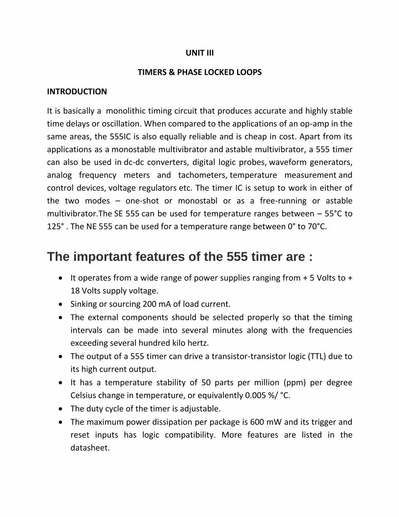
As shown in the figure, two transistors T1 and T2 are cross coupled. The
collector of transistor T1 drives the base of transistor T2 through the
resistor Rb2. The collector of transistor T2 drives the base of transistor T1
through resistor Rb1. When one of the transistor is in the saturated state,
the other transistor will be in the cut-off state. If we consider the transistor
T1 to be saturated, then the collector voltage will be almost zero. Thus
there will be a zero base drive for transistor T2 and will go into cut-off state
and its collector voltage approaches +Vcc. This voltage is applied to the
base of T1 and thus will keep it in saturation.
Now, if we consider the transistor T1 to be in the cut-off state, then the
collector voltage of T1 will be equal to +Vcc. This voltage will drive the base
of the transistor T2 to saturation. Thus, the saturated collector output of
transistor T2 will be almost zero. This value when fedback to the base of
the transistor T1 will drive it to cut-off. Thus, the saturation and cut-off
value of anyone of the transistors decides the high and low value of Q and
its compliment. By adding more components to the circuit, an R-S flip-flop
is obtained. R-S flip-flop is a circuit that can set the Q output to high or
reset it low. Incidentally, a complementary (opposite) output Q is available
from the collector of the other transistor. The schematic symbol for a S-R
flip flop is also shown above. The circuit latches in either the Q state or its
complimentary state. A high value of S input sets the value of Q to go high.
A high value of R input resets the value of Q to low. Output Q remains in a
given state until it is triggered into the opposite state.
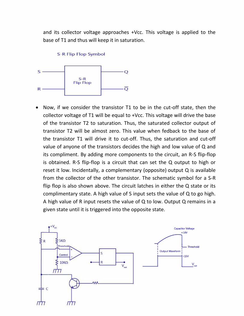
Basic Timing Concept
From the figure above, assuming the output of the S-R flip flop, Q to be
high. This high value is passed on to the base of the transistor, and the
transistor gets saturated, thus producing a zero voltage at the collector. The
capacitor voltage is clamped at ground, that is, the capacitor C is shorted
and cannot charge.
The inverting input of the comparator is fed with a control voltage, and the
non-inverting input is fed with a threshold voltage. With R-S flip flop set,
the saturated transistor holds the threshold voltage at zero. The control
voltage, however, is fixed at 2/3 VCC, that is, at 10 volts, because of the
voltage divider.
Suppose that a high voltage is applied to the R input. This resets the flip-
flop R-Output Q goes low and the transistor is cut-off. Capacitor C is now
free to charge. As this capacitor C charges, the threshold voltage rises.
Eventually, the threshold voltage becomes slightly greater than (+ 10 V).
The output of the comparator then goes high, forcing the R S flip-flop to
set. The high Q output saturates the transistor, and this quickly discharges
the capacitor. An exponential rise is across the capacitor C, and a positive
going pulse appears at the output Q. Thus capacitor voltage VC is
exponential while the output is rectangular. This is shown in the figure
above.
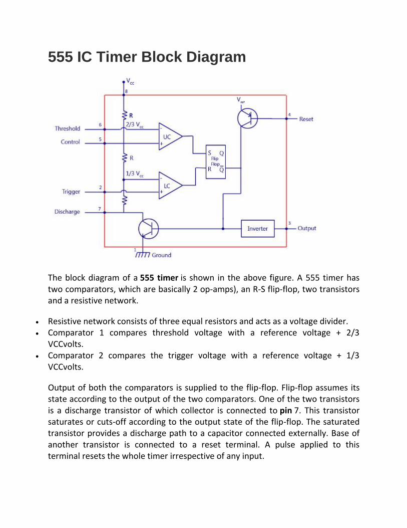
555 IC Timer Block Diagram
The block diagram of a 555 timer is shown in the above figure. A 555 timer has two comparators, which are basically 2 op-amps), an R-S flip-flop, two transistors and a resistive network.
Resistive network consists of three equal resistors and acts as a voltage divider. Comparator 1 compares threshold voltage with a reference voltage + 2/3
VCCvolts. Comparator 2 compares the trigger voltage with a reference voltage + 1/3
VCCvolts.
Output of both the comparators is supplied to the flip-flop. Flip-flop assumes its state according to the output of the two comparators. One of the two transistors is a discharge transistor of which collector is connected to pin 7. This transistor saturates or cuts-off according to the output state of the flip-flop. The saturated transistor provides a discharge path to a capacitor connected externally. Base of another transistor is connected to a reset terminal. A pulse applied to this terminal resets the whole timer irrespective of any input.

Working Principle
The internal resistors act as a voltage divider network, providing (2/3)Vcc at the non-inverting terminal of the upper comparator and (1/3)Vcc at the inverting terminal of the lower comparator. In most applications, the control input is not used, so that the control voltage equals +(2/3) VCC. Upper comparator has a threshold input (pin 6) and a control input (pin 5). Output of the upper comparator is applied to set (S) input of the flip-flop. Whenever the threshold voltage exceeds the control voltage, the upper comparator will set the flip-flop and its output is high. A high output from the flip-flop when given to the base of the discharge transistor saturates it and thus discharges the transistor that is connected externally to the discharge pin 7. The complementary signal out of the flip-flop goes to pin 3, the output. The output available at pin 3 is low. These conditions will prevail until lower comparator triggers the flip-flop. Even if the voltage at the threshold input falls below (2/3) VCC, that is upper comparator cannot cause the flip-flop to change again. It means that the upper comparator can only force the flip-flop’s output high.
To change the output of flip-flop to low, the voltage at the trigger input must fall below + (1/3) Vcc. When this occurs, lower comparator triggers the flip-flop, forcing its output low. The low output from the flip-flop turns the discharge transistor off and forces the power amplifier to output a high. These conditions will continue independent of the voltage on the trigger input. Lower comparator can only cause the flip-flop to output low.
From the above discussion it is concluded that for the having low output from the timer 555, the voltage on the threshold input must exceed the control voltage or + (2/3) VCC. This also turns the discharge transistor on. To force the output from the timer high, the voltage on the trigger input must drop below +(1/3) VCC. This turns the discharge transistor off.
A voltage may be applied to the control input to change the levels at which the switching occurs. When not in use, a 0.01 nano Farad capacitor should be connected between pin 5 and ground to prevent noise coupled onto this pin from causing false triggering.
Connecting the reset (pin 4) to a logic low will place a high on the output of flip-flop. The discharge transistor will go on and the power amplifier will output a low.
This condition will continue until reset is taken high. This allows synchronization or resetting of the circuit’s operation. When not in use, reset should be tied to +VCC.
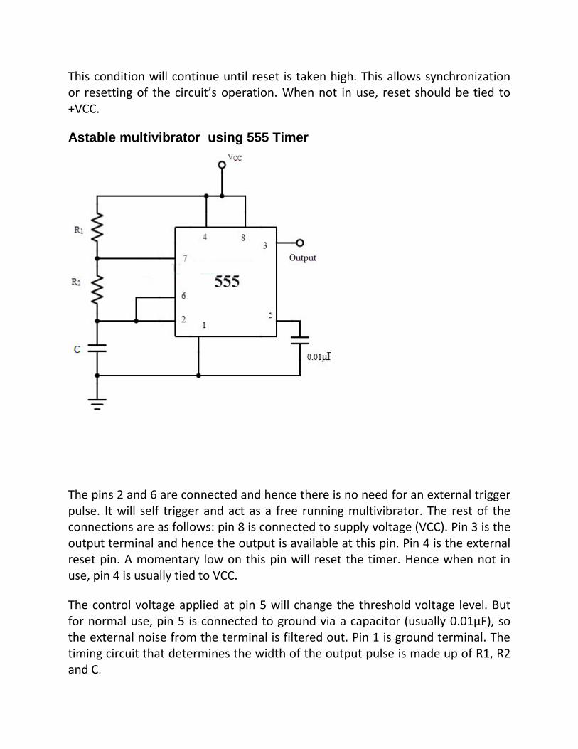
Astable multivibrator using 555 Timer
The pins 2 and 6 are connected and hence there is no need for an external trigger pulse. It will self trigger and act as a free running multivibrator. The rest of the connections are as follows: pin 8 is connected to supply voltage (VCC). Pin 3 is the output terminal and hence the output is available at this pin. Pin 4 is the external reset pin. A momentary low on this pin will reset the timer. Hence when not in use, pin 4 is usually tied to VCC.
The control voltage applied at pin 5 will change the threshold voltage level. But for normal use, pin 5 is connected to ground via a capacitor (usually 0.01µF), so the external noise from the terminal is filtered out. Pin 1 is ground terminal. The timing circuit that determines the width of the output pulse is made up of R1, R2 and C.
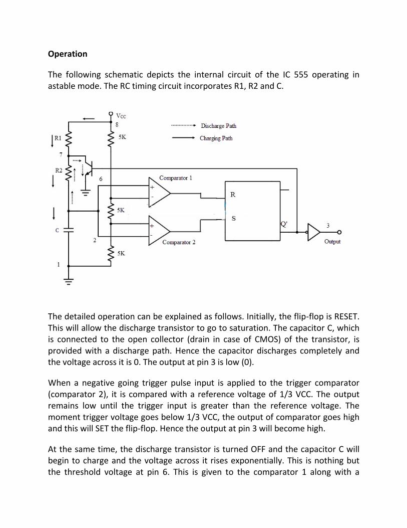
Operation
The following schematic depicts the internal circuit of the IC 555 operating in astable mode. The RC timing circuit incorporates R1, R2 and C.
The detailed operation can be explained as follows. Initially, the flip-flop is RESET. This will allow the discharge transistor to go to saturation. The capacitor C, which is connected to the open collector (drain in case of CMOS) of the transistor, is provided with a discharge path. Hence the capacitor discharges completely and the voltage across it is 0. The output at pin 3 is low (0).
When a negative going trigger pulse input is applied to the trigger comparator (comparator 2), it is compared with a reference voltage of 1/3 VCC. The output remains low until the trigger input is greater than the reference voltage. The moment trigger voltage goes below 1/3 VCC, the output of comparator goes high and this will SET the flip-flop. Hence the output at pin 3 will become high.
At the same time, the discharge transistor is turned OFF and the capacitor C will begin to charge and the voltage across it rises exponentially. This is nothing but the threshold voltage at pin 6. This is given to the comparator 1 along with a
reference voltage of 2/3 VCC. The output at pin 3 will remain HIGH until the voltage across the capacitor reaches 2/3 VCC.
The instance at which the threshold voltage (which is nothing but the voltage across the capacitor) becomes more than the reference voltage, the output of the comparator 1 goes high. This will RESET the flip-flop and hence the output at pin 3 will fall to low (logic 0) i.e. the output returns to its stable state. As the output is low, the discharge transistor is driven to saturation and the capacitor will completely discharge.
Hence it can be noted that the output at pin 3 is low at start, when the trigger becomes less than 1/3 VCC the output at pin 3 goes high and when the threshold voltage is greater than 2/3 VCC the output becomes low until the occurrence of next trigger pulse. A rectangular pulse is produced at the output. The time for which the output stays high or the width of the rectangular pulse is controlled by the timing circuit i.e. the charging time of the capacitor which depends on the time constant RC.
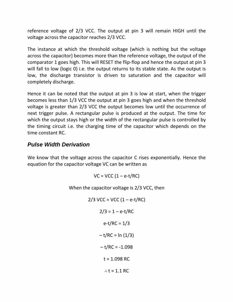
Pulse Width Derivation
We know that the voltage across the capacitor C rises exponentially. Hence the equation for the capacitor voltage VC can be written as
VC = VCC (1 – e-t/RC)
When the capacitor voltage is 2/3 VCC, then
2/3 VCC = VCC (1 – e-t/RC)
2/3 = 1 – e-t/RC
e-t/RC = 1/3
– t/RC = ln (1/3)
– t/RC = -1.098
t = 1.098 RC
∴ t ≈ 1.1 RC
The pulse width of the output rectangular pulse is W = 1.1 RC.
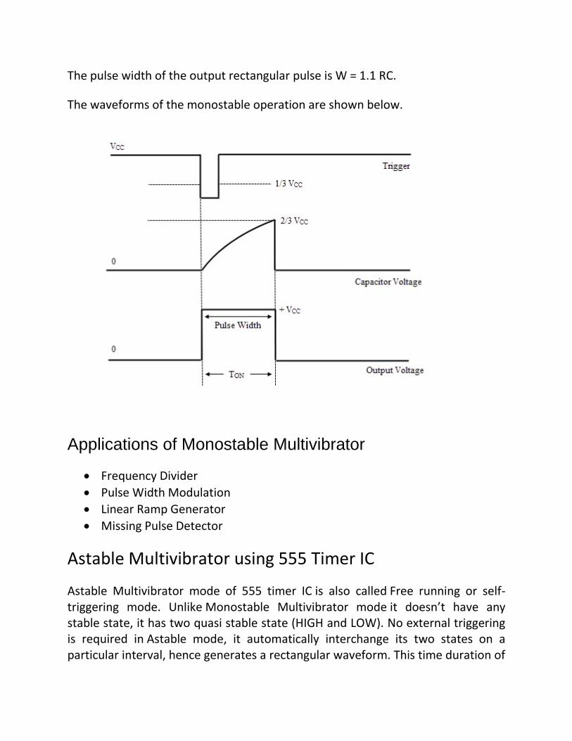
The waveforms of the monostable operation are shown below.
Applications of Monostable Multivibrator
Frequency Divider
Pulse Width Modulation
Linear Ramp Generator
Missing Pulse Detector
Astable Multivibrator using 555 Timer IC
Astable Multivibrator mode of 555 timer IC is also called Free running or self-triggering mode. Unlike Monostable Multivibrator mode it doesn’t have any stable state, it has two quasi stable state (HIGH and LOW). No external triggering is required in Astable mode, it automatically interchange its two states on a particular interval, hence generates a rectangular waveform. This time duration of
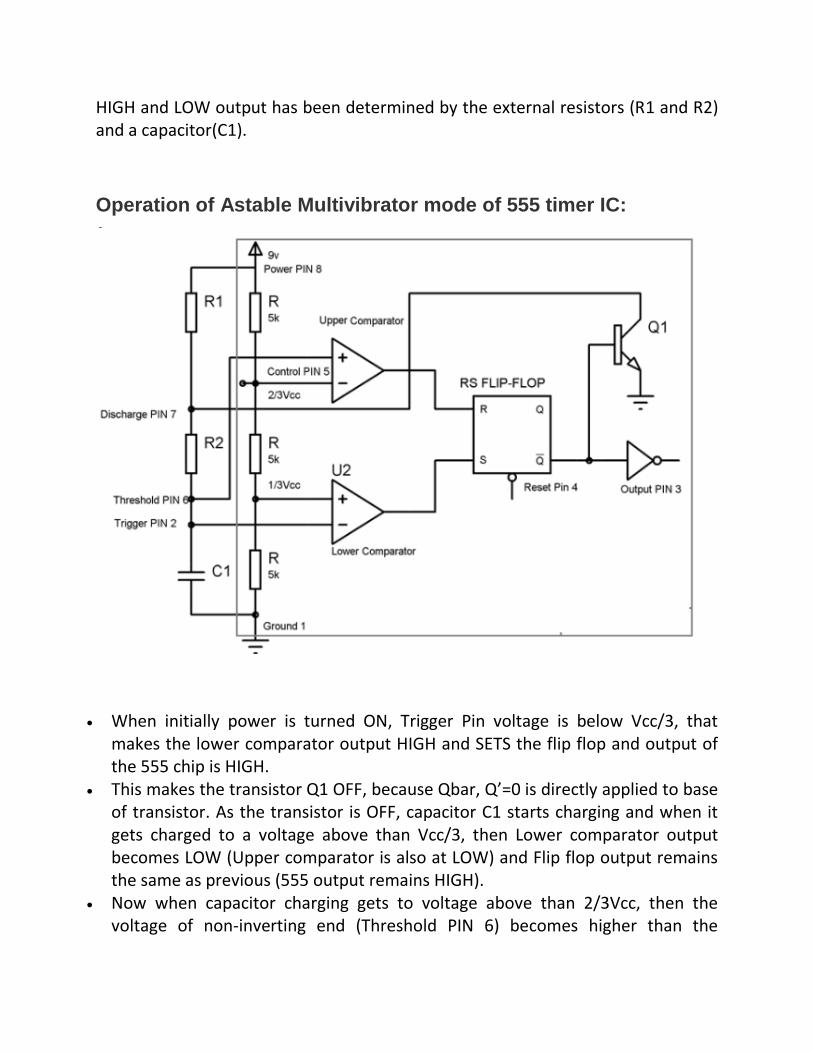
HIGH and LOW output has been determined by the external resistors (R1 and R2) and a capacitor(C1).
Operation of Astable Multivibrator mode of 555 timer IC:
When initially power is turned ON, Trigger Pin voltage is below Vcc/3, that makes the lower comparator output HIGH and SETS the flip flop and output of the 555 chip is HIGH.
This makes the transistor Q1 OFF, because Qbar, Q’=0 is directly applied to base of transistor. As the transistor is OFF, capacitor C1 starts charging and when it gets charged to a voltage above than Vcc/3, then Lower comparator output becomes LOW (Upper comparator is also at LOW) and Flip flop output remains the same as previous (555 output remains HIGH).
Now when capacitor charging gets to voltage above than 2/3Vcc, then the voltage of non-inverting end (Threshold PIN 6) becomes higher than the
inverting end of the comparator. This makes Upper comparator output HIGH and RESETs the Flip flop, output of 555 chip becomes LOW.
As soon as the output of 555 get LOW means Q’=1, then transistor Q1 becomes ON and short the capacitor C1 to the Ground. So the capacitor C1 starts discharging to the ground through the Discharge PIN 7 and resistor R2.
As capacitor voltage get down below the 2/3 Vcc, upper comparator output becomes LOW, now SR Flip flop remains in the previous state as both the comparators are LOW.
While discharging, when capacitor voltage gets down below Vcc/3, this makes the Lower comparator output HIGH (upper comparator remain LOW) and Sets the flip flop again and 555 output becomes HIGH.
Transistor Q1 becomes OFF and again capacitor C1 starts charging.
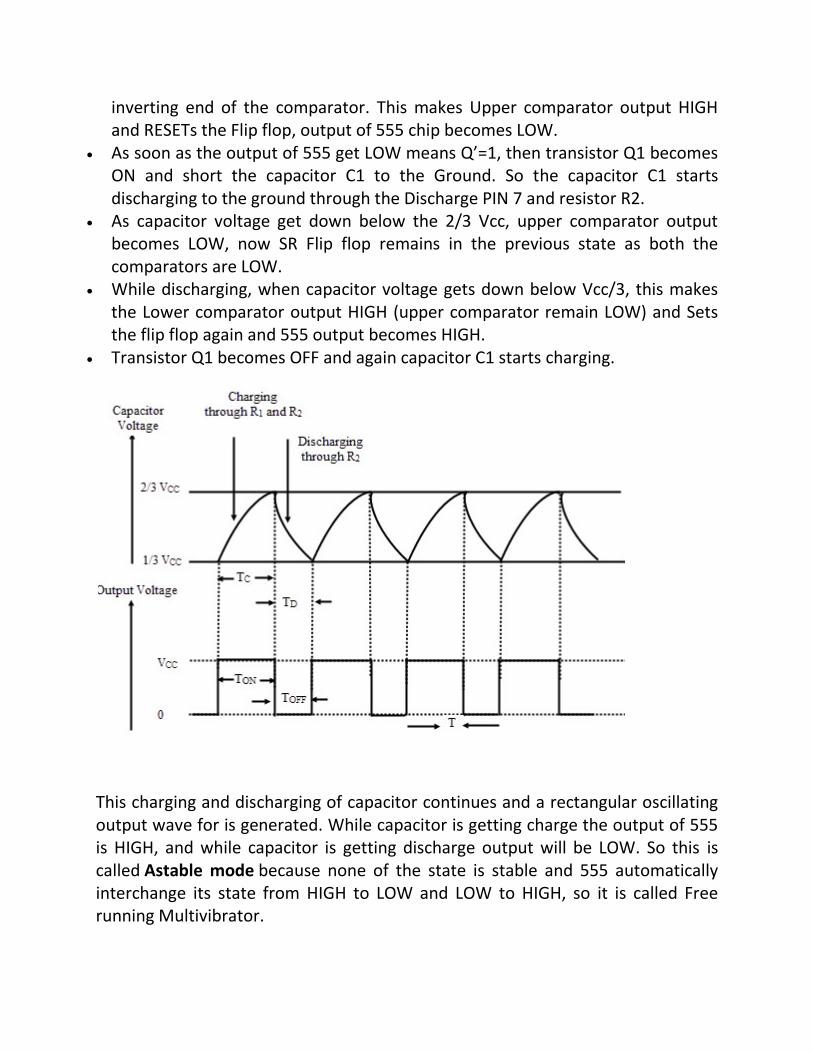
This charging and discharging of capacitor continues and a rectangular oscillating output wave for is generated. While capacitor is getting charge the output of 555 is HIGH, and while capacitor is getting discharge output will be LOW. So this is called Astable mode because none of the state is stable and 555 automatically interchange its state from HIGH to LOW and LOW to HIGH, so it is called Free running Multivibrator.
Now the OUTPUT HIGH and OUTPUT LOW duration, is determined by the Resistors R1 & R2 and capacitor C1. This can be calculated using below formulas:
Time High (Seconds) T1 = 0.693 * (R1+R2) * C1
Time Low (Seconds) T2 = 0.693 * R2 * C1
Time Period T = Time High + Time Low = 0.693 * (R1+2*R2) * C1
Freqeuncy f = 1/Time Period = 1/ 0.693 * (R1+2*R2) * C1 = 1.44 / (R1+2*R2) * C1
Duty Cycle: Duty cycle is the ratio of time for which the output is HIGH to the total time.
Duty cycle %: (Time HIGH/ Total time) * 100 = (T1/T) * 100 = (R1+R2)/ (R1+2*R2) *100
Here is the practical demonstration of the Astable mode of 555 timer IC, where we have connected a LED to the output of the 555 IC. In this 555 astable multivibrator circuit, LED will switch ON and OFF automatically with a particular duration. ON time, OFF time, Frequency etc can be calculated using above formulas.
PHASE LOCKED LOOP
A phase locked loop consist of a phase detector and a voice control oscillator. The output of the phase detector is the input of the voice control oscillator (VCO) and the output of the VCO is connected to one of the inputs of phase detector which is shown below in the basic block diagram. When these two devices are feed to each other the loop forms.

Block Diagram And Working Principle Of PLL
The phase locked loop consists of a phase detector, a voltage control oscillator and, in between them, a low pass filter is fixed. The input signal ‘Vi’ with an input frequency ‘Fi’ is conceded by a phase detector. Basically the phase detector is a comparator which compares the input frequency fi through the feedback frequency fo. The output of the phase detector is (fi+fo) which is a DC voltage. The out of the phase detector, i.e., DC voltage is input to the low pass filter (LPF); it removes the high frequency noise and produces a steady DC level, i.e., Fi-Fo. The Vf is also a dynamic characteristic of the PLL.
The output of the low pass filter, i.e., DC level is passed on to the VCO. The input signal is directly proportional to the output frequency of the VCO (fo). The input and output frequencies are compared and adjusted through the feedback loop until the output frequency is equal to the input frequency. Hence, the PLL works like free running, capture, and phase lock.
When there is no input voltage applied, then it is said to be as a free running stage. As soon as the input frequency applied to the VOC changes and produces an output frequency for comparison, it is called as capture stage. The below figure
shows the block diagram of the PLL.

Phase Locked Loop Detector
The phase locked loop detector compares the input frequency and the output frequency of the VCO to produces a DC voltage which is directly proportional to the phase distinction of the two frequencies. The analog and digital signals are used in the phase locked loop. Most of the monolithic PLL integrated circuits uses an analog phase detector and majority of phase detectors are from the digital type. A double balanced mixture circuit is used commonly in analog phase detectors. Some common phase detectors are given below:
Exclusive OR Phase Detector
An exclusive OR phase detector is CMOS IC 4070 type. The input and output frequencies are applied to the EX OR phase detector. To obtain the output high at least one input should be low and the other conditions of output are low which is shown in the below truth table. Let us consider the waveform, the input and output frequencies, i.e. fi and fo have a phase difference of 0 degrees. Then the DC output voltage of the comparator will be a function of the phase difference between the two inputs.
PLL Applications
Frequency Modulation (FM) stereo decoders, FM Demodulation networks for FM operation.
Frequency synthesis that provides multiple of a reference signal frequency.
Used in motorspeed controls, tracking filters.
Used in frequency shift keying (FSK) decodes for demodulation carrier frequencies.
UNIT IV
D-A AND A- D CONVERTERS
Digital to Analog Converters (D/A)
A D/A Converter is used when the binary output from a digital system is to be converted into its equivalent analog voltage or current.
The binary output will be a sequence of 1’s and 0’s. Thus they ma be difficult to follow. But, a D/A converter help the user to interpret easily.
Basically, a D/A converter have an op-amp. It can be classified into 2 types. They are
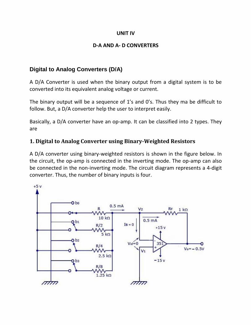
1. Digital to Analog Converter using Binary-Weighted Resistors
A D/A converter using binary-weighted resistors is shown in the figure below. In the circuit, the op-amp is connected in the inverting mode. The op-amp can also be connected in the non-inverting mode. The circuit diagram represents a 4-digit converter. Thus, the number of binary inputs is four.
We know that, a 4-bit converter will have 24 = 16 combinations of output. Thus, a corresponding 16 outputs of analog will also be present for the binary inputs.
Four switches from b0 to b3 are available to simulate the binary inputs: in practice, a 4-bit binary counter such as a 7493 can also be used.
Working
The circuit is basically working as a current to voltage converter.
b0 is closed
It will be connected directly to the +5V.
Thus, voltage across R = 5V
Current through R = 5V/10kohm = 0.5mA
Current through feedback resistor, Rf = 0.5mA (Since, Input bias current, IB is negligible)
Thus, output voltage = -(1kohm)*(0.5mA) = -0.5V
b1 is closed, b0 is open
R/2 will be connected to the positive supply of the +5V.
Current through R will become twice the value of current (1mA) to flow through Rf.
Thus, output voltage also doubles.
b0 and b1 are closed
Current through Rf = 1.5mA
Output voltage = -(1kohm)*(1.5mA) = -1.5V
Thus, according to the position (ON/OFF) of the switches (bo-b3), the corresponding “binary-weighted” currents will be obtained in the input resistor.
The current through Rf will be the sum of these currents. This overall current is then converted to its proportional output voltage. Naturally, the output will be maximum if the switches (b0-b3) are closed
V0 = -Rf *([b0/R][b1/(R/2)][b2/(R/4)][b3/(R/8)]) – where each of the inputs b3, b2, b1, and b0 may either be HIGH (+5V) or LOW (0V).
The graph with the analog outputs versus possible combinations of inputs is shown below.
The output is a negative going staircase waveform with 15 steps of -).5V each. In practice, due to the variations in the logic HIGH voltage levels, all the steps will not have the same size. The value of the feedback resistor Rf changes the size of the steps. Thus, a desired size for a step can be obtained by connecting the appropriate feedback resistor. The only condition to look out for is that the maximum output voltage should not exceed the saturation levels of the op-amp. Metal-film resistors are more preferred for obtaining accurate outputs.
Disadvantages
If the number of inputs (>4) or combinations (>16) is more, the binary-weighted resistors may not be readily available. This is why; R and 2R method is more preferred as it requires only two sets of precision resistance values.
2. Digital to Analog Converter with R and 2R Resistors
A D/A converter with R and 2R resistors is shown in the figure below. As in the binary-weighted resistors method, the binary inputs are simulated by the switches (b0-b3), and the output is proportional to the binary inputs. Binary inputs can be either in the HIGH (+5V) or LOW (0V) state. Let b3 be the most significant bit and thus is connected to the +5V and all the other switchs are connected to the ground.
Thus, according to Thevenin’s equivalent resistance, RTH,
RTH = [{[(2RII2R + R)} II2R] + R}II2R] + R = 2R = 20kOhms.
The resultant circuit is shown below.
Graph is given below.
In the figure shown above, the negative input is at virtual ground, therefore the current through RTH=0.
Current through 2R connected to +5V = 5V/20kohm = 0.25 mA
The current will be the same as that in Rf.
Vo = -(20kohm)*(0.25mA) = -5V
Output voltage equation is given below.
V0 = -Rf (b3/2R+b2/4R+b1/8R+b0/16R)
ANALOG-DIGITAL CONVERTER
An Analog-Digital Converter (ADC) is a widely used electronic component that converts an analog electric signal (usually a voltage) into a digital representation. The ADCs are at the front-end of any digital circuit that needs to process signals coming from the exterior world. Its schematic symbol is:
The output of a microphone, the voltage at a photodiode or the signal of an accelerometer are examples of analog values that need to be converted so that a microprocessor can work with them.
Many ways have been developed to convert an analog signal, each with its strengths and weaknesses. The choice of the ADC for a given application is usually defined by the requirements you have: if you need speed, use a fast ADC; if you need precision, use an accurate ADC; if you are constrained in space, use a compact ADC.
All ADCs work under the same principle: they need to convert a signal to a certain number of bits N. The sequence of bits represents the number and each bit has the double of the weight of the next, starting from the Most Significant Bit (MSB) up to the Least Significant Bit (LSB). In a nutshell, we want to find the sequence of bits bN−1, bN−2, ..., b0 that represents the analog value Vin as
Flash Converters
A simple way to get better (more bits of) resolution is to use more comparators. As shown below for a 2-bit flash converter we can use 2N 1 comparators, supplying them with reference voltages that are equally spaced over the desired conversion range. The other comparator inputs are connected to the input signal.
All of the digital outputs connected to reference voltages below the input signal will be true and all of the outputs with reference signals above the input signal level will be false. The output logic circuit converts these 2N 1 binary values into an N-bit number.
Successive Approximation Converters
Another approach is to use a D/A converter to generate the reference voltage and a single comparator to compare this voltage and the input. A digital circuit can step the D/A output up through the possible values until the comparator indicates that the reference signal is greater than the input signal. The digital input to the D/A would correspond to the voltage step that is the next-highest to the input signal. This approach would take up to 2N comparisons.
A faster method is to use a binary search. The control circuit first tests whether the analog input is greater than or less than half of the D/A output range. This fixes the value of the most significant bit. Then the controller tests whether the value is greater than or less than the half-way point of the remaining range. This sets the next most-significant bit. The process is repeated until the values of all of the bits are determined. The time required for this method is about N times the D/A settling time. This method is slower than a flash converter but reduces the number of comparators required. Successive approximation converters are probably the most common type of general-purpose ADCs.
Sample and Hold
If the analog signal changes while a conversion is taking place, the ADC could produce an incorrect result. A device called a sample-and-hold can be used before the ADC to hold the signal at the input to the ADC constant. This device samples the analog signal at its input for a short time and then holds that value fixed at its output until the next sample is required. The diagram below shows how the device works. An electronic switch is used to connect the analog input to a capacitor during the sampling time. During the “hold” time the switch is opened. An output amplifier with a very high input impedance is used in order to avoid discharging the capacitor during the hold time
UNIT V
SPECIAL FUNCTION ICS
INTRODUCTION
A voltage regulator is used to regulate voltage level. When a steady, reliable voltage is needed, then voltage regulator is the preferred device. It generates a fixed output voltage that remains constant for any changes in an input voltage or load conditions. It acts as a buffer for protecting components from damages. A voltage regulator is a device with a simple feed- forward design and it uses negative feedback control loops. There are mainly two types of voltage regulators: Linear voltage regulators and switching voltage regulators; these are used in wider applications. Linear voltage regulator is the easiest type of voltage regulators. It is available in two types, which are compact and used in low power, low voltage systems. Let us discuss about different types of voltage regulators.
Types of Voltage Regulators and Their Working Principle
Basically, there are two types of Voltage regulators: Linear voltage regulator and Switching voltage regulator.
There are two types of Linear voltage regulators: Series and Shunt.
There are three types of Switching voltage regulators: Step up, Step down and Inverter voltage regulators.
Linear Regulator
Linear regulator acts like a voltage divider. In Ohmic region, it uses FET. The resistance of the voltage regulator varies with load resulting in constant output voltage.
Advantages of linear voltage regulator
Gives a low output ripple voltage
Fast response time to load or line changes
Low electromagnetic interference and less noise

Disadvantages of linear voltage regulator
Efficiency is very low
Requires large space – heatsink is needed
Voltage above the input cannot be increased
Series Voltage Regulator
A series voltage regulator uses a variable element placed in series with the load.
By changing the resistance of that series element, the voltage dropped across it
can be changed. And, the voltage across the load remains constant.
The amount of current drawn is effectively used by the load; this is the main
advantage of the series voltage regulator. Even when the load does not require
any current, the series regulator does not draw full current. Therefore, a series
regulator is considerably more efficient than shunt voltage regulator.
Shunt Voltage Regulator
A shunt voltage regulator works by providing a path from the supply voltage to ground
through a variable resistance. The current through the shunt regulator is diverted
away from the load and flows uselessly to the ground, making this form usually
less efficient than the series regulator. It is, however, simpler, sometimes
consisting of just a voltage-reference diode, and is used in very low-powered
circuits wherein the wasted current is too small to be of concern. This form is very
common for voltage reference circuits. A shunt regulator can usually only sink
(absorb) current.
Applications of Shunt Regulators
Shunt regulators are used in:
Low Output Voltage Switching Power Supplies
Current Source and Sink Circuits
Error Amplifiers
Adjustable Voltage or Current Linear and Switching Power Supplies
Voltage Monitoring
Analog and Digital Circuits that require precision references
Precision current limiters

Switching Voltage Regulator
A switching regulator rapidly switches a series device on and off. The switch’s
duty cycle sets the amount of charge transferred to the load. This is controlled by
a feedback mechanism similar to that of a linear regulator. Switching regulators
are efficient because the series element is either fully conducting or switched off
because it dissipates almost no power. Switching regulators are able to generate
output voltages that are higher than the input voltage or of opposite polarity,
unlike linear regulators.
POWER AUDIO AMPLIFIER IC LM380:
Features of LM380:
1. Internally fixed gain of 50 (34dB) 2. Output is automatically self centring to one half of the supply voltage. 3. Output is short circuit proof with internal thermal limiting. 4. Input stage allows the input to be ground referenced or ac coupled. 5. Wide supply voltage range (5 to 22V). 6. High peak current capability. 7. High impedence. 8. Low total harmonic distortion
9. Bandwidth of 100KHz at Pout = 2W & RL = 8Ω

Introduction:
Small signal amplifier are essentially voltage amplifier that supply their loads with
larger amplifier signal voltage. On the other hand , large signal or power amplifier
supply a large signal current to current operated loads such as speakers & motors.
In audio applications, however, the amplifier called upon to deliver much higher
current than that suppkied by general purpose op-amps. This means that loads
such as speakers & motors requiring substantial currents cannot be driven directly
by the output of general purpose opo-amps.
However there are two possible solutions,
To use discrete or monolithic power transistors called power boosters at the
output of the op-amp
To use specialized ICs designed as power amplifiers.

LM380 circuit description:
It is connected of 4 stages,
(i) PNP emitter follower
(ii) Different amplifier
(iii) Common emitter
(iv) Emitter follower
(i) PNP Emitter follower:
· The input stage is emitter follower composed of PNP transistors Q1 &
Q2 which drives the PNP Q3-Q4 differential pair.
· The choice of PNP input transistors Q1 & Q2 allows the input to be
referenced to ground i.e., the input can be direct coupled to either the inverting &
non-inverting terminals of the amplifier.
(ii) Differential Amplifier:
· The current in the PNP differential pair Q3-Q4 is established by Q7, R3 &
+V.
· The current mirror formed by transistor Q7, Q8 & associated resistors then
establishes the collector current of Q9.
· Transistor Q5 & Q6 constitute of collector loads for the PNP differential
pair.
· The output of the differential amplifier is taken at the junction of Q4 &
Q6 transistors & is applied as an input to the common emitter voltage gain.
(iii) Common Emitter:
· Common Emitter amplifier stage is formed by transistor Q9 with D1, D2 &
Q8 as a current source load.
· The capacitor C between the base & collector of Q9 provides internal
compensation & helps to establish the upper cutoff frequency of 100 KHz.
· Since Q7 & Q8 form a current mirror, the current through D1 & D2 is
approximately the same as the current through R3.
· D1 & D2 are temperature compensating diodes for transistors Q10 &
Q11 in that D1 & D2 have the same characteristics as the base-emitter junctions
of Q11. Therefore the current through Q10 & (Q11-Q12) is approximately equal to
the current through diodes D1 & D2.
(iv)(Output stage) - Emitter follower:
· Emitter follower formed by NPN transistor Q10 & Q11. The combination of PNP
transistor Q11 & NPN transistor Q12 has the power capability of an NPN transistors but the
characteristics of a PNP transistor.
· The negative dc feedback applied through R5 balances the differential amplifier so that
the dc output voltage is stabilized at +V/2;
· To decouple the input stage from the supply voltage +V, by pass capacitor in order of
micro farad should be connected between the by pass terminal (pin 1) & ground (pin 7).
· The overall internal gain of the amplifier is fixed at 50. However gain can be increased
by using positive feedback.
APPLICATIONS:
i. Audio Power Amplifier:
Amplifier requires very few external components because of the internal
biasing, compensation & fixed gain.
When the power amplifier is used in the non inverting configuration, the
inverting terminal may be either shorted to ground, connected to ground through
resistors & capacitors.
Similarly when the power amplifier is used in the inverting mode, the non
inverting terminal may be either shorted to ground or returned to ground through
resistor or capacitor.
Usually a capacitor is connected between the inverting terminal & ground if
the input has a high internal impedance.
As a precautionary measure, an RC combination should be used at the output
terminal (pin 8) to eliminate 5-to-10 MHz oscillation.
C1 is coupling capacitor which couples the output of the amplifier to the 8
ohms loud speaker which act as a load. The amplifier will amplify the Vin applied
at the non-inverting terminal.
(ii) LM 380 as a High gain:
The gain of LM380 is internally fixed at 50. But it can be increased by using the
external components.
The increase in gain is possible due to the use of positive feedback, this setup
to obtain a gain 200.
(iii) LM 380 as a variable Gain:
Instead of getting a fixed gain of 50, it is possible to obtain a variable gain up
to 50 by connecting a potentiometer between the input terminals.
Optocoupler IC:
The optocouplers are available in the IC form MCT2E is the standard optocoupler
IC which is used popularly in many electronic application.
· This input is applied between pin 1& pin 2. An infrared light emitting
diode is connected between these pins.
· The infrared radiation from the LED gets focused on the internal
phototransistor.
· The base of the phototransistor is generally left open. But sometimes a
high value pull down resistance is connected from the Base to ground to improve
the sensitivity.
· The block diagram shows the opto-electronic-integrated ciruit (OEIC) and
the major components of a fiber-optic communication facility.
