behavioral simulation of a second order discrete time...
TRANSCRIPT

1
BehavioralSimulationofASecondOrderDiscreteTimeDelta‐SigmaADCUsingCppSim
WalaSaadehAymanShabraMichaelPerrot
MasdarInstituteofScienceandTechnology,UAE
December7,2013
Copyright © 2013 by Wala Saadeh All rights reserved.
Table of Contents Setup...............................................................................................................................................................2 Introduction...............................................................................................................................................4 A.Delta‐SigmaModulators............................................................................................................4 B.DeltaSigmaMatlabToolbox...................................................................................................5 C.SecondOrderDeltaSigmaADCExample.........................................................................6
Preliminaries..........................................................................................................................................14 A.OpeningSue2Schematics......................................................................................................14 B.RunningCppSimSimulations..............................................................................................15
PlottingTime‐DomainResults......................................................................................................17 A.OutputSignalPlots....................................................................................................................18 B.MatlabVerificationofOutputSpectrum.......................................................................22
Conclusion................................................................................................................................................25 References................................................................................................................................................25 AppendixA:MatlabSynthesisCode...........................................................................................26 AppendixB:MatlabVerificationCode(calculate_snr.m)..............................................29

2
Setup Download and install the CppSim Version 5 package (i.e., download and run theself‐extractingfilenamedsetup_cppsim5.exe)locatedat:
http://www.cppsim.com/download.htmlUpon completion of the installation, you will see icons on the Windows desktopcorrespondingtotheSue2,CppSimView,andPLLDesignAssistant.Pleasereadthe“CppSim/VppSimPrimer” document, which is also at the sameweb address, tobecomeacquaintedwithCppSimanditsvariouscomponents.Youshouldalsoreadthe manual “PLL Design Using the PLL Design Assistant Program”, which islocated at http://www.cppsim.com, to obtain more information about the PLLDesignAssistantasitisbrieflyusedinthisdocument.To run this tutorial, you will also need to download the filesigma_delta_ord2_dt_adc_example.tar.gz available at http://www.cppsim.com,and place it in the Import_Export directory of CppSim (assumed to bec:/CppSim/Import_Export).Onceyoudoso,startupSue2byclickingonitsicon,andthenclickonTools‐>LibraryManagerasshowninthefigurebelow.
IntheCppSimLibraryManagerwindowthatappears,clickontheImportLibraryToolbuttonasshowninthefigurebelow.
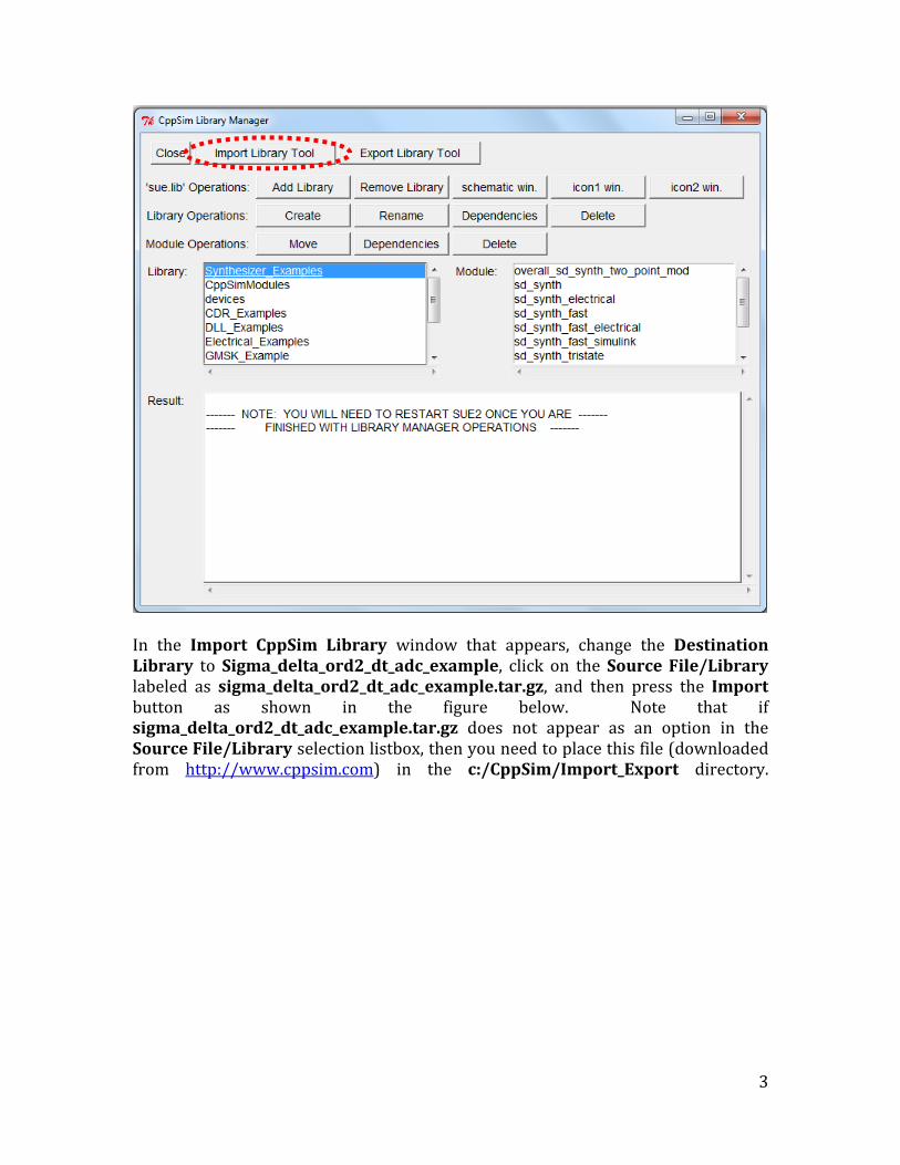
3
In the Import CppSim Library window that appears, change the DestinationLibrary to Sigma_delta_ord2_dt_adc_example, click on the SourceFile/Librarylabeled as sigma_delta_ord2_dt_adc_example.tar.gz, and then press the Importbutton as shown in the figure below. Note that ifsigma_delta_ord2_dt_adc_example.tar.gz does not appear as an option in theSourceFile/Libraryselectionlistbox,thenyouneedtoplacethisfile(downloadedfrom http://www.cppsim.com) in the c:/CppSim/Import_Export directory.

4
Once you have completed the above steps, restart Sue2 as directed in the abovefigure.Introduction CppSim is a free behavioral simulation package that leverages the C++ language to allow very fast simulation of a wide array of system types. The goal of this tutorial is to expose the reader to a Sigma-Delta ADC system where modeling with CppSim enables the exploration of key design issues, and may inspire new architectures for improved performance. A.Delta‐SigmaModulatorsDelta-Sigma () modulators have been in existence for many years and have found adoption in a huge number of circuits and systems applications, from instrumentation to communications. The key advantage of these converters is that they provide a low cost and robust implementation for achieving wide dynamic range and high resolution in converting low bandwidth input signals. The combination of oversampling and quantization noise shaping techniques allow

5
modulators to be immune to many analog circuit limitations, thus making them extensively used to realize embedded analog-to-digital interfaces in modern systems-on-chip (SoCs) integrated in advanced CMOS processes1. Over the last few years, significant efforts have been made to decrease the power consumption and to increase the speed of , while at the same time maintaining flexibility and compatibility with mainstream digital technologies. The conceptual block diagram of basic 1st order ADC is shown in Figure 1 and is built around summers, integrators, quantizers, DACs, and digital decimation filters.
Figure 1: First Order ADC block diagram
Adeltasigmamodulatorhasthreedegreesoffreedomtooptimizeitsperformance,whicharemodulator‐order,quantizerresolutionandtheoversamplingratio(OSR).Thedegreetowhichthequantizationnoisecanbeattenuateddependsontheorderofthenoiseshapingandtheoversamplingratio.Giventhe inputsignalbandwidth(BW),andafterchoosingareasonableclockfrequencyfs,wecalculateOSR=
∗.
Each octave increase inOSR increasesMOD1 (order = 1) SNR by 9dB andMOD2(order=2)SNRby15dB[1][2].B.DeltaSigmaMatlabToolboxRichard Schreier’s Delta-Sigma Matlab Toolbox is a state of the art tool for the design, simulation and realization of ADCs. The toolbox is widely utilized in generating the required coefficients for topologies based on the input target specifications. The Delta-Sigma Toolbox includes many functions which support NTF synthesis, modulator simulation, realization, dynamic range scaling, SNR estimation and much more. The toolbox can be downloaded from the MathWorks file exchange website: http://www.mathworks.com/matlabcentral/fileexchange/19‐delta‐sigma‐toolbox/all_filesThe toolbox documentation is the file DSToolbox.pdf which is available as part of the download from the MathWorks file exchange website above.
1delaRosa,J.M.;,"Sigma‐DeltaModulators:TutorialOverview,DesignGuide,andState‐of‐the‐ArtSurvey,"CircuitsandSystemsI:RegularPapers,IEEETransactionson,vol.58,no.1,pp.1‐21,Jan.2011
Q
CLK
VU
Y
DAC
Digital Filter
Dout

6
C.SecondOrderDeltaSigmaADCExampleTo develop a basic understanding of the design flow of a ADC, an overview example is provided here. The design process will start with specifications such as input bandwidth and SNR. The delsig toolbox will be used to synthesize a transfer function and then realize it as a blocked diagram. The block diagram can be mapped to a circuit implementation and CppSim allows fast behavioral simulations using analog components such as opamps, switches, and comparators. The behavioral simulation will aid in validating the circuit topology and verifying that it meets the target specifications. A very useful aspect of the CppSim capabilities is its ability to validate noise performance using fast transient simulations. We will show that these simulations show good correspondence with theoretical results. Specifications:
The specifications of the system we will implement are listed here and correspond to Richard Schreier’s example in [2]:
a. Input amplitude: VFS = 1V b. Signal Bandwidth: 1KHz c. Target SNR : 100 dB
The design processes outlined below is implemented in the Matlab script in appendix A. Matlab Synthesis:
The first step in the design process is to determine the modulator order, oversampling ratio, and quantizer resolution. This can be accomplished using the synthesizeNTF and simulateSNR and might require some iteration until a choice of order, OSR, and resolution meets the requirements. For our specification this results in the following choices:
a. Architecture decision (Order): 2 b. Quantization levels: 2 levels (1 bit) c. Sampling frequency: 1MHz d. OSR : 500

7
ADC Specifications and Design Choice Summary Parameter Value
Signal Amplitude 1 V Signal Bandwidth 1KHz
Sampling frequency 1MHz Over sampling ratio (OSR) 500
Order of ∑-∆ ADC 2 Quantization levels 2 (1-bit)
Target SNR 100 dB Form CRFB
The second step in the design flow is to determine the architectural topology. The toolbox supports a number of popular topologies including:
CRFB Cascade-of-resonators, feedback form.
CRFF Cascade-of-resonators, feedforward form.
CIFB Cascade-of-integrators, feedback form.
CIFF Cascade-of-integrators, feedforward form.
… D Any of the above, but the quantizer is delaying. Each of these topologies has advantages and trade-offs which are discussed in detail in references [1] and [2]. Onceanappropriate topologyhasbeenselected, therealizeNTF functionprovidesthevaluesofthecoefficientsneededforthetopology.Forexample,ifweselectthe2nd order CRFB topology shown in Figure 2, the set of coefficients a, b, c and g are generated which can be interpreted as follows:
A Feedback/feedforward coefficients from/to the quantizer. 1 n G Resonator coefficients. 1 n 2]
B Feed-in coefficients from the modulator input to each integrator. 1 n + 1
C Integrator inter-stage coefficients. 1 n

8
Figure2:2ndorderCRFBstructure(fromDSToolbox.pdf2)
The next step involves performing dynamic range scaling using the function scaleABCD. This scales the integrator outputs such that they will remain within the opamp headroom limits. This step produces the following coefficients for our 2nd order CRFB modulator:
a_s = [ 0.4852 0.3807 ] g_s = [ 0 ] b_s = [ 0.4852 0.3807 1.0000 ] c_s = [ 0.3039 1.4671]
To simplify the implementation it is possible to set all the b_s coefficients to zero except for the first one.
b_s = [ 0.4852 0 0 ] This choice only changes the STF and has no impact on the NTF. Since the first coefficient of a_s and b_s are equal it is possible to simplify the hardware implementation by sharing the capacitor that implements these coefficients. The z-plane poles and zeros of the NTF are shown in Figure 3. The two NTF zeros are at z=1 and provide a NTF null at dc. The poles are complex conjugate which is in contrast to MOD2 which has its poles at the origin. This results in a lower high frequency NTF gain and a lower Hinf.
2http://www.mathworks.com/matlabcentral/fileexchange/19‐delta‐sigma‐toolbox/all_files

9
Figure3Thenoisetransferfunctionofthe2ndorderdesignhastwocomplexconjugatepoles(markerX)
andtwozero(markerO)atdcwhichsuppresstheinbandquantizationnoise.
Matlab Simulation Results: The output of the modulator produced by the synthesis procedure outlined above is shown in Figure 4. The high oversampling ratio makes it difficult to clearly view the output waveform and the output is visible only if the time axis is zoomed as shown in Figure5. Analyzing the output of the modulator in the time-domain is not very informative and it is much more helpful to instead view the output in the frequency domain as a power spectral density (PSD) as shown Figure 6. The power spectral density clearly shows the noise shaping and the null at DC. The quantization noise floor rises at 40dB/dec and the inband SNR is 102dB and completely dominated by a 3rd order distortion component with amplitude -102.3dBFS.
The modulator SNR as a function of input amplitude is shown in Figure 7. The state variables of the modulator x1 and x2, which are also the integrator outputs, are shown in Figure 8. The plot demonstrates that the dynamic range scaling step has had the intended impact on the signal swings.
-1 -0.8 -0.6 -0.4 -0.2 0 0.2 0.4 0.6 0.8 1-1
-0.8
-0.6
-0.4
-0.2
0
0.2
0.4
0.6
0.8
1NTF Pole-Zero Plot

10
Figure4theinputandoutputofthe2ndordermodulatorgeneratedinMATLAB.Theoutputisnot
veryvisibleduetothehighoversamplingratio
Figure5Theoutputof2ndordermodulatorisonlyvisiblewhenthetimescaleisadjusted.
1 1.5 2 2.5
x 10-3
-1.5
-1
-0.5
0
0.5
1
1.5Time Domain Signal Response
Time (sec)
Am
plit
ude
(V)
Output Signal
Input Signal
1.51 1.52 1.53 1.54 1.55 1.56 1.57 1.58 1.59 1.6
x 10-3
-1.5
-1
-0.5
0
0.5
1
1.5Time Domain Signal Response
Time (sec)
Am
plitu
de(
V)
Output Signal
Input Signal

11
Figure6Theoutputpowerspectraldensitywithanfull‐scale300Hzinputshowingthe2ndordernoiseshapinginadditiontoa3rdorderdistortioncomponentat900Hz.TheSNRisestimatedtobe102dBand
isdominatedbythe3rdharmonic.
Figure7TheSNRortheDSmodulatorimprovesastheinputamplitudeisincreaseduntilthemaximumstableinputisreached.
101
102
103
104
105
-200
-180
-160
-140
-120
-100
-80
-60
-40
-20
0Output PSD
Frequency (Hz)
dB
FS
/NB
W
SNR = 102.0dB3rd harmonic = -102.3dBFS
-120 -100 -80 -60 -40 -20 0-20
0
20
40
60
80
100
120
140SNR vs Amplitude
Input Level (dB)
SN
R (
dB
)
peak SNR = 126.1dB
Simulated SNR
Predicted SNR

12
Figure8Themodulator’stwostatevariablesremainwithinacceptablesignalswingswiththehelpofdynamicrangescalingperformedbythedelsigtoolboxfunctionscaleABCD.
Realization of ADC:
Mapping the ADC block diagram in Figure2 to a switched capacitor implementation is explained in detail in references [1] and [2]. The procedure involves replacing the delayless and delaying integrators with corresponding switched capacitor integrator topologies. Switched capacitor circuits provide convenient methods for realizing the other necessary block diagram functions such as addition, subtraction, and digital to analog conversion. For our case the CRFB has the same topology as MOD2 implemented in [2] since the “g” coefficient in Figure 2 is zero. We therefore utilize the same circuit topology and only modify the capacitor values to match the desired NTF. The size of the input capacitors is selected based on KT/C noise consideration. To achieve SNR = 100 dB at –3dB from the full scale of the feedback DAC, the input capacitor value is determined as follows (taken from [2]): InputSignal=1V(FS)
SignalPower= 2.5 10
In‐bandNoise= ,. 2.5 10
0 0.002 0.004 0.006 0.008 0.01 0.012 0.014 0.016 0.018 0.02-1
-0.8
-0.6
-0.4
-0.2
0
0.2
0.4
0.6
0.8
1Time Domain Signal Response
Time (sec)
Am
plit
ude
(V)
x1
x2
13
NoisePower= , , 2.5 10 500 1.25 10
Capacitor= ,
1.33 10 .
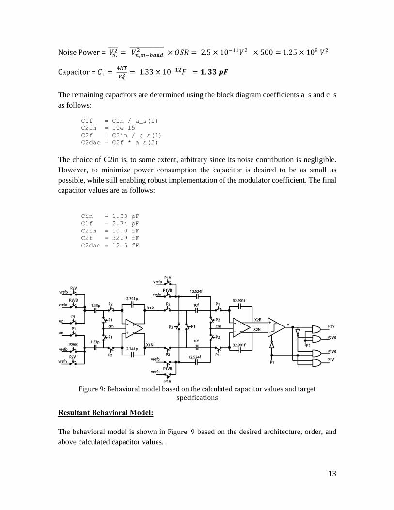
The remaining capacitors are determined using the block diagram coefficients a_s and c_s as follows:
C1f = Cin / a_s(1) C2in = 10e-15 C2f = C2in / c_s(1) C2dac = C2f * a_s(2)
The choice of C2in is, to some extent, arbitrary since its noise contribution is negligible. However, to minimize power consumption the capacitor is desired to be as small as possible, while still enabling robust implementation of the modulator coefficient. The final capacitor values are as follows:
Cin = 1.33 pF C1f = 2.74 pF C2in = 10.0 fF C2f = 32.9 fF C2dac = 12.5 fF
Figure9:Behavioralmodelbasedonthecalculatedcapacitorvaluesandtarget
specifications
Resultant Behavioral Model: The behavioral model is shown in Figure 9 based on the desired architecture, order, and above calculated capacitor values.

14
In order to obtain the desired results, you need to consider the followingrequirements: For the fully differential op‐amp: DC gain > 60dB
For the fully differential op‐amp: unity gain frequency =~ 10* Sampling Frequency
For Ts in the simulation file: set to be at least 20 times the op‐amp unity gain
bandwidth
The time constant of the sampling switched capacitors need to be significantly
greater than Ts (i.e., the time step of the simulator specified in the test.par file). In
particular, the bandwidth 1/(2RC), where R is the resistance of the switch and C is the capacitor it charges, should be at least 20 times lower than 1/Ts. If this
condition is not met, the simulated kT/C noise of the given switched capacitor
network will generally be lower than its true value, and therefore yield incorrect
noise simulation results.
Given the above, theprevious schematicwill be simulatedusingCppSimwith thefollowingspecifications:
Parameter Value Input Signal Frequency 300 Hz
Input Signal Amplitude (Vp-p)(-3dBFS) 0.707 V Sampling Frequency 1MHz
Fully Diff. Opamp DC gain 90dB Fully Diff. Opamp unity gain frequency 10MHz
PreliminariesA.OpeningSue2Schematics Click on the Sue2 icon to start Sue2, and then select the Sigma_delta_ord2_dt_adc_examplelibrary from the schematiclistbox.
Select the second_order_dt_sigma_delta_adc cell from the above schematic listbox. The Sue2 schematic window should now appear as shown below. Key signals for this schematic include: up,un: analog differential input of the ADC (positive and negative sides respectively) s1p, s1n: differential output of the first stage of the ADC (positive and negative sides respectively)

15
s2p, s2n: differential output of the second stage of the ADC (positive and negative sides respectively) v: digital output of the ADC v_filt: output of the second order Butterworth filter that takes output signalvasinputp1,p2:non‐overlappingclocksignalsp1b,p2b:invertedversionofthenon‐overlappingclocksignalsintheADCp1v,p1vb,p2v,p2vb:controlsignalsforswitchesinADCvp,vn:referencevoltagesforthe ADC (positive and negative sides respectively) cm:commonmodevoltageofthedifferentialoperationalamplifier
B.RunningCppSimSimulations In the Sue2 schematic window, click on the Tools text box in the menu bar, and then select CppSim Simulation. A Run Menu window similar to the one shown below should open automatically. Note that the Run Menu is already synchronized to the schematic that you will be simulating (second_order_dt_sigma_delta_adc). If for whatever reason this is not the case, click on the Synchronize button in the menu bar, the Run Menu will be synchronized to the schematic in your Sue2 window.

16
To establish the simulation parameters, click on the Edit Sim File button in the menu. An Emacs window should appear displaying the contents of the simulation parameters file (test.par). The contents of your test.par file should look something like what is shown below: ///////////////////////////////////////////////////////////// // CppSim Sim File: test.par // Cell: second_order_dt_sigma_delta_adc // Library: Sigma_delta_ord2_dt_adc_example ///////////////////////////////////////////////////////////// ///////////////////////////////////////////////////////////// // Number of simulation time steps // Example: num_sim_steps: 10e3 num_sim_steps: 2e6 // Time step of simulator (in seconds) // Set to be 20 times the opamp unity gain bandwidth of op-amp Ts: 1/(20*10e6) // Output File name // Example: name below produces test.tr0, test.tr1, ... // Note: you can decimate, start saving at a given time offset, etc.

17
// -> See pages 34-35 of CppSim manual (i.e., output: section) output: test end_sample=10e6 // Nodes to be included in Output File // Example: probe: n0 n1 xi12.n3 xi14.xi12.n0 probe: vin v s1p s2p s1n s2n up un p1 p2 v_filt //output: test_out trigger=p1 start_time=1e-6 //probe: v ///////////////////////////////////////////////////////////// // Note: Items below can be kept unaltered if desired ///////////////////////////////////////////////////////////// // Numerical integration method for electrical schematics // 1.0: Backward Euler (default) // 0.0: Trap (more accurate, but prone to ringing) electrical_integration_damping_factor: 1.0 // Values for global nodes used in schematic // Example: global_nodes: gnd=0.0 avdd=1.5 dvdd=1.5 global_nodes: gnd = 0.0 // Values for global parameters used in schematic // Example: global_param: in_gl=92.1 delta_gl=0.0 step_time_gl=100e3*Ts global_param: ktc_en = 0 // Rerun simulation with different global parameter values // Example: alter: in_gl = 90:2:98 // See pages 37-38 of CppSim manual (i.e., alter: section) alter: When you are finished, you can close the Emacs window by pressing Ctrl-x Ctrl-c. Tolaunchthesimulation,clickonthemenubarbuttonlabeledCompile/Run. PlottingTime‐DomainResults Double‐clickontheCppSimViewicontostarttheCppSimviewer.Theviewershouldappear as shown below – notice that the banner indicates that it is currentlysynchronizedtothesecond_order_dt_sigma_delta_adc cellview. If this isnot thecase, Sue2andCppSimViewcanbe synchronizedby clicking theSynch buttonontheleft‐handsideoftheCppSimViewwindow.

18
Toviewthesimulationresults,firstclickontheradiobuttontitledNoOutputFile.Immediately after this button is clicked, the radio buttonwill instead display theoutputfile’sname,test.tr0. Next,clickontheLoadbuttonontheleft‐handsideoftheCppSimViewwindow.Oncethisbuttonispressed,theNodesradiobuttonwillbefilledin,andtheprobednodeswillbelisted,asshownbelow.
A.OutputSignalPlotsThe input data is up-un is at frequency of 300Hz with a Vp-p of 0.707V. The clock signals p1, p2 are at frequency of 1MHz. To view the important signals you can select their names from the window as shown below. Note that you can use a comma to plot signals on the same subplot (as done for signals p1 and p2 in the example below), and operators such as minus in order to plot the difference in signals (as done for signals s1p-s1n and s2p-s2n in the example below).

19
To change the x-axis of the figure (the y-axis automatically scales), hit the Zoom radio button on the CppSimView menu-bar. This will cause a series of buttons to appear on the top and bottom of the plot window, as shown below.

20
Next click the (Z)oom X push-button located at the top of the plot window. Select the desired x-axis range by clicking at the beginning and ending location in any of the plotted signals. The figure will look similar to the figure below. Additionally, you can zoom in and out and pan left and right using the Inand Outand the <and >push-buttons, respectively, located at the top of the plot figure.

21
SinceweplacedasecondorderButterworthlowpassfilterattheoutputweareabletoexaminethefilteredversionoftheoutput,v_filt,andcomparetotheinput,vin,asshowninthefigurebelow.

22
B.MatlabVerificationofOutputSpectrumForthisexerciseweleveragetheMatlabtoolbox“HspiceToolboxforMatlabandOctave” which is part of the CppSim package. Hspice Toolbox for Matlab® andOctaveisacollectionofMatlab®/OctaveroutinesthatallowtheusertomanipulateandviewsignalsgeneratedbyHspice,Ngspice,andCppSimsimulations.Toverifytheperformanceofthesimulated“second_order_dt_sigma_delta_adc”,youneed to run the simulation for a longer duration using the simulation file below.Afterthecompletionofthisstep,“test_out.tr0”filewillbegeneratedinthefollowingdirectory:C:\CppSim\SimRuns\Sigma_delta_ord2_dt_adc_example\second_order_dt_sigma_delta_adcFortheverificationofPSDplotsandSNRvalue,wewillruntheMatlabverificationcodeshowninAppendixBas“calculate_snr.m”file.whichisalsolocatedinsidetheabovedirectory.RunningthisscriptwithintheMatlabenvironmentthengeneratesthePSDplotsandcalculatesthecorrespondingSNRvalue.However,wefirstneedtogeneratethe“test_out.tr0”file,whichisachievedbyupdatingthesimulationfileasshownbelow(withchangesinred)andthenre‐runningCppSim.
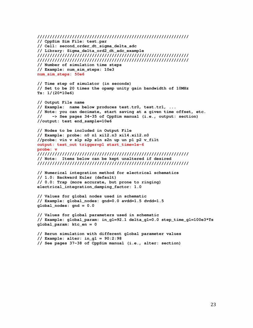
23
///////////////////////////////////////////////////////////// // CppSim Sim File: test.par // Cell: second_order_dt_sigma_delta_adc // Library: Sigma_delta_ord2_dt_adc_example ///////////////////////////////////////////////////////////// ///////////////////////////////////////////////////////////// // Number of simulation time steps // Example: num_sim_steps: 10e3 num_sim_steps: 50e6 // Time step of simulator (in seconds) // Set to be 20 times the opamp unity gain bandwidth of 10MHz Ts: 1/(20*10e6) // Output File name // Example: name below produces test.tr0, test.tr1, ... // Note: you can decimate, start saving at a given time offset, etc. // -> See pages 34-35 of CppSim manual (i.e., output: section) //output: test end_sample=10e6 // Nodes to be included in Output File // Example: probe: n0 n1 xi12.n3 xi14.xi12.n0 //probe: vin v s1p s2p s1n s2n up un p1 p2 v_filt output: test_out trigger=p1 start_time=1e-6 probe: v ///////////////////////////////////////////////////////////// // Note: Items below can be kept unaltered if desired ///////////////////////////////////////////////////////////// // Numerical integration method for electrical schematics // 1.0: Backward Euler (default) // 0.0: Trap (more accurate, but prone to ringing) electrical_integration_damping_factor: 1.0 // Values for global nodes used in schematic // Example: global_nodes: gnd=0.0 avdd=1.5 dvdd=1.5 global_nodes: gnd = 0.0 // Values for global parameters used in schematic // Example: global_param: in_gl=92.1 delta_gl=0.0 step_time_gl=100e3*Ts global_param: ktc_en = 0 // Rerun simulation with different global parameter values // Example: alter: in_gl = 90:2:98 // See pages 37-38 of CppSim manual (i.e., alter: section)

24
Results:OutputPSDandSNRAfter running CppSim with the updated simulation file, run the Matlab script“calculate_snr.m”withintheabovedirectorytoseetheplotsshownbelow.Figure10showstheoutputpowerspectradensitywheretheSNRis101.5dB,whichiswithin0.5dBofthematlabsimulationsunderthesameconditions.CppSim provides a feature that allows for noise simulation to account for thethermalnoiseintroducedbytheswitcheswhichmanifestsitselfintheformofKT/Cnoise. This is accomplished by setting the global parameter ktc_en to 1 in the“test.par”file.Moregenerallythisisachievedbysettingthenoise_enableparametertooneinthecellelectrical_switchfromthelibraryElectrical_Examples.Theresultingpowerspectraldensity isshowninFigure11wheretheSNRisnow98.4dB. Ifweconsider that the3rdharmonic is ‐102.6dBFS,wecalculate theSNRexcluding the 3rd harmonic to be 100dB which agrees with our theoreticalcalculations.
Figure10CppSimbehavioralsimulationofthemodulatorproducesa101.5dBSNRanda3rdharmonicat‐102dBFS.
101
102
103
104
105
-200
-180
-160
-140
-120
-100
-80
-60
-40
-20
0CppSim Output PSD
Frequency (Hz)
dB
FS
/NB
W
SNR = 101.5dB3rd harmonic = -102.0dBFS

25
Figure11CppSimsimulationwithKT/CnoiseenabledproducesaSNRequalto98.4dB
ConclusionThis tutorial covers the basic issues related to the behavioral simulation of a simple Second Order Discrete Time Delta Sigma ADC design example using CppSim and Matlab. In particular, the reader has been introduced to the tasks of running CppSim simulations, plotting output signals as well as performing Matlab synthesis and verifications. Finally, the agreement of SNR values between the initial Matlab synthesis and final CppSim simulation results of the design example has been verified which reflects the importance of CppSim in simulating and understanding the behavior of Delta Sigma ADCs.
References
1- Understanding Delta-Sigma Data Converters, Richard Schreier & Gabor C. Temes 2- “EXAMPLE DESIGN– PART 1”, Lecture 3, Richard Schreier & Trevor Caldwell,
ECE1371 Advanced Analog Circuits, http://individual.utoronto.ca/schreier/lectures/2012/3-2.pdf
3- Wern Ming Koe; Jing Zhang; , "Understanding the effect of circuit non-idealities on sigma-delta modulator," Behavioral Modeling and Simulation, 2002. BMAS 2002. Proceedings of the 2002 IEEE International Workshop on , vol., no., pp. 94- 101, 6-8 Oct. 2002 URL: http://ieeexplore.ieee.org/stamp/stamp.jsp?tp=&arnumber=1291065&isnumber=28751
101
102
103
104
105
-200
-180
-160
-140
-120
-100
-80
-60
-40
-20
0CppSim Output PSD
Frequency (Hz)
dB
FS
/NB
W
SNR = 98.4dB3rd harmonic = -102.6dBFS

26
AppendixA:MatlabSynthesisCodeclear all; addpath('C:\Program Files\MATLAB\R2012b\toolbox\delsig') %--------------------------------------------------- % Design Parameters order = 2; % Filter order OSR = 500; % OSR Fs = 1e6; % Sampling Frequency N = 100e3; % Number of Points opt = 0; % Optimization (=1 for odd order) H_inf = 1.5; % Maximum out of band gain of NTF, should be less than 2 f0 = 0; % Lowpass design form = 'CRFB'; % Cascaded Resonator, Feed Back with delaying element nlev = 2; % Quantization Levels fs = 1; % Normalized Sampling Frequency In_FS = sqrt(2); % Full-Scale Input SNR_target = 100; % 100dB SNR target for full-scale input %--------------------------------------------------- % Synthesis and Dynamic Range Scaling % Noise Transfer Function ntf = synthesizeNTF(order,OSR,opt,H_inf,f0); % CRFBD model, coefficients realization [a,g,b,c] = realizeNTF(ntf,form); % ABCD matrix calculation ABCD = stuffABCD(a,g,b,c,form); % Scale the state variable maximum to 0.707 [ABCDs,umax] = scaleABCD(ABCD,nlev,0.707); % Noise and signal transfer function [ntf2,stf] = calculateTF(ABCD,1); % Generate CRFB Coefficients [a_s,g_s,b_s,c_s] = mapABCD(ABCDs,form); b_s(2:3)=0; % This step simplifies how the input is applied to the DSM %--------------------------------------------------- % Simulate Full Scale Input at Frequency 30*Fs/N t = [0:(N-1)]/Fs; u = In_FS/2 * sin(t*2*pi*Fs/N*30); %Simulate the output [v,xn,xmax,y] = simulateDSM(u,ABCDs,nlev); %Plotting figure(1)

27
plot(t,v,'LineWidth',1); hold on plot(t,u,'r','LineWidth',3); hold off xlim([0.001 0.0025]) ylim([-1.5 1.5]) title('Time Domain Signal Response','Fontsize',12); xlabel('Time (sec)','Fontsize',12); ylabel('Amplitude(V)','Fontsize',12); legend('Output Signal','Input Signal'); grid on print -dtiff 'figures/matlab_uv' print -dmeta 'figures/matlab_uv' xlim([0.0015 0.0016]) print -dtiff 'figures/matlab_uv_zoom' print -dmeta 'figures/matlab_uv_zoom' figure(2) plot(t,xn(1,:),t,xn(2,:),'LineWidth',1); xlim([0 0.02]) ylim([-1.0 1.0]) title('Time Domain Signal Response','Fontsize',12); xlabel('Time (sec)','Fontsize',12); ylabel('Amplitude(V)','Fontsize',12); legend('x1','x2'); grid on print -dtiff 'figures/matlab_x1x2' print -dmeta 'figures/matlab_x1x2' %--------------------------------------------------- % Output PSD and SNR wind_hann = hann(N,'periodic'); % Hanning Window v_hann = v .* wind_hann'; % Windowed Input % Sin-wave scaled PSD (see page 372 in Schreier and Temes) S_vv = ( abs( fft(v_hann,N) / ((sum(wind_hann) * In_FS/4))) ).^2; %Calculating SNR signal_bins = find(S_vv > max(S_vv)/4.1); signal_power = sum(S_vv(signal_bins)); noise_power = 2*sum(S_vv(1:length(S_vv)/2/OSR)) - signal_power; snr_value = 10*log10(signal_power/noise_power) hd3 = 10*log10(abs(S_vv(signal_bins(2)*3-2))) %Frequency axis f = Fs/2*linspace(0,1,N/2); figure(3) clf semilogx(f,10*log10(S_vv(1:N/2)),'b','LineWidth',2) xlim([10 500e3]) ylim([-200 0]) title('Output PSD','Fontsize',12); xlabel('Frequency (Hz)','Fontsize',12); ylabel('dBFS/NBW','Fontsize',12); text(3e3,-160,sprintf('SNR = %4.1fdB\n',snr_value))

28
text(3e3,-170,sprintf('3rd harmonic = %4.1fdBFS\n',hd3)) print -dtiff 'figures/matlab_psd' print -dmeta 'figures/matlab_psd' %--------------------------------------------------- % Simulate SNR vs Input Amplitude [snr,amp] = simulateSNR(ntf,OSR,[-120:20:-20 -10:-2],f0,nlev,1/(4*OSR),13); [snr2,amp2] = predictSNR(ntf,OSR); figure(4) plot(amp,snr,'ro','linewidth',2); hold on plot(amp2,snr2,'k-x','linewidth',2); hold off title('SNR vs Amplitude','Fontsize',12); xlabel('Input Level (dB)','Fontsize',12); ylabel('SNR (dB)','Fontsize',12); legend('Simulated SNR','Predicted SNR','Location','Best'); grid on text(-99,105,sprintf('peak SNR = %4.1fdB\n',max(snr))) print -dtiff 'figures/matlab_snr_vs_amp' print -dmeta 'figures/matlab_snr_vs_amp' figure(5) %plotPZ(ntf,'r') plot(real(ntf.p{:}),imag(ntf.p{:}),'Xk','Markersize',12,'linewidth',2); hold on plot(real(ntf.z{:}),imag(ntf.z{:}),'Or','Markersize',12,'linewidth',2) plot(exp(j*2*pi*[0:0.01:1]),'linewidth',2) axis([-1.2 1.2 -1 1]) title('NTF Pole-Zero Plot','Fontsize',12); print -dtiff 'figures/matlab_pz' print -dmeta 'figures/matlab_pz' %--------------------------------------------------- % Compute Capacitor Values k = 1.38e-23; % Boltzman's constant (J/K) T = 300; % Temperature in Kelvin (K) Cin = 4*k*T/((In_FS/2)^2/2/10^(SNR_target/10) ) / OSR C1f = Cin/a_s(1) C2in = 10e-15 C2f = C2in/c_s(1) C2dac = C2f*a_s(2) %Cin = 1.33e-12 %C1f = 2.7303e-12 %C2f = 3.2901e-14 %C2dac = 1.2524e-15

29
AppendixB:MatlabVerificationCode(calculate_snr.m)clear; % Include HspiceToolbox if ispc ==1 addpath('c:\CppSim\CppSimShared\HspiceToolbox\'); else addpath('~/CppSim/CppSimShared/HspiceToolbox'); end cd C:\CppSim\SimRuns\Sigma_delta_ord2_dt_adc_example\second_order_dt_sigma_delta_adc %--------------------------------------------------- % Input Parameters N = 1e5; % Number of points for FFT Fs = 1e6; % Sampling frequency fin = 1e3; % Input signal bandwidth OSR = Fs/2/fin; % Oversampling ratio OSR = 500; % Oversampling ratio In_FS = sqrt(2); % Input full-scale f = Fs/2*linspace(0,1,N/2); % Frequency axis %--------------------------------------------------- % Load simulation results % Load the simulation file x = loadsig_cppsim('test_out.tr0'); %x = loadsig_cppsim('test.tr0'); % Extract the output signal v vl = evalsig(x,'v'); v = vl(length(vl)-N+1:length(vl))'; %--------------------------------------------------- % Output PSD and SNR wind_hann = hann(N,'periodic'); % Hanning Window v_hann = v .* wind_hann'; % Windowed Input % Sin-wave scaled PSD (see page 372 in Schreier and Temes) S_vv = ( abs( fft(v_hann,N)) / ((sum(wind_hann) * In_FS/4)) ) .^2; %Calculating SNR signal_bins = find(S_vv > max(S_vv)/4.1); signal_power = sum(S_vv(signal_bins)); noise_power = 2*sum(S_vv(1:length(S_vv)/2/OSR)) - signal_power; snr_value = 10*log10(signal_power/noise_power) hd3 = 10*log10(abs(S_vv(signal_bins(2)*3-2))) %Frequency axis f = Fs/2*linspace(0,1,N/2);

30
figure(3) clf semilogx(f,10*log10(S_vv(1:N/2)),'LineWidth',2) axis([10 500e3 -200 0]) title('CppSim Output PSD','Fontsize',12); xlabel('Frequency (Hz)','Fontsize',12); ylabel('dBFS/NBW','Fontsize',12); text(3e3,-160,sprintf('SNR = %4.1fdB\n',snr_value)) text(3e3,-170,sprintf('3rd harmonic = %4.1fdBFS\n',hd3)) print -dtiff 'figures/cppsim_psd' print -dmeta 'figures/cppsim_psd'