benefits given by r60xxjnx series for the phase-shift full ... · the leakage inductance of the...
TRANSCRIPT
1/9
© 2017 ROHM Co., Ltd. No. 60AP001E Rev.001
2017.4
© 2018 ROHM Co., Ltd. No. 61AN029E Rev.001
JULY.2018
Application Note
Super Junction MOSFET series
Benefits given by R60xxJNx series for the
Phase-Shift Full-Bridge
The full-bridge configuration is utilized for power supplies such as server power sources, on-board chargers, and many other power
electronic applications. In particular, the phase-shift full-bridge circuit (PSFB) enlarges its power supply capability through reduced
switching losses, because this circuit topology allows the adoption of zero-voltage switching (ZVS) techniques for switching devices
such as SJMOS and IGBTs. This application note explains how the PSFB equipped with SJMOS’s operates, and also elucidates why
SJMOS in the PSFB must have high-speed recovery capability for its body diode (BD). In addition, this document provides the
measurement results of power conversion efficiency for the PSFB including ROHM’s PrestoMOSTM and competitor’s SJMOS, and
finally proves that our R60xxJNx series realizes the best power conversion efficiency of the PSFB.
Basic Circuit Configuration of PSFB
Figure 1 shows the fundamental schematic of the PSFB. The leakage inductance of the transformer working as the resonant inductor
enables ZVS, while an additional inductor is often serially connected to the transformer in order to expand the ZVS operating area.
The PSFB in this application note always includes this kind of additional inductor, Ls.
Figure 1. Fundamental schematic of PSFB
Figure 2 shows the ON/OFF timing chart of switch Q1 to Q4.
The numbers at the bottom of the figure label represent the
specific operation modes of the circuit. As shown in this
diagram, the ON/OFF timing of Q3 and Q4 always comes after
the ON/OFF timing of Q1 and Q2 with a specific phase delay.
Thus, in general, the leg of Q1 and Q2 is named the leading leg,
while the leg of Q3 and Q4 is named the lagging leg.
Figure 2. Switching time charts for Q1 to Q4

2/9
Application Note Benefits given by R60xxJNx series for the Phase-Shift Full-Bridge
© 2018 ROHM Co., Ltd. No. 61AN029E Rev.001
JULY.2018
Basic Operation of PSFB
ZVS in PSFB is achieved by turning on a MOSFET with a forward current flowing through its body diode (BD) so that its output
capacitance of the MOSFET (Coss) is fully discharged.
Figure 3 includes the waveforms of drain current (ID) of Q1 to Q4 as well as the current flowing through the primary-side
transformer (IL) under normal operating conditions. The direction of drain-to-source is defined as the positive direction of ID here, and
you can easily find the period that minus ID flows in each Q1 to Q4 with its BD being forward biased. During this period, the drain
voltage is nearly zero, leading to ZVS if the MOSFET is turned on.
Figure 3. ID for Q1 to Q4 (ID_Q1, ID_Q2, ID_Q3, ID_Q4), and IL.
As you can see in Figure 3, the current waveforms are not the same for the leading and lagging leg in spite of the same operating
pattern. You can get the picture of why the waveforms differ by grasping how current flows in mode (1)-(14) defined in Figure 2 and 3.
The following Figure 4 to 7 explain current path step-by-step for each mode, for a better understanding of the waveforms in Figure 3.
Figure 4. The Current path in Mode (1) - (2)
Mode (1)
・Q1 and Q4 are on-state, whereas Q2 and Q3 are off-state.
・The off-state of Q2 and Q3 means that the output
capacitance of Q2 (Coss_Q2) and of Q3 (Coss_Q3) are fully
charged.
・Vi is applied to the primary side of the transformer.
・The energy is stored in Ls by the current flowing through it.
Mode (2)
・Q1 turns off.
・The output capacitance of Q1 (Coss_Q1) is being charged. Due
to this, the drain-side voltage of Q2 drops, which triggers
discharging of Coss_Q2.

3/9
Application Note Benefits given by R60xxJNx series for the Phase-Shift Full-Bridge
© 2018 ROHM Co., Ltd. No. 61AN029E Rev.001
JULY.2018
Figure 5. The Current path in Mode (3) - (7)
Mode (3)
・ If Ls still holds the energy after charging Coss_Q1 and
discharging Coss_Q2 are completed, the BD of Q2 (DQ2) is
forward biased, starting its freewheeling phase.
・In the freewheeling period, the energy isn’t delivered to the
secondary side. However, the current on secondary side
continues to flow due to Lo. So, the forward current flows
through D1 and D2.
Mode (4)
・Q2 turns on. At this point, DQ2 is on-state, and this means
that the drain-source voltage of Q2 (VDS_Q2) is almost zero.
Thus ZVS is achieved, leading to little turn-on loss.
Mode (5)
・Q4 turns off.
・The output capacitance of Q4 (Coss_Q4) is being charged. Due
to this, the source-side voltage of Q3 drops, which triggers
discharging of Coss_Q3.
Mode (6)
・ If Ls still holds the energy after charging Coss_Q4 and
discharging Coss_Q3 are completed, the BD of Q3 (DQ3) is
forward biased, starting freewheeling.
Mode (7)
・Q3 turns on. At this point, DQ3 is on-state, and this means
that the drain-source voltage of Q3 (VDS_Q3) is almost zero.
Thus ZVS is achieved, leading to little turn-on loss.
・This voltage direction makes current flow opposite to IL in
Mode (1) to (6), and consequently the current direction flips
rapidly.

4/9
Application Note Benefits given by R60xxJNx series for the Phase-Shift Full-Bridge
© 2018 ROHM Co., Ltd. No. 61AN029E Rev.001
JULY.2018
Figure 6. The Current path in Mode (8) - (12)
Mode (8)
・Q2 and Q3 are on-state, whereas Q1 and Q4 are off-state.
・The off-state of Q1 and Q4 means that Coss_Q1 and Coss_Q4
are fully charged.
・Vi is applied to the primary side of the transformer in the
opposite direction.
・The energy is stored in Ls by current flowing through it.
Mode (9)
・Q2 turns off.
・Coss_Q2 is being charged. This triggers discharging of Coss_Q1.
Mode (10)
・ If Ls still holds the energy after charging Coss_Q2 and
discharging Coss_Q1 are completed, the BD of Q1 (DQ1) is
forward biased, starting freewheeling.
・ In the freewheeling period, the energy isn’t delivered to
secondary-side. However, the current continues to flow due to
Lo. So, the forward current flows to D1 and D2.
Mode (11)
・Q1 turns on. At this point, DQ1 is on-state, and this means
that the drain-source voltage of Q1 (VDS_Q1) is almost zero.
Thus ZVS is achieved, leading to little turn-on loss.
Mode (12)
・Q3 turns off.
・Coss_Q3 is charged, while Coss_Q4 is discharged.

5/9
Application Note Benefits given by R60xxJNx series for the Phase-Shift Full-Bridge
© 2018 ROHM Co., Ltd. No. 61AN029E Rev.001
JULY.2018
Figure 7. The Current path in Mode (13) - (14)
As detailed in explanation for Mode (7) and (14), the turn-on of a MOSFET in the lagging leg causes the serial connection of the
input source and Ls, and thus the energy stored in Ls diminishes rapidly. This operation mode does not happen for the leading leg, and
consequently the waveforms differ between the leading and lagging leg. As explained for Mode (5), (6), (12), and (13), in the lagging
leg, if the energy stored in Ls is less than the one stored in Coss, a MOSFET cannot complete the charging and discharging process
and ZVS cannot be achieved. Hence, if Mode (5) is taken as an example, the condition to establish ZVS is expressed as equation (1).
1
2𝐿𝑠𝐼𝐿1
2 > 𝐸𝑜𝑠𝑠_𝑄3 + 𝐸𝑜𝑠𝑠_𝑄4
Where IL1 is IL at the point that Mode (4) completed, and Eoss_Q3, Eoss_Q4 is the energy necessary to charge the Coss of Q3 and Q4,
respectively.
Equation (1) shows that ZVS is not achieved for small IL1, namely light load, and also that it become easier to establish ZVS for
heavier load.
Remarks for device operation in the case of light load
As explained in details above, small current in light-load operation causes low energy storage in Ls, and consequently a MOSFET
in the lagging leg highly likely switches without completing its charging and discharging process. This results in no ZVS operation
and consequently increases the turn-on loss of the MOSFET.
On the other hand, MOSFETs in the leading leg transfer energy to the secondary side through the transformer during their charging
and discharging transitions. Similar consideration for deriving equation (1), if we take Mode (2) as an example, leads to the
condition to achieve ZVS in the leading leg as:
1
2(𝐿𝑠 + 𝑛2𝐿𝑜)𝐼𝐿2
2 > 𝐸𝑜𝑠𝑠_𝑄1 + 𝐸𝑜𝑠𝑠_𝑄2
Where n is the turns ratio of the transformer, IL2 denote IL at the final stage of Mode (1), Eoss_Q1
and Eoss_Q2 defines the energy necessary
to charge or discharge Coss of Q2, respectively.
Setting of the dead time is needed to avoid short circuit of high-side and low-side arms for practical circuit operation. On the other
hand, VDS, as mentioned above, possibly remains non-zero under a light load condition due to incompletion of discharging the
Mode (13)
・ If Ls still holds the energy after charging Coss_Q3 and
discharging Coss_Q4 are completed, the BD of Q4 (DQ4) is
forward biased, starting freewheeling.
Mode (14)
・Q4 turns on. At this point, DQ4 is on-state, and this means
that the drain-source voltage of Q4 (VDS_Q4) is almost zero.
Thus ZVS is achieved, leading to little turn-on loss.
・This voltage direction makes current flow opposite to IL in
Mode (8) to (13), and consequently the current direction flips
rapidly.
(1)
(2)
6/9
Application Note Benefits given by R60xxJNx series for the Phase-Shift Full-Bridge
© 2018 ROHM Co., Ltd. No. 61AN029E Rev.001
JULY.2018
MOSFETs in the lagging leg. This means on the other side that some dead-time settings could increase the possibility of not
achieving ZVS at light load operation. Therefore the duration of dead time should be adjusted carefully.
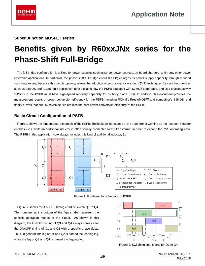
Figure 8 qualitatively illustrates the turn-on transient waveforms of VDS and ID for an optimized and non-optimized dead-time setting
case.
Figure 8. Simplified turn-on transient waveforms of VDS and ID of a MOSFET in the lagging leg.
Figure 8 also shows that for a non-optimized dead-time case, a large ID instantaneously flows. This current has two components:
a short-circuit current caused by the gate-source voltage (VGS) exceeding its threshold [1], and the current to charge the Coss of the
MOSFET in the other arm. This latter part is unavoidable for hard-switching operation, but you can prevent the former one by tuning
appropriately the ratio of Cgd to Cgs, where Cgd and Cgs denote the gate-drain and gate-source capacitance of the MOSFET
respectively.
PrestoMOSTM can suppress the short-circuit current by tuning the ratio of Cgd/Cgs, and thus low power loss, namely high efficiency
can be achieved.
Remarks for device operation in the case of heavy load
MOSFETs likely fail by unintentional triggering of the parasitic bipolar transistor embedded in a MOSFET in the leading leg, if trr of
the BD is large in the case of heavy load [1]. This spontaneous turn-on is caused by the current charging the drain-source capacitance
Cds when MOSFETs turn off, and thus this bipolar-oriented instantaneous large current triggers the fatal accident.
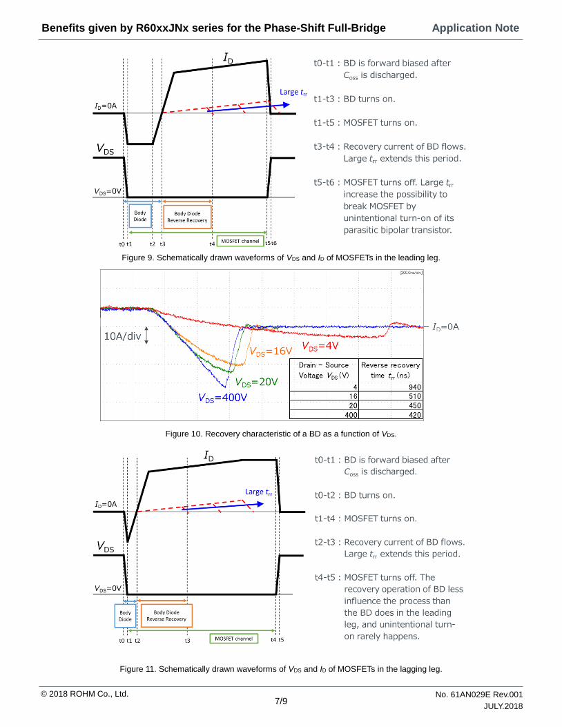
In an inverter circuit, the charge stored in a BD (Qrr) is forcefully and quickly evacuated by the high-voltage reverse bias applied
during the turn-off of the BD. The time necessary to evacuate these charges is trr, which kept small in this case. On the other hand, as
shown in Figure 9, the voltage applied to a BD is nearly zero during its recovery in PSFB, and therefore the stored charge needs
longer to be evacuated, leading to a larger trr. Figure 10 provides experimental waveforms for this phenomenon. It includes the reverse
recovery current waveforms of conventional SJMOS for different drain-source voltages.
A decreasing VDS and, hence a larger trr shifts the reverse recovery current as shown by the red dotted lines in Figure 9. As a result,
large trr means a large amount of charges in the MOSFET during its turning off, and in this case current easily flow through the
MOSFET, increasing the possibility to turn on the parasitic bipolar transistor.
7/9
Application Note Benefits given by R60xxJNx series for the Phase-Shift Full-Bridge
© 2018 ROHM Co., Ltd. No. 61AN029E Rev.001
JULY.2018
Figure 9. Schematically drawn waveforms of VDS and ID of MOSFETs in the leading leg.
Figure 10. Recovery characteristic of a BD as a function of VDS.
Figure 11. Schematically drawn waveforms of VDS and ID of MOSFETs in the lagging leg.
8/9
Application Note Benefits given by R60xxJNx series for the Phase-Shift Full-Bridge
© 2018 ROHM Co., Ltd. No. 61AN029E Rev.001
JULY.2018
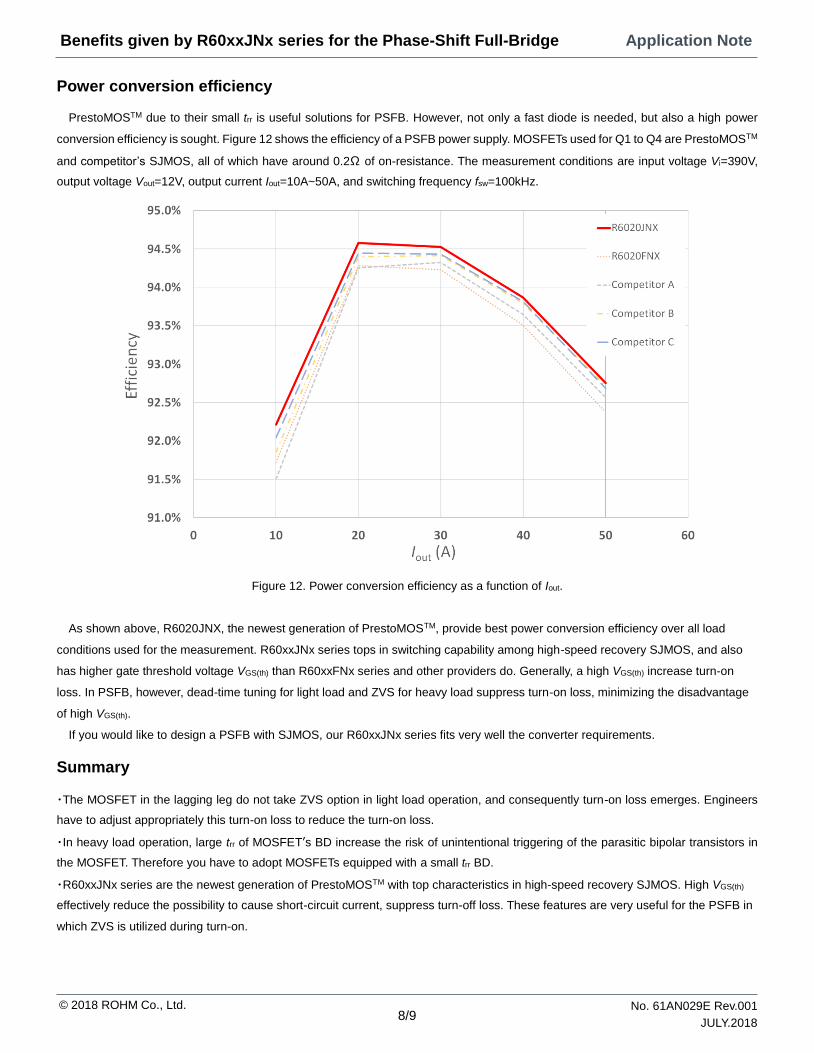
Power conversion efficiency
PrestoMOSTM due to their small trr is useful solutions for PSFB. However, not only a fast diode is needed, but also a high power
conversion efficiency is sought. Figure 12 shows the efficiency of a PSFB power supply. MOSFETs used for Q1 to Q4 are PrestoMOSTM
and competitor’s SJMOS, all of which have around 0.2Ω of on-resistance. The measurement conditions are input voltage Vi=390V,
output voltage Vout=12V, output current Iout=10A~50A, and switching frequency fsw=100kHz.
Figure 12. Power conversion efficiency as a function of Iout.
As shown above, R6020JNX, the newest generation of PrestoMOSTM, provide best power conversion efficiency over all load
conditions used for the measurement. R60xxJNx series tops in switching capability among high-speed recovery SJMOS, and also
has higher gate threshold voltage VGS(th) than R60xxFNx series and other providers do. Generally, a high VGS(th) increase turn-on
loss. In PSFB, however, dead-time tuning for light load and ZVS for heavy load suppress turn-on loss, minimizing the disadvantage
of high VGS(th).
If you would like to design a PSFB with SJMOS, our R60xxJNx series fits very well the converter requirements.
Summary
・The MOSFET in the lagging leg do not take ZVS option in light load operation, and consequently turn-on loss emerges. Engineers
have to adjust appropriately this turn-on loss to reduce the turn-on loss.
・In heavy load operation, large trr of MOSFET’s BD increase the risk of unintentional triggering of the parasitic bipolar transistors in
the MOSFET. Therefore you have to adopt MOSFETs equipped with a small trr BD.
・R60xxJNx series are the newest generation of PrestoMOSTM with top characteristics in high-speed recovery SJMOS. High VGS(th)
effectively reduce the possibility to cause short-circuit current, suppress turn-off loss. These features are very useful for the PSFB in
which ZVS is utilized during turn-on.

9/9
Application Note Benefits given by R60xxJNx series for the Phase-Shift Full-Bridge
© 2018 ROHM Co., Ltd. No. 61AN029E Rev.001
JULY.2018
References
[1] L. Saro, et al., “High-Voltage MOSFET Behavior in Soft-Switching Converter: Analysis and
Reliability Improvements,” International Tel-communication Conference, San Francisco, 1998.

6
Notice
ROHM Customer Support System http://www.rohm.com/contact/
Thank you for your accessing to ROHM product informations. More detail product informations and catalogs are available, please contact us.
N o t e s
The information contained herein is subject to change without notice.
Before you use our Products, please contact our sales representative and verify the latest specifica-tions :
Although ROHM is continuously working to improve product reliability and quality, semicon-ductors can break down and malfunction due to various factors.Therefore, in order to prevent personal injury or fire arising from failure, please take safety measures such as complying with the derating characteristics, implementing redundant and fire prevention designs, and utilizing backups and fail-safe procedures. ROHM shall have no responsibility for any damages arising out of the use of our Poducts beyond the rating specified by ROHM.
Examples of application circuits, circuit constants and any other information contained herein are provided only to illustrate the standard usage and operations of the Products. The peripheral conditions must be taken into account when designing circuits for mass production.
The technical information specified herein is intended only to show the typical functions of and examples of application circuits for the Products. ROHM does not grant you, explicitly or implicitly, any license to use or exercise intellectual property or other rights held by ROHM or any other parties. ROHM shall have no responsibility whatsoever for any dispute arising out of the use of such technical information.
The Products specified in this document are not designed to be radiation tolerant.
For use of our Products in applications requiring a high degree of reliability (as exemplified below), please contact and consult with a ROHM representative : transportation equipment (i.e. cars, ships, trains), primary communication equipment, traffic lights, fire/crime prevention, safety equipment, medical systems, servers, solar cells, and power transmission systems.
Do not use our Products in applications requiring extremely high reliability, such as aerospace equipment, nuclear power control systems, and submarine repeaters.
ROHM shall have no responsibility for any damages or injury arising from non-compliance with the recommended usage conditions and specifications contained herein.
ROHM has used reasonable care to ensur the accuracy of the information contained in this document. However, ROHM does not warrants that such information is error-free, and ROHM shall have no responsibility for any damages arising from any inaccuracy or misprint of such information.
Please use the Products in accordance with any applicable environmental laws and regulations, such as the RoHS Directive. For more details, including RoHS compatibility, please contact a ROHM sales office. ROHM shall have no responsibility for any damages or losses resulting non-compliance with any applicable laws or regulations.
When providing our Products and technologies contained in this document to other countries, you must abide by the procedures and provisions stipulated in all applicable export laws and regulations, including without limitation the US Export Administration Regulations and the Foreign Exchange and Foreign Trade Act.
This document, in part or in whole, may not be reprinted or reproduced without prior consent of ROHM.
1)
2)
3)
4)
5)
6)
7)
8)
9)
10)
11)
12)
13)