bidirectional current-fed flyback-push-pull dc-dc converter · several isolated bidirectional...
TRANSCRIPT
BIDIRECTIONAL CURRENT-FED FLYBACK-PUSH-PULL DC-DCCONVERTER
Eduardo Valmir de Souza and Ivo BarbiPower Electronics Institute - INEP
Federal University of Santa Catarina - UFSCwww.inep.ufsc.br
[email protected], [email protected]
Abstract - This paper proposes a new dc-dc static powerconverter, designated Bidirectional Current-Fed Flyback-Push-Pull DC-DC Converter. Circuit operation, analysis,simulation, design example and experimental results areincluded in the paper. What distinguishes the proposedconverter from the previous circuits is the existence of in-put and output inductors, which provides a significant re-duction of both the power source and the load side currentripple. The proposed converter is suitable for the renew-able electric power systems, such as those having fuel cellsas the DC-source power supply. It is also a good candi-date for electric vehicle power systems, where bidirectionalpower flow related with battery charge and discharge isnecessary.
Keywords - bidirectional, current-fed, isolated, flyback-push-pull, dc-dc converter
I. INTRODUCTION
Fuel cells have been employed as primary power sourcein electrical vehicles since it presents high efficient and clearelectricity generation, however, it lacks energy storage capa-bility and fast power transient response [1]. Consequently, anauxiliary energy storage device is required such as lead-acidor lithium-ion battery.
Figure1 shows a fuel-cell-vehicle powertrain topology [2].
Fig. 1. : Fuel-cell-vehicle powertrain topology.
This system is composed by a low voltage fuel cell (LVFC),a low voltage battery (LVB), a double-layer capacitor bank(DLCB) and static converters. A low battery bank is em-ployed due to its volumetric efficiency comes down by con-necting several battery cells in series [3]. The LVB and DLCBcompose the energy-storage system. The capacitor will han-dle fast power transients like braking or accelerating whilethe battery will basically provide power at conditions that fuelcell presents low efficiency. Since this procedure avoids cur-rent surges to LVB, its lifetime will be extended [2]. A bidi-
rectional and an unidirectional DC-DC converter are neces-sary to interface the battery and fuel cell with the bus, re-spectively, because its output voltage change under operation.These converts can be isolated or non-isolated. Although non-isolated converters present fewer components, galvanic isola-tion is necessary when: high-voltage and low-voltage sourcesnegative poles cannot be connected or its voltage ratio is highenough that let semiconductors simultaneously handle highvoltage and current [4].
Several isolated bidirectional converter topologies havebeen studied to interface a low voltage battery bank to a highvoltage dc bus such as dual active bridge (DAB) types [5, 6]and current-fed half/full-bridge/push-pull types [7–10]. Fig-ures 2 (a) and (b) shows a DAB and a current-fed push-pulltopology, respectively.
Fig. 2. : (a) DAB and (b) current-fed push-pull.
The first type shows advantages such as first-order dy-namics, high-power density and few components [11, 12] butpresents the disadvantage of voltage source characteristics atboth sides. The second type presents current-fed at battery sidewhich let it drain low ripple current from the battery, protectslow voltage side transistors from current surge and transformerfrom unbalanced flux [13] when power flow direction is frombattery to dc bus. On the other hand, when reverse power flowis established, high voltage side transistors and transformer donot show such protections.
In this paper, a isolated bidirectional dc-dc current-fedtopology based on the unidirectional current-fed flyback-push-pull converter [14] will be proposed. Expected features are:
• Current-fed characteristic and low current ripple at bothsides;
978-1-4577-1646-1/11/$26.00 ©2011 IEEE 8

• reduced passive components and;• high-efficiency.
II. PROPOSED CONVERTER
Figure 3 shows the proposed converter topology. The con-verter is composed by:
• a flyback transformer, windings LFBp and LFBs;• a push-pull transformer, windings LPPp1, LPPp2, LPPs1
and LPPs2, and;• four bidirectional-current unidirectional voltage
switches, two for each side.
Both transformers have the same secondary-primary wind-ing turns ratio a.
Fig. 3. : Proposed bidirectional topology.
III. OPERATION MODES
The modulation strategy consists of commanding transis-tors Tp1 and Tp2 by two signals with duty cycle D and shiftedby half switching period. Ts1 and Ts2 commanding signals arecomplementary with Tp2 and Tp1 ones, respectively. Althoughit is required dead time between Tp1 and Ts2 and between Tp2and Ts1 signals, there is no need for dead time or overlappingfor transistor commanding signals from the same side. Dutycycle can vary from zero to one, hence, there are two operationmodes: one in which the primary transistor commanding sig-nals are non-overlapped, and another, in which they are. Sinceit is a bidirectional converter, for each mode mentioned before,there are two sub-modes depending on power flow directional.Table I presents these modes.
TABLE IOperation modes.
Power Flow 0 < D < 0, 5 0, 5 < D < 1
Primary to secondary Buckp→s Boostp→s
Secondary to primary Boosts→p Bucks→p
The subscriptions p and s indicate primary and secondarysides, respectively. The Buck and Boost analogy is used sinceproposed converter presents similar pulsed or continuous cur-rent characteristics at input or output.
Although there are four operation modes, only Buckp→s
and Boostp→s modes will be described due to converter input-output symmetry. Still, in the following description, switcheswill be considered ideal and transformers self inductance very
high. It will be described only the first half switching periodsince the other half is analogous. In the topological state illus-trations, a circle at the transistor gate will be used as symbolto represent that it is enabled.
A. Buckp→s Mode
First stage: The transistor Tp1 and Ts1 are enabled but dueto the current is direction, Ds1 conducts instead of Ts1. Tran-sistors Tp2 and Ts2 are disabled. Figure4 (a) shows this topo-logical state.
Second stage: At t = D · Ts, transistors Tp1 turns off, Ts2turns on and Tp2 and Ts1 keep the previous state. AlthoughTs1 and Ts2 states are both on, the current is flows throughDs1 and Ds2. Figure 4 (b) presents this topological state.
Fig. 4. : (a) First and (b) second stage in Buckp→s mode.
Figure 5 shows the main waveforms for the Buckp→s oper-ation mode.
Fig. 5. : Waveforms for Buckp→s mode.
B. Boostp→s Mode
First stage: The transistors Tp1 and Tp2 are enabled and halfof current ip flows through each one. Transistors Ts1 and Ts2are disabled. Figure 6(a) presents the topological state in thisstage.
9

Second stage: In t = (2D − 1)Ts/2, transistor Tp2 turnsoff and transistor Ts1 turns on. Although the transistor Ts1 isenabled, current is flows through Ds1 because of its direction.Figure 6(b) shows the topological state in the current stage.
Fig. 6. : (a) First and (b) second stage in Boostp→s mode.
Figure 7 presents the main waveforms for Boost p→s oper-ation mode.
Fig. 7. : Waveforms for Boostp→s mode.
IV. STATIC GAIN
Static gain is described by (1). Since the employed mod-ulation strategy lets the converter operate only in continuousconduction mode, this characteristic is independent of load.
EsEp
=a ·D1 −D
(1)
V. Passive components
The flyback primary winding self inductance and its nor-malized value are given by (2) and (3), respectively.
LFBp =Ep
2
Po · fs · ∆i%LFBp (2)
LFBp =
D2(1 − 2D)
2(1 −D)if 0 < D < 0.5
D(2D − 1)
2if 0.5 < D < 1
(3)
The secondary winding self inductance are given by (4).
LFBs = a2LFBp (4)
Equation (5) and (6) give the output capacitance and its nor-malized value, respectively.
Co =Po
Es2 · fs · ∆Vo%
Co (5)
Co =
D(1 − 2D)
2(1 −D)if 0 < D < 0.5
(2D − 1)
2if 0.5 < D < 1
(6)
Figure 8 shows the behavior of the normalized primarywinding inductance and output capacitance against duty cycle.
Fig. 8. : Normalized output capacitance and flyback induc-tance.
VI. SIMULATION RESULTS
The converter simulation will be realized to verify its oper-ation in the modes described in section III. Since both modestransfer power from the primary to secondary side, the outputvoltage source Es will be replaced by an RC load.
Table II shows two converter specifications design: one op-erating in Buckp→s mode and other in Boostp→s mode. TableIII presents the flyback transformer self inductances, transfor-mation ratio and output capacitance for each design.
TABLE IISpecification.
Description ValueInput Voltage 250 (V)
Output Voltage 250 (V)Nominal Power 2 (kW)
Switching Frequency 25 (kHz)Duty cycle 40; 60 (%)
Current Ripple 10 (%)Output voltage ripple 1 (%)
Figures 9 and 10 present Buckp→s and Boostp→s modesimulation results, respectively.
10

Fig. 9. : Simulation waveforms in Buckp→s mode.
Fig. 10. : Simulation waveforms in Boostp→s mode.
TABLE IIIConverter designs.
Parameter Buckp→s Boostp→s
a 1.5 0.67LFBp(µH) 333.3 750LFBs(µH) 750 333.3Co(µF) 8.5 12.8
VII. EXPERIMENTAL RESULTS
A laboratory prototype was implemented with the specifi-cation presented at Table IV. Two semi-regenerative clampingcircuits, one at primary side and another at secondary side,were designed due to the switches voltage stress producedby the interruption of transformer leakage inductance current.Figure 11 shows the converter schematic with the clampingcircuits.
TABLE IVPrototype specifications.
Parameter Valuea 2
Primary Side Voltage 80 (V)Secondary Side Voltage 160 (V)
Nominal Power 800 (W)Switching Frequency 50 (kHz)
Duty cycle 45; 55 (%)Current Ripple 10 (%)
Output voltage ripple 1 (%)LFBp 40 (µH)
LFBs 160 (µH)
Cp 940 (µF)
Cs 690 (µF)
Fig. 11. : Converter schematic with clamping circuit.
Experimental results were obtained for two operationmodes: Buckp→s and Boosts→p. Duty cycle was set at 45%for both cases. A 750 ns dead time was inserted between thetransistors Tp1 and Ts2 command signals and transistors Tp2and Ts1. For each mode, the output voltage source was re-placed by an RC load adjusted to dissipate the converter ratedpower and the input voltage source was regulated in order tohave the nominal voltage at the load.
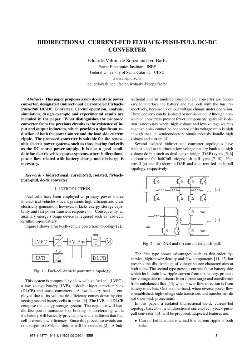
Figure 12 shows voltage and current waveforms of primaryand secondary converter sides when operating at Buckp→s op-eration mode. Channels 1 and 2 refers to vp and vs voltageswhile channels 3 and 4 to ip and is currents. It is possibleto observe that both currents are positive, indicating that thepower comes from primary to secondary side.
11
0306090120
v p(V
)
Vp = 104V
050100150200
v s(V
)
Vs = 163.3V
0481216
i p(A
)
Ip = 9.1A
0 10 20 30 40 50 60
04812
i s(A
)
t (µs)
Is = 5.21A
Fig. 12. : Experimental converter current and voltage wave-forms in Buckp→s operation mode.
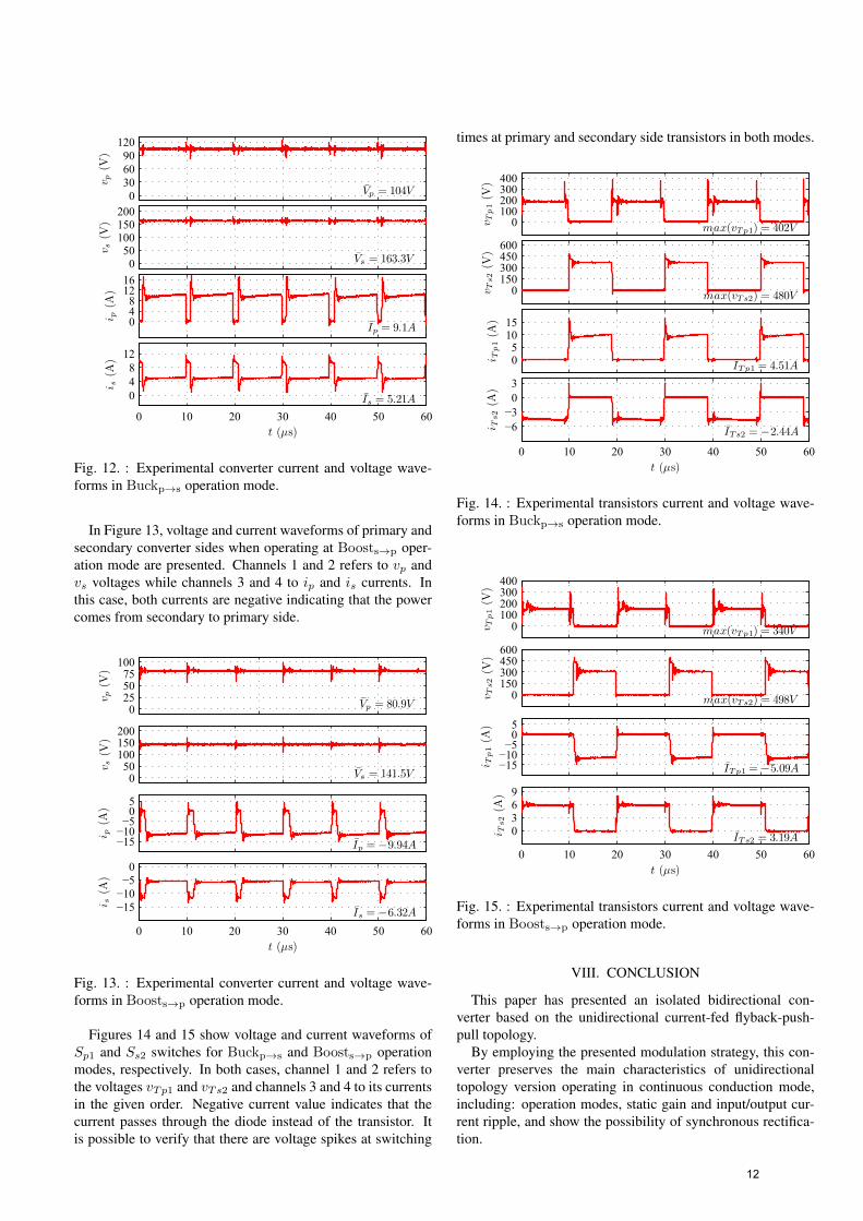
In Figure 13, voltage and current waveforms of primary andsecondary converter sides when operating at Boosts→p oper-ation mode are presented. Channels 1 and 2 refers to vp andvs voltages while channels 3 and 4 to ip and is currents. Inthis case, both currents are negative indicating that the powercomes from secondary to primary side.
0255075100
v p(V
)
Vp = 80.9V
050100150200
v s(V
)
Vs = 141.5V
−15−10−505
i p(A
)
Ip = −9.94A
0 10 20 30 40 50 60
−15−10−50
i s(A
)
t (µs)
Is = −6.32A
Fig. 13. : Experimental converter current and voltage wave-forms in Boosts→p operation mode.
Figures 14 and 15 show voltage and current waveforms ofSp1 and Ss2 switches for Buckp→s and Boosts→p operationmodes, respectively. In both cases, channel 1 and 2 refers tothe voltages vTp1 and vTs2 and channels 3 and 4 to its currentsin the given order. Negative current value indicates that thecurrent passes through the diode instead of the transistor. Itis possible to verify that there are voltage spikes at switching
times at primary and secondary side transistors in both modes.
0100200300400
v Tp1(V
)
max(vTp1) = 402V
0150300450600
v Ts2(V
)
max(vTs2) = 480V
051015
i Tp1(A
)
ITp1 = 4.51A
0 10 20 30 40 50 60
−6−303
i Ts2(A
)
t (µs)
ITs2 = −2.44A
Fig. 14. : Experimental transistors current and voltage wave-forms in Buckp→s operation mode.
0100200300400
v Tp1(V
)
max(vTp1) = 340V
0150300450600
v Ts2(V
)
max(vTs2) = 498V
−15−10−505
i Tp1(A
)
ITp1 = −5.09A
0 10 20 30 40 50 60
0369
i Ts2(A
)
t (µs)
ITs2 = 3.19A
Fig. 15. : Experimental transistors current and voltage wave-forms in Boosts→p operation mode.
VIII. CONCLUSION
This paper has presented an isolated bidirectional con-verter based on the unidirectional current-fed flyback-push-pull topology.
By employing the presented modulation strategy, this con-verter preserves the main characteristics of unidirectionaltopology version operating in continuous conduction mode,including: operation modes, static gain and input/output cur-rent ripple, and show the possibility of synchronous rectifica-tion.
12

Expressions for passive components design were presentedand verified that the flyback primary winding self inductanceis minimized at duty cycle of 50 %.
Experimental results validated the possibility of bi-directional power flow between converter primary and sec-ondary sides and evidenced the necessity of clamping circuitto limit voltage spikes on switches.
REFERENCES
[1] T. Gilchrist, “Fuel cells to the fore [electric vehicles],”IEEE Spectrum, vol. 35, no. 11, pp. 35 –40, Nov. 1998.
[2] J. Bauman and M. Kazerani, “A comparative study offuel-cell–battery, fuel-cell–ultracapacitor, and fuel-cell–battery–ultracapacitor vehicles,” IEEE Transactions onVehicular Technology, vol. 57, no. 2, pp. 760 –769, 2008.
[3] T. Bhattacharya, V. Giri, K. Mathew, and L. Umanand,“Multiphase bidirectional flyback converter topology forhybrid electric vehicles,” IEEE Transactions on Indus-trial Electronics, vol. 56, no. 1, pp. 78 –84, 2009.
[4] J.-S. Lai and D. Nelson, “Energy management powerconverters in hybrid electric and fuel cell vehicles,” Pro-ceedings of the IEEE, vol. 95, no. 4, pp. 766 –777, 2007.
[5] F. Krismer, S. Round, and J. Kolar, “Performance opti-mization of a high current dual active bridge with a wideoperating voltage range,” in Power Electronics Special-ists Conference, 2006. PESC ’06. 37th IEEE, 2006, pp. 1–7.
[6] J. Walter and R. De Doncker, “High-power galvani-cally isolated dc/dc converter topology for future automo-biles,” in Power Electronics Specialist Conference, 2003.PESC ’03. 2003 IEEE 34th Annual, vol. 1, 2003, pp. 27– 32 vol.1.
[7] F. Peng, H. Li, G.-J. Su, and J. Lawler, “A new zvs bidi-rectional dc-dc converter for fuel cell and battery applica-tion,” Power Electronics, IEEE Transactions on, vol. 19,no. 1, pp. 54 – 65, 2004.
[8] S.-J. Jang, T.-W. Lee, W.-C. Lee, and C.-Y. Won, “Bi-directional dc-dc converter for fuel cell generation sys-tem,” in Power Electronics Specialists Conference, 2004.PESC 04. 2004 IEEE 35th Annual, vol. 6, 2004, pp. 4722– 4728 Vol.6.
[9] L. Zhu, “A novel soft-commutating isolated boost full-bridge zvs-pwm dc-dc converter for bidirectional highpower applications,” IEEE Transactions on Power Elec-tronics, vol. 21, no. 2, pp. 422 – 429, 2006.
[10] T. Mishima and E. Hiraki, “Zvs-sr bidirectional dc-dcconverter for supercapacitor-applied automotive electricenergy storage systems,” in 2005 IEEE Conference Vehi-cle Power and Propulsion, 2005, p. 6 pp.
[11] A. Alonso, J. Sebastian, D. Lamar, M. Hernando, andA. Vazquez, “An overall study of a dual active bridgefor bidirectional dc/dc conversion,” in Energy ConversionCongress and Exposition (ECCE), 2010 IEEE, 2010, pp.1129 –1135.
[12] G. Guidi, M. Pavlovsky, A. Kawamura, T. Imakubo, andY. Sasaki, “Efficiency optimization of high power densitydual active bridge dc-dc converter,” in Power Electronics
Conference (IPEC), 2010 International, 2010, pp. 981 –986.
[13] A. I. Pressman, Switching Power Supply Design.McGraw-Hill Professional, 1991.
[14] D. Ruiz-Caballero and I. Barbi, “A new flyback-current-fed push-pull dc-dc converter,” IEEE Transactions onPower Electronics, vol. 14, no. 6, pp. 1056 –1064, Nov.1999.
13