bidirectional isolated full bridge dc –dc …ijesr.org/admin/upload_journal/journal_p---pinki...
TRANSCRIPT

ISSN 2277-2685 IJESR/August 2015/ Vol-5/Issue-8/1107-1118
U. Pinky et.al.,/ International Journal of Engineering & Science Research
*Corresponding Author www.ijesr.org 1107
BIDIRECTIONAL ISOLATED FULL BRIDGE DC –DC CONVERTER WITH
ACTIVE AND PASSIVE SNUBBERS FOR A RENEWABLE ENERGY SYSTEM
U. Pinky*1, K .S .S .Nagateja
2
1M.Tech, Malla Reddy Engineering College (Autonomous), Hyderabad, Telangana, India.
2Asst. Prof, Malla Reddy Engineering College (Autonomous), Hyderabad, Telangana, India.
ABSTRACT
To improve the energy quality, most of the renewable energy systems include an energy storage element
charged by the bidirectional DC-DC converter. This paper proposes the bidirectional isolated full bridge dc –dc
converter with active and passive snubbers for renewable energy system. The low side converter is controlled as
step up and the high side converter is controlled as step down. The proposed framework is portrayed by good
dynamic properties and high efficiency because the converter transistors are switched in ZVS conditions.
Theoretical analyses to provide relations for system design, and the MATLAB/Simulink model investigations to
validate the system characteristic are given in the paper.
Keywords: Bidirectional converter, high conversion ratio, coupled-inductor.
1. INTRODUCTION
In rising oil costs and expanded conditions on remote oil, our vitality approaches have underscored to build the
utilization of renewable vitality, particularly in the territory of sun based vitality assets. This paper depicts the
application grew by using a renewable vitality innovation that sun powered vitality into a solitary or brought
together power era framework. In the majority of the circumstances, sun oriented boards alone are not adequate
to supply the force needs of numerous applications amid the winter months, essentially because of shorter
sunshine time and weaker sun based radiation. Subsequently this sort of vitality is not suitable for discriminating
applications. The proposed innovation tackles this issue by coordinating photovoltaic (PV) power era. Of all
renewable vitality sources, sun based vitality utilizing photovoltaic board is chosen for our venture. The study
was embraced to focus the capacities and to figure out whether the long haul sparing of power .The
improvement of renewable vitality has been an inexorably discriminating point with the developing issue of a
dangerous atmospheric deviation and ecological effects. With an improved examination, elective renewable
sources have turn out to be progressively vital for electric force era.
These options incorporates sunlight based, wind, hydro, geothermal and biomass. They can be delivered today
without harming their capacity to be created later on. Photograph voltaic (PV) is a strategy for changing over
sun oriented vitality into direct current power utilizing semiconducting materials that show the photovoltaic
impact. The most critical part of a sun oriented cell is that it produces sun based vitality straightforwardly to
electrical vitality through the sun powered photovoltaic module. Silicon cells are utilized as a material to
fabricate that voltaic cell. The yield of every cell is moderately low voltage. A sun powered photovoltaic module
is framed by displaying the cells in arrangement.
Block Diagram of Proposed System

U. Pinky et.al.,/ International Journal of Engineering & Science Research
Copyright © 2015 Published by IJESR. All rights reserved 1108
The flyback snubber can reuse the held importance which is orchestrated away in the propping capacitor CC,
while without current encountering the standard switches. It can about lessen the voltage to a fancied respect
just conceivably higher than the voltage over the low side transformer. Since the snubber current does not
course through the fundamental switches, current strain can be diminished essentially under wide weight
condition. Moreover, the flyback snubber can be controlled to precharge the high-side capacitor to keep up a
vital separation from in-surge current amidst a start-up period. In any case, the low- and high-side switches are
worked with hard exchanging side road, perceiving high-voltage spikes.
To handle the as of recently bestowed issue, we first present two fortify capacitors (Cb1 and Cb2) related in
parallel with the upper legs of the voltage-bolstered addition, as showed in Fig. . With these two pad capacitors,
the low- and high-side switches can work with fundamentally zero-voltage exchanging (ZVS) and zero present
exchanging (ZCS). Regardless, when it is worked in attempt down change, these capacitors will resound with
spillage inductance of the transformer, making EMI uproar and making exchanging setback. Besides, two
withdrew capacitor–diode snubbers are proposed to supplement the part flyback snubber, as showed in Fig. .
The proposed snubber arrangement can't just diminish the voltage spike brought on by the present capability
between the spillage inductance and current-kept up inductor streams at any rate, additionally can calm the
downsides of high-present and high-voltage maddens obliged on the standard switches at both turn-on and side
road moves. Also, it can perform close ZVS and ZCS for the switches on both sides of the change.
This attempt can be connected with a photo voltaic centrality change structure at the information side which
converters daylight based significance into force organize in connection of semiconductor benchmarks .This
close to P & O MPPT (most dazzling power point taking after) count to get perfect power extraction.
Fig. 1: Proposed soft-switching bidirectional isolated full-bridge converter with an active flyback and two
passive capacitor–diode snubbers
2. PV SYSTEM
A photovoltaic framework, additionally photovoltaic force framework, sun based PV framework, PV framework
or coolly sun powered cluster, is a force framework intended to supply usable sun oriented power by method for
photovoltaic. It comprises of a plan of a few segments, including sunlight based boards to retain and specifically
change over daylight into power, a sun powered inverter to change the electrical current from DC to AC, and
additionally mounting, cabling and other electrical assistants to set-up a working framework. It might likewise
utilize a sun powered following framework to enhance the framework's general execution or incorporate an
incorporated battery arrangement, as costs for capacity gadgets are required to decrease. Entirely talking, a
sunlight based cluster just incorporates the group of sun powered boards, the unmistakable piece of the PV
framework, and does exclude the various equipment, frequently compressed as offset of framework (BOS). In
addition, PV frameworks change over light straightforwardly into power and shouldn't be mistaken for other sun
based advancements, for example, concentrated sun powered force (CSP) and sun oriented warm, utilized for
both warming and cooling.

U. Pinky et.al.,/ International Journal of Engineering & Science Research
Copyright © 2015 Published by IJESR. All rights reserved 1109
2.1 Solar Panel
Sunlight based boards are gadgets that change over light into power. They are called "sunlight based" boards
and light power due to the effective accessibility of sun's radiation as both warmth and light .Photo voltaic
innovation characterization into silicon crystalline innovation and slight film innovation. In this proposed
system silicon crystalline is utilized. The crystalline silicon PV cell is one of numerous silicon-based
semiconductor gadgets.
2.2 Maximum Power Point Tracking
Most extreme force point following (MPPT) is a strategy in which framework associated inverters, battery
chargers and related gadgets are utilized to get greatest conceivable force from single or more voltaic modules.
Photovoltaic sunlight based cells have a mind boggling relationship between sun powered irradiance,
temperature and aggregate resistance that delivers a non-direct yield effectiveness which can be investigated in
light of the i-v bend. The motivation behind the MPPT framework is to test the PV cell's yield and to apply the
best possible resistance (burden) to get most extreme force at any given states of a situation. Transformation,
sifting, and regulation of voltage or current for driving different burdens are given by MPPT gadgets which are
normally incorporated into an electric force converter system.the change of the dc energy to air conditioning
force should be possible by sun oriented inverters and may join MPPT. Such inverters test the yield power (i-v
bend) from the sun powered modules and apply the best possible resistance (load) to get most extreme force.
The result of the mppvoltage(Vmpp) and mpp current(Impp) will give mpp-most extreme force point esteem.
The most extreme force point tracker (MPPT) is expected to streamline the measure of force acquired from the
photovoltaic cluster to the force supply.
Fig. 2: I-V curve
The yield of a sunlight based module is portrayed by an execution bend of voltage versus present, called the i-v
bend. The greatest force purpose of a sunlight based module is the point along the i-v bend that compares to the
most extreme yield power workable for the module. Discovering the most extreme region under the current
versus voltage bend gives bend esteem.
The yield of a sun based module is portrayed by an execution bend of voltage versus present, called the i-v
bend. The most extreme force purpose of a sun oriented module is the point along the iv bend that compares to
the greatest yield power feasible for the module. Discovering the greatest range under the current versus voltage
bend gives bend value.
3. TOPOLOGY, CONTROL PRINCIPLE AND MODES OF OPERATIONS
The proposed delicate exchanging bidirectional secluded full extension converter with a dynamic flyback and
two aloof capacitor–diode snubbers is demonstrated in Fig. 4. It can be worked with two sorts of
transformations: venture up transformation and venture down change. Fig. comprises of a current-nourished
switch connect, a dynamic flyback snubber at the low-voltage side, a voltage-sustained switch scaffold, and a
uninvolved snubber pair at the high-voltage side. Inductor Lm performs yield sifting when force stream from the
high-voltage side to the low-voltage side, which is indicated as a stage down change. Then again, it meets
expectations in the progression up transformation. In addition, snubber capacitor CC and diode DC are utilized
to retain the present contrast between current-encouraged inductor current iL and spillage inductance current iP
of detachment transformer TP amid exchanging compensation.

U. Pinky et.al.,/ International Journal of Engineering & Science Research
Copyright © 2015 Published by IJESR. All rights reserved 1110
The flyback snubber is worked to exchange the vitality put away in snubber capacitor CC to support capacitors
Cb1 and Cb2, and voltage VC can drop to zero. In this way, the voltage anxieties of switches M1 ~ M4 can be
constrained to a lower level, accomplishing close ZCS side road. The fundamental benefits of the proposed
snubber incorporate no spike current flowing through the switches and accomplishing delicate exchanging
elements. Note that high spike current can bring about charge relocation, over current thickness, and additional
attractive power which will disintegrate in MOSFET transporter thickness, channel width, and wire holding and,
thusly, build its conduction resistance.
In the progression up change, switchesM1 ~ M4 are controlled, and the body diodes of switches M5 ~ M8 serve
as a rectifier. In the progression down transformation, switches M5 ~ M8 are controlled, and the body diodes of
switches M1 ~ M4 work as a full-connect rectifier. To rearrange the relentless state examination, a few
suppositions are made as takes after.
1) All parts are perfect aside from that the transformer is connected with spillage inductance.
2) Inductor Lm is sufficiently huge to keep the current IL steady more than an exchanging period.
3) Snubber capacitor CC is much bigger than the parasitic capacitance of switches M1 ∼ M8.
A. Step Up Conversion
In the progression up change, switches M1 ~ M4 are worked like a help converter, where switch sets (M1, M2)
and (M3, M4) behavior to store vitality in Lm. At the high-voltage side, body diodes D5 ~ D8 of switchesM5 ~
M8 will direct to exchange energy to CHV. At the point when switch sets (M1, M2) and (M3, M4) are changed
to (M1, M4) or (M2, M3), current distinction iC (= iL − iP) will charge capacitor CC until iP ascends to iL, and
capacitor voltage VC will be cinched to VHV • (NP/NS), accomplishing close ZCS side road for M2 or M4.
Meanwhile, high-side current iS has the need moving through one of the two uninvolved capacitor–diode
snubbers, and either Cb1 or Cb2 will be completely released before diode D5 or D7 conducts. At the point when
switch pair (M1,M4) or (M2,M3) is changed back to (M1,M2) and (M3,M4), switch M2 or M4 can have close
ZCS turn-on highlight because of spillage inductance Lll restricting the di/dt of high-side diode-reverse-
recuperation current. The flyback snubber works at the same time to release snubber capacitor CC and exchange
the put away vitality to support capacitors Cb1 and Cb2. With the flyback snubber, the vitality assimilated in CC
won't move through switches M1 ~ M4, which can decrease their present hassles drastically when the spillage
inductance of the separation transformer is noteworthy.
The key voltage and current waveforms of the converter worked in the progression up transformation are
indicated in Fig.2. An itemized portrayal of the converter operation more than a half exchanging cycle is
exhibited as takes after.
Mode 1 [t0 ≤ t < t1]:
Before t0, the greater part of the four switches M1 ~ M4 are turned on. Inductor Lm is charged by VLV. At t0,
M1 and M4 stay directing, while M2 and M3 are killed. At that point, clipping diode DC conducts, and snubber
capacitor CC is charged by the present distinction iC. In this mode, the flyback snubber still stays in the OFF
state. The comparable circuit is indicated in Fig. 4(a).
Mode 2 [t1 ≤ t < t2]:
In this mode, spillage inductance current iP will begin to track current iL, and cradle capacitor Cb1 will begin to
discharge vitality. At time t2, current iP is equivalent to current iL, the voltage of switches M2 and M3 and
capacitor CC will achieve the most extreme esteem all the while, and its equal circuit is demonstrated in Fig. 4
(b) A close ZCS delicate exchanging is along these lines achieved amid t0 to t2.
Mode 3 [t2 ≤ t < t3]:
Before t3, the vitality put away in cushion capacitor Cb1 is not completely released yet. Hence, the capacitor
won't quit releasing until Vb1 drops to zero. The comparable circuit is demonstrated in Fig. 4(c).

U. Pinky et.al.,/ International Journal of Engineering & Science Research
Copyright © 2015 Published by IJESR. All rights reserved 1111
Mode 4 [t3 ≤ t < t4]:
At the point when the vitality put away in Cb1 has been totally discharged to the yield at t3, diode D5 will lead.
The circuit operation over this time interim is indistinguishable to a general side road condition of a traditional
current-encouraged full-connect converter. The identical circuit is demonstrated in Fig. 4(d).
Mode 5 [t4 ≤ t < t5]:
At t4, the majority of the four switches M1 ~ M4 are turned on once more, and switch MS of the flyback
snubber is turned on synchronously. SwitchesM2 andM3 accomplish a ZCS turn-on delicate changing element
because of Lll, and current iP drops to zero steadily. In the flyback snubber, the vitality put away in capacitor
CC will be conveyed to the polarizing inductance of transformer TS. The proportionate circuit is demonstrated
in Fig. 4(e).
Mode 6 [t5 ≤ t < t6]:
At the point when switch MS is killed at t5, capacitor voltage VC drops to zero, and the vitality put away in the
polarizing inductance will be exchanged to cushion capacitor Cb1. In this mode, the time interim of driving sign
Vgs(Ms) is marginally more than the releasing time of capacitor CC. The reason for existing is to guarantee that
the vitality put away in capacitor CC can be totally discharged, making a ZCS operational open door for switch
M2 or M4 at the following side road move. The equal circuit is demonstrated in Fig. 4(f).
Fig. 3: Key voltage and current waveforms of the proposed converter operated in the step-up conversion

U. Pinky et.al.,/ International Journal of Engineering & Science Research
Copyright © 2015 Published by IJESR. All rights reserved 1112
Mode 7 [t6 ≤ t < t7]:
At t6, the vitality put away in the polarizing inductance of transformer TS was totally exchanged to cradle
capacitor Cb1, and the circuit operation is indistinguishable to a normal turn-on condition of an ordinary
Fig. 4: Operation modes of the step-up conversion (a) Mode 1 (b) Mode 2# (c) Mode 3 (d) Mode 4 (e)
Mode 5 (f) Mode 6 (g) Mode 7

U. Pinky et.al.,/ International Journal of Engineering & Science Research
Copyright © 2015 Published by IJESR. All rights reserved 1113
current-sustained converter. Its proportionate circuit is indicated in Fig. 4(g). The circuit operation stops at t7
and finishes a half-exchanging cycle.
Fig. 5: Key voltage and current waveforms of the proposed converter operated in the step-down
conversion
B. Step-Down Conversion
In the examination, the spillage inductance of the transformer at the low-voltage side is reflected to the high-
voltage side in which proportionate inductance L*eq levels with (Llh + Lll • N2s/N2p).
In the movement down change, switches M5 ∼ M8 are worked like a buck converter in which switch sets (M5,
M8) and (M6, M7) substitute guiding to trade power from capacitor CHV to battery BLV. For lessening spillage
inductance affect on voltage spike, switches M5 ~ M8 are worked with stage development control, achieving
ZVS turn-on parts. Yet there is no convincing motivation to hold the present difference amidst iL and iP ,
capacitor CC can help snap the voltage ringing in light of L*eq and the parasitic capacitance of M1 ∼ M4. With
the two detached capacitor–diode snubbers, switches M6 and M8 can achieve close ZCS side street.
The key voltage and current waveforms of the converter worked in the movement down change are shown in
Fig. 7. An unmistakable depiction of its operation more than a half-trading cycle is displayed as takes after.
Mode 1 [t0 ≤ t < t1]:
In this mode, switchesM5 andM8 are turned on, whileM6 andM7 are in the OFF state. The high-side voltage
VHV is crossing the transformer, and it is, to be perfectly honest, crossing the equivalent inductance L*eq and
drives current iS to climb with the inclination of VHV/L*eq. With the transformer current extending toward the
load current level at t1, the body diodes (D1 and D4) are prompting trade power and the voltage over the
transformer terminals on the low-voltage side changes right away to reflect the voltage from the high-voltage
side. The equivalent circuit is shown in Fig.6(a)
Mode 2 [t1 ≤ t < t2]:
At t1, switchM8 stays driving, while M5 is slaughtered. The body diode of M6 then starts coordinating the
freewheeling spillage current. The transformer current iS accomplishes the load current level at t1, and VAB
rises to the reflected voltage (VHV • NP/NS). Cutting diode DC starts driving the full current of L*eq and the
parasitic capacitance ofM1 ∼ M4. In the meantime, switch MS of the flyback snubber is turned on and starts
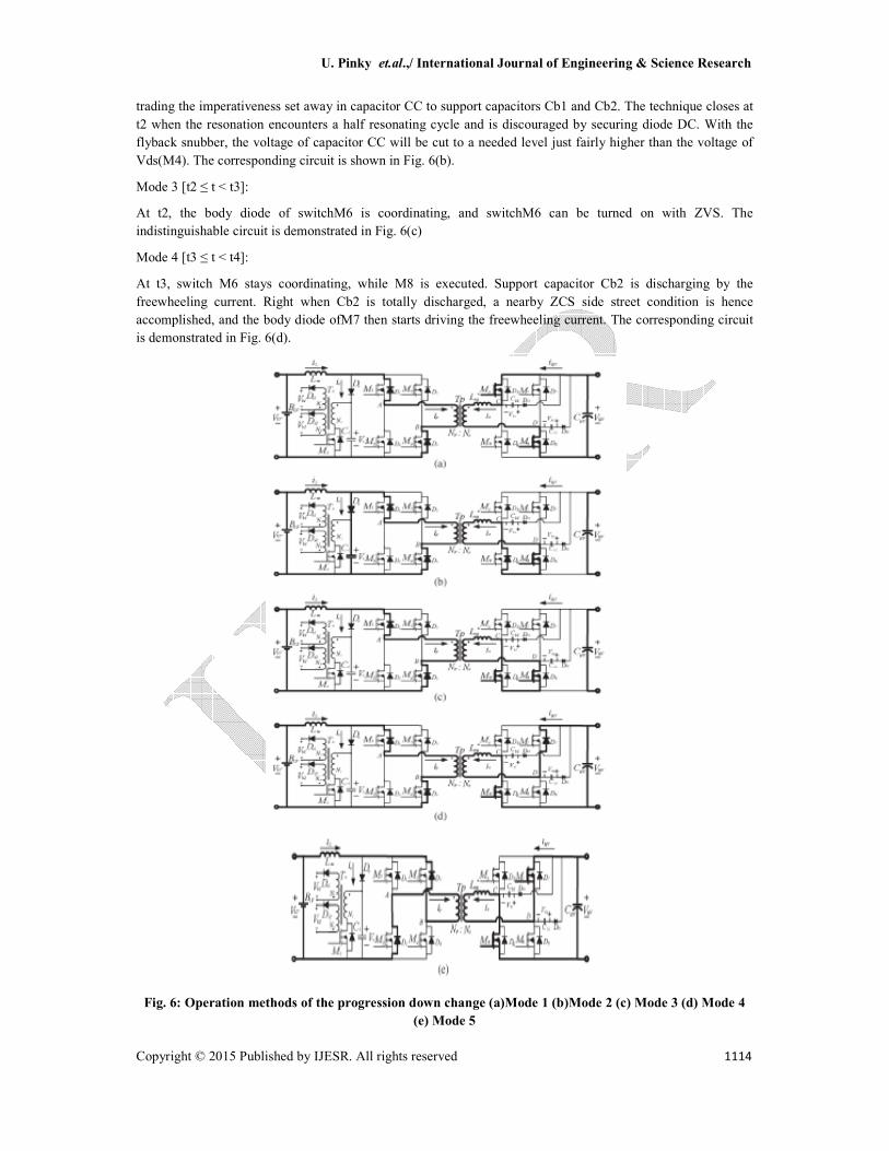
U. Pinky et.al.,/ International Journal of Engineering & Science Research
Copyright © 2015 Published by IJESR. All rights reserved 1114
trading the imperativeness set away in capacitor CC to support capacitors Cb1 and Cb2. The technique closes at
t2 when the resonation encounters a half resonating cycle and is discouraged by securing diode DC. With the
flyback snubber, the voltage of capacitor CC will be cut to a needed level just fairly higher than the voltage of
Vds(M4). The corresponding circuit is shown in Fig. 6(b).
Mode 3 [t2 ≤ t < t3]:
At t2, the body diode of switchM6 is coordinating, and switchM6 can be turned on with ZVS. The
indistinguishable circuit is demonstrated in Fig. 6(c)
Mode 4 [t3 ≤ t < t4]:
At t3, switch M6 stays coordinating, while M8 is executed. Support capacitor Cb2 is discharging by the
freewheeling current. Right when Cb2 is totally discharged, a nearby ZCS side street condition is hence
accomplished, and the body diode ofM7 then starts driving the freewheeling current. The corresponding circuit
is demonstrated in Fig. 6(d).
Fig. 6: Operation methods of the progression down change (a)Mode 1 (b)Mode 2 (c) Mode 3 (d) Mode 4
(e) Mode 5

U. Pinky et.al.,/ International Journal of Engineering & Science Research
Copyright © 2015 Published by IJESR. All rights reserved 1115
Mode 5 [t4 ≤ t < t5]:
At t4, with the body diode of switch M7 coordinating, M7 can be turned on with ZVS. Over this time interval,
the dynamic changes change to the following pair of switches, and the voltage over the transformer pivots its
furthest point. The circuit operation stops at t5 and completions a half-trading cycle. The relative circuit is
shown in Fig. 6(e).
4. SIMULATION RESULTS
Simulation is performed using MATLAB/SIMULINK software. Simulink liabrary files include inbuilt models
of many electrical and electronics components and devices such as diodes, MOSFETS, capacitors, power
supplies and so on. The circuit components are connected as per design without error, parameters of all
components are configured as per requirement and simulation is performed.
Six 36-cell strings
‘Si’ material
Array Open Circuit voltage=50V
Array Short Circuit current =7.34A
Wattage=369W
Operating Temp=25.1C
Radiation=1000W/m2
Source side inductance Lm=500uH
Capacitance Cc=100nF
Diode ratings:
R_ON=0.001 Ohm
Vfd=0.8V
Snubber: Rs=500 Ohm; Cs=250nF
Flyback transformer ratings:
100VA 50Hz
n=1/ 4.25
Winding-1: R=4.3 Ohm, L1=0.4H
Windinf-2: R=0.793 Ohm, L2=0.08H
Rm=1Mohm; Lm=2866H
Active snubber prameters:
Li=500uH
Cc=100nF
Three Winding Transformer
100VA, 50Hz
Winding-1 : 50V, R1=4.3 Ohm, L1=0.45H
Winding-2: 150V, R2=0.793 Ohm, L2=0.084H
Winding-3: 150V, R3=0.793 Ohm, L3=0.084H

U. Pinky et.al.,/ International Journal of Engineering & Science Research
Copyright © 2015 Published by IJESR. All rights reserved 1116
Turns ration , n=1:3
Simulation Circuit
PV Boost Converter
PV Cell Model

U. Pinky et.al.,/ International Journal of Engineering & Science Research
Copyright © 2015 Published by IJESR. All rights reserved 1117
Waveforms
a) Input voltage
b) Output voltage
Calculations
Input voltage from PV=800V
Output voltage at HV side =1700V
Therefore, conversion ratio M= Vo/Vin
=1700/800
=2.1
5. CONCLUSION
Thus a bidirectional isolated full bridge dc –dc converter with active and passive snubbers for renewable energy
system like PV system is employed here. This converter is designed for high voltage gain so that the low dc
voltage from PV is stepped up to suitable ratio. This is studied using MATLAB/ SIMULINK study
REFERENCES
[1] Zhang Z, Thomsen OC, Andersen MAE. Optimal design of a push–pull–forward half-bridge (PPFHB)
bidirectional DC–DC converter with variable input voltage. IEEE Trans. Ind. Electron 2012; 59(7): 2761–2771.
[2] Ghodke DV, Chatterjee K, Fernandes BG. Modified soft switched three-phase three-level DC–DC converter
for high-power applications having extended duty cycle range. IEEE Trans. Ind. Electron 2012; 59(9): 3362–
3372.
[3] Zhang F, Xiao L, Yan Y. Bi-directional forward-flyback DC–DC converter. Proc. IEEE Power Electron.
Spec. Conf 2004; 5: 4058–4061.
[4] Li H, Liu D, Peng FZ, Su GJ. Small signal analysis of a dual half bridge isolated ZVS bi-directional DC–DC
converter for electrical vehicle applications. Proc. IEEE Power Electron. Spec. Conf 2005; 2777–2782.
[5] Yang LS, Liang TJ. Analysis and implementation of a novel bidirectional DC–DC converter. IEEE Trans.
Ind. Electron 2012; 59(1): 422–434.
[6] Liu D, Li H. Design and implementation of a DSP based digital controller for a dual half bridge isolated bi-
directional DC–DC converter. Proc. IEEE Appl. Power Electron. Conf 2006; 695–699.

U. Pinky et.al.,/ International Journal of Engineering & Science Research
Copyright © 2015 Published by IJESR. All rights reserved 1118
[7] Zhao B, Yu Q, Leng Z, Chen X. Switched Z-source isolated bidirectional DC–DC converter and its phase-
shifting shoot-through bivariate coordinated control strategy. IEEE Trans. Ind. Electron 2012; 59(12): 4657–
4670.
[8] Madawala UK, Neath M, Thrimawithana DJ. A power-frequency controller for bidirectional inductive
power transfer systems. IEEE Trans. Ind. Electron 2013; 60(1): 310–317.
[9] Aggeler D, Biela J, Inoue S, Akagi H, Kolar JW. Bi-directional isolated DC–DC converter for next-
generation power distribution comparison of converters using Si and SiC devices. Proc. Power Convers. Conf.,
2007; 510–517.
[10] Krishnaswami H, Mohan N. A current-fed three-port bidirectional DC–DC converter. Proc. Telecommun.
Energy Conf.2007; 523–526.
[11] Garcia O, Flores LA, Oliver JA, Cobos JA, De la Pena J. Bidirectional DC–DC converter for hybrid
vehicles. Proc. IEEE Power Electron. Spec. Conf 2005; 1881–1886.
[12] Yujin S, Enjeti PN. A new soft switching technique for bidirectional power flow, full-bridge DC–DC
converter. Conf. Rec. IEEE IAS Annu. Meeting 2002; 4: 2314–2319.
[13] Wang K, Lin CY, Zhu L, Qu D, Lee FC, Lai JS. Bi-directional DC–DC converters for fuel cell systems.
Proc. IEEE Power Electron. Transp 1998; 47–51.
[14] Zhu L. A novel soft-commutating isolated boost full-bridge ZVS-PWM DC–DC converter for bidirectional
high power applications. IEEE Trans. Power Electron 2006; 21(2): 422–429.
[15] Thrimawithana DJ, Madawala UK, Neath M. A synchronization technique for bidirectional IPT systems.
IEEE Trans. Ind. Electron 2013; 60(1): 301–309.
[16] Chen W, Rong P, Lu Z. Snubberless bidirectional DC–DC converter with new CLLC resonant tank
featuring minimized switching loss. IEEE Trans. Ind. Electron 2010; 57(9): 3075–3086.
[17] Ma G, Qu W, Yu G, Liu Y, Liang N, Li W. A zero-voltageswitching bidirectional DC–DC converter with
state analysis and softswitching-oriented design consideration. IEEE Trans. Ind. Electron 2009; 56(6): 2174–
2184.
[18] Wu TF, Chen YC, Yang JG, Kuo CL. Isolated bidirectional full-bridge DC–DC converter with a flyback
snubber. IEEE Trans. Power Electron 2010; 25(7): 1915–1922.
[19] Mousavi A, Das P, Moschopoulos G. A comparative study of a new ZCS DC–DC full-bridge boost
converter with a ZVS active-clamp converter. IEEE Trans. Power Electron 2011; 27(3): 1347–1358.