bipolar n-p-n transistors level 503 - nxp.com · the n channel mextram 503 model and the n channel...
TRANSCRIPT

December 2009 Bipolar N-P-N Transistors Level 503
1 Bipolar N-P-N Transistors Level 503
© NXP 1992-2009 1TOC Index Quitfile
ttt
t

Bipolar N-P-N Transistors Level 503 December 2009
1.1 Introduction
In this chapter the Mextram 503 models are described as the n channel model and the n chan-nel substrate model. The models provide a detailed description of a vertical integrated circuit NPN transistor. It is meant to be used for DC, transient and AC analyses at all current levels, i.e. high and low injection, quasi and hard saturation. In comparison with the n channel Mex-tram 502 model, the description of the collector region is improved. The base-collector depletion charge and the reverse current now depend on the same internal base-collector
voltage . The modeling of the epilayer resistance is rewritten and takes into account
current spreading. All this results in a more accurate modeling of the collector transit time. Other parts of the models are rewritten to obtain better convergency behaviour. For Pstar and Spectre users they are available as built-in model.
The n channel Mextram 503 model and the n channel substrate Mextram 503 model are almost identical. In case of a difference between the models, it is mentioned explicitly that the information given is only relevant for the n channel Mextram 503 model or the n channel substrate Mextram 503 model.
1.2 Simulator specific items
1.2.1 Pstar syntax
n channel model : tn_n (c, b, e) level=503, <parameters> n channel substrate model : tns_n (c, b, e, s) level=503, <parameters> n : occurrence indicator <parameters> : list of model parameters c, b, e and s are collector, base, emitter and substrate terminals respectively.
I R
V B2C2
2 © NXP 1992-2009 TOC Index Quitfile
ttt
t

December 2009 Bipolar N-P-N Transistors Level 503
1.2.2 Spectre syntax
n channel model :model modelname bjt503 type=npn1 <modpar> componentname c b e modelname <inpar>
n channel substrate model :model modelname bjt503 type=npn1 <modpar> componentname c b e s modelname <inpar>
modelname : name of model, user defined componentname : occurrence indicator
<modpar> : list of model parameters2
<inpar> : list of instance parameters1
c, b, e and s are collector, base, emitter and substrate terminals respectively.
Note3The n-channel model has a substrate node that is implicitly connected to ground. To describe a real 3-terminal device for Spectre, put iss=0 and cjs=0.
1.Either pnp or pnpl are interpreted as lateral pnp.2.For more details of these Spectre parameters see also Cadence Spectre Circuit Simulator Reference, version 4.4.6 or 5.0.
© NXP 1992-2009 3TOC Index Quitfile
ttt
t

Bipolar N-P-N Transistors Level 503 December 2009
1.3 Survey of modeled effects
• Temperature effects
• Charge storage effects
• Substrate effects and parasitic pnp (for the TNS device only)
• High-injection effects
• Built-in electric field in base region
• Bias-dependent Early effect
• Low-level non-ideal base currents
• Hard and quasi-saturation
• Weak avalanche
• Hot carrier effects in the collector epilayer
• Explicit modeling of inactive regions
• Split base-collector depletion capacitance
• Current crowding and conductivity modulation for base resistance
• First order approximation of distributed high frequency effects in the intrinsic base (high frequency current crowding and excess phase shift).
4 © NXP 1992-2009 TOC Index Quitfile
ttt
t

December 2009 Bipolar N-P-N Transistors Level 503
1.4 Parameters
The parameters for TN-level-503 and TNS-level-503 are listed in the table below. .
Position Parameter Units Description
in list name
TN TNS
1 1 LEVEL - Model level, must be set to 503
2 2 MULT - Multiplication factor
3 3 TREF °C Reference temperature
4 4 DTA K Difference of the device temperature to the ambi-ent temperature
5 5 EXMOD - Flag for extended modeling of the reverse current gain (default is .false. =0 and .true. =1)
6 6 EXPHI - Flag for distributed high frequency effects in tran-sient (default is .false. =0 and .true. =1)
7 7 EXAVL - Flag for extended modeling of avalanche currents (default is .false =0 and .true. =1)
8 8 IS A Collector-emitter saturation current
9 9 BF - Ideal forward current gain
10 10 XIBI - Fraction of ideal base current that belongs to the sidewall
11 11 IBF A Saturation current of the non-ideal forward base current
12 12 VLF V Cross-over voltage of the non-ideal forward base current
13 13 IK A High-injection knee current
14 14 BRI - Ideal reverse current gain
15 15 IBR A Saturation current of the non-ideal reverse base current
16 16 VLR V Cross-over voltage of the non-ideal reverse base current
17 17 XEXT - Part of IEX, QEX, QTEX and ISUB that depends on the base-collector voltage VBC1
18 18 QBO C Base charge at zero bias
T DEVICE T AMBIENT DTA+=( )
© NXP 1992-2009 5TOC Index Quitfile
ttt
t

Bipolar N-P-N Transistors Level 503 December 2009
19 19 ETA - Factor of the built-in field of the base
20 20 AVL - Weak avalanche parameter
21 21 EFI - Electric field intercept (with EXAVL=1).
22 22 IHC A Critical current for hot carriers
23 23 RCC Ω Constant part of the collector resistance
24 24 RCV Ω Resistance of the unmodulated epilayer
25 25 SCRCV Ω Space charge resistance of the epilayer
26 26 SFH - Current spreading factor epilayer
27 27 RBC Ω Constant part of the base resistance
28 28 RBV Ω Variable part of the base resistance at zero bias
29 29 RE Ω Emitter series resistance
30 30 TAUNE s Minimum delay time of neutral and emitter charge
31 31 MTAU - Non-ideality factor of the neutral and emitter charge
32 32 CJE F Zero bias collector-base depletion capacitance
33 33 VDE V Emitter-base diffusion voltage
34 34 PE - Emitter-base grading coefficient
35 35 XCJE - fraction of the emitter-base depletion capacitance that belongs to the sidewall
36 36 CJC F Zero bias collector-base depletion capacitance
37 37 VDC V Collector-base diffusion voltage
38 38 PC - Collector-base grading coefficient variable part
39 39 XP - Constant part of of CJC
40 40 MC - Collector current modulation coefficient
41 41 XCJC - fraction of the collector-base depletion capaci-tance under the emitter area
42 42 VGE V Band-gap voltage of the emitter
43 43 VGB V Band-gap voltage of the base
44 44 VGC V Band-gap voltage of the collector
45 45 VGJ V Band-gap voltage recombination emitter-base junction
Position Parameter Units Description
in list name
TN TNS
η=( )
6 © NXP 1992-2009 TOC Index Quitfile
ttt
t

December 2009 Bipolar N-P-N Transistors Level 503
Note3The parameters marked by * are not valid for the TN-level-503 model.
46 46 VI V Ionization voltage base dope
47 47 NA cm-3 Maximum base dope concentration
48 48 ER - Temperature coefficient of VLF and VLR
49 49 AB - Temperature coefficient resistivity base
50 50 AEPI - Temperature coefficient resistivity of the epilayer
51 51 AEX - Temperature coefficient resistivity of the extrinsic base
52 52 AC - Temperature coefficient. restivity of the buried layer
53 53 KF - Flickernoise coefficient ideal base current
54 54 KFN - Flickernoise coefficient non-ideal base current
55 55 AF - Flickernoise exponent
* 56 ISS A base-substrate saturation current
* 57 IKS A Knee current of the substrate
* 58 CJS F Zero bias collector-substrate depletion capacitance
* 59 VDS V Collector-substrate diffusion voltage
* 60 PS - Collector-substrate grading coefficient
* 61 VGS V Band-gap voltage of the substrate
* 62 AS - For a closed buried layer: AS=AC For an open buried layer: AS=AEPI
Position Parameter Units Description
in list name
TN TNS
© NXP 1992-2009 7TOC Index Quitfile
ttt
t

Bipolar N-P-N Transistors Level 503 December 2009
Parameter MULT
This parameter may be used to put several transistors in parallel. To scale the geometry of a transistor use of the process-block is preferable over using this feature. The following parameters are multiplied by MULT:
Divided by MULT are:
The TN device: IS IK IBF IBR QBO IHC CJE CJC
The TNS device: IS IK IBF IBR ISS IKS QBO IHC CJE CJC CJS
RCC SCRCV RCV RBC RBV RE
8 © NXP 1992-2009 TOC Index Quitfile
ttt
t

December 2009 Bipolar N-P-N Transistors Level 503
Default and clipping values
The default values and clipping valuesfor the TN/TNS-level-503 are listed below (The parameters marked by * are not valid for the TN-level-503 model).
No. Parameter Units Default Clip low Clip high
1 LEVEL - 503 - -
2 MULT - 1.00 0.0 -
3 TREF °C 25.00 -273.15 -
4 DTA K 0.00 - -
5 EXMOD - 1.00 0.0 1.0
6 EXPHI - 0.00 0.0 1.0
7 EXAVL - 0.00 0.0 1.0
8 IS A 5.00 ×10⁻¹⁷ 0.0 -
9 BF - 140.00 1.0 ×10⁻⁴ -
10 XIBI - 0.00 0.0 1.0
11 IBF A 2.00 ×10⁻¹⁴ 0.0 -
12 VLF V 0.50 - -
13 IK A 15.00 ×10⁻³ 1.0 ×10⁻¹² -
14 BRI - 16.00 1.0 ×10⁻⁴ -
15 IBR A 8.00 ×10⁻¹⁵ 0.0 -
16 VLR V 0.50 - -
17 XEXT - 0.50 0.0 1.0
18 QBO C 1.20 ×10⁻¹² 1.0 ×10⁻¹⁸ -
19 ETA - 4.00 0.0 -
20 AVL - 50.00 0.1 -
21 EFI - 0.70 0.0 -
22 IHC A 3.00 ×10⁻³ 1.0 ×10⁻¹² -
23 RCC Ω 25.00 1.0 ×10⁻⁶ -
24 RCV Ω 750.00 1.0 ×10⁻⁶ -
25 SCRCV Ω 1000.00 1.0 ×10⁻⁶ -
© NXP 1992-2009 9TOC Index Quitfile
ttt
t

Bipolar N-P-N Transistors Level 503 December 2009
26 SFH - 0.60 0.0 -
27 RBC Ω 50.00 1.0 ×10⁻⁶ -
28 RBV Ω 100.00 1.0 ×10⁻⁶ -
29 RE Ω 2.00 1.0 ×10⁻⁶ -
30 TAUNE s 3.00 ×10⁻¹⁰ 0.0 -
31 MTAU - 1.18 1.0 2.0
32 CJE F 2.50 ×10⁻¹³ 1.0 ×10⁻²¹ -
33 VDE V 0.90 0.05 -
34 PE - 0.33 0.01 0.99
35 XCJE - 0.50 0.0 1.0
36 CJC F 1.30 ×10⁻¹³ 1.0 ×10⁻²¹ -
37 VDC V 0.60 0.05 -
38 PC - 0.40 0.01 0.99
39 XP - 0.20 0.0 1.0
40 MC - 0.50 0.0 1.0
41 XCJC - 0.10 0.0 0.999
42 VGE V 1.01 0.1 -
43 VGB V 1.18 0.1 -
44 VGC V 1.205 0.1 -
45 VGJ V 1.10 0.1 -
46 VI V 0.04 0.0 -
47 NA cm-3 3.00 ×10¹⁷ 1.0 ×10² -
48 ER - 2.00 ×10⁻³ - -
49 AB - 1.35 - -
50 AEPI - 2.15 - -
51 AEX - 1.00 - -
52 AC - 0.40 - -
53 KF - 2.00 ×10⁻¹⁶ 0.0 -
54 KFN - 2.00 ×10⁻¹⁶ 0.0 -
No. Parameter Units Default Clip low Clip high
10 © NXP 1992-2009 TOC Index Quitfile
ttt
t

December 2009 Bipolar N-P-N Transistors Level 503
55 AF - 1.00 0.01 -
56* ISS A 6.00 ×10⁻¹⁶ 0.0 -
57* IKS A 5.00 ×10⁻⁶ 1.0 ×10⁻¹² -
58* CJS F 1.00 ×10⁻¹² 0.0 -
59* VDS V 0.50 0.05 -
60* PS - 0.33 0.01 0.99
61* VGS V 1.15 0.1 -
62* AS - 2.15 - -
No. Parameter Units Default Clip low Clip high
© NXP 1992-2009 11TOC Index Quitfile
ttt
t

Bipolar N-P-N Transistors Level 503 December 2009
1.5 Pstar specific items
1.5.1 The ON/OFF condition
The solution of a circuit involves a process of successive calculations. The calculations are started from a set of ‘initial guesses’ for the electrical quantities of the nonlinear elements. A simplified DCAPPROX mechanism for devices using ON/OFF keywords is mentioned in [56]. By default the devices start in the default state.
TN level 503 TNS level 503
Default ON OFF Default ON OFF
VBC1 -1.0 0.0 -1.0 VBC1 -1.0 0.0 -1.0
VB1C1 -1.0 0.0 -1.0 VB1C1 -1.0 0.0 -1.0
VB2C1 -1.0 0.0 -1.0 VB2C1 -1.0 0.0 -1.0
VB2C2 -1.0 0.0 -1.0 VB2C2 -1.0 0.0 -1.0
VB1E1 0.65 0.75 -0.3 VB1E1 0.65 0.75 -0.3
VB2E1 0.65 0.75 -0.3 VB2E1 0.65 0.75 -0.3
VB1B2 1.0 ×10⁻⁶ 1.0 ×10⁻⁶ 0.0 VB1B2 1.0 ×10⁻⁶ 1.0 ×10⁻⁶ 0.0
VSC1 -5.0 -5.0 -5.0
12 © NXP 1992-2009 TOC Index Quitfile
ttt
t

December 2009 Bipolar N-P-N Transistors Level 503
1.5.2 Numerical Adaptation
To implement the model in a circuit simulator, care must be taken of the numerical stability of the simulation program. A small non-physical conductance, Gmin, is connected between
the nodes B1C1 and B2E1. The value of the conductance is 10-13 [1/Ω].
1.5.3 DC operating point output
The DC operating point output facility gives information on the state of a device at its opera-tion point.
For the TNS device:
Quantity Equation Description
LEVEL 503 Model level
RE RE Emitter resistance
RCC RCC Constant part of the collector resistance
RBC RBC Constant part of the base resistance
RBV rbv Variable part of the base resistance:
GPI Conductance floor b-e junction:
SGPI Conductance sidewall b-e junction:
dI n gx dV B2E1 g y dV B2C2 gz dV B2C1⋅+⋅+⋅=
dI C1C2 grcvy dV B2C2 grcvz dV B2C1⋅+⋅=
dI BE jω Cbey dV B2C2 Cbez dV B2C1⋅+⋅( )⋅=
dI BC gµx dV B2E1 gµz dV B2C1 jω Cbcx dV B2E1 Cbcz dV B2C1⋅+⋅( )⋅+⋅+⋅=
dI B1B2 grbvx dV B2E1 grbvy dV B2C2 grbvz dV B2C1⋅ jω CB1B2xdV B2E1⋅ ⋅+ +⋅+⋅=
dSI BE jω SCTE dV B2E1⋅ ⋅=
dI SUB gPNP dV B1C1 XgPNP dV BC1⋅+⋅=
1 ∂I B1B2 ∂V B1B2⁄( )⁄
gπ∂I B1 ∂V B2E1 ∂I B2 ∂V B2E1⁄+⁄
Sgπ ∂I BIS ∂V B1E1⁄
© NXP 1992-2009 13TOC Index Quitfile
ttt
t

Bipolar N-P-N Transistors Level 503 December 2009
For the TN device:
GMUEX Conductance floor extrinsic b-c junction:
XGMUEX Conductance sidewall extrinsic b-c junction:
For the TNS device:
GMUEX
XGMUEX
CBEX Capacitance floor b-e junction:
CBCY Capacitance intrinsic b-c junction:
CBCEX Capacitance floor extrinsic b-c junction:
XCBCEX Capacitance sidewall extrinsic b-c junction:
CB1B2 Capacitance AC current crowding:
GX Forward transconductance:
GY Reverse transconductance:
GZ Collector Early-effect on :
GRCVX Obsolete!
GRCVY Conductance with respect to external voltage:
GRCVZ Conductance with respect to external voltage:
gµEX∂ I EX I B3+( ) ∂V B1C1⁄
XgµEX ∂XI EX ∂V BC1⁄
gµEX I EX I B3 I SUB+ +( )∂ ∂V B1C1⁄
XgµEX X I EX XI SUB+( ) V BC1∂⁄∂
CbeX∂QTE ∂V B2E1⁄ ∂QBE ∂V B2E1⁄ ∂QN ∂V B2E1⁄+ +
CbcY∂QTC ∂V B2C2⁄ ∂QBC ∂V B2C2⁄ ∂QEPI ∂V B2C2⁄+ +
CbcEX∂QTEX ∂V B1C1⁄ ∂QEX ∂V B1C1⁄+
XCbcEX∂X QTEX ∂V B1C1⁄ ∂XQEX ∂V BC1⁄+
CB1B2 ∂QB1B2 ∂V B1B2⁄
gx ∂I N ∂V B2E1⁄
g y ∂I N ∂V B2C2⁄
gz I N ∂I N ∂V B2C1⁄
grcvx ∂I C1C2 ∂V B2E1⁄
grcvy∂I C1C2 ∂V B2C2⁄
grcvz∂I C1C2 ∂V B2C1⁄
14 © NXP 1992-2009 TOC Index Quitfile
ttt
t

December 2009 Bipolar N-P-N Transistors Level 503
CBEY Internal collector Early-effect on : (in-
cludes repartitioning for EXPHI)
CBEZ External collector Early-effect on : (in-
cludes repartitioning for EXPHI)
GMU Dependence avalanche multiplication on internal b-c junc-tion:
GMUX Dependence avalanche multiplication on internal b-e junc-tion:
GMUZ Dependence avalanche multiplication on external b-c junc-tion:
CBCX Emitter Early-effect on :
CBCZ Collector Early-effect on , and :
GRBVX Emitter Early-effect on :
GRBVY Internal collector Early-effect on :
GRBVZ External collector Early-effect on :
CB1B2X Dependence of on internal b-e junction voltage:
SCTE Dependence of on internal b-e junction voltage:
CbeY QBE ∂QBE ∂V B2C2⁄
CbeZ QBE ∂QBE ∂V B2C1⁄
gµ∂I AVL ∂V B2C2⁄–
gµX∂I AVL ∂V B2E1⁄–
gµZ∂I AVL ∂V B2C1⁄–
CbcX QBC ∂QBC ∂V B2E1⁄
CbcZ QTC QBC QEPI
∂QTC ∂V B2C1⁄ ∂V BC ∂V B2C1⁄ ∂QEPI ∂V B2C1⁄+ +
grbvX I B1B2 ∂I B1B2 ∂V B2E1⁄
grbvY I B1B2 ∂I B1B2 ∂V B2C2⁄
grbvZ I B1B2 ∂I B1B2 ∂V B2C1⁄
CB1B2 X QB1B2
∂QB1B2 ∂V B2E1⁄
SCTE QTES
∂QTES ∂V B2E1⁄
© NXP 1992-2009 15TOC Index Quitfile
ttt
t

Bipolar N-P-N Transistors Level 503 December 2009
Remark: The operating-point output will not be influenced by the value of Gmin.
For the TNS device:
Quantity Equation Description
GSUB Conductance s-c junction:
CTS Capacitance s-c junction:
GPNP Transconductance floor extrinsic PNP transistor:
XGPNP Transconductance sidewall extrinsic PNP transistor:
gsub ∂I SF ∂V SC1⁄
CTS ∂QTS ∂V SC1⁄
gPNP∂I SUB ∂V B1C1⁄
XgPNP∂XI SUB ∂V BC1⁄
16 © NXP 1992-2009 TOC Index Quitfile
ttt
t

December 2009 Bipolar N-P-N Transistors Level 503
1.6 Equivalent circuit and equations
A full description of TN/TNS-level-503 for vertical integrated circuit NPN transistor is given below. The equivalent circuits for the TN-level-503 model are shown in Figures 1 and 3respectively. The equivalent circuits for the TNS-level-503 model are shown in Figures 2 and 3 respectively.
Note3The elements in the figure indicates their position and NOT their functional dependence!
© NXP 1992-2009 17TOC Index Quitfile
ttt
t

Bipolar N-P-N Transistors Level 503 December 2009
Figure 1: Equivalent circuit for vertical TN NPN transistor
IN
E
RE E1 C2IC1C2
C1 RCC
C
IAVL
QTE
QBE
QN
QTC
QBC
QEPI
IB1
IB2
B2
IB1B2
B1
RBC
B
QTES
I B1S
QB1B2
QTEX + QEX
XIEX
XQTEX + XQEX
IEX + IB3
18 © NXP 1992-2009 TOC Index Quitfile
ttt
t

December 2009 Bipolar N-P-N Transistors Level 503
Figure 2: Equivalent circuit for vertical TNS NPN transistor
IN
E
RE E1 C2IC1C2
C1 RCC
C
IAVL
QTE
QBE
QN
QTC
QBC
QEPI
IB1
IB2
B2
IB1B2
B1
RBC
B
QTES
I B1S
QB1B2
QTEX + QEX
XIEX + XISUB
XQTEX + XQEX
IEX + ISUB + IB3
ISF
ISUB + XISUB
S
QTS
© NXP 1992-2009 19TOC Index Quitfile
ttt
t

Bipolar N-P-N Transistors Level 503 December 2009
Figure 3: Small signal equivalent for vertical TN/TNS NPN transistor
E RE E1 CRCCC1C2
dIN dIC1C2
dIBE
gπ
CbeX
B2
dIBC
gµ
CbcY
CB1B2rbv
dIB1B2
dSIBE
B1
CbcEX
gµEX
XgµEX
XCbcEXRBC
Sgπ
gSUB
S
dISUB
CTS
TNS-device
B
20 © NXP 1992-2009 TOC Index Quitfile
ttt
t

December 2009 Bipolar N-P-N Transistors Level 503
Model constants
Constants A and B for impact ionization depend on transistor type:
The default reference temperature TREF for parameter determination is 25 °C.
Temperature effects
The actual simulation temperature is denoted by TEMP (in °C). The temperature at which the parameters are determined is TREF (in °C).
• Conversions to Kelvin
(1.1)
(1.2)
(1.3)
k 1.3806226 1023– JK 1–⋅=
q 1.6021918 1019– C⋅=
kq---
0.86171 104– V K⁄⋅=
ε 1.036 1012– C V⁄ cm⋅⋅=
V lim 8. 106cm sec⁄⋅=
GMIN 1. 1013– A V⁄⋅=
K .01=
CK .1=
for NPN:
An 7.03 105cm
1–⋅=
Bn 1.23 106Vcm
1–⋅=
T K TEMP DTA 273.15+ +=
T RK TREF 273.15+=
T N
T K
T RK----------=
© NXP 1992-2009 21TOC Index Quitfile
ttt
t

Bipolar N-P-N Transistors Level 503 December 2009
(1.4)
• Thermal Voltage
(1.5)
• Resistances
(1.6)
(1.7)
(1.8)
(1.9)
• Depletion capacitance
The junction diffusion voltage and junction capacitance with respect to temperature is:
(1.10)
(1.11)
Where VDE is the junction diffusion voltage and PE is the grading coefficient.
(1.12)
Where VDC is the junction diffusion voltage.
T I1
T RK---------- 1
T K-------–=
V Tkq---
T K⋅=
RBCT RBC T NAEX⋅=
RBV T RBV T NAB⋅=
RCCT RCC T NAC⋅=
RCV T RCV T NAEPI⋅=
VDET 3–kq---
⋅ T K T N( )ln VDE T N⋅+⋅ 1 T N–( ) VGB⋅+⋅=
CJET CJEVDE
VDET---------------
PE⋅=
VDCT 3–kq---
⋅ T K T N( )ln VDC T N⋅+⋅ 1 T N–( ) VGC⋅+⋅=
22 © NXP 1992-2009 TOC Index Quitfile
ttt
t

December 2009 Bipolar N-P-N Transistors Level 503
The collector depletion capacitance is divided in a variable and constant part. The constant part is temperature independent.
(1.13)
(1.14)
Where PC is the grading coefficient.
• Base charge
(1.17)
For the TNS device:
(1.15)
(1.16)
Where VDS is the junction diffusion voltage and PS is the grading coefficient.
CJCT CJC 1 XP–( ) VDCVDCT----------------
PC⋅ XP+⋅=
XPT XPCJC
CJCT--------------⋅=
VDST 3–kq---
⋅ T K T N( )ln VDS T N⋅+⋅ 1 T N–( ) VGS⋅+⋅=
CJST CJSVDS
VDST---------------
PS⋅=
QET 1 XCJE–( )CJET VDET⋅
1 PE–----------------------------------⋅=
QB0T giTQimp QET XCJC CJCT VDCT
1 XPT–
1 PC–-------------------- XPT+
⋅ ⋅––⋅=
© NXP 1992-2009 23TOC Index Quitfile
ttt
t

Bipolar N-P-N Transistors Level 503 December 2009
with:
Qimp has to be calculated with all parameter values at the reference temperature.
• Current gain
(1.18)
The parameter BRI is assumed to be temperature independent.
• Currents and Voltages
(1.19)
(1.20)
(1.21)
(1.22)
giT
R– T RT2
8 RT⋅++
4------------------------------------------------ (for RT ∞→ :giT
1 )==
RT T K( )1.5 4.82 1015⋅
NA------------------------- q
k---
–VIT K-------⋅exp⋅ ⋅=
Qimp1gi---- QB0 QE XCJC CJC VDC 1 XP–
1 PC–----------------- XP+
⋅ ⋅+ +
⋅=
QE 1 XCJE–( ) CJE VDE⋅1 PE–
----------------------------⋅=
giR– R
28 R⋅++
4------------------------------------------ (for R ∞→ :gi 1 )==
R T RK( )1.5 4.82 1015⋅
NA------------------------- q
k---
–VI
T RK----------⋅exp⋅ ⋅=
BFT BF T N0.03 1.5 AB⋅–( ) q
k---
VGB VGE–( ) T I⋅ ⋅exp⋅ ⋅=
IST IS T N3.8 1.5 AB⋅–( ) q
k---
VGB T I⋅ ⋅exp⋅ ⋅=
IBFT IBF T N2 q
k---
VGJ2
----------- T I⋅ ⋅exp⋅ ⋅=
VLFT VLF ER T K T RK–( )⋅–=
IKT IK T N1 AB–( )⋅=
24 © NXP 1992-2009 TOC Index Quitfile
ttt
t

December 2009 Bipolar N-P-N Transistors Level 503
(1.23)
(1.24)
• Transit times
(1.27)
(1.28)
• Avalanche parameter
(1.29)
For the TNS device:
The temperature dependence of ISS and IKS is given by AS and VGS. AS equals AC for a closed buried layer (BN) and AS equals AEPI for an open buried layer.
(1.25)
(1.26)
IBRT IBR T N2 q
k---
VGC2
------------ T I⋅ ⋅exp⋅ ⋅=
VLRT VLR ER T K T RK–( )⋅–=
ISST ISS T N3.5 AS+( ) q
k---
VGS T I⋅ ⋅exp⋅ ⋅=
IKST IKS T N1 AS–( )⋅=
MTAU TMTAU
MTAU T N MTAU 1–( )⋅–--------------------------------------------------------------------=
TAUNET TAUNE T N1 AB+( ) T RK
1 MTAU⁄
T K1 MTAU T⁄--------------------------
3
⋅⋅ ⋅=
qk---
VGJ T I VGB 1MTAU T T K⋅--------------------------------- 1
MTAU T RK⋅---------------------------------–
⋅+⋅
⋅exp
T 1∆ TREF 25–=
T 2∆ TEMP DTA 25–+=
AVLT AVL1 7.2 10
4–T 2∆ 1.6 10
6–T 2∆( )2⋅ ⋅–⋅ ⋅+
1 7.2 104–
T 1∆ 1.6 106–
T 1∆( )2⋅ ⋅–⋅ ⋅+-------------------------------------------------------------------------------------------------- CJC
CJCT--------------⋅ ⋅=
© NXP 1992-2009 25TOC Index Quitfile
ttt
t
Bipolar N-P-N Transistors Level 503 December 2009
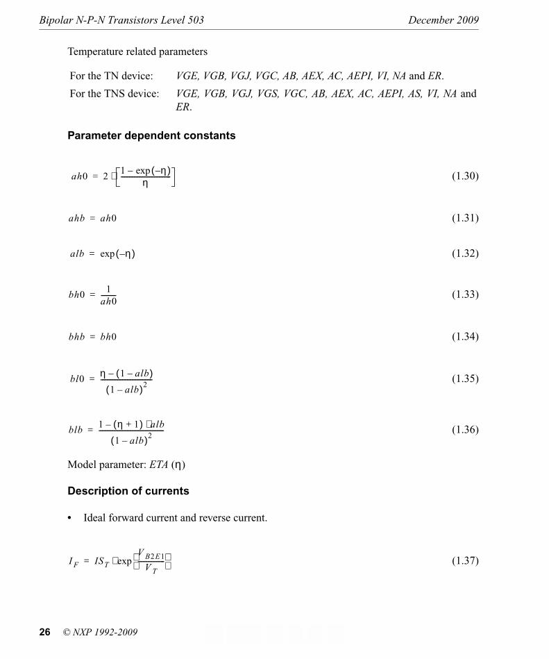
Temperature related parameters
Parameter dependent constants
(1.30)
(1.31)
(1.32)
(1.33)
(1.34)
(1.35)
(1.36)
Model parameter: ETA (η)
Description of currents
• Ideal forward current and reverse current.
(1.37)
For the TN device: VGE, VGB, VGJ, VGC, AB, AEX, AC, AEPI, VI, NA and ER.
For the TNS device: VGE, VGB, VGJ, VGS, VGC, AB, AEX, AC, AEPI, AS, VI, NA and ER.
ah0 21 η–( )exp–
η------------------------------⋅=
ahb ah0=
alb η–( )exp=
bh0 1ah0---------=
bhb bh0=
bl0 η 1 alb–( )–
1 alb–( )2-------------------------------=
blb 1 η 1+( ) alb⋅–
1 alb–( )2---------------------------------------=
I F IST
V B2E1
V T----------------
exp⋅=
26 © NXP 1992-2009 TOC Index Quitfile
ttt
t

December 2009 Bipolar N-P-N Transistors Level 503
(1.38)
Model parameter: IS
• The main current IN
The Moll-Ross formulation is used to take into account high injection in the base. To avoid dividing by zero the depletion charge term is modified.
(1.39)
(1.40)
(1.41)
Model parameter: QB0
Note3The depletion charges QTE , QTC , QBE and QBC are given by Eqs. 1.83, 1.87, 1.96 and 1.99respectively.
• Forward base currents. The total ideal base current is separated into a bulk and sidewall component. The bulk com-ponent depends on voltage VB2E1 and the sidewall component on voltage VB1E1. The separa-tion is given by parameter XIBI.
Bulk component:(1.42)
I R IST
V B2C2
V T----------------
exp⋅=
q0 1QTE QTC+
QB0T---------------------------+=
q1
q0 q02
K++
2--------------------------------=
q2
QBE QBC+
QB0T----------------------------=
I N
I F I R–
q1 q2+-----------------=
I B1 1 XIBI–( )IST
BFT-----------
V B2E1
V T----------------
exp 1–
⋅ ⋅=
© NXP 1992-2009 27TOC Index Quitfile
ttt
t

Bipolar N-P-N Transistors Level 503 December 2009
The non-ideal base current is given by:
(1.44)
Model parameters: IS, BF, XIBI, IBF and VLF
• Reverse base currents. In TN/TNS-level-503 the non-ideal reverse current is part of the basic Mextram model.
(1.45)
The extrinsic base current (electrons injected from collector to extrinsic base) is given by:
Sidewall component:(1.43)
For the TNS-device:
The substrate current (holes injected from base to substrate), including high injection is given by:
(1.46)
Note that the knee of the substrate current is projected on the emitter current, therefore in the square root: 4 ⋅ IST / IKST
(1.47)
I B1S
XIBIIST
BFT-----------
V B1E1
V T----------------
exp 1–
⋅ ⋅=
I B2 IBFT
V B2E1
V T----------------
exp 1–
V B2E1
2 V T⋅----------------
expVLFT
2 V T⋅---------------
exp+
--------------------------------------------------------------------
GMIN V B2E1⋅+⋅=
I B3 IBRT
V B1C1
V T----------------
exp 1–
V B1C1
2 V T⋅----------------
expVLRT
2 V T⋅---------------
exp+
--------------------------------------------------------------------
GMIN V B1C1⋅+⋅=
I SUB
2 ISST
V B1C1
V T----------------
exp 1–
⋅ ⋅
1 1 4IST
IKST-------------
V B1C1
V T----------------
exp
⋅ ⋅++
---------------------------------------------------------------------------------------=
I SF ISST
V SC1
V T-------------
exp 1–
⋅=
28 © NXP 1992-2009 TOC Index Quitfile
ttt
t

December 2009 Bipolar N-P-N Transistors Level 503
(1.48)
Model parameters: For the TN-device: IBR, VLR, BRI, IS, ETA, IK For the TNS-device: IBR, VLR, ISS IKS, BRI, IS, ETA, IK
• Weak avalanche current if IN ≤ 0 or ICAP ≤ 0 then IAVL = 0 The current ICAP is defined by Eqn. 1.85 or 1.86 respectively. At low current level the internal junction voltage is;
(1.49)
If Vj > - 0.9 ⋅ VDCT then
(1.50)
(1.51)
(1.52)
g1
4 IST aho( )2 V B1C1
V T----------------
exp⋅ ⋅ ⋅
IKT alb( )2⋅--------------------------------------------------------------------------=
nBEX albg1
2 1 1 g1++( )⋅-----------------------------------------⋅=
gEX1
BRI----------=
I EX gEX
alb nBEX+
ahb nBEX+-----------------------------
IKT
ahb---------- nBEX IST–⋅ ⋅
⋅=
V J V– B2C1 I CAP RCV T⋅–=
WDEPI
AVLT
Bn XPT⋅----------------------=
FC1–
1 XPT–( )1
I CAP
IHC------------–
MC
1V J
VDCT----------------+
PC-------------------------------------- XPT+⋅=
W D FC
AVLT
Bn--------------⋅=
© NXP 1992-2009 29TOC Index Quitfile
ttt
t

Bipolar N-P-N Transistors Level 503 December 2009
(1.53)
(1.54)
(1.55)
If EXAVL = 0 then EM = E0
The generation of avalanche current increases at high current levels. This is taken into account when flag EXAVL=1.
If EXAVL = 1 then
(1.56)
(1.57)
(1.58)
EC and IC1C2 are given by Eqn. 1.67, 1.80 or 1.81 respectively.
The intersection point XD and the avalanche current become:
dEWD FC VDCT
Bn
AVLT--------------⋅ ⋅=
E0
V J VDCT+
W D----------------------------- dEWD 1
I CAP
IHC------------–
I CAP RCV T⋅WDEPI
---------------------------------+⋅+=
E1
V J VDCT+
W D-----------------------------
I CAP RCV T⋅WDEPI
---------------------------------+=
X I
W EPI--------------
EC
I C1C2 RCV T⋅-----------------------------------=
SH W 1 2 SFH 1 2X I
W EPI--------------⋅+
⋅ ⋅+=
E2
V– B2C1 VDCT+
W D 1X I
2 W EPI⋅---------------------–
2⋅
----------------------------------------------------- dEWD 1X I
W EPI--------------–
EFII N
IHC SH W⋅----------------------------–
⋅ ⋅–=
EM E0
E2 E0 E2 E0–( )2CK I CAP I HC⁄ E1
2⋅ ⋅++–
2-----------------------------------------------------------------------------------------------------------------+=
30 © NXP 1992-2009 TOC Index Quitfile
ttt
t

December 2009 Bipolar N-P-N Transistors Level 503
(1.59)
(1.60)
(1.61)
(1.62)
If Vj ≤ - 0.9 ⋅ VDCT then IAVL=0
Model parameters: AVL , EFI, XP, MC, PC, VDC, RCV, IHC, SFH
Note3The variable intrinsic base resistance RB2 and the base charge terms q1 and q2 are given by Eqs. 1.63, 1.39 and 1.40 respectively.
• Series resistances:
• Variable base resistance The variable part of the base resistance is modulated by the base charges and takes into account the base current crowding:
(1.63)
(1.64)
emitter: RE = constant
collector: RCCT = constant
base: RBCT = constant
X D
EM W D⋅2 EM E1–( )⋅---------------------------------=
GEM
An
Bn------ EM X D
B– n
EM---------
expB– n
EM--------- 1
W D
X D---------+
⋅ exp–
⋅ ⋅ ⋅=
GMAX
V T
I N RBCT RB2+( )⋅-------------------------------------------------
q1 q2+
BFT----------------- RE
RBCT RB2+---------------------------------+ +=
I AVL I N
GEM GMAX⋅GEM 1 GMAX+( ) GMAX+⋅--------------------------------------------------------------------⋅=
RB23 RBV T⋅q1 q2+
-----------------------=
I B1B2
2 V T⋅RB2
---------------V B1B2
V T----------------
exp 1– V B1B2
RB2----------------+⋅=
© NXP 1992-2009 31TOC Index Quitfile
ttt
t

Bipolar N-P-N Transistors Level 503 December 2009
The base charge terms q1 and q2 are given by Eqs. 1.39 and 1.40 respectively.
Model parameter: RBV
• Variable collector resistance. This model of the epilayer resistance takes into account:
– The decrease in resistance due to carriers injected from the base if only the internal base-collector junction is forward biased (quasi-saturation) and if both the internal and exter-nal base-collector junction are forward biased (reverse mode of operation).
– Ohmic current flow at low current densities.– Space charge limited current flow at high current densities.– Current spreading in the epilayer.
The epilayer current is computed by solving a cubic equation.
(1.65)
(1.66)
(1.67)
If VB2C2 - VB2C1 > 0 (forward mode) then
(1.68)
(1.69)
(1.70)
(1.71)
K0 1 4 V B2C2 VDCT–( ) V T⁄[ ]exp⋅+=
KW 1 4 V B2C1 VDCT–( ) V T⁄[ ]exp⋅+=
EC V T K0 KW–K0 1+
KW 1+------------------
ln–⋅=
SF2 SFH⋅1 SFH+---------------------=
VV B2C2 V B2C1–
IHC RCV T⋅---------------------------------------=
EEC
IHC RCV T⋅--------------------------------=
RRCV T
SCRCV--------------------=
32 © NXP 1992-2009 TOC Index Quitfile
ttt
t

December 2009 Bipolar N-P-N Transistors Level 503
(1.72)
(1.73)
(1.74)
(1.75)
(1.76)
(1.77)
(1.78)
(1.79)
(1.80)
The argument of the square root of Eqn. 1.77 may become negative. Then s, s1 and s2 are complex. The magnitude of the imaginary part of s1 and s2 are equal and differ in sign.
If VB2C2 - VB2C1 ≤ 0 (reverse mode) then:
(1.81)
Model Parameters: IHC, RCV, SCRCV, SFH, VDC
A2 2– E V R V2
E+⋅+1 V+
------------------------------------–⋅=
A1
E2
3 V+( ) 2 E V SF E R V2⋅ ⋅ ⋅–⋅ ⋅+⋅
1 V+-------------------------------------------------------------------------------------------------=
A0E
2E V+( )⋅
1 V+------------------------------–=
q A1 3⁄ A22
9⁄–=
r A1 A2 3 A0⋅–⋅( ) 6 A23
27⁄–⁄=
s q3
r2
+=
s1 r s+( )1 3⁄=
s2 r s–( )1 3⁄=
I C1C2 IHC s1 s2 A2 3⁄–+( )⋅=
I C1C2
EC V B2C2 V B2C1–+
RCV T----------------------------------------------------=
© NXP 1992-2009 33TOC Index Quitfile
ttt
t

Bipolar N-P-N Transistors Level 503 December 2009
Description of charges
• Emitter depletion charge QTE
The total base-emitter depletion charge depends on VB2E1 :
(1.82)
The total base-emitter depletion capacitance is separated into a bulk and sidewall component. The bulk component is located between node E1 and node B2 and the sidewall component between nodes B1 and E1 (see Figure 1).
(1.83)
(1.84)
Model parameters : CJE , VDE , PE , XCJE
• Intrinsic collector depletion charge
If VB2C2 - VB2C1 > 0 then
(1.85)
If VB2C2 - VB2C1 ≤ 0 then:
(1.86)
QTEtot CJET VDET 1 K+( )⋅ ⋅
1 PE– K+--------------------------------------------------------- 1
1 K+( )
PE2
--------
1V B2E1
VDET----------------–
⋅
1V B2E1
VDET----------------–
2K+
PE2
--------
-----------------------------------------------------------------–⋅=
QTE 1 XCJE–( ) QTEtot⋅=
QTEs
XCJE QTEtot⋅=
QTC1
I CAP
IHC V B2C2 V B2C1–( )⋅V B2C2 V B2C1 IHC RCV T⋅+–-----------------------------------------------------------------------------=
CKI CKI CAP
IHC------------+=
I CAP
V B2C2 V B2C1–
RCV T---------------------------------------=
CKI CK=
34 © NXP 1992-2009 TOC Index Quitfile
ttt
t

December 2009 Bipolar N-P-N Transistors Level 503
The base-collector depletion charge is divided into a constant part (parameter XP) and a vari-able part. The constant part represents the finite thickness of the epilayer. The depletion charge is a function of the internal and external base-collector junction voltage.
(1.87)
Parameters: XCJC, CJC, VDC, PC, XP , MC , RCV, IHC
• Collector transit time in quasi-saturation ∆ QSAT
The current through the epilayer (Eqn. 1.80) without injection (EC=0) is:
To force the same current IC1C2 through the epilayer without injection, we need an epilayer voltage of V(EC=0):
The differential resistance R(EC=0) = ∂ V(EC=0) / ∂ IC1C2 is given by:
The collector transit time in quasi-saturation now becomes:
VC1
1 CK+( )
PC2
--------
1V B2C2
VDCT----------------–
⋅
1V B2C2
VDCT----------------–
2CKI+
PC2
--------
---------------------------------------------------------------------- 1I CAP
IHC------------–
MC
⋅=
VCV
VDCT 1 XPT–( ) 1 CK+( )⋅ ⋅1 PC CK+–
------------------------------------------------------------------------- 1 VC1–( )⋅=
QTC1XCJC CJCT VCV XPT I CAP RCV T V B2C2–⋅( )⋅– ⋅ ⋅=
V C1C2 V B2C2 V B2C1–=
I EC 0=( )IHC SCRCV V C1C2 V C1C2
2+⋅ ⋅
SCRCV IHC RCV T V C1C2+⋅( )⋅-------------------------------------------------------------------------------------=
B1 0.5 SCRCV I C1C2 IHC–( )⋅ ⋅=
B2 SCRCV IHC RCV T I C1C2⋅ ⋅ ⋅=
V EC 0=( ) B1 B1 B1 B2+⋅+=
R EC 0=( )SCRCV V EC 0=( ) IHC RCV T⋅+( )2⋅
V2
EC 0=( ) 2 V EC 0=( ) IHC RCV T SCRCV IHC2
RCV T⋅ ⋅+⋅ ⋅ ⋅+--------------------------------------------------------------------------------------------------------------------------------------------------------------------=
© NXP 1992-2009 35TOC Index Quitfile
ttt
t

Bipolar N-P-N Transistors Level 503 December 2009
(1.88)
The total collector depletion and transit time charge is:
if IC1C2 > 0 then
(1.89)
if then
(1.90)
• Extrinsic collector depletion charges QTEX and XQTEX. The extrinsic collector depletion charge is partitioned between nodes B1 and C1 and nodes B and C1 respectively independent of flag EXMOD.
(1.91)
To the external base node is connected:
QSAT∆ R EC 0=( )
∂QT C1
∂V B2C2------------------- I C1C2 I EC 0=( )–( )⋅ ⋅=
QTC QTC1QSAT∆+=
I C1C2 0≤
QTC QTC1=
VTEX 1
1 CK+( )
PC2
--------
1V B1C1
VDCT----------------–
⋅
1V B1C1
VDCT----------------–
2CK+
PC2
--------
----------------------------------------------------------------------=
VTEX V
VDCT 1 XPT–( ) 1 CK+( )⋅ ⋅1 PC CK+–
------------------------------------------------------------------------- 1 VTEX 1–( )⋅=
QTEX 1 XEXT–( ) 1 XCJC–( ) CJCT VTEX V XPT V B1C1⋅+( )⋅ ⋅ ⋅=
36 © NXP 1992-2009 TOC Index Quitfile
ttt
t

December 2009 Bipolar N-P-N Transistors Level 503
(1.92)
Model parameters: XCJC, CJC, VDC, PC, XP , XEXT
• Stored base charges QBE and QBC
(1.94)
(1.95)
(1.96)
For the TNS-device:
• Depletion charge QTS.
(1.93)
Model parameters: CJS, VDS and PS
XVTEX 1
1 CK+( )
PC2
--------
1V BC1
VDCT----------------–
⋅
1V BC1
VDCT----------------–
2CK+
PC2
--------
---------------------------------------------------------------------=
XVTEX V
VDCT 1 XPT–( ) 1 CK+( )⋅ ⋅1 PC CK+–
------------------------------------------------------------------------- 1 XVTEX 1–( )⋅=
XQTEX XEXT 1 XCJC–( ) CJCT XVTEX V XPT V BC1⋅+( )⋅ ⋅ ⋅=
QTS
CJST VDST 1 K+( )⋅ ⋅1 PS– K+
-------------------------------------------------------- 1
1 K+( )
PS2
-------
1V SC1
VDST---------------–
⋅
1V SC1
VDST---------------–
2K+
PS2
-------
---------------------------------------------------------------–⋅=
QB q1 QB0T⋅=
f 1
4 IST aho( )2⋅ ⋅IKT
--------------------------------------V B2E1
V T----------------
exp⋅=
n0
f 1
2 1 1 f 1++( )⋅-----------------------------------------=
QBE QB n0
12---
aho4
--------- n0+ +
12--- aho
4---------+
bhoblo---------
n0+⋅-------------------------------------------------------------- bho⋅ ⋅ ⋅=
© NXP 1992-2009 37TOC Index Quitfile
ttt
t

Bipolar N-P-N Transistors Level 503 December 2009
(1.97)
(1.98)
(1.99)
Model parameters: QB0, IK, ETA, IS
• Neutral and emitter charge
(1.100)
(1.101)
Model parameters: TAUNE, MTAU, IS
• Stored epilayer charge
if then
(1.102)
The current IC1C2 is given by Eqn. 1.80 or 1.81 respectively.
if
f 2 4 IST aho( )2 V B2C2
V T----------------
exp IKT alb( )2⋅ ⁄⋅ ⋅ ⋅=
nB albf 2
2 1 1 f 2++( )⋅-----------------------------------------⋅=
QBC QB nB
alb blb nB+⋅alb bhb nB+⋅-----------------------------------
bhb⋅ ⋅ ⋅=
QN 0 TAUNET IKT
IST
IKT----------
1MTAU T---------------------
MTAU T 2 MTAU T–( )⋅⋅ ⋅ ⋅=
⋅MTAU T 1–
2 2 MTAU T–( )⋅------------------------------------------
1 1MTAU T---------------------–
QN QN 0
V B2E1
V T MTAU T⋅---------------------------------
exp 1–
⋅=
V B2C1 V B2C2– 1 108–⋅>
QEPI IST QB0T
V B2C2
V T----------------
expV B2C1
V T----------------
exp–
I C1C2---------------------------------------------------------------------⋅ ⋅=
V B2C1 V B2C2– 1 108–⋅>
38 © NXP 1992-2009 TOC Index Quitfile
ttt
t

December 2009 Bipolar N-P-N Transistors Level 503
(1.103)
(1.104)
(1.105)
Model parameters: QB0, RCV, VDC, IS
• Extrinsic charges
(1.106)
(1.107)
(1.108)
(1.109)
(1.110)
Model parameters: QB0, RCV, VDC, IS, XCJC
p0
2 V B2C2 VDCT–( ) V T⁄exp ⋅1 K0+( )
------------------------------------------------------------------------------=
pw
2 V B2C1 VDCT–( ) V T⁄exp ⋅1 KW+( )
------------------------------------------------------------------------------=
QEPI RCV T IST QB0T
VDCT
V T----------------
expp0 pw+
2 V T⋅-------------------⋅ ⋅ ⋅ ⋅=
g2 4V B1C1 VDCT–
V T--------------------------------------
exp⋅=
pWEX
g2
2 1 1 g2++[ ]⋅-----------------------------------------=
g3
RCV T IST
VDCT
V T----------------
exp⋅ ⋅
V T-----------------------------------------------------------------=
g4
alb blb nBEX+⋅alb bhb nBEX+⋅------------------------------------------ bhb⋅=
QEX QB0T1 XCJC–
XCJC-------------------------
g3 pWEX g4 nBEX⋅+⋅( )⋅ ⋅=
© NXP 1992-2009 39TOC Index Quitfile
ttt
t

Bipolar N-P-N Transistors Level 503 December 2009
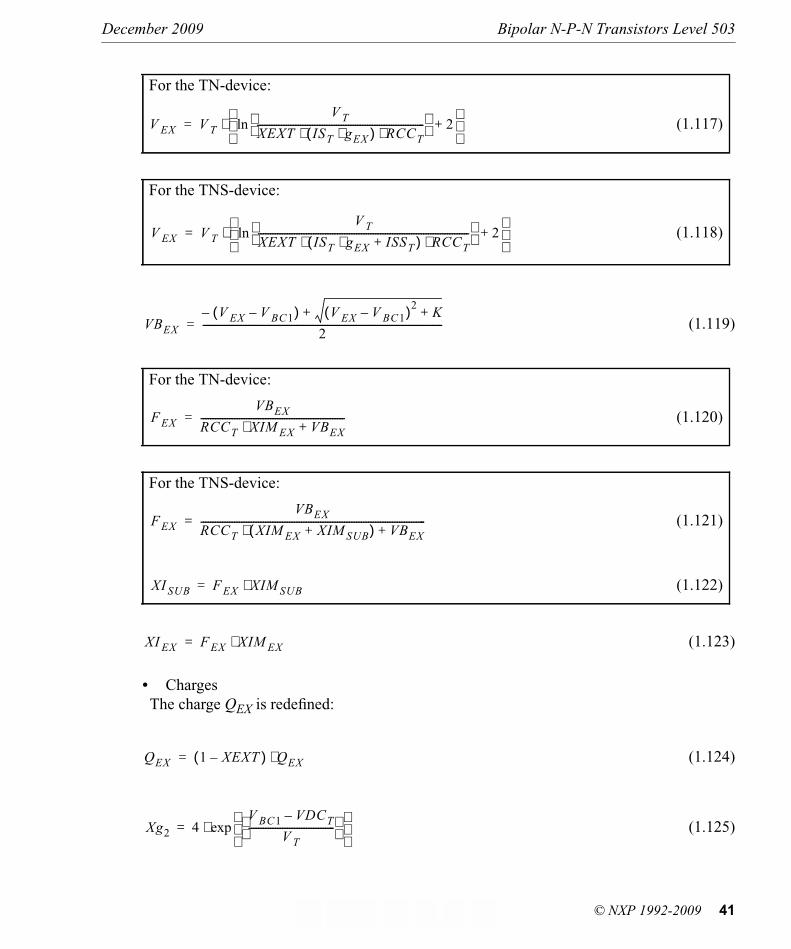
Extended modeling of the reverse current gain EXMOD=1
• Currents The base current IEX is redefined
(1.111)
A part XEXT of the base current of the extrinsic transistor is connected to the base terminal:
(1.114)
(1.115)
(1.116)
To improve convergency behaviour the conductivity of branch b-c1 is limited to 1 / RCCT.
For the TNS-device:
The base current ISUB is redefined:
(1.112)
For the TNS-device:
(1.113)
I EX 1 XEXT–( ) I EX⋅=
I SUB 1 XEXT–( ) I SUB⋅=
XIM SUB XEXT
2 ISST
V BC1
V T-------------
exp 1–
⋅ ⋅
1 1 4IST
IKST-------------
V BC1
V T-------------
exp
⋅++
--------------------------------------------------------------------------------⋅=
Xg1
4 IST aho( )2 V BC1
V T-------------
exp⋅ ⋅ ⋅
IKT alb( )2⋅-----------------------------------------------------------------------=
X nBEX albXg1
2 1 1 Xg1++[ ]⋅---------------------------------------------⋅=
XIM EX XEXT gEX
alb X nBEX+
ahb X nBEX+----------------------------------
IKT
ahb---------- XnBEX IST–⋅ ⋅
⋅ ⋅=
40 © NXP 1992-2009 TOC Index Quitfile
ttt
t
December 2009 Bipolar N-P-N Transistors Level 503
(1.119)
(1.123)
• Charges The charge QEX is redefined:
(1.124)
(1.125)
For the TN-device:
(1.117)
For the TNS-device:
(1.118)
For the TN-device:
(1.120)
For the TNS-device:
(1.121)
(1.122)
V EX V T
V T
XEXT IST gEX⋅( ) RCCT⋅ ⋅----------------------------------------------------------------------
ln 2+
⋅=
V EX V T
V T
XEXT IST gEX ISST+⋅( ) RCCT⋅ ⋅----------------------------------------------------------------------------------------
ln 2+
⋅=
VBEX
V EX V BC1–( )– V EX V BC1–( )2K++
2----------------------------------------------------------------------------------------------------=
F EX
VBEX
RCCT XIM EX VBEX+⋅------------------------------------------------------------=
F EX
VBEX
RCCT XIM EX XIM SUB+( ) VBEX+⋅----------------------------------------------------------------------------------------------=
XI SUB F EX XIM SUB⋅=
XI EX F EX XIM EX⋅=
QEX 1 XEXT–( ) QEX⋅=
Xg2 4V BC1 VDCT–
V T------------------------------------
exp⋅=
© NXP 1992-2009 41TOC Index Quitfile
ttt
t

Bipolar N-P-N Transistors Level 503 December 2009
(1.126)
(1.127)
(1.128)
Model parameter: XEXT
Note3The depletion charges QTEX and XQTEX are distributed always over the internal and exter-nal base node independent of EXMOD.
Distributed high frequency effects in the intrinsic base
Distributed high frequency effects are modeled, in first order approximation, both in lateral direction (current crowding) and in vertical direction (excess phase shift). The distributed effects are part of the Mextram model and can be switched on/off with the flag EXPHI. The high frequency current crowding is modeled by;
(1.129)
(1.130)
For simplicity reasons only the forward depletion and diffusion charges are taken into account. The partial derivative of QB1B2 with respect to VB2E1 has to be neglected in AC anal-ysis. In transient analysis (if EXPHI=1) the convergency behaviour may be improved by approximating this derivative with
(1.131)
XpWEX
Xg2
2 1 1 Xg2++[ ]⋅---------------------------------------------=
Xg4
alb blb XnBEX+⋅alb bhb XnBEX+⋅---------------------------------------------- bhb⋅=
XQEX F EX XEXT QB0T1 XCJC–
XCJC------------------------- g3 XpWEX⋅( ) Xg4 XnBEX⋅( )+ ⋅ ⋅ ⋅ ⋅=
CB15---
∂QTE
∂V B2E1-------------------
∂QBE
∂V B2E1-------------------
∂QN
∂V B2E1-------------------+ +
⋅=
QB1B2 CB V B1B2⋅=
∂QB1B2
∂V B2E1-------------------
∂QBE
∂V B2E1-------------------
∂QN
∂V B2E1-------------------+
V B1B2
5 V T⋅----------------
⋅=
42 © NXP 1992-2009 TOC Index Quitfile
ttt
t

December 2009 Bipolar N-P-N Transistors Level 503
In vertical direction (excess phase shift) base-charge-partitioning is used. For simplicity rea-sons it is only implemented for the forward base charge (QBE) and for low level injection. Now QBE (Eqn. 1.96) and QBC (Eqn. 1.99) are redefined according to;
(1.132)
(1.133)
(1.134)
For the partitioning factor qC is 1/3.
Noise model
For noise analysis noise current sources are added to the small signal equivalent circuit. In these equations f represents the operation frequency of the transistor and ∆ f is the bandwidth. When ∆ f is taken as 1 Hz, a noise density is obtained.
Thermal noise:
• Emitter Resistor
Emitter Resistor Noise
(1.135)
• Base Resistor
(1.136)
For the variable part of the base resistance a different formula is used, taking into account the effect of current crowding on noise behaviour:
QBE' 1 qC–( ) QBE⋅=
QBC' qC QBE QBC+⋅=
qC2 η 2 η–( ) η( )exp⋅–+
2 η 1 η–( ) η( )exp⋅ η–( )exp–––--------------------------------------------------------------------------------------=
η 0=
iN RE2 4 k T K⋅ ⋅
RE---------------------- f∆⋅=
iN RBC2 4 k T K⋅ ⋅
RBCT---------------------- f∆⋅=
© NXP 1992-2009 43TOC Index Quitfile
ttt
t

Bipolar N-P-N Transistors Level 503 December 2009
(1.137)
Base Resistor Noise
(1.138)
• Collector Resistor
Collector Resistor Noise
(1.139)
For the variable part of the base resistance a different formula is used, taking into account the effect of current crowding on noise behaviour:
• Collector Current
Collector current shot noise:
(1.140)
• Base Current
Forward base current shot noise and 1/f noise:
(1.141)
Emitter-base sidewall current shot noise and 1/f noise:
(1.142)
iN RBV2 5.26 k T K⋅ ⋅
RB2------------------------------ 1 2
V B1B2
V T----------------
exp⋅+
34---
f∆⋅ ⋅=
iN RB2
iN RBV2
iN RBC2
+=
iN RCC2 4 k T K⋅ ⋅
RCCT---------------------- f∆⋅=
iN C2
2 q I N f∆⋅ ⋅ ⋅=
iN B2
2q I B1 I B2+[ ] MULTf
----------------- KFNI B2
MULT-----------------
2
KFI B1
MULT-----------------
AF
++
f∆⋅=
iN BS2
2 q I B1S MULT
f----------------- KF
I B1S
MULT-----------------
AF
⋅ ⋅+⋅ ⋅
f∆⋅=
44 © NXP 1992-2009 TOC Index Quitfile
ttt
t

December 2009 Bipolar N-P-N Transistors Level 503
Reverse base current shot noise and 1/f noise:
(1.143)
Base Current Shot Noise
(1.144)
• Extrinsic Current
Extrinsic current shot noise and 1/f noise:
(1.145)
If EXMOD = TRUE we also have:
(1.146)
Extrinsic Current Shot Noise
(1.147)
iN B32
2 q I B3MULT
f----------------- KF
I B3
MULT-----------------
AF
⋅ ⋅+⋅ ⋅
f∆⋅=
iN RB2
iN B2
iN BS2
+ iN B32
+=
iN IEX2
2 q I EXKF
f--------
I EX
MULT-----------------
AF
MULT⋅ ⋅+⋅ ⋅
f∆⋅=
iN XIEX2
2 q XI EXKF
f--------
XI EX
MULT-----------------
AF
MULT⋅ ⋅+⋅ ⋅
f∆⋅=
iN EX2
iN IEX2
iN XIEX2
+=
© NXP 1992-2009 45TOC Index Quitfile
ttt
t

Bipolar N-P-N Transistors Level 503 December 2009
46 © NXP 1992-2009 TOC Index Quitfile
ttt
t

December 2009 Hyp functions
A Hyp functions
1151TOC Index Quitfile
ttt
t

Hyp functions December 2009
Figure 86:
Figure 87:
0 X
ε
hyp1
hyp1 x ε;( ) 12--- x x
2 4 ε2⋅++( )⋅=
0
ε
hyp2
x0
x0 x
hyp2 x x0; ε;( ) x hyp1 x x0– ε;( )–=
1152 TOC Index Quitfile
ttt
t

December 2009 Hyp functions
Figure 88:
Figure 89:
0 x0 x
hyp3
εxo+hyp1(-xo;ε)
hyp3 x x0; ε;( ) hyp2 x x0; ε;( ) hyp2 0 x0; ε;( )–= for ε ε x0( )=
0
x
hyp4
ε
-hyp1(-xo;ε) xo
hyp4 x x0; ε;( ) hyp1 x x0– ε;( ) hyp1 x0– ε;( )–=
1153TOC Index Quitfile
ttt
t

Hyp functions December 2009
Figure 90:
The hypm-function:
(18.133)
setlengthunitlength0.40900pt beginpicture(1500,900)(0,0) enrm hinlines drawline[-50](264,158)(1436,158) hinlines drawline[-50](264,158)(264,787) hicklines path(264,158)(264,178)hicklines path(264,787)(264,767) put(264,113)makebox(0,0)0 hicklines path(264,158)(1436,158)(1436,787)(264,787)(264,158) put(45,472)makebox(0,0)[l]shortstackhyp
0
x0ε
xo
hyp5
x
hyp5 x x0; ε;( ) x0 hyp1 x0 x ε2
x0-----–– ε,
–= for ε ε x0( )=
hypm x, y;m[ ] x y⋅
x2 m⋅
y2 m⋅
+( )1 2 m⋅( )⁄-----------------------------------------------------=
1154 TOC Index Quitfile
ttt
t

December 2009 Spectre Specific Information
B Spectre Specific Information
1155TOC Index Quitfile
ttt
t

Spectre Specific Information December 2009
Imax, Imelt, Jmelt parameters
IntroductionImax, Imelt and Jmelt are Spectre-specific parameters used to help convergence and to pre-vent numerical problems. We refer in this text only to the use of Imax model parameter inSpectre with SiMKit devices since the other two parameters, Imelt and Jmelt, are not part ofthe SiMKit code. For information on Imelt and Jmelt refer to Cadence documentation.
Imax model parameterImax is a model parameter present in the following SiMKit models:– juncap and juncap2– psp and pspnqs (since they contain juncap models)
In Mextram 504 (bjt504) and Modella (bjt500) SiMKit models, Imax is an internal parameterand its value is set through the adapter via the Spectre-specific parameter Imax.
In models that contain junctions, the junction current can be expressed as:
(18.134)
The exponential formula is used until the junction current reaches a maximum (explosion)current Imax.
(18.135)
The corresponding voltage for which this happens is called Vexpl (explosion voltage). Thevoltage explosion expression can be derived from (1):
(18.136)
For the following linear expression is used for the junction current:
I I sV
N φTD⋅------------------ 1–
exp=
I max I s
V lexp
N φTD⋅------------------ 1–
exp=
V lexp N φTD
I max
I s----------
1+log⋅=
V V lexp>
1156 TOC Index Quitfile
ttt
t

December 2009 Spectre Specific Information
(18.137)
The default value of the Imax model parameter for SiMKit is 1000A. The default value ofImax for Mextram 504 and Modella is 1A. Imax should be set to a value which is largeenough so it does not affect the extraction procedure.
Region parameter
Region is an Spectre-specific model parameter used as a convergence aid and gives an esti-mated DC operating region. The possible values of region depend on the model:
– For Bipolar models:– subth: Cut-off or sub-threshold mode– fwd: Forward– rev: Reverse– sat: Saturation.– off1
–– For MOS models:
– subth: Cut-off or sub-threshold mode;– triode: Triode or linear region;– sat: Saturation– off1
For PSP and PSPNQS all regions are allowed, as the PSP(NQS) models both have a MOSpart and a juncap (diode). Not all regions are valid for each part, but when e.g. region=for-ward is set, the initial guesses for the MOS will be set to zero. The same holds for setting aregion that is not valid for the JUNCAP.
– For diode models:– fwd: Forward– rev: Reverse– brk: Breakdown– off1
1.Off is not an electrical region, it just states that the user does not know in what state thedevice is operating
I I max V V lexp–( )+I s
N φTD⋅------------------
V lexp
N φTD⋅------------------
exp=
1157TOC Index Quitfile
ttt
t

Spectre Specific Information December 2009
Model parameters for device reference temperature in Spectre
This text describes the use of the tnom, tref and tr model parameters in Spectre with SiMKitdevices to set the device reference temperature.
A Simkit device in Spectre has three model parameter aliases for the model reference temper-ature, tnom, tref and tr. These three parameters can only be used in a model definition, not asinstance parameters.
There is no difference in setting tnom, tref or tr. All three parameters have exactly the sameeffect. The following three lines are therefore completely equivalent:
model nmos11020 mos11020 type=n tnom=30 model nmos11020 mos11020 type=n tref=30 model nmos11020 mos11020 type=n tr=30
All three lines set the reference temperature for the mos11020 device to 30 C.
Specifying combinations of tnom, tref and tr in the model definition has no use, only thevalue of the last parameter in the model definition will be used. E.g.:
model nmos11020 mos11020 type=n tnom=30 tref=34
will result in the reference temperature for the mos11020 device being set to 34 C, tnom=30will be overridden by tref=34 which comes after it.
When there is no reference temperature set in the model definition (so no tnom, tref or tr isset), the reference temperature of the model will be set to the value of tnom in the optionsstatement in the Spectre input file. So setting:
options1 options tnom=23 gmin=1e-15 reltol=1e-12 \ vabstol=1e-12 iabstol=1e-16 model nmos11020 mos11020 type=n
will set the reference temperature of the mos11020 device to 23 C.
When no tnom is specified in the options statement and no reference temperature is set in themodel definition, the default reference temperature is set to 27 C.So the lines:
options1 options gmin=1e-15 reltol=1e-12 vabstol=1e-12 \ iabstol=1e-16 model nmos11020 mos11020 type=n
1158 TOC Index Quitfile
ttt
t

December 2009 Spectre Specific Information
will set the reference temperature of the mos11020 device to 27 C.
The default reference temperature set in the SiMKit device itself is in the Spectre simulatornever used. It will always be overwritten by either the default "options tnom", an explicitlyset option tnom or by a tnom, tref or tr parameter in the model definition.
1159TOC Index Quitfile
ttt
t

Spectre Specific Information December 2009
1160 TOC Index Quitfile
ttt
t