bipolar transistor biasing circuits - ibiblio - the public's
TRANSCRIPT

Bipolar transistor biasing circuits
This worksheet and all related files are licensed under the Creative Commons Attribution License,version 1.0. To view a copy of this license, visit http://creativecommons.org/licenses/by/1.0/, or send aletter to Creative Commons, 559 Nathan Abbott Way, Stanford, California 94305, USA. The terms andconditions of this license allow for free copying, distribution, and/or modification of all licensed works bythe general public.
Resources and methods for learning about these subjects (list a few here, in preparation for yourresearch):
1
Questions
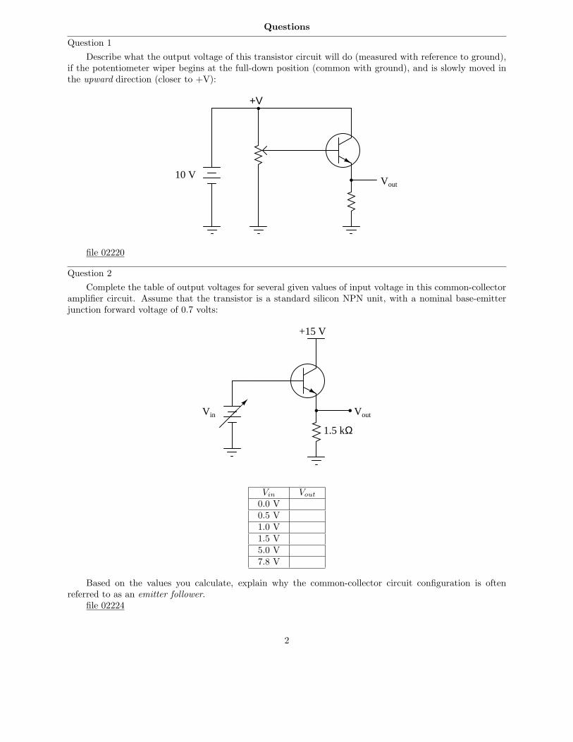
Question 1
Describe what the output voltage of this transistor circuit will do (measured with reference to ground),if the potentiometer wiper begins at the full-down position (common with ground), and is slowly moved inthe upward direction (closer to +V):
+V
Vout10 V
file 02220
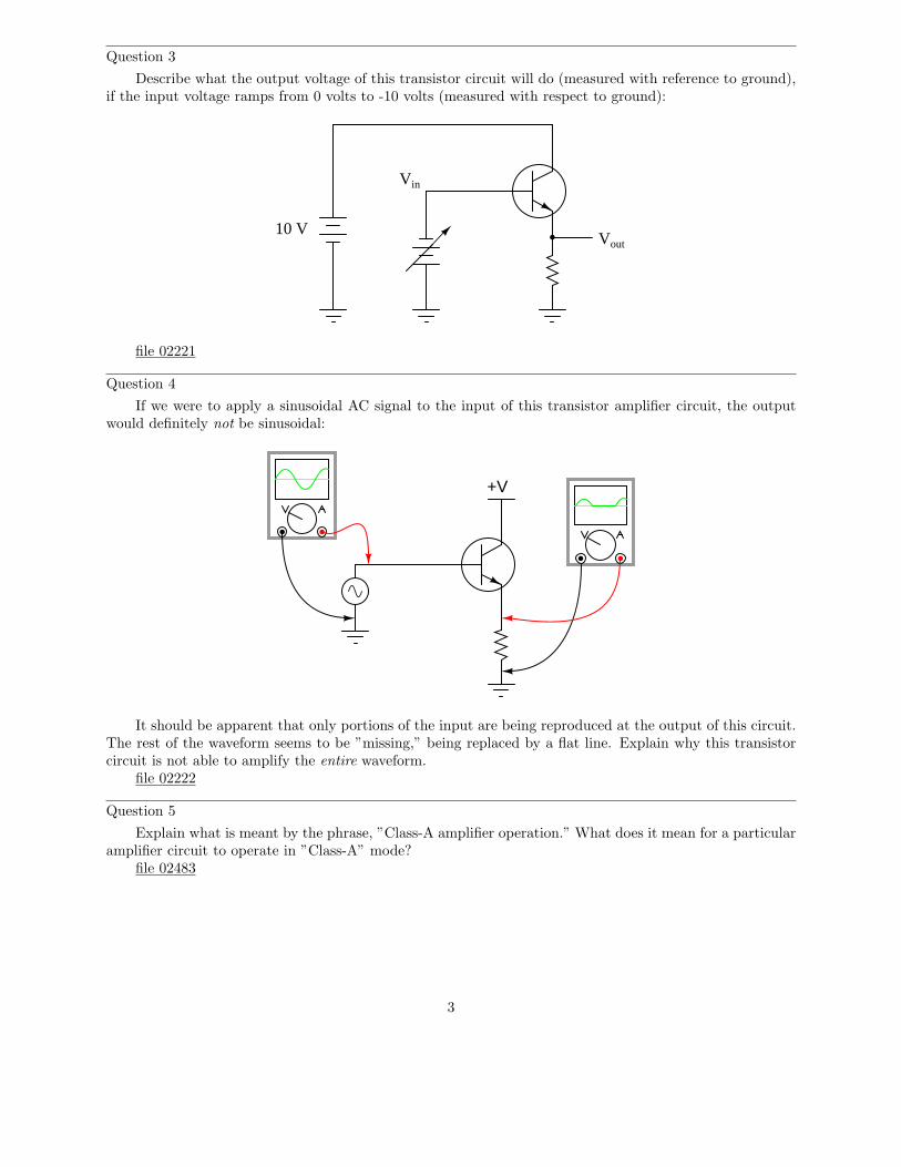
Question 2
Complete the table of output voltages for several given values of input voltage in this common-collectoramplifier circuit. Assume that the transistor is a standard silicon NPN unit, with a nominal base-emitterjunction forward voltage of 0.7 volts:
Vin Vout
+15 V
1.5 kΩ
Vin Vout
0.0 V0.5 V1.0 V1.5 V5.0 V7.8 V
Based on the values you calculate, explain why the common-collector circuit configuration is oftenreferred to as an emitter follower.
file 02224
2
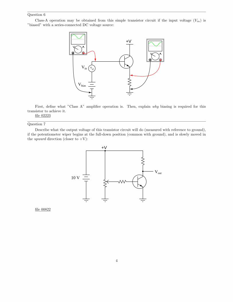
Question 3
Describe what the output voltage of this transistor circuit will do (measured with reference to ground),if the input voltage ramps from 0 volts to -10 volts (measured with respect to ground):
Vout10 V
Vin
file 02221
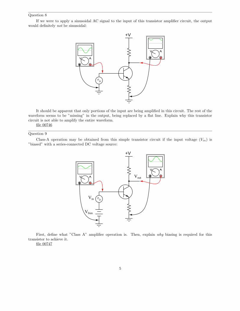
Question 4
If we were to apply a sinusoidal AC signal to the input of this transistor amplifier circuit, the outputwould definitely not be sinusoidal:
+V
It should be apparent that only portions of the input are being reproduced at the output of this circuit.The rest of the waveform seems to be ”missing,” being replaced by a flat line. Explain why this transistorcircuit is not able to amplify the entire waveform.
file 02222
Question 5
Explain what is meant by the phrase, ”Class-A amplifier operation.” What does it mean for a particularamplifier circuit to operate in ”Class-A” mode?
file 02483
3
Question 6
Class-A operation may be obtained from this simple transistor circuit if the input voltage (Vin) is”biased” with a series-connected DC voltage source:
+V
Vin
Vbias
First, define what ”Class A” amplifier operation is. Then, explain why biasing is required for thistransistor to achieve it.
file 02223
Question 7
Describe what the output voltage of this transistor circuit will do (measured with reference to ground),if the potentiometer wiper begins at the full-down position (common with ground), and is slowly moved inthe upward direction (closer to +V):
+V
Vout
10 V
file 00822
4
Question 8
If we were to apply a sinusoidal AC signal to the input of this transistor amplifier circuit, the outputwould definitely not be sinusoidal:
+V
It should be apparent that only portions of the input are being amplified in this circuit. The rest of thewaveform seems to be ”missing” in the output, being replaced by a flat line. Explain why this transistorcircuit is not able to amplify the entire waveform.
file 00746
Question 9
Class-A operation may be obtained from this simple transistor circuit if the input voltage (Vin) is”biased” with a series-connected DC voltage source:
+V
Vin
Vbias
Vout
First, define what ”Class A” amplifier operation is. Then, explain why biasing is required for thistransistor to achieve it.
file 00747
5
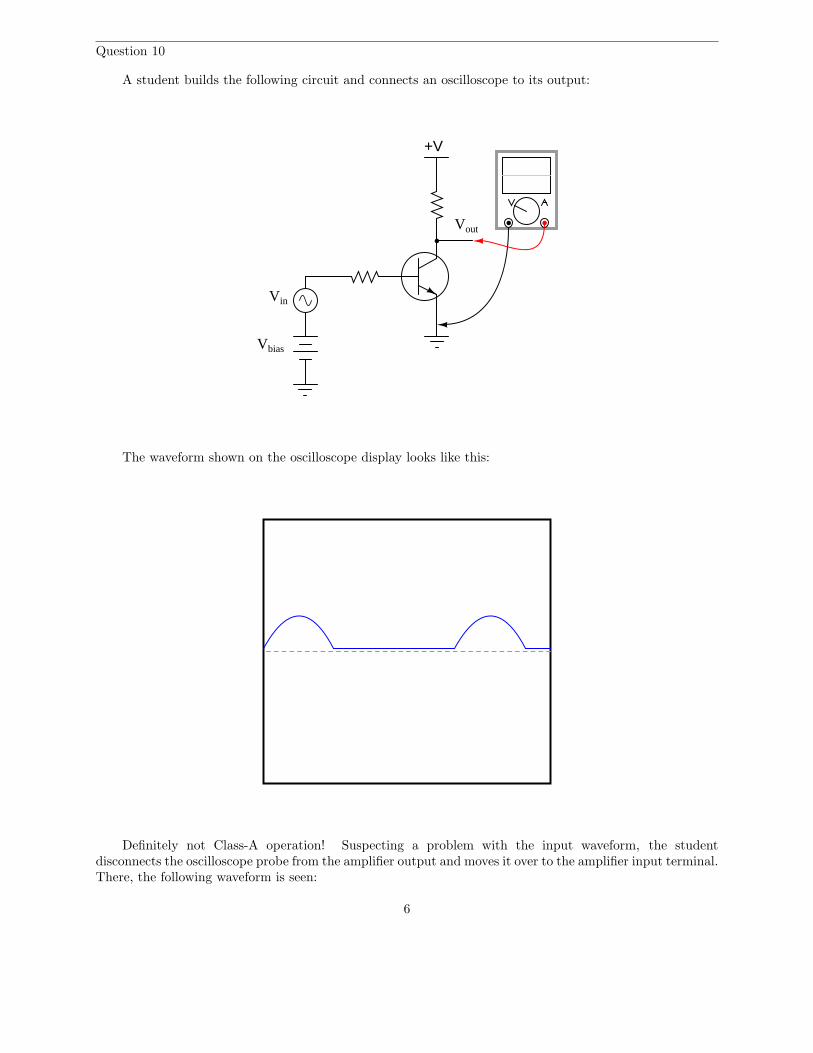
Question 10
A student builds the following circuit and connects an oscilloscope to its output:
+V
Vin
Vbias
Vout
The waveform shown on the oscilloscope display looks like this:
Definitely not Class-A operation! Suspecting a problem with the input waveform, the studentdisconnects the oscilloscope probe from the amplifier output and moves it over to the amplifier input terminal.There, the following waveform is seen:
6
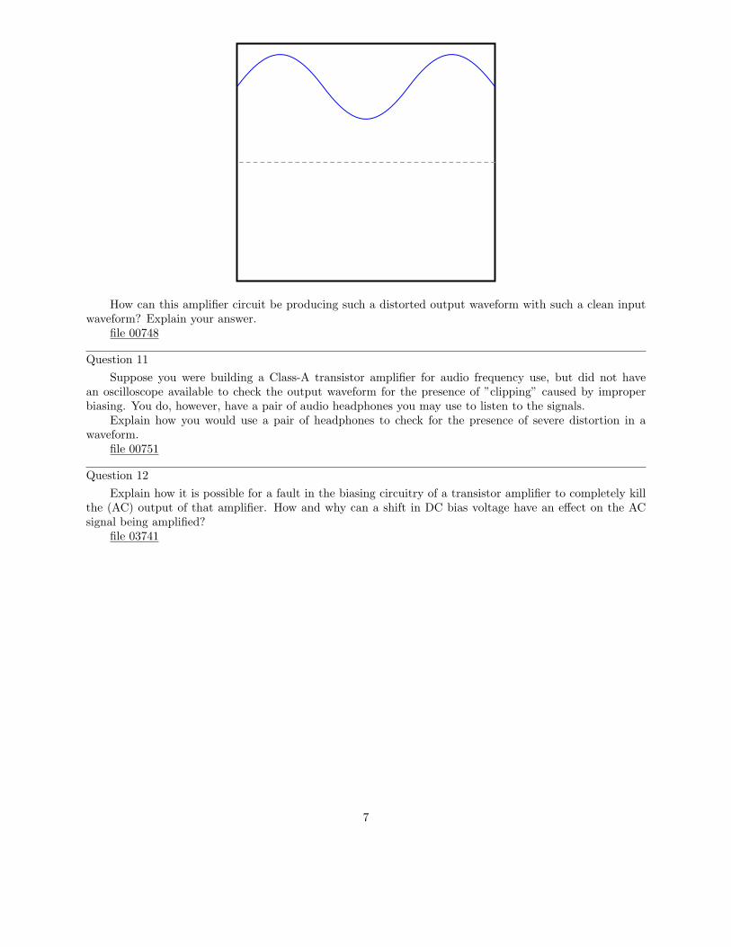
How can this amplifier circuit be producing such a distorted output waveform with such a clean inputwaveform? Explain your answer.
file 00748
Question 11
Suppose you were building a Class-A transistor amplifier for audio frequency use, but did not havean oscilloscope available to check the output waveform for the presence of ”clipping” caused by improperbiasing. You do, however, have a pair of audio headphones you may use to listen to the signals.
Explain how you would use a pair of headphones to check for the presence of severe distortion in awaveform.
file 00751
Question 12
Explain how it is possible for a fault in the biasing circuitry of a transistor amplifier to completely killthe (AC) output of that amplifier. How and why can a shift in DC bias voltage have an effect on the ACsignal being amplified?
file 03741
7
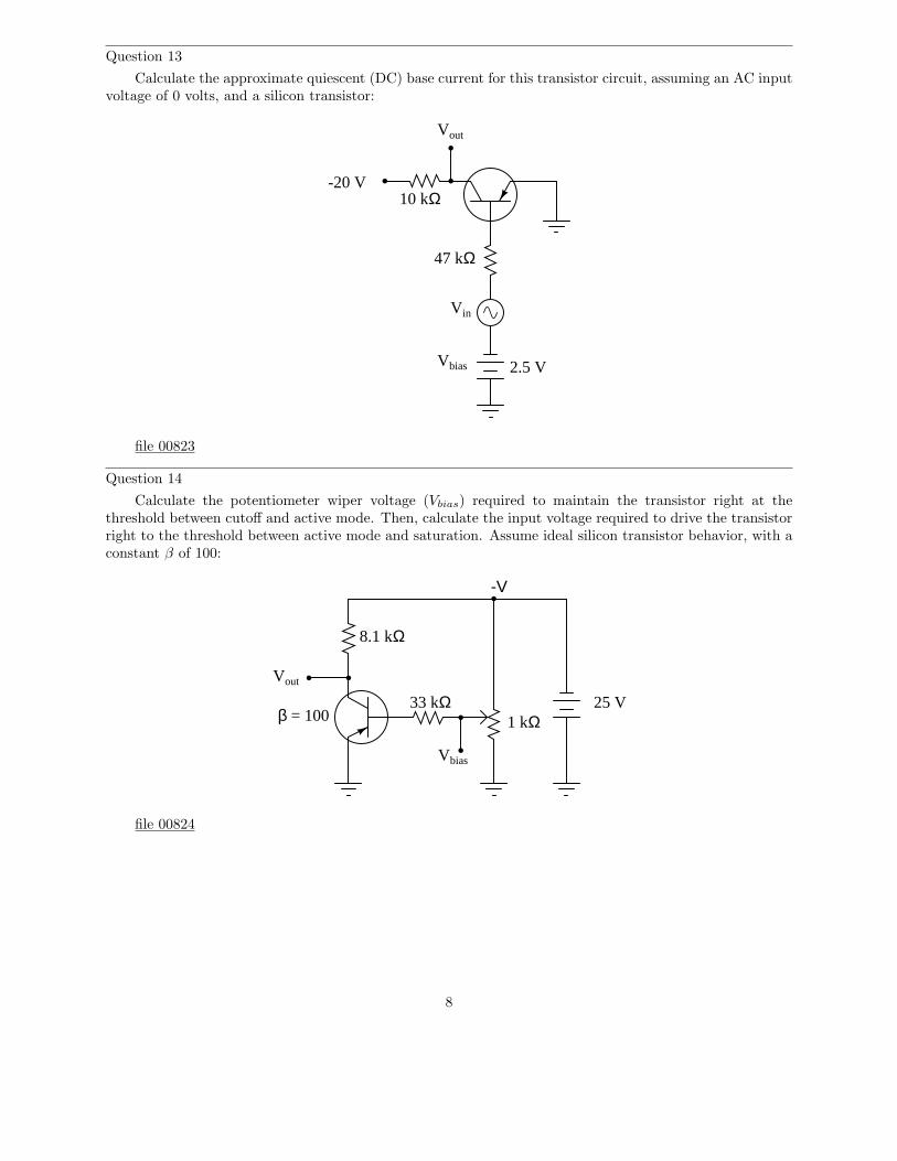
Question 13
Calculate the approximate quiescent (DC) base current for this transistor circuit, assuming an AC inputvoltage of 0 volts, and a silicon transistor:
Vin
Vbias
Vout
47 kΩ
-20 V
2.5 V
10 kΩ
file 00823
Question 14
Calculate the potentiometer wiper voltage (Vbias) required to maintain the transistor right at thethreshold between cutoff and active mode. Then, calculate the input voltage required to drive the transistorright to the threshold between active mode and saturation. Assume ideal silicon transistor behavior, with aconstant β of 100:
Vout
25 V
-V
1 kΩ
Vbias
33 kΩ
8.1 kΩ
β = 100
file 00824
8
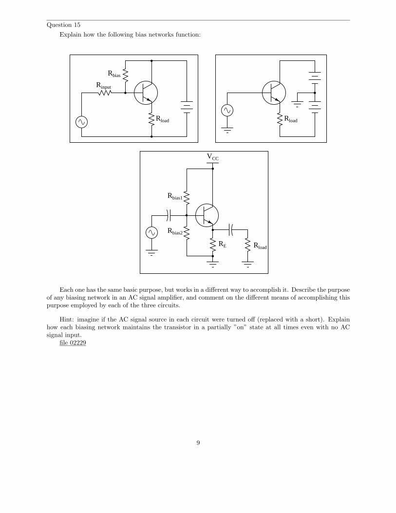
Question 15
Explain how the following bias networks function:
Rbias
Rinput
Rload
Rload
Rbias1
Rbias2
Rload
RE
VCC
Each one has the same basic purpose, but works in a different way to accomplish it. Describe the purposeof any biasing network in an AC signal amplifier, and comment on the different means of accomplishing thispurpose employed by each of the three circuits.
Hint: imagine if the AC signal source in each circuit were turned off (replaced with a short). Explainhow each biasing network maintains the transistor in a partially ”on” state at all times even with no ACsignal input.
file 02229
9
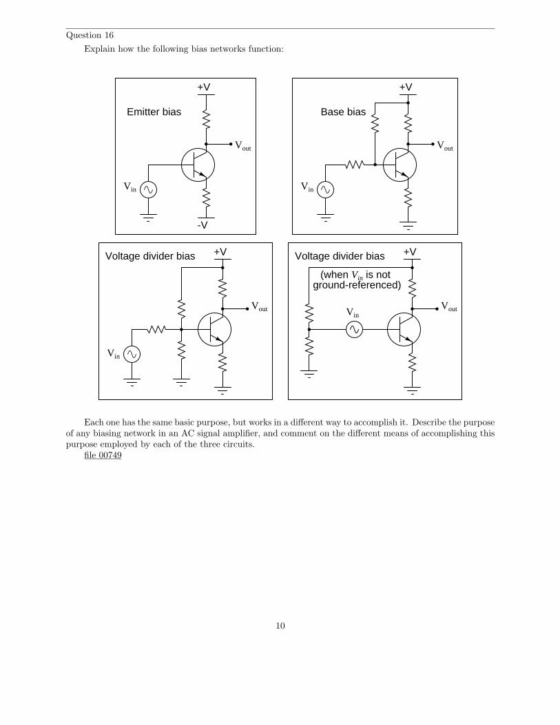
Question 16
Explain how the following bias networks function:
+V
Vin
Vout
-V
Emitter bias
+V
Vin
Vout
Base bias
+VVoltage divider bias +V
VinVout
Voltage divider bias
(when Vin is notground-referenced)
Vin
Vout
Each one has the same basic purpose, but works in a different way to accomplish it. Describe the purposeof any biasing network in an AC signal amplifier, and comment on the different means of accomplishing thispurpose employed by each of the three circuits.
file 00749
10
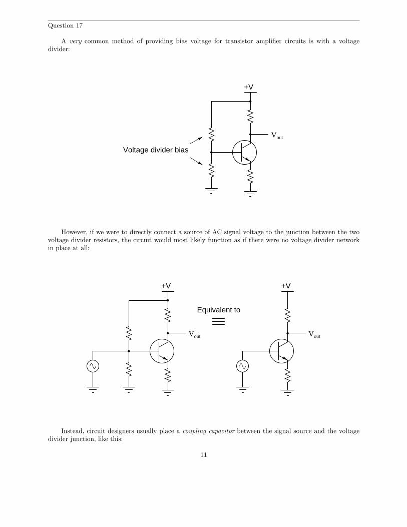
Question 17
A very common method of providing bias voltage for transistor amplifier circuits is with a voltagedivider:
+V
Vout
Voltage divider bias
However, if we were to directly connect a source of AC signal voltage to the junction between the twovoltage divider resistors, the circuit would most likely function as if there were no voltage divider networkin place at all:
+V
Vout
+V
Vout
Equivalent to
Instead, circuit designers usually place a coupling capacitor between the signal source and the voltagedivider junction, like this:
11
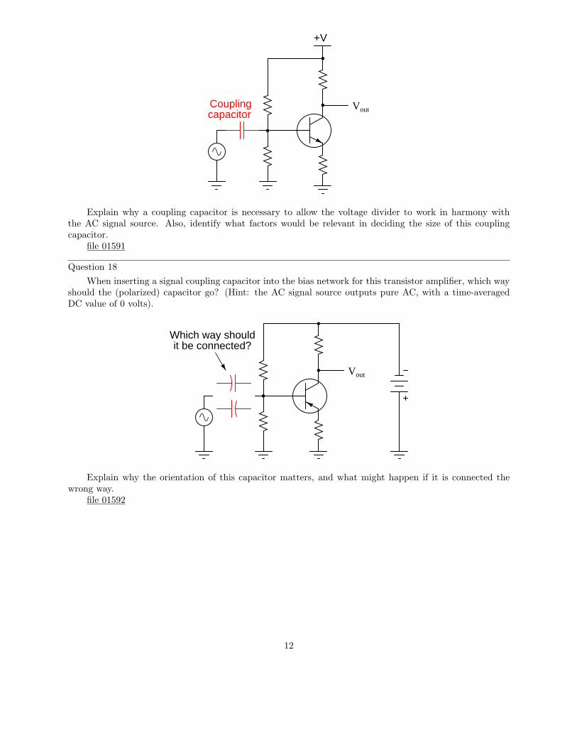
+V
VoutCouplingcapacitor
Explain why a coupling capacitor is necessary to allow the voltage divider to work in harmony withthe AC signal source. Also, identify what factors would be relevant in deciding the size of this couplingcapacitor.
file 01591
Question 18
When inserting a signal coupling capacitor into the bias network for this transistor amplifier, which wayshould the (polarized) capacitor go? (Hint: the AC signal source outputs pure AC, with a time-averagedDC value of 0 volts).
Vout
Which way shouldit be connected?
Explain why the orientation of this capacitor matters, and what might happen if it is connected thewrong way.
file 01592
12
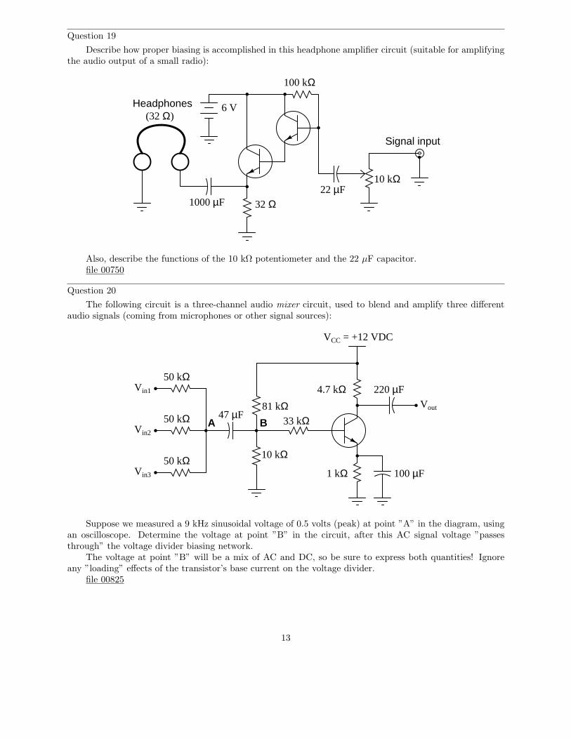
Question 19
Describe how proper biasing is accomplished in this headphone amplifier circuit (suitable for amplifyingthe audio output of a small radio):
Headphones
Signal input
1000 µF22 µF
6 V
32 Ω
100 kΩ
10 kΩ
(32 Ω)
Also, describe the functions of the 10 kΩ potentiometer and the 22 µF capacitor.file 00750
Question 20
The following circuit is a three-channel audio mixer circuit, used to blend and amplify three differentaudio signals (coming from microphones or other signal sources):
1 kΩ
10 kΩ
81 kΩ
Vin1
Vin2
Vin3
50 kΩ
50 kΩ
50 kΩ
47 µF
100 µF
220 µF
Vout
A 33 kΩ
4.7 kΩ
B
VCC = +12 VDC
Suppose we measured a 9 kHz sinusoidal voltage of 0.5 volts (peak) at point ”A” in the diagram, usingan oscilloscope. Determine the voltage at point ”B” in the circuit, after this AC signal voltage ”passesthrough” the voltage divider biasing network.
The voltage at point ”B” will be a mix of AC and DC, so be sure to express both quantities! Ignoreany ”loading” effects of the transistor’s base current on the voltage divider.
file 00825
13
Question 21
Don’t just sit there! Build something!!
Learning to mathematically analyze circuits requires much study and practice. Typically, studentspractice by working through lots of sample problems and checking their answers against those provided bythe textbook or the instructor. While this is good, there is a much better way.
You will learn much more by actually building and analyzing real circuits, letting your test equipmentprovide the ”answers” instead of a book or another person. For successful circuit-building exercises, followthese steps:
1. Carefully measure and record all component values prior to circuit construction, choosing resistor valueshigh enough to make damage to any active components unlikely.
2. Draw the schematic diagram for the circuit to be analyzed.3. Carefully build this circuit on a breadboard or other convenient medium.4. Check the accuracy of the circuit’s construction, following each wire to each connection point, and
verifying these elements one-by-one on the diagram.5. Mathematically analyze the circuit, solving for all voltage and current values.6. Carefully measure all voltages and currents, to verify the accuracy of your analysis.7. If there are any substantial errors (greater than a few percent), carefully check your circuit’s construction
against the diagram, then carefully re-calculate the values and re-measure.
When students are first learning about semiconductor devices, and are most likely to damage themby making improper connections in their circuits, I recommend they experiment with large, high-wattagecomponents (1N4001 rectifying diodes, TO-220 or TO-3 case power transistors, etc.), and using dry-cellbattery power sources rather than a benchtop power supply. This decreases the likelihood of componentdamage.
As usual, avoid very high and very low resistor values, to avoid measurement errors caused by meter”loading” (on the high end) and to avoid transistor burnout (on the low end). I recommend resistors between1 kΩ and 100 kΩ.
One way you can save time and reduce the possibility of error is to begin with a very simple circuit andincrementally add components to increase its complexity after each analysis, rather than building a wholenew circuit for each practice problem. Another time-saving technique is to re-use the same components in avariety of different circuit configurations. This way, you won’t have to measure any component’s value morethan once.
file 00505
14
Answers
Answer 1
Vout will increase, from 0 volts to approximately 9.3 volts (assuming a silicon transistor with a nominalbase-emitter voltage drop of 0.7 volts), as the potentiometer wiper is moved closer to +V.
Follow-up question: based on this result, would you be inclined to call this amplifier an inverting or anoninverting circuit?
Answer 2
Vin Vout
0.0 V 0.0 V0.5 V 0.0 V1.0 V 0.3 V1.5 V 0.8 V5.0 V 4.3 V7.8 V 7.1 V
The voltage at the transistor’s emitter terminal approximately ”follows” the voltage applied to the baseterminal, hence the name.
Answer 3
Trick question! Vout will remain at 0 volts the entire time.
Answer 4
Transistors are essentially DC devices, not AC devices. Consider the base-emitter PN junction that theinput signal is sent to: it can only conduct in one direction (base positive and emitter negative).
Answer 5
”Class-A” amplifier operation means that the final (power) transistor duplicates the entire waveshapeof the input signal, and not just a part of it.
Answer 6
”Class A” amplifier operation is when the transistor remains in its ”active” mode (conducting current)throughout the entire waveform. Biasing may be thought of as a kind of ”trick” used to get the transistor(a DC device) to ”think” it is amplifying DC when the input signal is really AC.
Answer 7
Vout will decrease, from +10 volts to nearly zero volts, as the potentiometer wiper is moved closer to+V.
Follow-up question: based on this result, would you be inclined to call this amplifier an inverting or anoninverting circuit?
Answer 8
Transistors are essentially DC devices, not AC devices. Consider the base-emitter PN junction that theinput signal is sent to: it can only conduct in one direction (base positive and emitter negative).
15
Answer 9
”Class A” amplifier operation is when the transistor remains in its ”active” mode (conducting current)throughout the entire waveform. Biasing may be thought of as a kind of ”trick” used to get the transistor(a DC device) to ”think” it is amplifying DC when the input signal is really AC.
Answer 10
The DC bias voltage (Vbias) is excessive.
Answer 11
Set the signal generator to ”sine-wave,” and the aural difference between a pure sine wave and a distorted(”clipped”) sine wave will be very apparent.
Answer 12
If the DC bias voltage shifts far enough away from the normal (quiescent) levels, the transistor may beforced into saturation or cutoff so it cannot reproduce the AC signal.
Answer 13
IB = 38.3 µA
Answer 14
At the threshold between cutoff and active mode, Vbias = -0.7 volts
At the threshold between active mode and saturation, Vbias = -1.72 volts (assuming 0 volts VCE atsaturation)
Follow-up question: if we were using the potentiometer to establish a bias voltage for an AC signal,what amount of DC bias voltage would place the transistor directly between these two extremes of operation(cutoff versus saturation), so as to allow the AC input signal to ”swing” equal amounts positive and negativeat the distortion limit? In other words, what voltage setting is exactly between -0.7 volts and -1.72 volts?
Answer 15
The purpose of any biasing network in an AC signal amplifier is to provide just enough quiescent currentthrough the base to keep the transistor between the extremes of cutoff and saturation throughout the inputsignal’s waveform cycle.
Answer 16
The purpose of any biasing network in an AC signal amplifier is to provide just enough quiescent currentthrough the base to keep the transistor between the extremes of cutoff and saturation throughout the inputsignal’s waveform cycle.
16
Answer 17
A very good way to understand the AC source’s effect on the voltage divider with and without thecapacitor is to use Superposition Theorem to determine what each source (AC signal, and DC power supply)will do separately.
If this concept is still not clear, consider this circuit:
Vin Vbias
Determine the voltageat this point
As far as capacitor size is concerned, it should be large enough that its reactance is negligible. I’ll letyou determine what factors define negligibility in this context!
Follow-up question: which voltage source (AC or DC?) ”wins” at the point specified in the above circuit?Explain why this is so, and then show how a suitably located capacitor would allow both voltage signals toco-exist at that point.
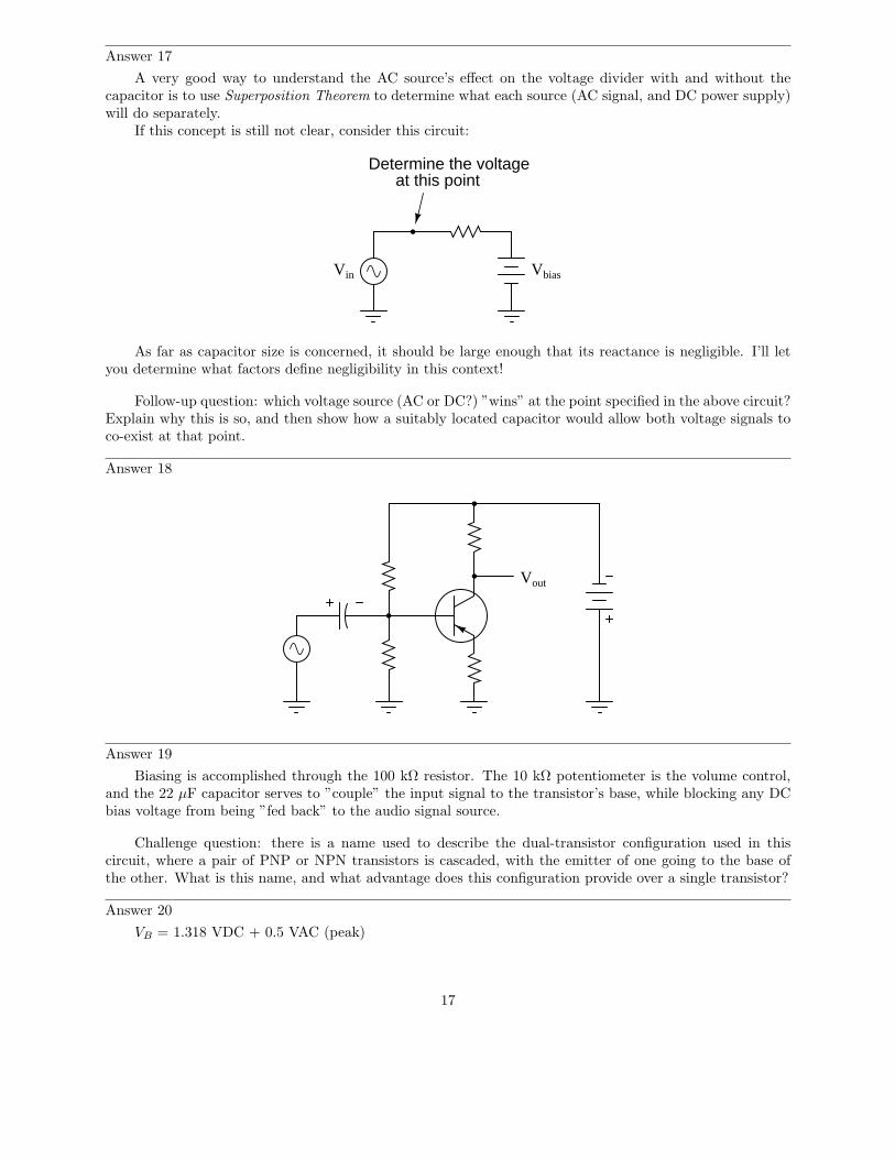
Answer 18
Vout
Answer 19
Biasing is accomplished through the 100 kΩ resistor. The 10 kΩ potentiometer is the volume control,and the 22 µF capacitor serves to ”couple” the input signal to the transistor’s base, while blocking any DCbias voltage from being ”fed back” to the audio signal source.
Challenge question: there is a name used to describe the dual-transistor configuration used in thiscircuit, where a pair of PNP or NPN transistors is cascaded, with the emitter of one going to the base ofthe other. What is this name, and what advantage does this configuration provide over a single transistor?
Answer 20
VB = 1.318 VDC + 0.5 VAC (peak)
17

Answer 21
Let the electrons themselves give you the answers to your own ”practice problems”!
18
Notes
Notes 1
Although this circuit is very simple, it is also very important to master. Be sure to discuss its operationthoroughly with your students, so they understand.
Notes 2
At first, the ”emitter follower” transistor circuit may seem pointless, since the output voltage practicallyequals the input voltage (especially for input voltages greatly exceeding 0.7 volts DC). ”What possible goodis a circuit like this?” some of your students may ask. The answer to this question, of course, has to do withcurrents in the circuit, and not necessarily voltages.
Notes 3
This might not be the result many students expect! It is important, though, for them to understandthe importance of polarity in transistor circuits. This example should make that abundantly clear.
Notes 4
Sometimes it is helpful for students to re-draw the circuit using a transistor model showing the base-emitter junction as a diode. If you think this model would help some of your students understand theconcept here, have another student draw the transistor model on the whiteboard, and use that drawing as adiscussion aid. Like any PN junction, the base-emitter junction of a BJT only ”wants” to conduct currentin one direction.
Notes 5
Of course, the natural question following this one is, ”What other classes of operation are there?” Thiswould be an excellent time to preview Class-B (push-pull) and Class-C operations if time permits.
Notes 6
A ”trick” it may be, but a very useful and very common ”trick” it is! Discuss this concept with yourstudents at length, being sure they have ample time and opportunity to ask questions of their own.
One question that may arise is, ”how much DC bias voltage is necessary?” If no one asks this question,ask it yourself! Discuss with your students what would constitute the minimum amount of bias voltagenecessary to ensure the transistor never goes into ”cutoff” anywhere in the waveform’s cycle, and also themaximum bias voltage to prevent the transistor from ”saturating”.
Notes 7
Although this circuit is very simple, it is also very important to master. Be sure to discuss its operationthoroughly with your students, so they understand.
Notes 8
Sometimes it is helpful for students to re-draw the circuit using a transistor model showing the base-emitter junction as a diode. If you think this model would help some of your students understand theconcept here, have another student draw the transistor model on the whiteboard, and use that drawing as adiscussion aid. Like any PN junction, the base-emitter junction of a BJT only ”wants” to conduct currentin one direction.
19
Notes 9
A ”trick” it may be, but a very useful and very common ”trick” it is! Discuss this concept with yourstudents at length, being sure they have ample time and opportunity to ask questions of their own.
One question that may arise is, ”how much DC bias voltage is necessary?” If no one asks this question,ask it yourself! Discuss with your students what would constitute the minimum amount of bias voltagenecessary to ensure the transistor never goes into ”cutoff” anywhere in the waveform’s cycle, and also themaximum bias voltage to prevent the transistor from ”saturating”.
Notes 10
Ask your students how they can tell the difference between excessive biasing and insufficient biasing, byinspection of the output waveform. There is a difference to be seen, but it requires a good understanding ofhow the circuit works! Students may be tempted to simply memorize waveforms (”when I see this kind ofwaveform, I know the problem is excessive biasing . . .”), so prepare to challenge their understanding withquestions such as:
• What polarity of input signal drives the transistor toward cutoff?• What polarity of input signal drives the transistor toward saturation?• Where on the output waveform is the transistor in cutoff (if at all)?• Where on the output waveform is the transistor in saturation (if at all)?• Where on the output waveform is the transistor in its active mode?
Another point worth mentioning: some students may be confused by the phasing of the input andoutput waveforms, comparing the two different oscilloscope displays. For a common-emitter (inverting)amplifier such as this, they expect to see the output voltage peak positive whenever the input voltage peaksnegative, and visa-versa, but here the two oscilloscope displays show positive peaks occurring right next tothe left-hand side of the screen. Why is this? Because the oscilloscope does not represent phase unless it isin dual-trace mode! When you disconnect the input probe and move it to another point in the circuit, anytime reference is lost, the oscilloscope’s triggering function placing the first waveform peak right where youtell it to, usually near the left-hand side of the display.
Notes 11
The answer I want for this question is not just a parroting of the answer I’ve given. Anyone can say ”adistorted wave will sound different.” I want to know how it sounds different, and this answer can only comeby direct experimentation!
Notes 12
This question asks students to explore the possibility of complete AC signal failure due to a simple shiftin DC bias, based on their understanding of how transistor amplifiers function. It may seem paradoxicalthat such a ”small” fault could have such a large effect on an amplifier circuit, but it should make sense oncestudents grasp how important bias is to class-A amplifier operation.
Notes 13
This circuit was purposely drawn in a convoluted fashion to force students to identify its configurationapart from the standard layout. Many people lack the spatial reasoning skills to do this easily, and requirea lot of practice before they become proficient. Ask your more proficient students if they have any ”tips”for helping those who struggle with problems like these. Are there any simple methods which we may useto re-draw this circuit in an easier-to-understand form?
20
Notes 14
If your students are experiencing difficulty analyzing this circuit, ask them to begin by calculating thetransistor currents at the thresholds of cutoff and saturation.
A mathematical trick I’ve found helpful through the years for finding the midpoint between two valuesis to add the two values together and then divide by two. Challenge your students to use other means ofcalculating this midpoint value, though.
Notes 15
All three biasing techniques are commonly used in transistor amplifier circuitry, so it behooves eachstudent to understand them well. In each case, resistors provide a ”trickle” of current through the base ofthe transistor to keep it turned partially ”on” at all times.
One exercise you might have your students do is come up to the board in front of the room anddraw an example of this circuit, then everyone may refer to the drawn image when discussing the circuit’scharacteristics.
Notes 16
All three biasing techniques are commonly used in transistor amplifier circuitry, so it behooves eachstudent to understand them well. In each case, resistors provide a ”trickle” of current through the base ofthe transistor to keep it turned partially ”on” at all times.
Notes 17
Many beginning students experience difficulty understanding the purpose of the coupling capacitor, andtransistor amplifier biasing in general. Be sure to spend plenty of time discussing the principle of this circuit,because it is very commonplace in transistor circuitry.
Notes 18
It is easy to miss the detail of the power supply’s polarity being ”backward” from what is typically seen(negative instead of positive). Actually, I am surprised to see how many introductory textbooks have thecoupling capacitor drawn the wrong way, so expect that some students may become confused by researchingtheir texts for the answer!
Notes 19
This circuit is simple enough to assemble and test in an hour or two, on a solderless breadboard. Itwould make a great lab experiment, and can be used by the students outside of class!
Notes 20
Ask your students what purpose the 47 µF capacitor serves. Since its presence does not noticeablyattenuate the AC signal at point ”A” (the whole 0.5 volts AC getting to point B), why not just replace itwith a straight piece of wire?
21
Notes 21
It has been my experience that students require much practice with circuit analysis to become proficient.To this end, instructors usually provide their students with lots of practice problems to work through, andprovide answers for students to check their work against. While this approach makes students proficient incircuit theory, it fails to fully educate them.
Students don’t just need mathematical practice. They also need real, hands-on practice building circuitsand using test equipment. So, I suggest the following alternative approach: students should build theirown ”practice problems” with real components, and try to mathematically predict the various voltage andcurrent values. This way, the mathematical theory ”comes alive,” and students gain practical proficiencythey wouldn’t gain merely by solving equations.
Another reason for following this method of practice is to teach students scientific method: the processof testing a hypothesis (in this case, mathematical predictions) by performing a real experiment. Studentswill also develop real troubleshooting skills as they occasionally make circuit construction errors.
Spend a few moments of time with your class to review some of the ”rules” for building circuits beforethey begin. Discuss these issues with your students in the same Socratic manner you would normally discussthe worksheet questions, rather than simply telling them what they should and should not do. I nevercease to be amazed at how poorly students grasp instructions when presented in a typical lecture (instructormonologue) format!
A note to those instructors who may complain about the ”wasted” time required to have students buildreal circuits instead of just mathematically analyzing theoretical circuits:
What is the purpose of students taking your course?
If your students will be working with real circuits, then they should learn on real circuits wheneverpossible. If your goal is to educate theoretical physicists, then stick with abstract analysis, by all means!But most of us plan for our students to do something in the real world with the education we give them.The ”wasted” time spent building real circuits will pay huge dividends when it comes time for them to applytheir knowledge to practical problems.
Furthermore, having students build their own practice problems teaches them how to perform primary
research, thus empowering them to continue their electrical/electronics education autonomously.In most sciences, realistic experiments are much more difficult and expensive to set up than electrical
circuits. Nuclear physics, biology, geology, and chemistry professors would just love to be able to have theirstudents apply advanced mathematics to real experiments posing no safety hazard and costing less than atextbook. They can’t, but you can. Exploit the convenience inherent to your science, and get those students
of yours practicing their math on lots of real circuits!
22