bjt fixed bias
DESCRIPTION
BJT Fixed Bias. ELEC 121. BJT Biasing 1. For Fixed Bias Configuration: Draw Equivalent Input circuit Draw Equivalent Output circuit Write necessary KVL and KCL Equations Determine the Quiescent Operating Point Graphical Solution using Loadlines Computational Analysis - PowerPoint PPT PresentationTRANSCRIPT
BJT Fixed Bias
ELEC 121
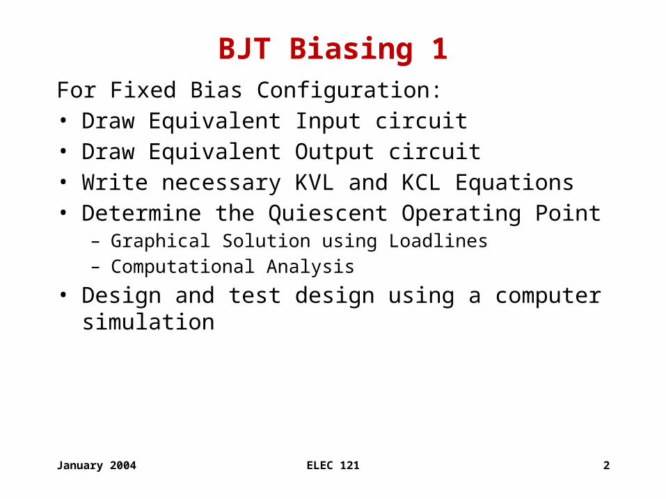
January 2004 ELEC 121 2
BJT Biasing 1For Fixed Bias Configuration:• Draw Equivalent Input circuit• Draw Equivalent Output circuit• Write necessary KVL and KCL Equations• Determine the Quiescent Operating Point
– Graphical Solution using Loadlines– Computational Analysis
• Design and test design using a computer simulation

January 2004 ELEC 121 3
Complete CE Amplifier with Fixed Bias

January 2004 ELEC 121 4
Fixed Bias and Equivalent DC Circuit
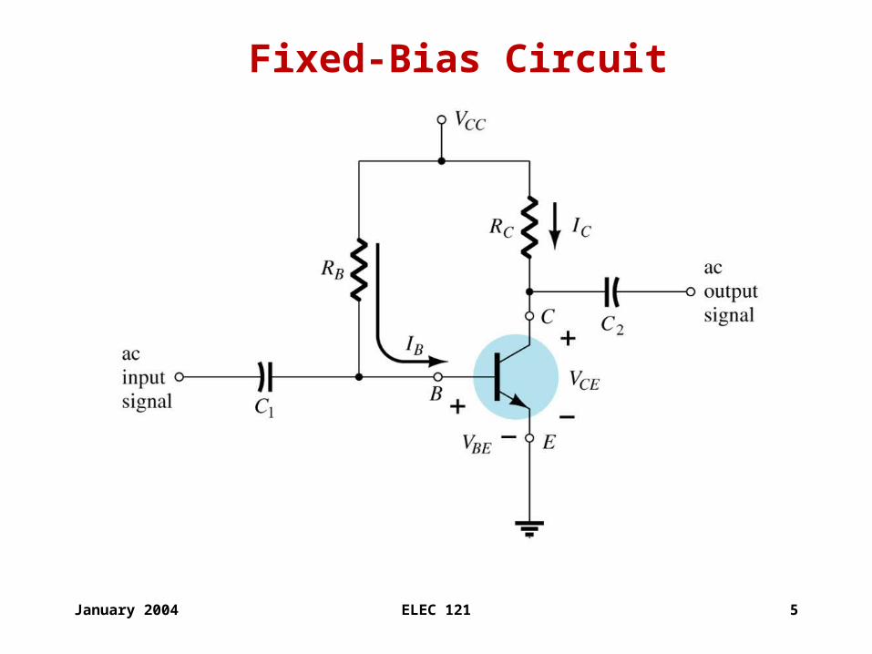
January 2004 ELEC 121 5
Fixed-Bias Circuit

January 2004 ELEC 121 6
DC Equivalent Circuit

January 2004 ELEC 121 7
Base-Emitter (Input) Loop
Using Kirchoff’s voltage law: – VCC + IBRB + VBE = 0
Solving for IB: CC BE
B B
V - VI =
R
January 2004 ELEC 121 8
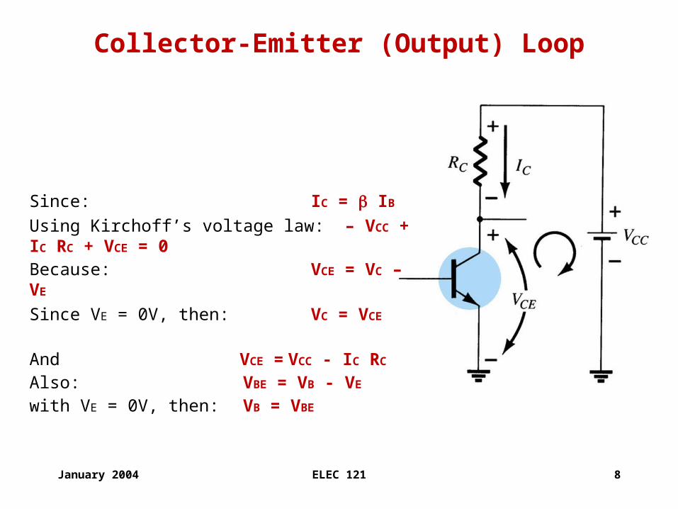
Collector-Emitter (Output) Loop
Since: IC = IB
Using Kirchoff’s voltage law: – VCC + IC RC + VCE = 0Because: VCE = VC – VE
Since VE = 0V, then: VC = VCE
And VCE = VCC - IC RC Also: VBE = VB - VE
with VE = 0V, then: VB = VBE

January 2004 ELEC 121 9
BJT Saturation Regions
When the transistor is operating in the Saturation Region, the transistor is conducting at maximum collector current (based on the resistances in the output circuit, not the spec sheet value) such that:
CC CE Csat
C
CEwhere
V - VI =
RV = 0 .2 V

January 2004 ELEC 121 10
Determining Icsat

January 2004 ELEC 121 11
Determining ICSAT for the fixed-bias configuration

January 2004 ELEC 121 12
Load Line Analysis

January 2004 ELEC 121 13
Load Line AnalysisThe end points of the line are : ICsat and VCEcutoffFor load line analysis, use VCE = 0 for ICSAT, and IC = 0 for VCEcutoff
ICsat:
VCEcutoff:
Where IB intersects with the load line we have the Q pointQ-point is the particular operating point: • Value of RB
• Sets the value of IB
• Where IB and Load Line intersect• Sets the values of VCE and IC.
CE
C
CC Csat V 0V
C
CE CC I 0mA
VI =
R
V = V
|
|
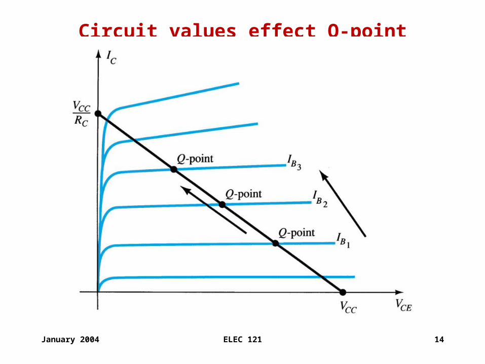
January 2004 ELEC 121 14
Circuit values effect Q-point

January 2004 ELEC 121 15
Circuit values effect Q-point (continued)

January 2004 ELEC 121 16
Circuit values effect Q-point (continued)

January 2004 ELEC 121 17
Load-line analysis
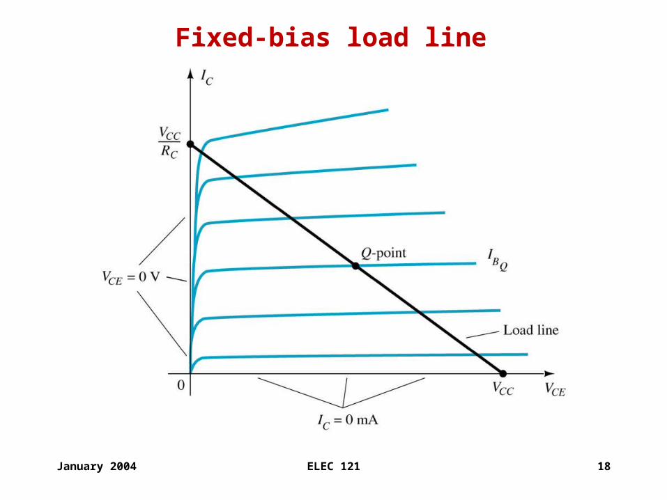
January 2004 ELEC 121 18
Fixed-bias load line

January 2004 ELEC 121 19
Example

January 2004 ELEC 121 20
DC Fixed Bias Circuit Example

January 2004 ELEC 121 21
Loadline Example Family of Curves