bl microcontrollers strategy deep-dive seminar presentations... · –upwards compatibility to...
TRANSCRIPT

LPC800 LPC Go Family
Mark Swinburn
BL Microcontrollers
September 2013

2
Agenda LPC800 Introduction
Cortex-M0+ Introduction
LPC800 Technical Introduction – GPIO
– Switch Matrix
– SCT
– Pattern Match Engine
– Analog Comparator
– Flexible GPIO
LPC800 Tools and Support
3
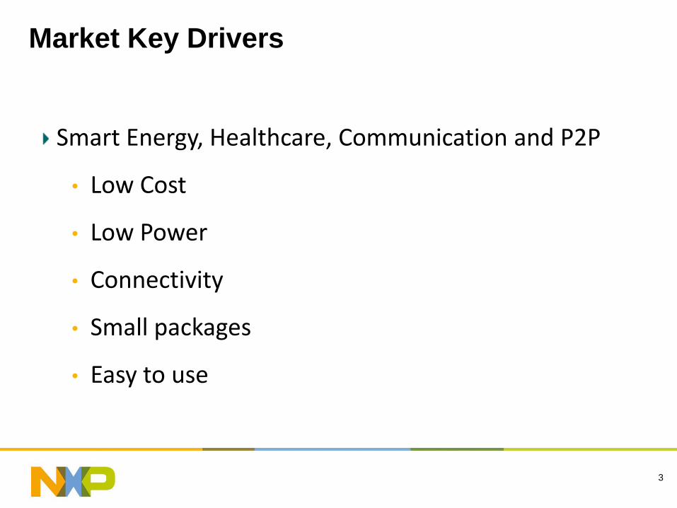
Market Key Drivers
Smart Energy, Healthcare, Communication and P2P
• Low Cost
• Low Power
• Connectivity
• Small packages
• Easy to use

4
The Newest Member of LPC Go Family F
LA
SH
PINS 16 20 24 33 48 64 80 100 144 180 208 256
Flashless
1MB
768kB
512kB
256kB
128kB
64kB
32kB
16kB
8kB
4kB
LPC Go
Ultra low power, low cost,
simple, easy to use
• Ultra fast TTM
• Designed for scalability
• Up to 50 MHz
• Flexible peripherals: switch matrix, SCT
• Serial I/O: UART, I2C
LPC Connect
Wide range of connectivity options,
from basic to advanced, including
high-precision analog features
•On-chip ROM drivers
• One to multiple, simultaneous communication protocols
• Range of package and memory options
•Pin-compatibility options for higher performance
• 72 to 120 MHz performance
• Connectivity peripherals: USB, CAN , Ethernet, LCD, more
High-performance, multi-connectivity,
advanced peripherals
• Display support
• Bandwidth and advanced peripherals for
tackling complex design challenges
• Up to 204 MHz
• HS USB + LCD + CAN + Ethernet + DSP instr.
LPC Turbo

5
Introducing the LPC800
8-bit Simplicity
32-bit Versatility
Smart Peripherals – Switch matrix
– State Configuration Timer
(SCT)
– Pattern Match Engine

6
LPC800 Cortex-M0+ Microcontrollers
Cortex-M0+ processor, up to 30MHz
Memory: – Up to 16 KB Flash
– Up to 4 KB SRAM
– USART, I2C, and Power Profile ROM Drivers
Peripherals: – Up to 3x USART, 2x SPI, 1x I2C
– 1x Analog Comparator, external Vref
– 4-ch Multi-Rate Timer, Self wake-up Timer
– Switch matrix for peripheral configurations
– State Configurable Timer, WatchDog Timer
– Pattern matching engine (GPIO)
– Up to 18 GPIO
– 1% accuracy, 12 MHz IRC oscillator
Single VDD power supply (1.8V to 3.6V)
TSSOP16/20, SO20 and DIP8
7
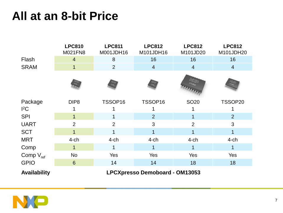
All at an 8-bit Price
LPC810
M021FN8
LPC811
M001JDH16
LPC812
M101JDH16
LPC812
M101JD20
LPC812
M101JDH20
Flash 4 8 16 16 16
SRAM 1 2 4 4 4
Package
DIP8 TSSOP16 TSSOP16 SO20 TSSOP20
I2C 1 1 1 1 1
SPI 1 1 2 1 2
UART 2 2 3 2 3
SCT 1 1 1 1 1
MRT 4-ch 4-ch 4-ch 4-ch 4-ch
Comp 1 1 1 1 1
Comp Vref No Yes Yes Yes Yes
GPIO 6 14 14 18 18
Availability LPCXpresso Demoboard - OM13053

8
Cortex-M0+ Overview
Best energy efficiency – New 2-stage pipeline
– Optimized accesses to program memory
Wider design options – Fast I/O Interface for single cycle access
– Micro Trace Buffer (MTB) for faster debug
Compatible with Cortex-M
Architecture – Full backward compatibility with Cortex-M0
– Upwards compatibility to Cortex-M3 and
Cortex-M4
– Existing compiler and debug tools can be
reused
“The ARM Cortex™-M0+ processor is the most energy efficient ARM
processor available”
Cortex-M0+ is an addition to Cortex-M0 for entry-level 32-bit microcontrollers
9
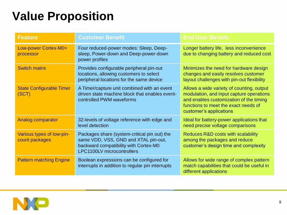
Value Proposition
Feature Customer Benefit End User Benefit
Low-power Cortex-M0+
processor
Four reduced-power modes: Sleep, Deep-
sleep, Power-down and Deep-power-down
power profiles
Longer battery life, less inconvenience
due to changing battery and reduced cost
Switch matrix Provides configurable peripheral pin-out
locations, allowing customers to select
peripheral locations for the same device
Minimizes the need for hardware design
changes and easily resolves customer
layout challenges with pin-out flexibility
State Configurable Timer
(SCT)
A Timer/capture unit combined with an event
driven state machine block that enables event-
controlled PWM waveforms
Allows a wide variety of counting, output
modulation, and input capture operations
and enables customization of the timing
functions to meet the exact needs of
customer’s applications
Analog comparator 32-levels of voltage reference with edge and
level detection
Ideal for battery-power applications that
need precise voltage comparisons
Various types of low-pin-
count packages
Packages share (system-critical pin out) the
same VDD, VSS, GND and XTAL pin-out,
backward compatibility with Cortex-M0
LPC1100LV microcontrollers
Reduces R&D costs with scalability
among the packages and reduce
customer’s design time and complexity
Pattern matching Engine Boolean expressions can be configured for
interrupts in addition to regular pin interrupts
Allows for wide range of complex pattern
match capabilities that could be useful in
different applications

10
LPC800 Overview

11
Memory Block Enhancements
Flash: 1K sectors with 64-byte page program/erase – EEPROM emulation
CRC Engine – Supports three common polynomials CRC-CCITT, CRC-16, and CRC-32
– Accept any size of data width per write: 8, 16 or 32-bit
On-chip BootROM drivers – Drivers for USART and I2C
– Power profiles for active run time power management
– In-System and In-Application Flash Programming Support

12
Enhanced Serial Interfaces
SPI speed
– Maximum data rates of 30 Mbit/s in
slave and master mode
I2C operation can be routed to: – Dedicated I2C pins (1Mbits/sec) and
– Any other open-drain pins (by routing the
functions using switch matrix)
– ROM drivers to configure I2C
USART – Synchronous operations on all 3 UARTs
– Maximum bit rates of 1.875 Mbit/s in
asynchronous mode and 30 Mbit/s in
synchronous mode for USART functions
– ROM drivers to configure USART
Wakeup from low power modes
13
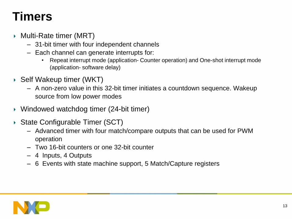
Timers
Multi-Rate timer (MRT) – 31-bit timer with four independent channels
– Each channel can generate interrupts for: • Repeat interrupt mode (application- Counter operation) and One-shot interrupt mode
(application- software delay)
Self Wakeup timer (WKT) – A non-zero value in this 32-bit timer initiates a countdown sequence. Wakeup
source from low power modes
Windowed watchdog timer (24-bit timer)
State Configurable Timer (SCT) – Advanced timer with four match/compare outputs that can be used for PWM
operation
– Two 16-bit counters or one 32-bit counter
– 4 Inputs, 4 Outputs
– 6 Events with state machine support, 5 Match/Capture registers

14
LPC800 Power Consumption
Active Deep
Sleep
100uA/MHz*
Below
170 uA
220 nA
Deep
Power Down
+ Power Profiles
Sleep
600 uA**
Power
Down
Below
1.8 uA
* while (1)
** 12 MHz, peripherals disabled
Low Power
Mode
Impact
Sleep
System Clock to Cortex-M0+ is stopped. Peripherals and memories are active. All enabled clocks are running. Processor state and registers, peripheral registers, and internal SRAM are maintained, and the logic levels of the pins remain static
Deep Sleep Peripherals receive no internal clocks. Flash is in stand-by mode. Processor state/registers, peripheral registers, and internal SRAM contents are maintained, and the logic levels of the pins remain static
Power Down Peripherals receive no internal clocks. The flash memory is powered down. Processor state/registers, peripheral registers, and internal SRAM contents are maintained, and the logic levels of the pins remain static
Deep Power
Down
The entire system is shut down except for five general purpose registers in the PMU and the self wake-up timer. Register states and internal SRAM contents are lost

15
Game Changing Peripherals!

16
Switch Matrix
Movable functions – Can be assigned to any external pin that is not power or ground
– UART, SPI, I2C, SCT, comparator o/p, CLKOUT, Pattern match o/p
Fixed pin functions – XTAL, comparator i/p, GPIOs
– Can be replaced by movable functions
Switch Matrix
UART
SPI
I2C
TIMER
P0_1
P0_2
P0_3
P0_4

17
State Configurable Timer (SCT)
Combines a 32-bit timer or 2 16-bit counters with
a configurable state machine – 4 Inputs, 4 Outputs
– 6 Events, 2 States, 5 Match/Capture registers
Implements virtually any timing or PWM function
found on popular 8-bit MCUs without loading the
CPU – Wide variety of counting, output, input, and
control operations
– Dead time insertion
– High resolution PWMs
GUI-based configuration tool (Redstate) – Integrated into LPCXpresso
– Choose pre-configured timing functions or build
your own
Custom control signals in
hardware:
• Clock or signal gating
• Complex modulation of outputs
• Pulse sequences
Motor Control
Generating PWM outputs,
triggering Comparator
Custom sampling of input
signals for:
• Frequency detection
• Pulse width detection
• Phase detection
Lighting
Modulated PWM outputs, reaction
to lamp sensor
18
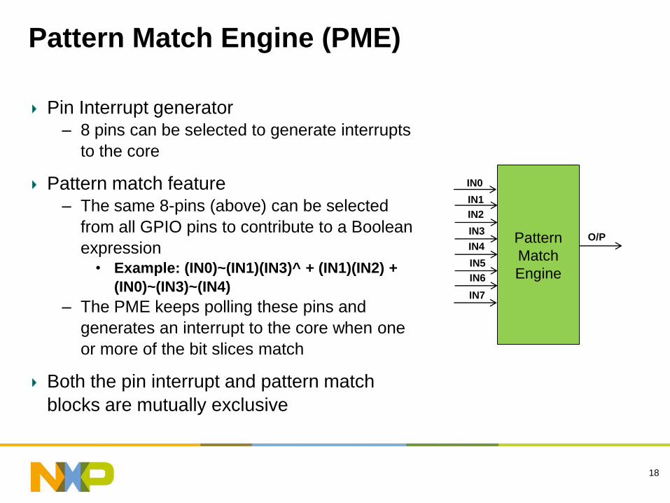
Pattern Match Engine (PME)
Pin Interrupt generator – 8 pins can be selected to generate interrupts
to the core
Pattern match feature – The same 8-pins (above) can be selected
from all GPIO pins to contribute to a Boolean
expression • Example: (IN0)~(IN1)(IN3)^ + (IN1)(IN2) +
(IN0)~(IN3)~(IN4)
– The PME keeps polling these pins and
generates an interrupt to the core when one
or more of the bit slices match
Both the pin interrupt and pattern match
blocks are mutually exclusive
Pattern
Match
Engine
IN0
IN1
IN2
IN3
IN4
IN5
IN6
IN7
O/P

19
LPC800 Comparator Block Diagram
1
9
0
31
LADSEL
LADEN & nACOMP_PD
1 0 LADREF
VDD pin VDDCMP pin
+
-
Vbandgap= 0.9V
IACMP_I1 pin IACMP_I2 pin
0
7
Vbandgap= 0.9V
IACMP_I1 pin IACMP_I2 pin
0
7
COM_VM_SEL
COM_VP_SEL
ACOMP_PD
HYS
COMPSTAT
COMPEDGE
(to interrupt)
SYNC
EDGE
DETECTION
1
0
ACMP_O pin
EDGESEL
ACOMP_RST_N
S
R
Q
EDGECLR
COMPSA
Voltage Ladder
Input Mux Analog Comparator
Output Mux

20
LPC800: Flexible I/O Port
I/O Port – Up to 18 GPIOs
– Single cycle access to all port pins
– Support high frequency I/O toggling – As fast as CPU_Clock/2 = 15MHz!
– Enhanced GPIO Pin Manipulation – Capable of simultaneously reading
Bit/Byte/Word or toggling up to 18 I/Os per instruction
– Bit-banding region
Application Advantages – High GPIO toggling frequency
– Bit-bang the I/O like an 8-bit!
– Reduced cycles

21
ROM Drivers for LPC800
On-chip ROM contains the boot loader and the following Application
Programming Interfaces (API):
– In-System Programming (ISP) and In-Application Programming
(IAP) support for flash programming
– USART driver API routines
• The UART API handles sending and receiving characters using
any of the USART blocks in asynchronous mode.
– I2C-bus driver API routines
• The drivers can be used to send or receive data on the I2C bus
in master and slave modes.
– Power profiles for optimizing power consumption and PLL settings

22
Easy-to-Use Packages

23
Low-Pin-Count Package Savings for Customers
Ease of Making Prototype – DIP or TSSOP for
prototyping on breadboard and hand-solder
Design
Ease of Assembly – Low-Pin-Count packages
for hand-solder during assembly
MFG
Reduced Manufacturing Process – No need
for reflow, no “QFN ground pad” to deal with,
and easy for re-work
Yield

24
Low-Pin-Count Package Options
Final Part Number SRAM Flash Package I2C SPI UART SCT MRT Comp Comp.
Vref GPIO
LPC810 M021FN8 1 4 DIP8 1 1 2 1 1, 4ch 1 No 6
LPC811 M001JDH16 2 8 TSSOP16 1
1 2 1 1, 4ch 1 Yes 14
LPC812 M101JDH16 4 16 TSSOP16 1
2 3 1 1, 4ch 1 Yes 14
LPC812 M10JFD20 4 16 SO20 1
1 2 1 1, 4ch 1 Yes 18
LPC812 M101JDH20 4 16 TSSOP20 1
2 3 1 1, 4ch 1 Yes 18
SO20 TSSOP20 TSSOP16 DIP8

25
Designed for Scalability
NXP’s low-pin-count
packages are designed for
sharing system-critical pin-out
Customers can easily swap
or scale packages that fit their
applications the most

26
Tool Support

27
LPCXpresso: NXP’s Low Cost Development Tool Platform
Eclipse-based IDE
Development Board
Evaluation Product Development

28
LPCXpresso (IDE + Evaluation Board + Emulator)
LPCXpresso board (OM#13053), MSRP: $29.95;
LPCXpreso IDE can be downloaded for free from www.nxp.com/lpcxpresso or
www.lpcware.com/lpcxpreso

29
LPCXpresso Development Stages
Evaluate
Explore
Develop

31
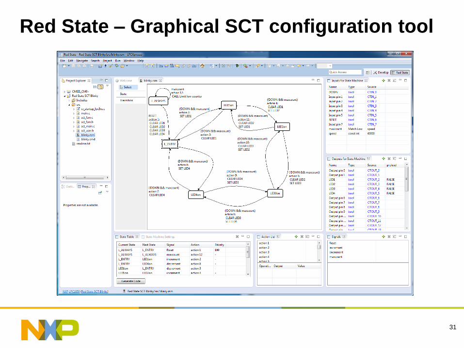
Red State – Graphical SCT configuration tool
32
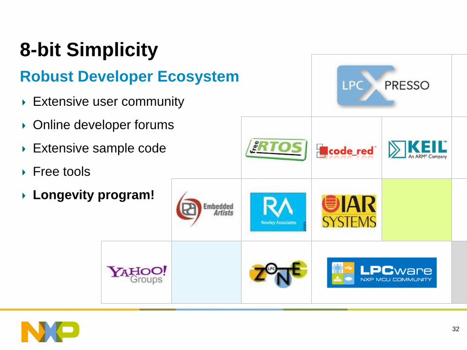
8-bit Simplicity
Robust Developer Ecosystem
Extensive user community
Online developer forums
Extensive sample code
Free tools
Longevity program!

33
Where to get started?
www.nxp.com/microcontrollers
– MCU homepage
www.nxp.com/lpczone
– Product updates and training
www.nxp.com/lpcxpresso – Low-cost development
www.lpcware.com – Engineering community

34
.... and finally
Ever increasing importance and reliance – Authentication
– Encryption
– Confidentiality
– Connectivity
Solution: – Hitex and NXP looking to hold NFC & Security seminars

35

36
Backup Slides

37
LPC800 Low Power Modes Low Power
Mode Impact Wake-Up Sources Current
Consumption
Sleep
System Clock to Cortex-M0+ is stopped. Peripherals and memories are active. All enabled clocks are running. Processor state and registers, peripheral registers, and internal SRAM are maintained, and the logic levels of the pins remain static
Any peripherals interrupts (SCT, MRT, USART, SPI, I2C, CMP) Pin interrupts & Pattern Match Engine BOD interrupt and reset WWDT interrupt and reset External Reset Self Wake-up Timer
600 µA *
Deep Sleep
Peripherals receive no internal clocks. Flash is in stand-by mode. Processor state/registers, peripheral registers, and internal SRAM contents are maintained, and the logic levels of the pins remain static
Interrupts from USART, SPI, I2C Pin interrupts BOD interrupt and reset WWDT interrupt and reset External Reset Self Wake-up Timer
170 µA
Power-Down
Peripherals receive no internal clocks. The flash memory is powered down. Processor state/registers, peripheral registers, and internal SRAM contents are maintained, and the logic levels of the pins remain static
Interrupts from USART, SPI, I2C Pin interrupts BOD interrupt and reset WWDT interrupt and reset External Reset Self Wake-up Timer
1.8 µA
Deep Power-
Down
The entire system is shut down except for five general purpose registers in the PMU and the self wake-up timer. Register states and internal SRAM contents are lost
Wake up on a pulse on the WAKEUP pin or when the self wake-up timer times out. On wake-up, the part reboots.
220 nA
* 12 MHz, peripherals disabled, low current mode

38
Cortex-M0+ Micro Trace Buffer (MTB)
CoreSight(TM) Micro Trace Buffer (MTB)
Trace store in RAM (non instrusive)
Read over Serial Wire / JTAG (CPU stopped)
For more details see
http://www.youtube.com/watch?v=gVz0efT7wO0&feature=plcp&list=PLgzOy9
g3ACxO6oD7Ltof_JW7-oeACChfl

39
Cortex-M0 vs. Cortex-M0+
Feature Cortex-M0 Cortex-M0+ Note
Architecture ARMv6-M ARMv6-M Binary compatible
Pipeline 3-stage 2-stage
Area (gate count) 12K 12K Approximately same area
Bus Interface AHB-Lite AHB-Lite I/O Port
Data access (cycles) 2 2 1 Fast I/O enabled
Privileged/ Unprivileged Privileged only Two levels
MPU option No Yes
Reloadable vector table No Yes
Multidrop debug support No Yes
Trace support No CoreSight MTB New basic program trace
Instruction fetch activity (Relative for Dhrystone)
1 0.85 Fewer flash accesses saves
energy
Performance efficiency 0.84 0.93
* 180nm ULL process using Artisan SC7 libraries, minimal configuration area for Cortex-M0 based on r0p0-03rel2