bl1100 - digi internationalftp1.digi.com/support/documentation/0190010e.pdf · power-supervisor...
TRANSCRIPT
BL1100C-Programmable Controller
User’s Manual019–0010 • 041015–E

Z-World, Inc.2900 Spafford StreetDavis, California 95616-6800USA
Telephone:Facsimile:Web Site:
E-Mail:
(530) 757-3737(530) 753-5141http://www.z w [email protected]
BL1100 User’s Manual
Part Number 019-0010 •
041015-E • Printed in U.S.A.
© 1999–2004 Z-World, Inc. •
All rights reserved.
Z-World reserves the right to make changes andimprovements to its products without providing notice.
Notice to UsersZ-WORLD PRODUCTS ARE NOT AUTHORIZED FOR USE AS CRITI-CAL COMPONENTS IN LIFE-SUPPORT DEVICES OR SYSTEMSUNLESS A SPECIFIC WRITTEN AGREEMENT REGARDING SUCHINTENDED USE IS ENTERED INTO BETWEEN THE CUSTOMERAND Z-WORLD PRIOR TO USE. Life-support devices or systems aredevices or systems intended for surgical implantation into the body or tosustain life, and whose failure to perform, when properly used in accor-dance with instructions for use provided in the labeling and user’s manual,can be reasonably expected to result in significant injury.
No complex software or hardware system is perfect. Bugs are always presentin a system of any size. In order to prevent danger to life or property, it is theresponsibility of the system designer to incorporate redundant protectivemechanisms appropriate to the risk involved.
Trademarks• Dynamic C
® is a registered trademark of Z-World
• Windows®
is a registered trademark of Microsoft Corporation
• PLCBus™
is a trademark of Z-World
• Hayes Smart Modem®
is a registered trademark of Hayes Microcom-puter Products, Inc.

Table of Contents iiiBL1100
TABLE OF CONTENTS
About This Manual ix
Chapter 1: Overview 13Overview .............................................................................................. 14Features ................................................................................................ 15Standard Models .................................................................................. 17
Options and Upgrades ..................................................................... 17Expansion Boards ........................................................................... 18
Development and Evaluation Tools ..................................................... 19Developer’s Kit ............................................................................... 19Software .......................................................................................... 19
Chapter 2: Getting Started 21Developer’s Kit Packing List ............................................................... 22Connecting BL1100 to a Host PC ........................................................ 22
Factory-Default RS-232 Programming ........................................... 22Establishing Communication with the BL1100 ................................... 24Running a Sample Program ................................................................. 24
Chapter 3: System Development 25Operating Modes ................................................................................. 26
Programming Options ..................................................................... 27Run Mode ........................................................................................ 30Switching Between Run and Program Mode .................................. 31
Memory ................................................................................................ 32EPROM ........................................................................................... 32
Programming EPROM.................................................................. 33SRAM ............................................................................................. 33
Chapter 4: Subystems 35Interface Overview............................................................................... 36Power-Supervisor Integrated Circuit ................................................... 37Digital Interfaces .................................................................................. 38
Zilog KIO Interface ......................................................................... 38KIO Command Register ............................................................... 39
iv Table of Contents BL1100
PIO Interface ................................................................................... 40Using PIO Ports ............................................................................ 42PIA Parallel Port ........................................................................... 44
Counter/Timer Circuit (CTC).......................................................... 44Timer Control Word ...................................................................... 46
High-Current/High-Voltage Driver ................................................. 48Liquid Crystal Display Interface ..................................................... 50
Serial Communication .......................................................................... 52RS-232 Communication .................................................................. 54
Modem Communication ............................................................... 54XMODEM File Transfer .............................................................. 54
RS-485 Communication .................................................................. 55Developing an RS-485 Network ................................................... 55Hardware Connection ................................................................... 56
Direct Programming Using Serial Ports ............................................... 57Attainable Baud Rates ..................................................................... 59Z180 Serial Ports ............................................................................ 60
Asynchronous Serial Communication Interface ................................... 62ASCI Status Registers ..................................................................... 62ASCI Control Register A ................................................................ 64ASCI Control Register B ................................................................ 65
SIO Serial Ports ................................................................................... 67Programming the SIO in Asynchronous Mode ............................... 70
Chapter 5: Analog Section 73Analog Inputs ....................................................................................... 74
Signal Conditioning ........................................................................ 74Configuration 4 .......................................................................... 75Configuration 5 .......................................................................... 75
Installing Components .................................................................... 76A/D Conversion ................................................................................... 84
Sources of Error .............................................................................. 84Onboard Temperature Sensor .......................................................... 85
Analog Output ...................................................................................... 87
Chapter 6: Software Reference 89Supplied Software ................................................................................ 90Digital Interfaces .................................................................................. 91
KIO Counter/Timer Circuit (CTC) ................................................. 91High-Current/High-Voltage Driver ................................................. 92Liquid Crystal Display Interface ..................................................... 93
A/D Converter ...................................................................................... 94Temperature Measurements .......................................................... 94
High-Speed Sampling ..................................................................... 95

Table of Contents vBL1100
D/A Converter ...................................................................................... 96Miscellaneous Drivers ......................................................................... 96
Time/Date Clock ............................................................................. 96Time/Date Functions ..................................................................... 96
Watchdog Timer .............................................................................. 97
Appendix A: Troubleshooting 99Out of the Box.................................................................................... 100Dynamic C Will Not Start .................................................................. 100Dynamic C Loses Serial Link ............................................................ 101BL1100 Repeatedly Resets ................................................................ 101PIO Problems ..................................................................................... 101Power-Supply Problems ..................................................................... 101Blown-Out 5841 Driver Chip ............................................................ 102Common Programming Errors ........................................................... 102
Appendix B: Specifications 103Electrical and Mechanical Specifications .......................................... 104
BL1100 Mechanical Dimensions .................................................. 105Jumper and Header Specifications ..................................................... 106
Wago Connector Signals ............................................................... 107LCD Interface ............................................................................... 108Serial Communication Signals ...................................................... 108PIO Parallel Port and Other Lines ................................................ 109BL1100 Expansion Bus ................................................................. 109Jumper Configurations .................................................................. 110
Appendix C: Memory, I/O Map, and Interrupt Vectors 113BL1100 Memory ................................................................................ 114
Physical Memory .......................................................................... 114Memory Management ................................................................... 114How Dynamic C Uses the MMU .................................................. 116Control over Memory Mapping .................................................... 118Extended Memory Code ............................................................... 118Extended Memory Data ................................................................ 119Execution Timing .......................................................................... 119Memory-Access Timing ................................................................ 120
Memory Map ..................................................................................... 122Time/Date Clock ................................................................................ 126
Initialized Memory Locations ....................................................... 127Interrupt Vectors ................................................................................ 127Nonmaskable Interrupts ..................................................................... 129
Power-Fail Interrupts .................................................................... 129
vi Table of Contents BL1100
Jump Vectors ...................................................................................... 130Interrupt Priorities .............................................................................. 131
Appendix D: EEPROM 133Parameters .......................................................................................... 134Library Routines ................................................................................ 135
Appendix E: Power Management 137Power Consumption ........................................................................... 138Intermittent Operation ........................................................................ 139
Appendix F: Opto 22 Support 141
Appendix G: Sample Analog Applications 149Semiconductor Temperature Sensor .................................................. 150Thermocouple .................................................................................... 1514–20 mA Loop ................................................................................... 152
Appendix H: PLCBus 153Overview ............................................................................................ 154Allocation of Devices on the Bus ...................................................... 158
4-Bit Devices ................................................................................ 1588-Bit Devices ................................................................................ 159
Expansion Bus Software .................................................................... 159
Appendix I: Simulated PLCBus Connection 165PIO Port Connections ........................................................................ 166
Standard Z-World Expansion Boards ............................................ 166Software Drivers ................................................................................ 167
Using Expansion Boards with PIO 1 Port A ................................. 167General-Purpose Drivers ............................................................ 167Relay Expansion Board Drivers ................................................. 168D/A Converter Expansion Board Drivers ................................... 169
Appendix J: Standalone Operation 171Reliability ........................................................................................... 173
Program Life ................................................................................. 173Speed ............................................................................................. 174Data Space .................................................................................... 174Cost ............................................................................................... 174Ease ............................................................................................... 174
Remote Downloading ........................................................................ 174
Table of Contents viiBL1100
Appendix K: BL1100 Expansion Boards 179Introduction ........................................................................................ 180Installation ......................................................................................... 180
Address Mapping for Multiple Cards ........................................... 182Subsystems ......................................................................................... 183
Digital I/O ..................................................................................... 185Programmable Peripheral Interface (PPI) ................................... 185
Port A ....................................................................................... 186Port B ....................................................................................... 186Port C ....................................................................................... 186
Operating Modes ........................................................................ 189Mode 0 ..................................................................................... 189Mode 1 ..................................................................................... 189Mode 2 ..................................................................................... 189
TTL Input Buffer ........................................................................ 189Pulse Width Measurement ............................................................. 190
Clocks ......................................................................................... 193Other Information ....................................................................... 193
Analog Multiplexer ....................................................................... 194Instrumentation Amplifier ............................................................. 195A/D Converter ............................................................................... 196DGL96 .......................................................................................... 199
Software ............................................................................................. 200IOEXPAND.LIB ........................................................................... 20096IO.LIB ....................................................................................... 205Sample Programs .......................................................................... 207
Pulse Width Measurement .......................................................... 207Other Sample Programs .............................................................. 209
PWM PAL Equations .................................................................... 210Board Layouts .................................................................................... 211I/O Map .............................................................................................. 216Jumper and Header Specifications ..................................................... 220
ADC, DGL, and MUX Expansion Board Signals ......................... 220DGL96 Expansion Board Signals ................................................. 221Jumper Configurations .................................................................. 222
Appendix L: Backup Battery 223Battery Life and Storage Conditions .................................................. 224Replacing Soldered Lithium Battery .................................................. 224Battery Cautions ................................................................................ 225
Index 227
Schematics

viii s Table of Contents BL1100
About This Manual ixBL1100
ABOUT THIS MANUAL
This manual provides instructions for installing, testing, configuring, andinterconnecting any of the Dynamic C programmable controllers in theBL1100 series. (The BL1100 was previously called the Little Giant.)The term “BL1100” will be used generically throughout this manual whenreferring to any controller in the BL1100 series. Where informationapplies to a specific controller, the model number will be specified.Models currently covered by this manual include the BL1100, BL1110,and BL1120.Instructions to get started using Dynamic C software programmingfunctions as well as complete C and Dynamic C references and program-ming resources are referenced when necessary.
AssumptionsAssumptions are made regarding the user's knowledge and experience inthe following areas:• Ability to design and engineer a target system that a BL1100 will
control.• Understanding of the basics of operating a software program and
editing files under Windows on a PC.• Knowledge of the basics of C programming.
For a full treatment of C, refer to the following texts.The C Programming Language by Kernighan and RitchieC: A Reference Manual by Harbison and Steel
• Knowledge of basic Z80 assembly language and architecture.For documentation from Zilog, refer to the following texts.Z180 MPU User's ManualZ180 Serial Communication ControllersZ80 Microprocessor Family User's Manual

BL1100x s About This Manual
AcronymsTable 1 lists and defines the acronyms that may be used in this manual.
IconsTable 2 displays and defines icons that may be used in this manual.
Table 2. Icons
Icon Meaning Icon Meaning
$ Refer to or see ! Note
( Please contact 7LS Tip
Caution High Voltage
)'
Factory Default
Table 1. Acronyms
Acronym Meaning
EPROM Erasable Programmable Read-Only Memory
EEPROM Electronically Erasable Programmable Read-Only Memory
LCD Liquid Crystal Display
LED Light-Emitting Diode
NMI Nonmaskable Interrupt
PIO Parallel Input/Output Circuit(Individually Programmable Input/Output)
PRT Programmable Reload Timer
RAM Random Access Memory
RTC Real-Time Clock
SIB Serial Interface Board
SRAM Static Random Access Memory
UART Universal Asynchronous Receiver Transmitter

About This Manual s xiBL1100
ConventionsTable 3 lists and defines the typographical conventions that may be used inthis manual.
Pin Number 1A black square indicatespin 1 of all headers.
MeasurementsAll diagram and graphic measurements are in inches followed by millime-ters enclosed in parenthesis.
Table 3. Typographical Conventions
Example Description
while Courier font (bold) indicates a program, a fragment of aprogram, or a Dynamic C keyword or phrase.
// IN-01… Program comments are written in Courier font, plain face.
Italics Indicates that something should be typed instead of theitalicized words (e.g., in place of filename, type a file’sname).
Edit Sans serif font (bold) signifies a menu or menu selection.
. . . An ellipsis indicates that (1) irrelevant program text isomitted for brevity or that (2) preceding program text maybe repeated indefinitely.
[ ] Brackets in a C function’s definition or program segmentindicate that the enclosed directive is optional.
< > Angle brackets occasionally enclose classes of terms.
a | b | c A vertical bar indicates that a choice should be made fromamong the items listed.
J1Pin 1

BL1100xii s About This Manual

BL1100 Overview 13
CHAPTER 1: OVERVIEW
BL110014 s Overview
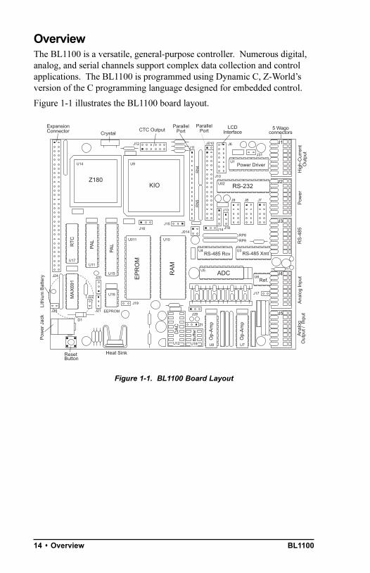
OverviewThe BL1100 is a versatile, general-purpose controller. Numerous digital,analog, and serial channels support complex data collection and controlapplications. The BL1100 is programmed using Dynamic C, Z-Worldsversion of the C programming language designed for embedded control.
Figure 1-1 illustrates the BL1100 board layout.
Figure 1-1. BL1100 Board Layout
EP
RO
M
RA
M
ExpansionConnector Crystal
CTC Output LCDInterface
Z180KIO
J12
J10
J6
J31
Power DriverU1
RS-232U02
J8 J7J9
J14
J13
J18J014
RP8RP9
RS-485 Xmt
U10
U3
ADCU5
Ref.U6
J17
Op-
Am
p
U8
Op-
Am
p
U7
U011
U9U14
J15J16
J19
J28
DA
C
U12
Buf
fer
U19
EEPROM
U16
U15
PAL
U11
PAL
U17
RT
C
U18
J22
J21
D1
J24
J25
ResetButton
J1
J2
J3
J4
J5
U4
RN
4R
N5
Pow
er J
ack
Heat Sink
Ana
log
Inpu
tA
nalo
gO
utpu
t / I
nput
RS
-485
Pow
erH
igh-
Cur
rent
Out
put
J010
Lith
ium
Bat
tery
MA
X69
1
J11
ParallelPort
ParallelPort 5 Wago
connectors
Z1
J20
RS-485 Rcv
BL1100 Overview s 15
FeaturesThe BL1100 includes the following features.
Compactnessdimensions of 5.6" × 4.8" (140 mm × 120 mm).
Serial channelstwo RS-232 and two RS-485/RS-422 serial ports.
Configurable I/O16 programmable TTL and CMOS compatible I/Olines based on the 16-bit PIO on the Zilog KIO chip.
High-current digital outputs8 high-current digital outputs based onthe Sprague 5841 driver. Channels can be paralleled for more current.The drivers are protected against inductive kickback with integraldiodes and are suitable for driving solenoids.
Analog inputseight-channel A/D converter with configurable inputs.A built-in temperature sensor uses one of the inputs, leaving sevenanalog inputs for use by the application. The A/D converter can have10-bit resolution (LTC1094) or 12-bit resolution (LTC1294).
Optional factory-installed analog output12-bit digital to analogconverter (DAC) with output in the range of 0 V to 2.5 V. The MaximAD7543 DAC is used with a MAX400 buffer amplifier for a maximumoutput of 2 mA.
LCD interfacestandard LCDs (such as Optrex part numberDMC20481) can be plugged directly into the 14-pin connector. Manycompatible displays are available in various formats (2 ×16 or 4 × 40).
Z180 microprocessor running at 9.216 MHz with a partial wait state.Higher clock rates are available for better performance.
Power failure detection and warning. A nonmaskable interrupt takesplace when power drops below a certain level. The program has a fewmilliseconds to shut down.
Watchdog timer. When enabled, the watchdog timer automaticallyresets the board if the watchdog timer system is not regularly hit bythe program. This reliability feature helps a system to recover fromsoftware or hardware failures.
32K EPROM, supports up to 256K. Accepts either 28- or 32-pin ROM.
32K battery-backed SRAM, supports up to 512K. Either 28- or 32-pinRAM can be used. The lithium battery mounted on the board will lastabout 10 years.
512 bytes of EEPROM. One-half of the EEPROM memory (256bytes) can be write-protected. EEPROM is used to hold the baud rateand other semipermanent calibration or setup constants. (Can beexpanded to 2048 bytes by using different components.)

BL110016 s Overview
Battery-backed Epson 72421 real-time clock runs up to 10 years on thelithium battery.
Both linear and switching power regulators are present on the board.
Enclosures are available from different suppliers in table-top plasticclamshell or wall-mounted industrial versions. For example, theHoffman Engineering Company (Anoka, Minn.) enclosure D-864DLBand mounting plate A-8P6 provide a sturdy steel electrical box. Thisbox can be wall mounted and connected to electrical conduit.
The analog inputs, analog output, power, RS-485, and high-currentoutputs are on Wago connectors that accept up to approximately #18copper wire. The Wago connectors have spring loaded clamps thatmake it easy to install and remove wires without special tools. Theentire BL1100 series is also available without Wago connectors so thatother connector types may be added instead.
A 60-pin expansion connector allows a line of expansion boardsdesigned exclusively for the BL1100 series to be connected to themicroprocessor bus. Selected standard Z-World expansion boards canalso be connected to the PIO header.
BL1100 Overview s 17
(
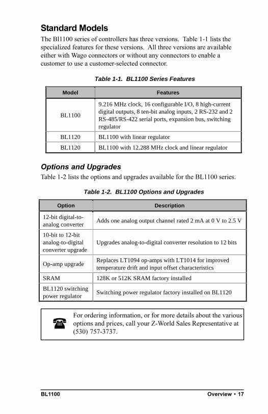
Table 1-1. BL1100 Series Features
Model Features
BL1100
9.216 MHz clock, 16 configurable I/O, 8 high-currentdigital outputs, 8 ten-bit analog inputs, 2 RS-232 and 2RS-485/RS-422 serial ports, expansion bus, switchingregulator
BL1120 BL1100 with linear regulator
BL1120 BL1100 with 12.288 MHz clock and linear regulator
Table 1-2. BL1100 Options and Upgrades
Option Description
12-bit digital-to-analog converter
Adds one analog output channel rated 2 mA at 0 V to 2.5 V
10-bit to 12-bitanalog-to-digitalconverter upgrade
Upgrades analog-to-digital converter resolution to 12 bits
Op-amp upgradeReplaces LT1094 op-amps with LT1014 for improvedtemperature drift and input offset characteristics
SRAM 128K or 512K SRAM factory installed
BL1120 switchingpower regulator
Switching power regulator factory installed on BL1120
Standard ModelsThe Bl1100 series of controllers has three versions. Table 1-1 lists thespecialized features for these versions. All three versions are availableeither with Wago connectors or without any connectors to enable acustomer to use a customer-selected connector.
Options and UpgradesTable 1-2 lists the options and upgrades available for the BL1100 series.
For ordering information, or for more details about the variousoptions and prices, call your Z-World Sales Representative at(530) 757-3737.
BL110018 s Overview
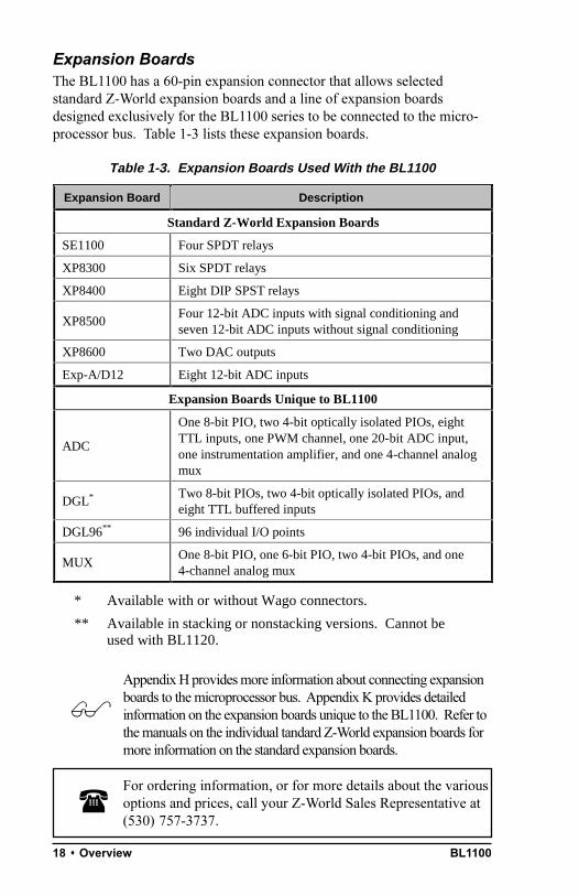
(
Table 1-3. Expansion Boards Used With the BL1100
Expansion Board Description
Standard Z-World Expansion Boards
SE1100 Four SPDT relays
XP8300 Six SPDT relays
XP8400 Eight DIP SPST relays
XP8500Four 12-bit ADC inputs with signal conditioning andseven 12-bit ADC inputs without signal conditioning
XP8600 Two DAC outputs
Exp-A/D12 Eight 12-bit ADC inputs
Expansion Boards Unique to BL1100
ADC
One 8-bit PIO, two 4-bit optically isolated PIOs, eightTTL inputs, one PWM channel, one 20-bit ADC input,one instrumentation amplifier, and one 4-channel analogmux
DGL* Two 8-bit PIOs, two 4-bit optically isolated PIOs, andeight TTL buffered inputs
DGL96** 96 individual I/O points
MUXOne 8-bit PIO, one 6-bit PIO, two 4-bit PIOs, and one4-channel analog mux
* Available with or without Wago connectors.
** Available in stacking or nonstacking versions. Cannot beused with BL1120.
Expansion BoardsThe BL1100 has a 60-pin expansion connector that allows selectedstandard Z-World expansion boards and a line of expansion boardsdesigned exclusively for the BL1100 series to be connected to the micro-processor bus. Table 1-3 lists these expansion boards.
Appendix H provides more information about connecting expansionboards to the microprocessor bus. Appendix K provides detailedinformation on the expansion boards unique to the BL1100. Refer tothe manuals on the individual tandard Z-World expansion boards formore information on the standard expansion boards.
For ordering information, or for more details about the variousoptions and prices, call your Z-World Sales Representative at(530) 757-3737.
$
BL1100 Overview s 19
Development and Evaluation ToolsThe BL1100 is supported by a Developers Kit that includes everythingyou need to start development with the BL1100.
Developers KitThe Developers Kit includes these items.
Manual with schematics.
Programming cables and adapter.
9 V DC power supply.
128K SRAM.
SoftwareThe BL1100 is programmed using Z-Worlds Dynamic C, an integrateddevelopment environment that includes an editor, a C compiler, and adebugger. Library functions provide an easy and robust interface to theBL1100.
Z-Worlds Dynamic C reference manuals provide completesoftware descriptions and programming instructions.$

BL110020 s Overview

BL1100 Getting Started 21
CHAPTER 2: GETTING STARTED
Chapter 2 provides instructions for connecting the BL1100 to a host PCand running a sample program.

BL110022 s Getting Started
Developers Kit Packing ListThe BL1100 Developers Kit includes the following items.
Serial cable with DB-9 and 10-pin header connectors.
DB-25 to DB-9 serial adapter.
9 V DC power transformer.
128K SRAM chip.
BL1100 Users Manual (this document).
Connecting BL1100 to a Host PCThe BL1100 can be programmed using a PC using either an RS-232 serialport or an RS-485 serial port.
See Chapter 3, System Development, for information onother programming configurations. Z-World recommendstrying out the factory-default configuration first to make surethat your setup works.
Factory-Default RS-232 Programming1. Make sure Dynamic C is installed on your PC as described in the
Dynamic C Technical Reference manual.
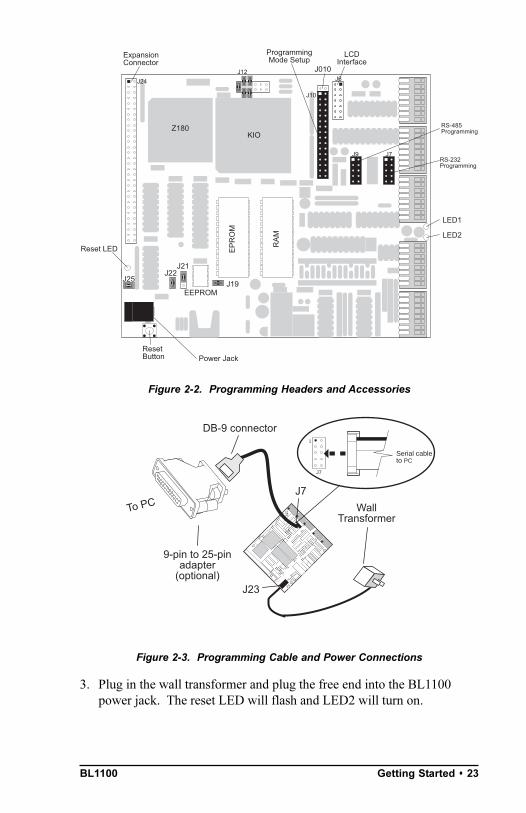
2. The BL1100 is factory configured for RS-232 programming at19,200 bps. Use the programming cable provided in the DevelopersKit (see Figure 2-1) to connect header J7 (shown in Figure 2-2) to thehost PC COM1 serial port as shown in Figure 2-3.
Figure 2-1. Programming Cable
12
3
9
To B
L1100
To host
PC5
196
$
BL1100 Getting Started s 23
Figure 2-2. Programming Headers and Accessories
Figure 2-3. Programming Cable and Power Connections
3. Plug in the wall transformer and plug the free end into the BL1100power jack. The reset LED will flash and LED2 will turn on.
EP
RO
M
RA
M
ExpansionConnector
LCDInterface
Z180KIO
J19EEPROM
U18
J22J21
ResetButton Power Jack
LED1
LED2
Reset LED
J10
J6
J9 J7RS-232Programming
RS-485Programming
J24
J12
J25
J010
ProgrammingMode Setup
Heat
J12
J11
J10
J6
J7
J8
J9
J1
J2
J3
J13
J23
RP6J18
J31
J30
J7
J23
To PC
DB-9 connector
WallTransformer
9-pin to 25-pinadapter
(optional)
Serial cableto PC
J7
1

BL110024 s Getting Started
Establishing Communication with the BL11001. Double-click the Dynamic C icon to start the software. Note that
communication with the BL1100 is attempted each time you startDynamic C.
2. If the communication attempt is successful, no error messages aredisplayed.
3. If the programming cable is connected to a port other than COM1, usethe Setup Target option in the SETUP menu <ALT S> in Dynamic C tospecify the correct port. You may need to reset the BL1100.
See Appendix A, Troubleshooting, if an error message suchas Target Not Responding or Communication Error appears.
Once the necessary changes have been made to establish com-munication between the host PC and the BL1100, use the Dy-namic C shortcut <Ctrl Y> to reset the controller and initiatecommunication.
Running a Sample Program1. Load the sample program LGFLASH.C located in the Dynamic C
SAMPLES directory using <ALT O>. This program flashes LED2.
2. Compile the program by pressing F3 or by choosing Compile from theCompile menu.
During compilation, Dynamic C rapidly displays several messages inthe compiling window. This condition is normal.
See Appendix A, Troubleshooting, if an error message suchas Target Not Responding or Communication Error appears.
3. Run the program by pressing F9 or by choosing Run from the RunMenu. You may also single step through the program using F7 and F8,and experiment with changing the delay times.
4. To halt the program, press <Ctrl Z>. This action halts programexecution.
5. To restart program execution, when required, press F9.
$
!
$

BL1100 System Development 25
CHAPTER 3: SYSTEM DEVELOPMENT
Chapter 3 describes the more advanced aspects of setting up and using theBL1100. The following sections are included.• Operating Modes• Memory
BL110026 s System Development
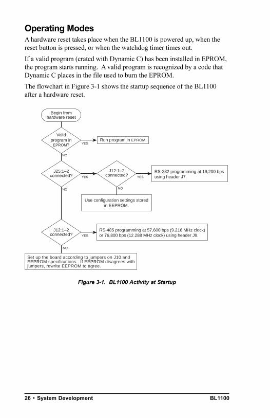
Operating ModesA hardware reset takes place when the BL1100 is powered up, when thereset button is pressed, or when the watchdog timer times out.
If a valid program (crated with Dynamic C) has been installed in EPROM,the program starts running. A valid program is recognized by a code thatDynamic C places in the file used to burn the EPROM.
The flowchart in Figure 3-1 shows the startup sequence of the BL1100after a hardware reset.
Figure 3-1. BL1100 Activity at Startup
Validprogram in
EPROM? YES
YES
YES
Set up the board according to jumpers on J10 andEEPROM specifications. If EEPROM disagrees withjumpers, rewrite EEPROM to agree.
Begin fromhardware reset
Run program in EPROM.
J25:1–2connected?
RS-232 programming at 19,200 bpsusing header J7.YES
J12:1–2connected?
Use configuration settings storedin EEPROM.
RS-485 programming at 57,600 bps (9.216 MHz clock)or 76,800 bps (12.288 MHz clock) using header J9.
J12:1–2connected?
NO
NO NO
NO

BL1100 System Development s 27
Programming OptionsIn addition to the RS-232 factory-default programming at 19,200 bps de-scribed in Chapter 2, Getting Started, the BL1100 may be programmedusing RS-485/RS-422, and programming is also possible using either RS-232or RS-485/RS-422 at different baud rates. Figure 3-2 shows the variousprogramming modes and jumper configurations for headers J12 and J25.
Figure 3-2. Jumper Configurations for Programming Options
Follow these steps for the alternative programming options.
1. Make sure Dynamic C is installed on your PC as described in theDynamic C Technical Reference manual.
2. Plug the free end of the power supplyinto the BL1100 power jack as shownin Figure 3-3.
Do not plug the transformerinto the wall until all the con-nections and jumpers havebeen set on the BL1100.
3. Set the jumpers on header J25 and onheader J12 pins 12.
Option 1 (RS-232 at 19,200 bps)This factory-default option was de-scribed in Chapter 2, Getting Started. No changes to the factory jumpersettings are needed.
Option 2 (RS-485 at 57,600 bps)Remove the jumper from header J25as shown in Figure 2-4. This option allows RS-485/RS-422 program-ming at 57,600 bps (BL1100, BL1110) or 76,800 bps (BL1120). Go tostep 4.
Option 3 (store and use settings inEEPROM)Move the jumper onheader J21 to pins 23 as shown in Fig-ure 3-4 to write-enable the EEPROM.
To be able to store new settings in theEEPROM, remove the jumpers from
J25 J12
RS-23219,200 bps
FD
J25 J12
RS-48557,600 bps
J25 J12
Options setfrom EEPROM
J25 J12
ConfigureEEPROM
Figure 3-3. Power SupplyConnection
Heat
J12
J11
J10
J6
J7
J8
J9
J1
J2
J3
J13
J23
RP6J18
J31
J30
J25
WallTransformer
X
J12
J21
J21
J10
Write-EnableEEPROM
J21
Write-ProtectEEPROM
J21
Figure 3-4. EEPROM JumperSettings
BL110028 s System Development
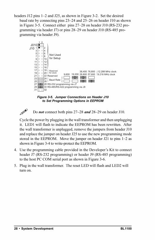
J10J010
1 2
13579
1113151719212325272931
2468101214161820222426283032
Baud Rate
Not Usedfor Setup
Reserved9,600 19,200
38,40028,800
76,80057,600
12.288 MHz clock9.216 MHz clock
RS-232 programming via J7RS-485/RS-422 programming via J9
Reservedfor clock
!
headers J12 pins 12 and J25, as shown in Figure 3-2. Set the desiredbaud rate by connecting pins 2324 and 2526 on header J10 as shownin Figure 3-5. Connect either pins 2728 on header J10 (RS-232 pro-gramming via header J7) or pins 2829 on header J10 (RS-485 pro-gramming via header J9).
Figure 3-5. Jumper Connections on Header J10to Set Programming Options in EEPROM
Do not connect both pins 2728 and 2829 on header J10.
Cycle the power by plugging in the wall transformer and then unpluggingit. LED1 will flash to indicate the EEPROM has been rewritten. Afterthe wall transformer is unplugged, remove the jumpers from header J10and replace the jumper on header J25 to use the new programming modestored in the EEPROM. Move the jumper on header J21 to pins 12 asshown in Figure 3-4 to write-protect the EEPROM.
4. Use the programming cable provided in the Developers Kit to connectheader J7 (RS-232 programming) or header J9 (RS-485 programming)to the host PC COM serial port as shown in Figure 3-6.
5. Plug in the wall transformer. The reset LED will flash and LED2 willturn on.

BL1100 System Development s 29
J12
J11
J10
J6
J7
J8
J9
J1
J2
J3
J13
J23
RP6J18
J31
J30
To PC
DB-9 connector
RS-485/RS-422to RS-232converter
J9 (RS-485programming)
J12
J11
J10
J6
J7
J8
J9
J1
J2
J3
J13
J23
RP6J18
J31
J30
To PC
DB-9 connector
9-pin to 25-pinadapter
(optional)
Serial cableto PC
J7
1
Serial cableto PC
J9
1
(a) RS-232
J7 (RS-232programming)
(b) RS-485
Figure 3-6. Programming Cable Connections
A commercially available RS-485/RS-422 to RS-232 converteris required as shown in Figure 3-6 if your PC COM serial portis RS-232 and you wish to program in the RS-485 mode.
!
BL110030 s System Development
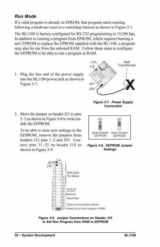
Run ModeIf a valid program is already in EPROM, that program starts runningfollowing a hardware reset or a watchdog timeout as shown in Figure 3-1.
The BL1100 is factory-configured for RS-232 programming at 19,200 bps.In addition to running a program from EPROM, which requires burning anew EPROM to replace the EPROM supplied with the BL1100, a programmay also be run from the onboard RAM. Follow these steps to configurethe EEPROM to be able to run a program in RAM.
Figure 3-7. Power SupplyConnection
Heat
J12
J11
J10
J6
J7
J8
J9
J1
J2
J3
J13
J23
RP6J18
J31
J30
J25
WallTransformer
X
J12
J21
J21
J10
1. Plug the free end of the power supplyinto the BL1100 power jack as shown inFigure 3-7.
Write-EnableEEPROM
J21
Write-ProtectEEPROM
J21
Figure 3-8. EEPROM JumperSettings
2. Move the jumper on header J21 to pins23 as shown in Figure 3-8 to write-en-able the EEPROM.
To be able to store new settings in theEEPROM, remove the jumpers fromheaders J12 pins 12 and J25. Con-nect pins 3132 on header J10 asshown in Figure 3-9.
Figure 3-9. Jumper Connections on Header J10to Set Run Program from RAM in EEPROM
J10J010
1 2
13579
1113151719212325272931
2468101214161820222426283032
Baud Rate
Not Usedfor Setup
Reserved
Connect to run user program in RAM
Serial communication options
Reservedfor clock

BL1100 System Development s 31
3. Cycle the power by plugging in the wall transformer and then unpluggingit. LED1 will flash to indicate the EEPROM has been rewritten. Afterthe wall transformer is unplugged, remove the jumper from header J10and replace the jumper on header J25 to use the new configuration storedin the EEPROM. Move the jumper on header J21 to pins 12 as shown inFigure 3-8 to write-protect the EEPROM.
4. Plug in the wall transformer. The reset LED will flash and the programin RAM will execute.
Switching Between Run and Program ModeTo return to Program Mode, follow the instructions in the ProgrammingOptions section in this chapter. The Run Mode steps will have to beperformed if the EEPROM is rewrittten for programming.
To switch to factory-default RS-232 programming at 19,200 bpswithout rewriting the EEPROM, it is possible to toggle be-tween run and program mode by placing a jumper across pins12 of header J12 (program mode) or by removing the jumperacross pins 12 of header J12 (run mode).
RS-485 programming at 57,600 bps is also possible withoutrewriting the EEPROM by removing the jumper on header J25and placing a jumper across pins 12 of header J12 (programmode). To return to run mode, replace the jumper on headerJ25 and remove the jumper across pins 12 of header J12.
Tip
Tip

BL110032 s System Development
Memory
EPROMThe development EPROM supplied with the BL1100 in socket U011 mustbe used when programming the BL1100 with Dynamic C. The develop-ment EPROM has the following format for its part number.
680-20nn where nn indicates the revision number for the BIOS
The 32-pin socket (U011) for the development EPROM accepts 32K to 512K
EPROM chips. The socket accepts either 28-pin or 32-pin EPROM chips,including the following.
27C256 32K 28 pins27C512 64K 28 pins27C010 128K 32 pins27C020 256K 32 pins
When using a 28-pin EPROM, four pin positions at one end of the socketare left empty, as shown in Figure 3-10. The access time must be 100 ns orbetter at 9 MHz.
Header J16 reflects whether the amount of memory, and header J20 reflectsthe number of pins, as shown in Figure 3-10.
Figure 3-10. 28-pin and 32-pin EPROM Placementand Jumper Configurations
32-pinEPROM28-pin
EPROM
U011
U011
J203
2
1
J203
2
1
J16
1 2 3
J16
1 2 3
J16
1 2 3
J16
32K or smaller EPROM64K or larger EPROM
BL1100 System Development s 33
Programming EPROMDynamic C can be used to create a file for programming an EPROM byselecting the Compile to File option in the COMPILE menu with thedevelopment EPROM installed. The BL1500 must be connected to the PCrunning Dynamic C during this step because essential library routines mustbe uploaded from the development EPROM and linked to the resultingfile. The output is a binary file (optionally an Intel hex format file) thatcan be used to build an application EPROM. The application EPROM isthen programmed with an EPROM programmer that reads either a binaryimage or the Intel hex format file. The resulting application EPROM canthen replace the development EPROM.
CopyrightsThe Dynamic C library is copyrighted. Place a label containing thefollowing copyright notice on the EPROM whenever an EPROM thatcontains portions of the Dynamic C library is created.
©1995 Z-World
Your own copyright notice may also be included on the label to protectyour portion of the code.
Z-World grants purchasers of the Dynamic C software and the copyrightedBL1100 EPROM permission to copy portions of the EPROM library asdescribed above, provided that:
1. The resulting EPROM is used only with the BL1100 manufac-tured by Z-World, and
2. Z-Worlds copyright notice is placed on all copies of the EPROM.
SRAMWhen doing program development with Dynamic C, it is best to use a128K SRAM, supplied with the Developers Kit, or larger. Dynamic Cwill work with a 32K SRAM, but the total program space will be limited to16K of root and 16K of extended memory. This is enough for manyprograms, but it is inconvenient to run out of memory during development.Once a program is burned into EPROM, there is no reason to use SRAMlarger than 32K unless the data space is larger than 32K.
The BL1100 SRAM is socketed, and is found at U10 just to the right of theEPROM.

BL110034 s System Development
BL1100 Subsystems 35
CHAPTER 4: SUBSYSTEMS
Chapter 4 describes the BL1100 hardware subsystems and digitalinerfaces. The following sections are included.• Interface Overview• Power-Supervisor Integrated Circuit• Digital Interfaces• Serial Communication• Direct Programming using Serial Ports• Asynchronous Serial Communication Interface• SIO Serial Ports
BL110036 s Subsystems
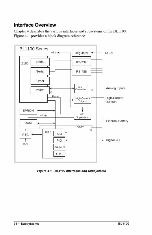
Interface OverviewChapter 4 describes the various interfaces and subsystems of the BL1100.Figure 4-1 provides a block diagram reference.
Figure 4-1. BL1100 Interfaces and Subsystems
Z180
Regulator DCIN+5 V
Timer
RS-485
RTC
RAM
KIOSIO
Reset
Digital I/O
BL1100 Series
External Battery
PIO
CTC
A/DConverter
VBAT
VRAM
+5 V
EPROM
PIA/MUX
691Supervisor
RS-232
Analog Inputs
Serial
Serial
CSI/O
High-CurrentDrivers
High-CurrentOutputs
BL1100 Subsystems s 37
Power-Supervisor Integrated CircuitThe 691 power-supervisor IC is a key component that helps a system tosurvive power fluctuations and power outages. Several vital servicesprovided by the power supervisor are described below.
Power-on reset
The supervisor IC generates the power-on reset for the BL1100 by holding/RESET low until the IC senses that VCC has risen above the reset thresh-old (~4.65 V) and the battery voltage (2.5 V to 4.25 V DC). When VCCfalls below the threshold, the supervisor IC disables the RAM to preventspurious writing of data.
RAM protection
The power-supervisor IC gates the RAMs write-enable line (BATACT)whenever VCC is above the reset threshold and VBAT. When VCC fallsbelow the threshold, the 691 de-asserts BATACT to prevent spuriouswriting to the RAM.
Watchdog timer
The watchdog timer is enabled by placing a jumper across header 22. Thewatchdog timer guards against system or software faults. If an applicationdoes not hit the watchdog timer at least every 1.0 seconds, the watchdogtimer resets the Z180. The supervisors watchdog output (/WDO) con-nects to the Z180s /INT1 inetrrupt line. /WDO is at logic zero level aftera watchdog reset and at logic 1 after a power-on reset.
To hit the watchdog timer, make a call to the library functionhitwd. This call makes a dummy one-byte DMA transfer viaDMA channel 1, which activates the DMA-end signal, /TEND1,hitting the watchdog timer.
Nonmaskable interrupt
The 691 generates a nonmaskable interrupt (/HNMI) from its power-failoutput (/PFO) for the microprocessor if the unregulated DC input (nor-mally 9 V DC) falls below 7.6 V. This gives the BL1100 advancedwarning of an impending power failuire, which allows it to executeshutdown routines. The voltage divider (R25 and R27) determines thepower-fail voltage level.
/HNMI also connects to the KIO to allow your software to monitor the/HNMI line after the nonmaskable interrupt, and to recover from tempo-rary low-input-voltage conditions or brownouts.
Backup-battery switchover
The 691 switches the RAM over to battery power if VCC falls below thebattery voltage, VBAT (2.5 V to 4.25 V DC).
!

BL110038 s Subsystems
Digital InterfacesThe BL1100 has several digital interfaces.
KIO interface
16-bit PIO (parallel I/O and keypad interface)
Counter/timers circuit (CTC)
High-current/high-voltage driver
Liquid crystal display (LCD)
Zilog KIO InterfaceThe Zilog KIO interface chip (U9) is an 84-pin LSI chip that combinesseveral functions into one package. Figure 4-2 is a block diagram of thefunctions performed by the KIO interface chip.
Figure 4-2. KIO Block Diagram
The KIO integrates the following three peripheral functions.
PIO 16-line parallel I/O
SIO dual-channel serial I/O controller
CTC quad counter/timer
CTCQuad Counter/Timer
SIODual ChannelSerial InputOutputController
PIA / MUX
PIO16 line parallelinterface
Oscillator
Bus
Interface
and
Control
InterruptControl

BL1100 Subsystems s 39
KIO Command RegisterThe KIO command register provides overall control of its functions.Figure 4-3 illustrates the layout of the command register.
Figure 4-3. KIO Command Register Layout
The reset bits cause a momentary reset when a 1 is stored. The daisychain establishes the relative interrupt priority of the various functionsthat make up the KIO. To modify the daisy chain, store a 1 in bit 3 at thesame time as the new daisy chain configuration. Choice 011 in Figure 4-3is the default set by Dynamic C. The following function sets the daisychain where code is delineated in Figure 4-3.
int setdaisy( byte code );
The default setting gives the CTC the highest priority.
Bit 7 in the KIO command register is normally turned on by Dynamic C sothat the SIO can be used.
The relative position on the daisy chain determines which interrupt willoccur first when several are pending. All interrupts from the KIO arehigher in priority than interrupts from the Z180s internal devices, exceptNMI and illegal instruction trap interrupts.
Reset PIO
Daisy chain write enable
Reset CTC
Reset SIO
SIO/ PIA Mux 0 = PIO 1 = SIO
000 None 001 SIO, CTC, PIO 010 SIO, PIO, CTC 011 CTC, SIO, PIO 100 CTC, PIO, SIO 101 PIO, SIO, CTC 110 PIO, CTC, SIO 111 None
Daisy Chain ConfigurationKIO Command Register address = 4E
D0D7 D6 D5 D4 D3 D2 D1

BL110040 s Subsystems
PIO InterfaceThe PIO unit in the KIO provides a 16-bit parallel interface. Figure 4-4 isa block diagram of the PIO parallel interface.
Figure 4-4. PIO Chip and Keypad Interface
Lines PA0PA7 are considered as Port A and lines PB0PB7 areconsidered as Port B. Each line can serve as an input or output indifferent modes. The four lines on J12 are handshaking lines that consistof a ready line and a strobe line for each port.
J11 is designed to hold a special user-installed connector that clamps on to theflexible circuit ribbon of a membranekeypad. A membrane keypad is a matrixarray like the one shown Figure 4-5.
The PIO can read this keypad by settingeach row to zero volts and monitoringeach column. Columns are held up bypull-up resistors. The microprocessor canuse the PIO to detect closure of any key in the keypad. Debouncing must bedone by software.
The impedance of the PIO is approximately 80 W for sinking current and160 W for sourcing current. Do not apply voltages below ground or aboveVCC to the PIO.
1
2
PA0
PA1
PA2
PA3
PA4
PA5
PA6
PA7
PB0
PB1
PB2
PB3
PB4
PB5
PB6
PB7
3
4
5
8
9
10
11
12
13
14
15
16
7
6
J010
J10
1
3
5
7
9
1517
19
21
23
25
27
29
31
13
11
4 /STBB
J12
/STBA 3
RDYA 5
RDYB 7
J10 and J010together constitutea single 34-pinconnector.
not socketedJ11
+5 V10 kΩ
10 kΩ
+5 V +5 V
Figure 4-5.Keypad Matrix Array
BL1100 Subsystems s 41
The PIO is very flexible and has a number of modes of operation. The twoports are controlled by the following four registers.
40H (PIODA) PIO Port A, data41H (PIOCA) PIO Port A, command42H (PIODB) PIO Port B, data43H (PIOCB) PIO Port B, command
Each register pair controls one of the 8-bit ports and the two handshakinglines associated with each port. The ports four modes of operation are asfollows.
Mode 0strobed byte outputMode 1strobed byte inputMode 2bidirectional data transfer (port A only)Mode 3bitwise I/O, input/output selectable per bit
Mode 0 (Strobed Byte Output)
When the microprocessor stores a byte in a ports data register, the eightassociated output lines change level according to how each bit is set: levelhigh for a 1 or level low for a 0. The ready handshake line goes high. Theready line is reset when an external device pulses the strobe line (low) . Ifinterrupts are enabled for the port, a PIO interrupt is requested. Thisallows for interrupt-driven parallel output.
Mode 1 (Strobed Byte Input)
The PIO latches eight bits into a register when it receives the strobe signalfrom an external device. The strobe signal also causes the ready line to golow. An interrupt is then requested. After the microprocessor reads the regis-ter, the ready line is raised to indicate that the port is ready for another byte.
Mode 2 (Bidirectional Data Transfer)
This mode uses Port A and all four handshake lines. Data can be trans-ferred in both directions under control of the four handshake lines.
Mode 3 (Bitwise I/O)
Mode 3 is a general-purpose input-output mode. Each bit can be specifiedindividually as input or output. In this mode, the input lines can also serveas interrupt request lines. Either transition to high or transition to low canbe specified for the interrupt request. Interrupts for specific input lines arecontrolled with a mask and by specifying an AND or an OR function forthe masked lines. Interrupts on PIO ports are edge-triggered.

BL110042 s Subsystems
Using PIO PortsTo set up a port for I/O, first write a sequence of bytes to its commandregister. Then read, or write, its data register to transfer data. The sampleprogram PIODEMO.C illustrates the use of the PIO registers.
The control register byte sequence is shown below.
Mode control wordI/O register control word (only if Mode 3)Interrupt vector wordInterrupt control wordMask control wordInterrupt disable word
The mode control word specifies the mode for the port as shown inFigure 4-6.
Figure 4-6. PIO Mode Control Word
The I/O register control word must immediately follow the mode controlword, but only when the mode is 3 (bitwise I/O). This specifies which bitsare inputs and which bits are outputs for bitwise I/O.
Figure 4-7. PIO Register Control Word
0 0 = mode 00 1 = mode 11 0 = mode 21 1 = mode 3
Identifies this asmode control word
1D7 D6 X X 1 1 1
0 bit is output1 bit is input
D0D7 D6 D5 D4 D3 D2 D1
BL1100 Subsystems s 43
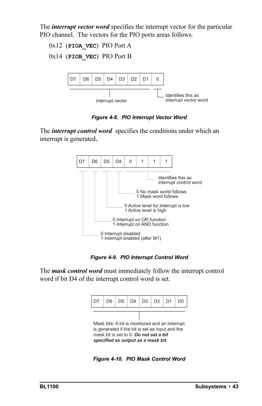
The interrupt vector word specifies the interrupt vector for the particularPIO channel. The vectors for the PIO ports areas follows.
0x12 (PIOA_VEC) PIO Port A
0x14 (PIOB_VEC) PIO Port B
Figure 4-8. PIO Interrupt Vector Word
The interrupt control word specifies the conditions under which aninterrupt is generated.
Figure 4-9. PIO Interrupt Control Word
The mask control word must immediately follow the interrupt controlword if bit D4 of the interrupt control word is set.
Figure 4-10. PIO Mask Control Word
interrupt vectorIdentifies this asinterrupt vector word
0D7 D6 D5 D4 D3 D2 D1
0 No mask world follows1 Mask word follows
Identifies this asinterrupt control word
1D7 D6 D5 D4 0 1 1
0 Active level for interrupt is low1 Active level is high
0 Interrupt on OR function1 Interrupt on AND function
0 Interrupt disabled1 Interrupt enabled (after M1)
Mask bits: A bit is monitored and an interruptis generated if the bit is set as input and themask bit is set to 0. Do not set a bitspecified as output as a mask bit.
D0D7 D6 D5 D4 D3 D2 D1
BL110044 s Subsystems
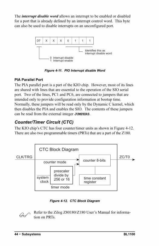
The interrupt disable word allows an interrupt to be enabled or disabledfor a port that is already defined by an interrupt control word. This bytecan also be used to disable interrupts on an unconfigured port.
Figure 4-11. PIO Interrupt disable Word
PIA Parallel Port
The PIA parallel port is a part of the KIO chip. However, most of its linesare shared with lines that are essential to the operation of the SIO serialport. Two of the lines, PC1 and PC6, are connected to jumpers that areintended only to provide configuration information at bootup time.Normally, these jumpers will be read only by the Dynamic C kernel, whichthen disables the PIA and enables the SIO. The contents of these jumperscan be read from the external integer JUMPERS.
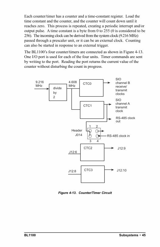
Counter/Timer Circuit (CTC)The KIO chips CTC has four counter/timer units as shown in Figure 4-12.There are also two programmable timers (PRTs) that are a part of the Z180.
Figure 4-12. CTC Block Diagram
Refer to the Zilog Z80180/Z180 Users Manual for informa-tion on PRTs.
Identifies this asinterrupt disable word
1D7 X X X 0 1 1
0 Interrupt disable1 Interrupt enable
counter modeCLK/TRG
timer mode
systemclock
prescalerdivide by256 or 16
counter 8-bits
time constantregister
ZC/T0
CTC Block Diagram
$
BL1100 Subsystems s 45
Each counter/timer has a counter and a time-constant register. Load thetime constant and the counter, and the counter will count down until itreaches zero. This process is repeated, creating a periodic interrupt and/oroutput pulse. A time constant is a byte from 0 to 255 (0 is considered to be256). The incoming clock can be derived from the system clock (9.216 MHz)passed through a prescaler unit, or it can be an external clock. Countingcan also be started in response to an external trigger.
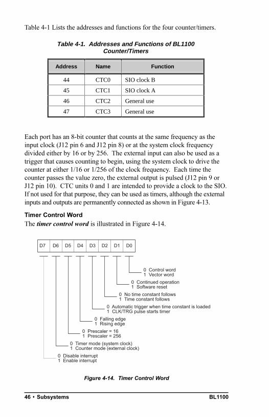
The BL1100s four counter/timers are connected as shown in Figure 4-13.One I/O port is used for each of the four units. Timer commands are sentby writing to the port. Reading the port returns the current value of thecounter without disturbing the count in progress.
Figure 4-13. Counter/Timer Circuit
CTC0divideby2
9.216MHz
4.608MHz
HeaderJ014
SIOchannel Breceive/transmitclocks
CTC1
SIOchannel Atransmitclock
1 2
3 4
CTC2J12:6
J12:9
CTC3J12:8 J12:10
RS-485 clockout
RS-485 clock in
BL110046 s Subsystems
Table 4-1 Lists the addresses and functions for the four counter/timers.
Each port has an 8-bit counter that counts at the same frequency as theinput clock (J12 pin 6 and J12 pin 8) or at the system clock frequencydivided either by 16 or by 256. The external input can also be used as atrigger that causes counting to begin, using the system clock to drive thecounter at either 1/16 or 1/256 of the clock frequency. Each time thecounter passes the value zero, the external output is pulsed (J12 pin 9 orJ12 pin 10). CTC units 0 and 1 are intended to provide a clock to the SIO.If not used for that purpose, they can be used as timers, although the externalinputs and outputs are permanently connected as shown in Figure 4-13.
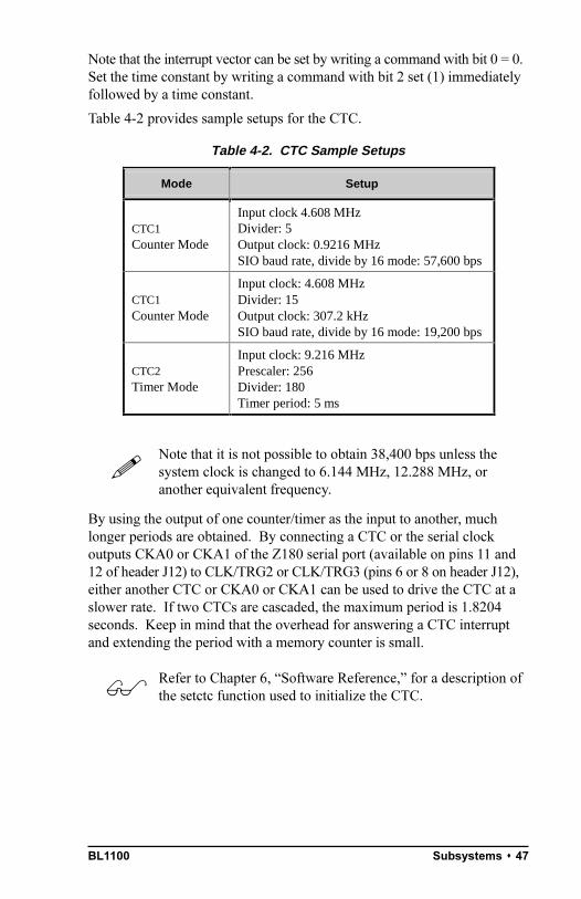
Timer Control Word
The timer control word is illustrated in Figure 4-14.
Figure 4-14. Timer Control Word
Table 4-1. Addresses and Functions of BL1100Counter/Timers
Address Name Function
44 CTC0 SIO clock B
45 CTC1 SIO clock A
46 CTC2 General use
47 CTC3 General use
0 Control word1 Vector word
D0D7 D6 D5 D4 D3 D2 D1
0 Continued operation1 Software reset
0 No time constant follows1 Time constant follows
0 Automatic trigger when time constant is loaded1 CLK/TRG pulse starts timer
0 Falling edge1 Rising edge
0 Prescaler = 161 Prescaler = 256
0 Timer mode (system clock)1 Counter mode (external clock)
0 Disable interrupt1 Enable interrupt
BL1100 Subsystems s 47
Note that the interrupt vector can be set by writing a command with bit 0 = 0.Set the time constant by writing a command with bit 2 set (1) immediatelyfollowed by a time constant.
Table 4-2 provides sample setups for the CTC.
Note that it is not possible to obtain 38,400 bps unless thesystem clock is changed to 6.144 MHz, 12.288 MHz, oranother equivalent frequency.
By using the output of one counter/timer as the input to another, muchlonger periods are obtained. By connecting a CTC or the serial clockoutputs CKA0 or CKA1 of the Z180 serial port (available on pins 11 and12 of header J12) to CLK/TRG2 or CLK/TRG3 (pins 6 or 8 on header J12),either another CTC or CKA0 or CKA1 can be used to drive the CTC at aslower rate. If two CTCs are cascaded, the maximum period is 1.8204seconds. Keep in mind that the overhead for answering a CTC interruptand extending the period with a memory counter is small.
Refer to Chapter 6, Software Reference, for a description ofthe setctc function used to initialize the CTC.
Table 4-2. CTC Sample Setups
Mode Setup
CTC1Counter Mode
Input clock 4.608 MHzDivider: 5Output clock: 0.9216 MHzSIO baud rate, divide by 16 mode: 57,600 bps
CTC1Counter Mode
Input clock: 4.608 MHzDivider: 15Output clock: 307.2 kHzSIO baud rate, divide by 16 mode: 19,200 bps
CTC2Timer Mode
Input clock: 9.216 MHzPrescaler: 256Divider: 180Timer period: 5 ms
!
$
BL110048 s Subsystems
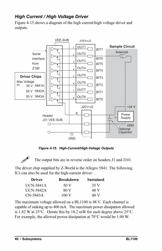
High Current / High Voltage DriverFigure 4-15 shows a diagram of the high current/high voltage driver andoutputs.
Figure 4-15. High-Current/High-Voltage Outputs
The output bits are in reverse order on headers J1 and J101.
The driver chip supplied by Z-World is the Allegro 5841. The followingICs can also be used for the high-current driver:
Driver Breakdown SustainedUCN-5841A 50 V 35 VUCN-5842A 80 V 48 VCN-5843A 100 V 48 V
The maximum voltage allowed on a BL1100 is 48 V. Each channel iscapable of sinking up to 400 mA. The maximum power dissipation allowedis 1.82 W at 25°C. Derate this by 18.2 mW for each degree above 25°C.For example, the allowed power dissipation at 70°C would be 1.00 W.
BIT6
OUT1
OUT2
OUT3
OUT4
OUT5
OUT6
OUT7
OUT8
PowerSupply
GND
J201=J2
K
GND
HeaderJ31 VEE-SUB
BIT7
BIT5
BIT4
BIT3
BIT2
BIT1
BIT0
Solenoid
J101=J1VEE-SUB
Serial
Interface
from
Z180
OptionalCapacitor
+24 V
1
2
3
4
5
6
7
8
Driver Chips
Sample Circuit
5841A
5842A
5843A
35 V
50 V
50 V
Max Voltagein:
!

BL1100 Subsystems s 49
The collector to emitter saturation voltage must not exceed the followingvalues:
Current C-E Voltage Power Dissipation100 mA 1.1 V 0.11 W200 mA 1.3 V 0.26 W350 mA 1.6 V 0.56 W
The VEE pin can be up to 20 V negative with respect to ground, as whenusing split power supplies, but it is important that the ground be locatedbetween the plus and minus power supply voltage (no floating supply isallowed). This driver is designed to drive inductive loads such as sole-noids or relays.
The K line drains inductive voltage excesses. If the wireconnecting K to the power supply is long (inductive), place alocal filter capacitor near the board to absorb the voltage surgewhen the device is turned off.
When driving incandescent lights, beware of the initial inrush currentstressing the driver. It is not advisable to use the unregulated directcurrent into the board if there is any danger that the load will cause thepower-fail circuitry of the BL1100 to be triggered. If unregulated input tothe board is not used, be sure to take the current directly from the supplyand not from the board connector. It is easy to blow out the driver chip byconnecting and removing wires with the power enabled. If the protectivediodes are not connected, inductive loads will ruin the chip immediately.
The high-voltage driver is not affected when a hardware reset occurs. Takespecial precautions if it is important to disable the high-voltage driver onsystem failure. For example, build an independent turn-off mechanism forequipment controlled by the high-voltage driver chip.
If the BL1100 power supply fails, then the high-voltage driverwill be placed in the OFF state and remain off when powerreturns. If the 5841 chip fails due to stress, it can fail in theON state, allowing current to flow. Be sure to consider theconsequences of any such failure, and take appropriateprotective precautions when necessary.
!
BL110050 s Subsystems
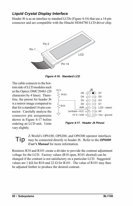
Liquid Crystal Display InterfaceHeader J6 is as an interface to standard LCDs (Figure 4-16) that use a 14-pinconnector and are compatible with the Hitachi HD44780 LCD driver chip.
Figure 4-16. Standard LCD
The cable connects to the bot-tom side of LCD modules suchas the Optrex DMC20481 (20characters by 4 lines). There-fore, the pinout for header J6is a mirror image compared tothat for a standard 14-pin con-nector. Carefully analyze theconnector pin assignmentsshown in Figure 4-17 beforeordering an LCD unit. Unitsvary slightly.
Z-Worlds OP6100, OP6200, and OP6300 operator interfacesmay be connected directly to header J6. Refer to the OP6000Users Manual for more information.
Resistors R10 and R101 create a divider to provide the contrast adjustmentvoltage for the LCD. Factory values (R10 open, R101 shorted) can bechanged if the contrast is not satisfactory on a particular LCD. Suggestedvalues are 1 kW for R10 and 22 W for R101. The value of R101 may thenbe adjusted further to produce the desired contrast.
Pin 1
Pin 2
Pin 14
LCD
contrastVLC+5 VVdd
R101
R10
12
1314
D7D5D3D1LCD - selectA0Vss - ground
D6D4D2D0
4 3
6 5
8 7
9
10 10
10/WR
J6+5 V
Figure 4-17. Header J6 Pinout
Tip
BL1100 Subsystems s 51
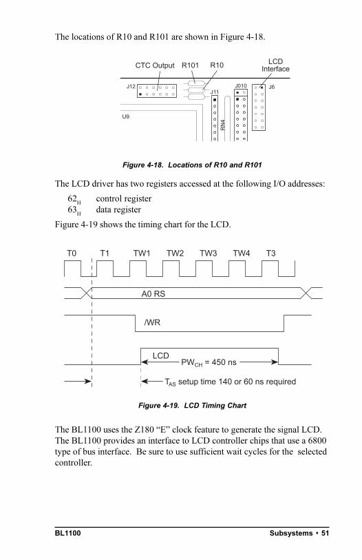
The locations of R10 and R101 are shown in Figure 4-18.
Figure 4-18. Locations of R10 and R101
The LCD driver has two registers accessed at the following I/O addresses:
62H
control register63
Hdata register
Figure 4-19 shows the timing chart for the LCD.
Figure 4-19. LCD Timing Chart
The BL1100 uses the Z180 E clock feature to generate the signal LCD.The BL1100 provides an interface to LCD controller chips that use a 6800type of bus interface. Be sure to use sufficient wait cycles for the selectedcontroller.
CTC Output LCDInterface
KIO
J12 J6
U9
RN
4
J11
R101 R10
J010
T0 T1 TW1 TW2 TW4TW3 T3
A0 RS
TAS setup time 140 or 60 ns required
PWCH = 450 ns
/WR
LCD
BL110052 s Subsystems
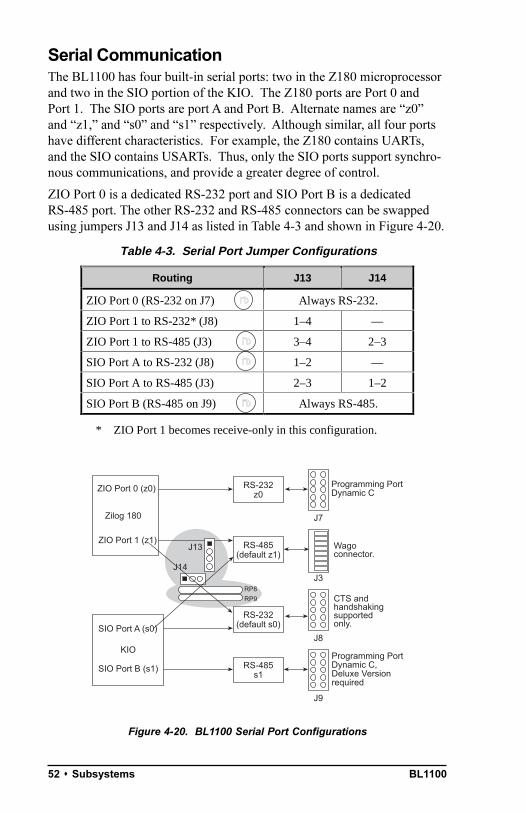
Serial CommunicationThe BL1100 has four built-in serial ports: two in the Z180 microprocessorand two in the SIO portion of the KIO. The Z180 ports are Port 0 andPort 1. The SIO ports are port A and Port B. Alternate names are z0and z1, and s0 and s1 respectively. Although similar, all four portshave different characteristics. For example, the Z180 contains UARTs,and the SIO contains USARTs. Thus, only the SIO ports support synchro-nous communications, and provide a greater degree of control.
ZIO Port 0 is a dedicated RS-232 port and SIO Port B is a dedicatedRS-485 port. The other RS-232 and RS-485 connectors can be swappedusing jumpers J13 and J14 as listed in Table 4-3 and shown in Figure 4-20.
Figure 4-20. BL1100 Serial Port Configurations
Table 4-3. Serial Port Jumper Configurations
Routing J13 J14
ZIO Port 0 (RS-232 on J7) Always RS-232.
ZIO Port 1 to RS-232* (J8) 1–4 —
ZIO Port 1 to RS-485 (J3) 3–4 2–3
SIO Port A to RS-232 (J8) 1–2 —
SIO Port A to RS-485 (J3) 2–3 1–2
SIO Port B (RS-485 on J9) Always RS-485.
* ZIO Port 1 becomes receive-only in this configuration.
FD
FD
FD
FD
SIO Port A (s0)
SIO Port B (s1)
ZIO Port 0 (z0)
ZIO Port 1 (z1)
Zilog 180
KIO
J13
J14
RS-485(default z1)
RS-232(default s0)
RS-232z0
RS-485s1
J7
J8
CTS andhandshakingsupportedonly.
J9
J3
Wagoconnector.
Programming PortDynamic C
Programming PortDynamic C,Deluxe Versionrequired
RP8RP9
BL1100 Subsystems s 53
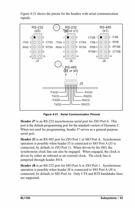
Figure 4-21 shows the pinout for the headers with serial communicationsignals.
Figure 4-21. Serial Communication Pinouts
Header J7 is an RS-232 asynchronous serial port for ZIO Port 0. Thisport is the default programming port for the standard version of Dynamic C.When not used for programming, header J7 serves as a general-purposeserial port.
Header J3 is an RS-485 port for ZIO Port 1 or SIO Port A. Synchronousoperation is possible when header J3 is connected to SIO Port A (J3 isconnected, by default, to ZIO Port 1). When driven by the SIO, thesynchronous clock line can also be engaged. When engaged, the clock isdriven by either an onboard or an external clock. The clock line isjumpered through header J014.
Header J8 is an RS-232 port for SIO Port A or ZIO Port 1. Synchronousoperation is possible when header J8 is connected to SIO Port A (J8 isconnected, by default, to SIO Port A). Only CTS and RTS handshake linesare supported.
J7
/RX0
/TX0 CTS0
1
3
5
7
9
2
4
6
8
10
RTS0
RS-232(z0)
J8
/RXA
/TXA CTSA
1
3
5
7
9
2
4
6
8
10
RTSA
RS-232(s0 or z1)
J9
TXB
CTSB /TXB1
3
5
7
9
2
4
6
8
10
/RXB
RS-485(s1)
/RTSB
/CTSBRTSB
RXB
18
J3
/RXDD
/RXCD
RXCD
RXDD
TXDD
/TXDD
/TXCD
RS-485(z1 or s0)
FD
FD
TXCD

BL110054 s Subsystems
Header J9 is an RS-485 asynchronous or synchronous port for SIO Port B.This port is the high speed programming port for the deluxe version ofDynamic C. The handshaking lines are not used by Dynamic C, but can beused if the port is diverted to another purpose.
RS-232 Communication
Modem CommunicationModems and telephone lines allow RS-232 communication across great dis-tances. A modem automatically scans character streams that are read fromthe receive buffer for modem com-mands. The RS-232 library supportscommunication with a Hayes SmartModem or another compatible mo-dem. If the modem is not compat-ible, you must tie the CTS, RTS, andDTR lines on the modem side to-gether. Additionally, the CTS andRTS lines on the BL1100 side alsohave to be tied together. A NULLconnection is also required for theTX and the RX lines. However, acommercial NULL modem alreadyhas its CTS and RTS lines tied to-gether on both sides.
Figure 4-22 illustrates the connections between a BL1100 and a modem.
See Z-Worlds Dynamic C reference manuals for details on thesoftware functions used for modem communication.
XMODEM File TransferThe BL1100 supports the XMODEM protocol for downloading anduploading data. Currently, the library supports downloading an array ofdata in multiples of 128 bytes.
Uploaded data are written to a specified area in RAM. The targetedwriting area should not conflict with the current resident program or data.
Character echo is automatically suspended during XMODEM transfer.
RXTX
GNDRTSCTSDTR
RXTXGNDRTSCTS
ModemSide
BL1100Side
Figure 4-22. Connections BetweenController and Modem
$
BL1100 Subsystems s 55
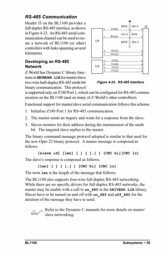
RS-485 CommunicationHeader J3 on the BL1100 provides afull-duplex RS-485 interface, as shownin Figure 4-23. An RS-485 serial com-munication channel can be used to cre-ate a network of BL1100 (or other)controllers with links spanning severalkilometers.
Developing an RS-485NetworkZ-World has Dynamic C library func-tions in NETWORK.LIB for master/slavetwo-wire half-duplex RS-485 ninth-bitbinary communication. This protocolis supported only on Z180 Port 1, which can be configured for RS-485 commu-nication on the BL1100 (and on many of Z-Worlds other controllers).
Functional support for master/slave serial communication follows this scheme.
1. Initialize Z180 Port 1 for RS-485 communication.
2. The master sends an inquiry and waits for a response from the slave.
3. Slaves monitor for their address during the transmission of the ninthbit. The targeted slave replies to the master.
The binary command message protocol adopted is similar to that used forthe new Opto 22 binary protocol. A master message is composed asfollows.
[slave id] [len] [ ] [ ][ ] [CRC hi][CRC lo]
The slaves response is composed as follows.
[len] [ ] [ ][ ] [CRC hi] [CRC lo]
The term len is the length of the message that follows.
The BL1100 also supports four-wire full-duplex RS-485 networking.While there are no specific drivers for full-duplex RS-485 networks, themaster may be enable with a call to on_485 in the DRIVERS.LIB library.Slaves have to be turned on and off with on_485 and off_485 for theduration of the message they have to send.
Refer to the Dynamic C manuals for more details on master/slave networking.
1
2
J32
1
RP9
680 Ω
680 Ω
220 Ω
RXDD
/RXDD
RP9
RP8
6
7
RXCD/RXCD
3
4
U4
U3
2
3
TXDD/TXDD
5
66
5
TXCD/TXCD
7
8
Figure 4-23. RS-485 Interface
$
BL110056 s Subsystems
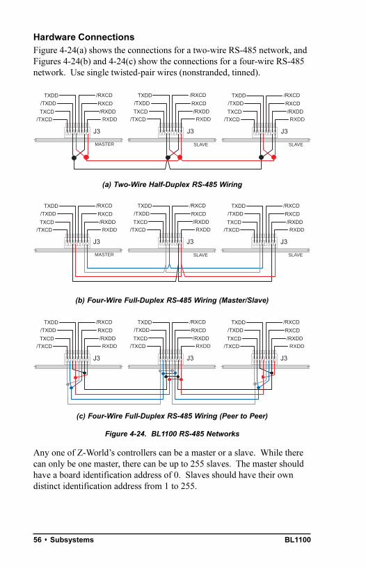
Hardware ConnectionsFigure 4-24(a) shows the connections for a two-wire RS-485 network, andFigures 4-24(b) and 4-24(c) show the connections for a four-wire RS-485network. Use single twisted-pair wires (nonstranded, tinned).
(a) Two-Wire Half-Duplex RS-485 Wiring
(b) Four-Wire Full-Duplex RS-485 Wiring (Master/Slave)
(c) Four-Wire Full-Duplex RS-485 Wiring (Peer to Peer)
Figure 4-24. BL1100 RS-485 Networks
Any one of Z-Worlds controllers can be a master or a slave. While therecan only be one master, there can be up to 255 slaves. The master shouldhave a board identification address of 0. Slaves should have their owndistinct identification address from 1 to 255.
J3
/RXCD
RXCD
RXDD
TXDD
/TXDD
/TXCDTXCD /RXDD
J3
/RXCD
RXCD
RXDD
TXDD
/TXDD
/TXCDTXCD /RXDD
J3
/RXCD
RXCD
RXDD
TXDD
/TXDD
/TXCDTXCD /RXDD
SLAVE SLAVEMASTER
J3
/RXCD
RXCD
RXDD
TXDD
/TXDD
/TXCDTXCD /RXDD
J3
/RXCD
RXCD
RXDD
TXDD
/TXDD
/TXCDTXCD /RXDD
J3
/RXCD
RXCD
RXDD
TXDD
/TXDD
/TXCDTXCD /RXDD
MASTER SLAVE SLAVE
J3
/RXCD
RXCD
RXDD
TXDD
/TXDD
/TXCDTXCD /RXDD
J3
/RXCD
RXCD
RXDD
TXDD
/TXDD
/TXCDTXCD /RXDD
J3
/RXCD
RXCD
RXDD
TXDD
/TXDD
/TXCDTXCD /RXDD
BL1100 Subsystems s 57
Termination and bias resistors are required in a multidrop network tominimize reflections (echoing), and to keep the network line active in anidle state. The BL1100 has 220 W termination resistors (RP8) and 680 W(RP9) bias resistors already installed. Remove the RP9 resistor packsfrom all the slave controllers, and remove the RP8 resistor packs from allthe slave controllers except the last one.
Z-World recommends placing a 220 W termination resistoracross the twisted-wire pair for the last slave unit instead ofusing RP8. This will ensure that a termination resistor remainsin place if the slave is substituted.
Connect the grounds (pin 8 of Wago connector J2) of your RS-485 network to eliminate network faults resulting from thegrounds being at different potentials.
Refer to National Semiconductor Application Note 847,FAILSAFE Biasing of Differential Buses, for more details onthe selection and use of termination and bias resistors in anRS-485 network.
Direct Programming Using Serial PortsZ-World provides the following low-level utility functions.
int sysclock();int siobaud ( int clock, int baud );int z180baud( int clock, int baud );
The sysclock function returns the clock frequency in units of 1200 Hz asread from the EEPROM. The clock frequency is stored at location 108
H at
the factory.
The baud functions return the byte to be stored in CNTLB0 / CNTLB1,considering only the bits needed to set the baud rate. Both the clock andbaud rates are expressed in multiples of 1200 Hz. Thus a 9.216 MHzclock is expressed as 7680 and 19,200 bps is expressed as 16. The returnvalue is 1 if the baud value cannot be derived from the given clockfrequency.
siobaud assumes that the SIO operates at 19,200 bps (baud = 16)
Tip
Tip
$
!

BL110058 s Subsystems
Each of the four serial ports appear to the CPU as a set of registers. Theseregisters can be directly accessed with the inport and outport libraryfunctions using the symbolic constants listed in Table 4-4.
The following example shows how to read and write from z0.
char ch;ch = inport( RDR0 );outport( TDR0, ch );
Ports may be polled or interrupt-driven. Table 4-5 lists the interruptvectors.
Table 4-4. Serial Port Registers
Address Name Registers
Z180 UART
00 CNTLA0 Control Register A, Serial Channel 0
01 CNTLA1 Control Register A, Serial Channel 1
02 CNTLB0 Control Register B, Serial Channel 0
03 CNTLB1 Control Register B, Serial Channel 1
04 STAT0 Status Register, Serial Channel 0
05 STAT1 Status Register, Serial Channel 0
06 TDR0 Transmit Data Register, Serial Channel 0
07 TDR1 Transmit Data Register, Serial Channel 1
08 RDR0 Receive Data Register, Serial Channel 0
09 RDR1 Receive Data Register, Serial Channel 1
SI0 USART
48 SIODA SIO Data Register, Channel A
49 SIOCA SIO Control Register, Channel A
4A SIODB SIO Data Register, Channel B
4B SIOCB SIO Control Register, Channel B

BL1100 Subsystems s 59
Attainable Baud RatesThe serial ports built into the Z180 can generate standard baud rates whenthe crystal frequency is 9.216 MHz or a frequency related to this by asmall multiple or small divisor, for example, 3.072 MHz, 4.608 MHz,6.144 MHz, 9.216 MHz, or 12.288 MHz. The crystal will be stampedwith twice this frequency.
The serial ports in the SIO have a clock supplied by the first two CTC(counter/timers circuit) units in the KIO peripheral chip. These counter/timers are driven at 1/2 the clock frequency. A division by at least 16occurs in the SIO for asynchronous, self-clocked modes. The CTC canfurther divide the frequency by an integer from 1 to 256. Some crystalsand the clock frequencies that are possible are given in Table 4-6.
Table 4-5. Serial Port Interrupt Vectors
Address Name Interrupt Vector
Z180 Interrupt Vectors
0E SER0_VEC Z180 Serial Port 0 (higher priority)
10 SER1_VEC Z180 Serial Port 1
SI0 Interrupt Vectors
20 SIOBT_VEC Channel B transmit buffer empty
22 SIOBEX_VEC Channel B external/status change
24 SIOBR_VEC Channel B receive character ready
26 SIOBER_VEC Channel B special receive condition
28 SIOAT_VEC Channel A transmit buffer empty
2A SIOAEX_VEC Channel A external/status change
2C SIOAR_VEC Channel A receive character ready
2E SIOAER_VEC Channel A special receive condition
Table 4-6. Crystal and Clock Frequencies
Clock Frequency Clock FrequencyBaud Rate(bps) 9.216 MHz 12.288 MHz
Baud Rate(bps)
9.216 MHz 12.288 MHz
128,000 3 57,600 5 —
96,000 3 4 38,400 — 10
76,800 — 5 19,200 15 20
64,000 — 6 9600 30 40

BL110060 s Subsystems
The divisor should not be smaller than 3 to avoid violating the SIO rulethat the baud clock must not be more than 1/4.5 times the system clock. Adivisor of 3 gives a ratio of 6 to 1 between the baud clock and the systemclock. Keep in mind that the crystal has double the system clock fre-quency: an 18.432 MHz crystal is installed to get a 9.216 MHz systemclock.
Much higher baud rates, generally 16 times higher, can be obtained insynchronous modes or in asynchronous mode if a separate clock is used.
Z180 Serial PortsThe Z180 has two independent, full-duplex asynchronous serial channels,with a separate baud-rate generator for each channel. The baud rate can bedivided down from the microprocessor clock, or from an external clock.
Jumpers across pins 911 and 1012 on header J12 can direct the output ofcounter/timer units to provide an external clock, when necessary, such aswhen operating on a nonstandard system clock.
Sampling techniques used to sense the external clock withinthe microprocessor limit the external clock speed so that itmust not be faster then 1/40 the CPU clock speed.
One of the internal DMA controllers can be used in conjunction with theinternal serial ports.
The serial ports have an optional multiprocessor communications feature.When enabled, the feature allows an extra bit to be included in thetransmitted character (where the parity bit would normally go). ReceivingZ180s can be programmed to ignore all received characters except thosewith the extra multiprocessing bit enabled. This provides a 1-byte atten-tion message that can be used to wake up a processor without the processorhaving to monitor all traffic on a shared communications link.
The block diagram in Figure 4-25 shows Serial Channel 0. Serial Channel 1is similar, but modem control lines for /RTS1 and /DCD do not exist. Thefive unshaded registers shown in Figure 4-25 are accessible directly asinternal I/O registers.
The serial ports can be polled or interrupt-driven.
A polling driver tests the ready flags (TDRE and RDRF) until a readycondition appears (transmitter data register empty or receiver data registerfull). If an error condition occurs on receive, the routine must clear theerror flags and take appropriate action, if any. If the /CTS line is used forflow control, transmission of data is automatically stopped when /CTSgoes high because the TDRE flag is disabled. This prevents the driver fromtransmitting more characters, because it thinks the transmitter is not ready.
!
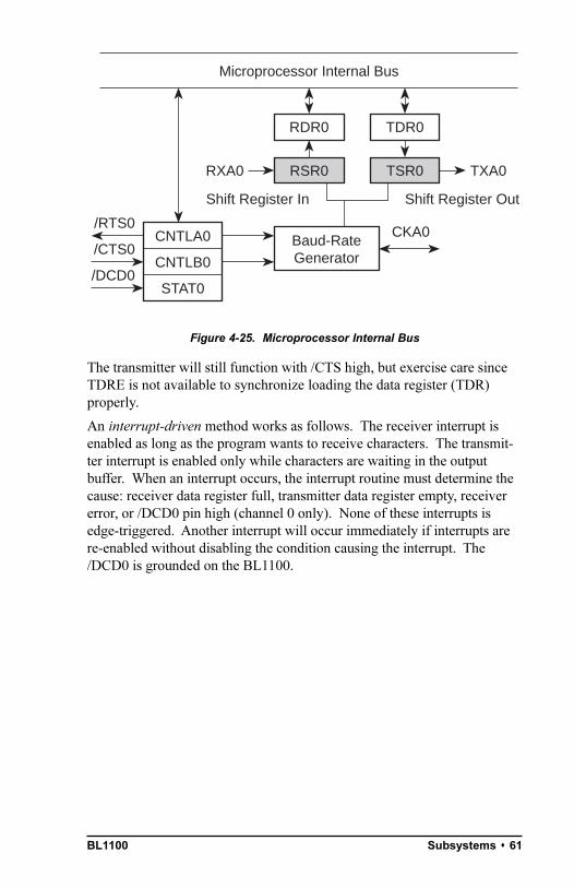
BL1100 Subsystems s 61
Figure 4-25. Microprocessor Internal Bus
The transmitter will still function with /CTS high, but exercise care sinceTDRE is not available to synchronize loading the data register (TDR)properly.
An interrupt-driven method works as follows. The receiver interrupt isenabled as long as the program wants to receive characters. The transmit-ter interrupt is enabled only while characters are waiting in the outputbuffer. When an interrupt occurs, the interrupt routine must determine thecause: receiver data register full, transmitter data register empty, receivererror, or /DCD0 pin high (channel 0 only). None of these interrupts isedge-triggered. Another interrupt will occur immediately if interrupts arere-enabled without disabling the condition causing the interrupt. The/DCD0 is grounded on the BL1100.
Microprocessor Internal Bus
RDR0 TDR0
TSR0RXA0 TXA0
Shift Register OutShift Register In
Baud-RateGenerator
CKA0CNTLA0
STAT0
CNTLB0
/RTS0
/CTS0
/DCD0
RSR0
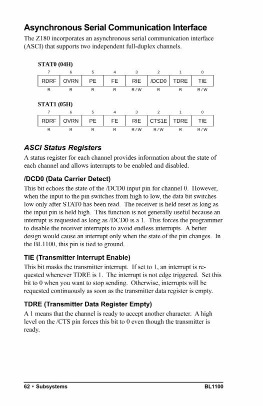
BL110062 s Subsystems
Asynchronous Serial Communication InterfaceThe Z180 incorporates an asynchronous serial communication interface(ASCI) that supports two independent full-duplex channels.
ASCI Status RegistersA status register for each channel provides information about the state ofeach channel and allows interrupts to be enabled and disabled.
/DCD0 (Data Carrier Detect)This bit echoes the state of the /DCD0 input pin for channel 0. However,when the input to the pin switches from high to low, the data bit switcheslow only after STAT0 has been read. The receiver is held reset as long asthe input pin is held high. This function is not generally useful because aninterrupt is requested as long as /DCD0 is a 1. This forces the programmerto disable the receiver interrupts to avoid endless interrupts. A betterdesign would cause an interrupt only when the state of the pin changes. Inthe BL1100, this pin is tied to ground.
TIE (Transmitter Interrupt Enable)This bit masks the transmitter interrupt. If set to 1, an interrupt is re-quested whenever TDRE is 1. The interrupt is not edge triggered. Set thisbit to 0 when you want to stop sending. Otherwise, interrupts will berequested continuously as soon as the transmitter data register is empty.
TDRE (Transmitter Data Register Empty)A 1 means that the channel is ready to accept another character. A highlevel on the /CTS pin forces this bit to 0 even though the transmitter isready.
STAT0 (04H)7 6 5 4 3 2 1 0
RDRF OVRN PE FE RIE /DCD0 TDRE TIE
R R R R R / W R R R / W
STAT1 (05H)7 6 5 4 3 2 1 0
RDRF OVRN PE FE RIE CTS1E TDRE TIE
R R R R R / W R / W R R / W

BL1100 Subsystems s 63
CTS1E (CTS enable, Channel 1)The signals RXS and CTS1 are multiplexed on the same pin. A 1 stored inthis bit selects the pin to serve the CTS1 function. A 0 selects the RXSfunction. (The RXS pin is the CSIO data receive pin.) When set to theRXS function, the CTS line has no effect. It is not advisable to use theCTS1 function on the BL1100, because the RXS line is needed to controlseveral other devices on the board.
RIE (Receiver Interrupt Enable)A 1 enables receiver interrupts and 0 disables them. A receiver interrupt isrequested on any of the following conditions: /DCD0 (channel 0 only),RDRF (receiver data register full), OVRN (overrun), PE (parity error), FE(framing error). The condition causing the interrupt must be removedbefore interrupts are re-enabled, or another interrupt will occur. Readingthe receiver data register (RDR) clears the RDRF flag. The EFR bit inCNTLA is used to clear the other error flags.
FE (Framing Error)A stop bit was missing, indicating scrambled data. This bit is cleared bythe EFR bit in CNTLA.
PE (Parity Error)Parity is tested only if MOD1 in CNTLA is set. This bit is cleared by theEFR bit in CNTLA.
OVRN (Overrun Error)Overrun occurs when bytes arrive faster than they can be read from thereceiver data register. The receiver shift register (RSR) and receiver dataregister (RDR) are both full.
RDRF (Receiver Data Register Full)This bit is set when data is transferred from the receiver shift register to thereceiver data register. It is always set when one of the error flags is set, inwhich case defective data are loaded to RDR. The bit is cleared when thereceiver data register is read, when the /DCD0 input pin is high, and byRESET and IOSTOP.
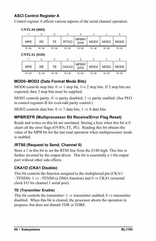
BL110064 s Subsystems
ASCI Control Register AControl register A affects various aspects of the serial channel operation.
MOD0MOD2 (Data Format Mode Bits)MOD0 controls stop bits: 0 Þ 1 stop bit, 1Þ 2 stop bits. If 2 stop bits areexpected, then 2 stop bits must be supplied.
MOD1 controls parity: 0 Þ parity disabled, 1 Þ parity enabled. (See PEOin control registers B for even/odd parity control.)
MOD2 controls data bits: 0 Þ 7 data bits, 1 Þ 8 data bits.
MPBR/EFR (Multiprocessor Bit Receive/Error Flag Reset)Reads and writes on this bit are unrelated. Storing a byte when this bit is 0clears all the error flags (OVRN, FE, PE). Reading this bit obtains thevalue of the MPB bit for the last read operation when multiprocessor modeis enabled.
/RTS0 (Request to Send, Channel 0)Store a 1 in this bit to set the RTS0 line from the Z180 high. This line isfurther inverted by the output driver. This bit is essentially a 1-bit outputport without other side effects.
CKA1D (CKA1 Disable)This bit controls the function assigned to the multiplexed pin (CKA1/TEND0): 1 Þ TEND0 (a DMA function) and 0 Þ CKA1 (externalclock I/O for channel 1 serial port).
TE (Transmitter Enable)
This bit controls the transmitter: 1 Þ transmitter enabled, 0 Þ transmitterdisabled. When this bit is cleared, the processor aborts the operation inprogress, but does not disturb TDR or TDRE.
CNTLA0 (00H)7 6 5 4 3 2 1 0
MPE RE TE /RTSOMPBR/
EFR MOD2 MOD1 MOD0
R / W R / W R / W R / W R / W R / W R / W R / W
CNTLA1 (01H)7 6 5 4 3 2 1 0
MPE RE TE CKA1DMPBR/
EFR MOD2 MOD1 MOD0
R / W R / W R / W R / W R / W R / W R / W R / W
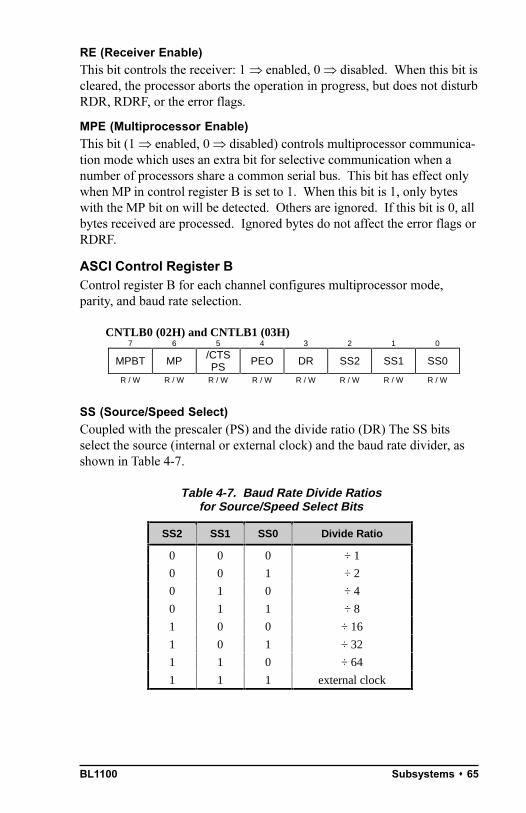
BL1100 Subsystems s 65
RE (Receiver Enable)
This bit controls the receiver: 1 Þ enabled, 0 Þ disabled. When this bit iscleared, the processor aborts the operation in progress, but does not disturbRDR, RDRF, or the error flags.
MPE (Multiprocessor Enable)
This bit (1 Þ enabled, 0 Þ disabled) controls multiprocessor communica-tion mode which uses an extra bit for selective communication when anumber of processors share a common serial bus. This bit has effect onlywhen MP in control register B is set to 1. When this bit is 1, only byteswith the MP bit on will be detected. Others are ignored. If this bit is 0, allbytes received are processed. Ignored bytes do not affect the error flags orRDRF.
ASCI Control Register BControl register B for each channel configures multiprocessor mode,parity, and baud rate selection.
SS (Source/Speed Select)
Coupled with the prescaler (PS) and the divide ratio (DR) The SS bitsselect the source (internal or external clock) and the baud rate divider, asshown in Table 4-7.
CNTLB0 (02H) and CNTLB1 (03H)7 6 5 4 3 2 1 0
MPBT MP /CTSPS PEO DR SS2 SS1 SS0
R / W R / W R / W R / W R / W R / W R / W R / W
Table 4-7. Baud Rate Divide Ratiosfor Source/Speed Select Bits
SS2 SS1 SS0 Divide Ratio
0 0 0 ÷ 1
0 0 1 ÷ 2
0 1 0 ÷ 4
0 1 1 ÷ 8
1 0 0 ÷ 16
1 0 1 ÷ 32
1 1 0 ÷ 64
1 1 1 external clock
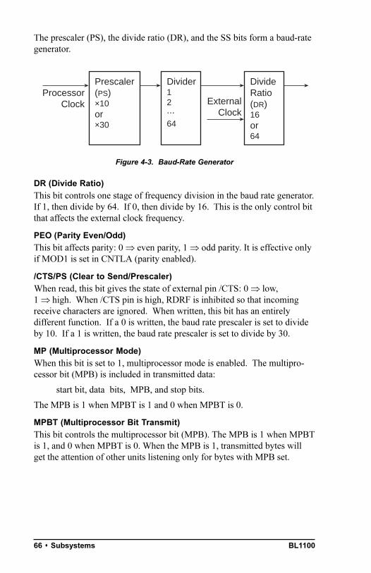
BL110066 s Subsystems
The prescaler (PS), the divide ratio (DR), and the SS bits form a baud-rategenerator.
Figure 4-3. Baud-Rate Generator
DR (Divide Ratio)
This bit controls one stage of frequency division in the baud rate generator.If 1, then divide by 64. If 0, then divide by 16. This is the only control bitthat affects the external clock frequency.
PEO (Parity Even/Odd)
This bit affects parity: 0 Þ even parity, 1 Þ odd parity. It is effective onlyif MOD1 is set in CNTLA (parity enabled).
/CTS/PS (Clear to Send/Prescaler)
When read, this bit gives the state of external pin /CTS: 0 Þ low,1 Þ high. When /CTS pin is high, RDRF is inhibited so that incomingreceive characters are ignored. When written, this bit has an entirelydifferent function. If a 0 is written, the baud rate prescaler is set to divideby 10. If a 1 is written, the baud rate prescaler is set to divide by 30.
MP (Multiprocessor Mode)
When this bit is set to 1, multiprocessor mode is enabled. The multipro-cessor bit (MPB) is included in transmitted data:
start bit, data bits, MPB, and stop bits.
The MPB is 1 when MPBT is 1 and 0 when MPBT is 0.
MPBT (Multiprocessor Bit Transmit)
This bit controls the multiprocessor bit (MPB). The MPB is 1 when MPBTis 1, and 0 when MPBT is 0. When the MPB is 1, transmitted bytes willget the attention of other units listening only for bytes with MPB set.
Prescaler(PS)×10or×30
ProcessorClock
Divider12...64
DivideRatio(DR)16or64
ExternalClock
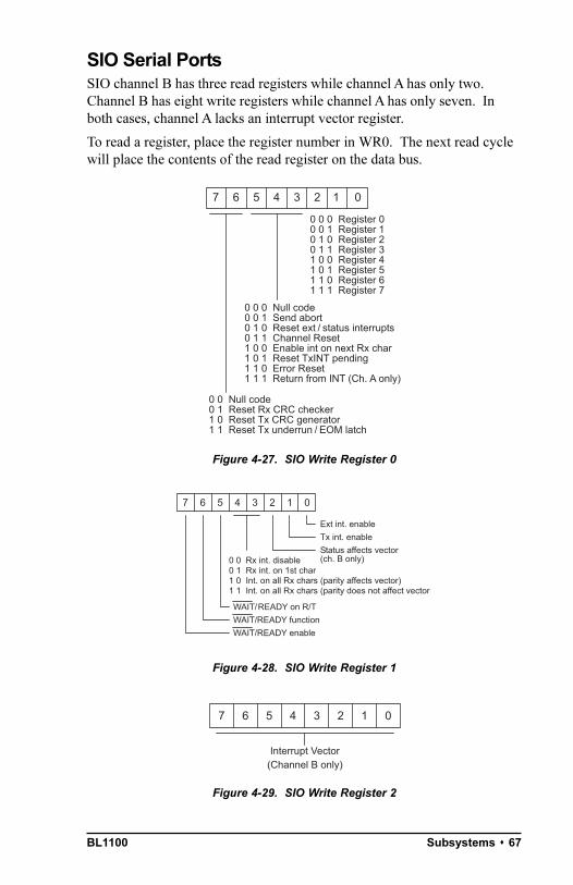
BL1100 Subsystems s 67
SIO Serial PortsSIO channel B has three read registers while channel A has only two.Channel B has eight write registers while channel A has only seven. Inboth cases, channel A lacks an interrupt vector register.
To read a register, place the register number in WR0. The next read cyclewill place the contents of the read register on the data bus.
Figure 4-27. SIO Write Register 0
Figure 4-28. SIO Write Register 1
Figure 4-29. SIO Write Register 2
Ext int. enable
07 6 5 4 3 2 1
0 0 Rx int. disable0 1 Rx int. on 1st char1 0 Int. on all Rx chars (parity affects vector)1 1 Int. on all Rx chars (parity does not affect vector
Tx int. enableStatus affects vector(ch. B only)
WAIT/READY on R/TWAIT/READY functionWAIT/READY enable
Interrupt Vector(Channel B only)
07 6 5 4 3 2 1
07 6 5 4 3 2 1
0 0 0 Register 00 0 1 Register 10 1 0 Register 20 1 1 Register 31 0 0 Register 41 0 1 Register 51 1 0 Register 61 1 1 Register 7
0 0 0 Null code0 0 1 Send abort0 1 0 Reset ext / status interrupts0 1 1 Channel Reset1 0 0 Enable int on next Rx char1 0 1 Reset TxINT pending1 1 0 Error Reset1 1 1 Return from INT (Ch. A only)
0 0 Null code0 1 Reset Rx CRC checker1 0 Reset Tx CRC generator1 1 Reset Tx underrun / EOM latch
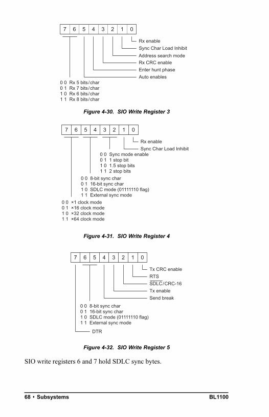
BL110068 s Subsystems
Figure 4-30. SIO Write Register 3
Figure 4-31. SIO Write Register 4
Figure 4-32. SIO Write Register 5
SIO write registers 6 and 7 hold SDLC sync bytes.
Rx enable
07 6 5 4 3 2 1
0 0 Rx 5 bits/char0 1 Rx 7 bits/char1 0 Rx 6 bits/char1 1 Rx 8 bits/char
Sync Char Load Inhibit
Address search modeRx CRC enable
Enter hunt phase
Auto enables
Rx enable
07 6 5 4 3 2 1
0 0 8-bit sync char0 1 16-bit sync char1 0 SDLC mode (01111110 flag)1 1 External sync mode
Sync Char Load Inhibit0 0 Sync mode enable0 1 1 stop bit1 0 1.5 stop bits1 1 2 stop bits
0 0 ×1 clock mode0 1 ×16 clock mode1 0 ×32 clock mode1 1 ×64 clock mode
Tx CRC enable
07 6 5 4 3 2 1
0 0 8-bit sync char0 1 16-bit sync char1 0 SDLC mode (01111110 flag)1 1 External sync mode
RTS
SDLC/CRC-16
Tx enable
Send break
DTR

BL1100 Subsystems s 69
Figure 4-33. SIO Read Register 0
Figure 4-34. SIO Read Register 1
Figure 4-35. SIO Read Register 2
The interrupt vector registers are automatically set from the Dynamic CEPROM when the BL1100 is booted. Write registers 6 and 7 are used toset the sync words for synchronous communications. (Set these to 0x7Efor SDLC.)
Certain SIO lines are shared with other functions on the BL1100. The SIOline /DCDB is used to input the voltage low signal (low when voltage islow). The SIO line /DTRB is used to hit the watchdog timer and ismanipulated by the function hitwd. If the RS-485 communication mode
Rx char available
07 6 5 4 3 2 1
Interrupt pending (Ch. A only)
Tx buffer empty
DCD
Sync/Hunt
CTS
Tx underrun/EOM
Break/Abort
Rx enable
07 6 5 4 3 2 1
Parity error
Rx overrun error
CRC/framing error
End of frame (SDLC)
0 0 0 2 80 0 1 0 60 1 0 0 40 1 1 0 81 0 0 0 31 0 1 0 71 1 0 0 51 1 1 1 8
I field bits inprevious byte
I field bits in 2ndprevious byte
Interrupt Vector(Channel B only)
07 6 5 4 3 2 1

BL110070 s Subsystems
is selected for Dynamic C programming, then SIO channel B is used forcommunication and cannot be used in the program being developed. SIOChannel B is also connected so that the NMI can be used instead of theregular mode 2 interrupt. This type of interrupt is used by Dynamic C inthe RS-485 communication mode, and allows the connection to bemaintained even if the target program disables interrupts for long periods.In this case, the NMI is shared for communications and power-fail warn-ing. When a NMI occurs, the interrupt routine determines whether thecause of the interrupt was a power failure by testing the /DCDB line to seeif power fail is activated.
If the Dynamic C 485 mode is not enabled, then all nonmaskable interruptsare transferred to the programmers NMI routine as defined by
#JUMP_VEC NMI_VEC name
Otherwise, only power-fail interrupts are dispatched to the programmersNMI service routine.
Since the hitwd function shares channel B with any other driver, a globallocation s0_wreg5 holds the contents of SIO Write Register 5 so thathitwd will not change any bits other than the DTR bit in this register.
If you decide to write a driver for SIO channel B using non-maskable interrupts, be aware that the NMI line into the micro-processor, once set, is latched until the condition causing theNMI is removed. Then a memory-write cycle occurs. Thisprevents multiple NMIs when reading the SIO registers.
The /WAIT/READY line from Channel A is connected to the DREQ1 lineof the Z180 microprocessor. This allows the DMA unit in the Z180 toperform high-speed input or output from SIO Channel A.
!
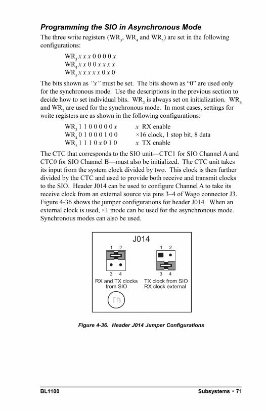
BL1100 Subsystems s 71
Programming the SIO in Asynchronous ModeThe three write registers (WR
3, WR
4 and WR
5) are set in the following
configurations:
WR3x x x 0 0 0 0 x
WR4x x 0 0 x x x x
WR5x x x x x 0 x 0
The bits shown as x must be set. The bits shown as 0 are used onlyfor the synchronous mode. Use the descriptions in the previous section todecide how to set individual bits. WR
2 is always set on initialization. WR
6
and WR7 are used for the synchronous mode. In most cases, settings for
write registers are as shown in the following configurations:
WR31 1 0 0 0 0 0 x x RX enable
WR40 1 0 0 0 1 0 0 ×16 clock, 1 stop bit, 8 data
WR51 1 1 0 x 0 1 0 x TX enable
The CTC that corresponds to the SIO unitCTC1 for SIO Channel A andCTC0 for SIO Channel Bmust also be initialized. The CTC unit takesits input from the system clock divided by two. This clock is then furtherdivided by the CTC and used to provide both receive and transmit clocksto the SIO. Header J014 can be used to configure Channel A to take itsreceive clock from an external source via pins 34 of Wago connector J3.Figure 4-36 shows the jumper configurations for header J014. When anexternal clock is used, ×1 mode can be used for the asynchronous mode.Synchronous modes can also be used.
Figure 4-36. Header J014 Jumper Configurations
J014
RX and TX clocksfrom SIO
TX clock from SIORX clock external
FD
1 2
3 4
1 2
3 4

BL110072 s Subsystems

BL1100 AnalogSection 73
CHAPTER 5: ANALOG SECTION
Chapter 5 provides information on the BL1100 A/D converter and analog I/O.
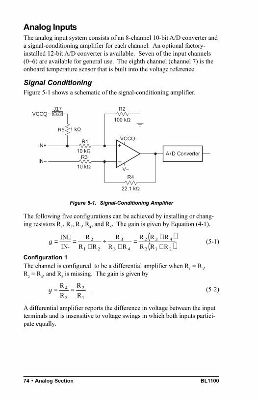
BL110074 s Analog Section
Analog InputsThe analog input system consists of an 8-channel 10-bit A/D converter anda signal-conditioning amplifier for each channel. An optional factory-installed 12-bit A/D converter is available. Seven of the input channels(06) are available for general use. The eighth channel (channel 7) is theonboard temperature sensor that is built into the voltage reference.
Signal ConditioningFigure 5-1 shows a schematic of the signal-conditioning amplifier.
Figure 5-1. Signal-Conditioning Amplifier
The following five configurations can be achieved by installing or chang-ing resistors R
1, R
2, R
3, R
4, and R
5. The gain is given by Equation (4-1).
Configuration 1
The channel is configured to be a differential amplifier when R1 = R
3,
R2 = R
4, and R
5 is missing. The gain is given by
A differential amplifier reports the difference in voltage between the inputterminals and is insensitive to voltage swings in which both inputs partici-pate equally.
R4
+
10 kΩIN+
IN10 kΩ
A/D Converter
R1
R3
22.1 kΩ
R2
R5
VCCQ
1 kΩ
100 kΩ
V–
VCCQJ17
( )( )213
432
43
3
21
2
RRR
RRR
RR
R
RR
R
-IN
IN
++
=+
÷+
=+
=g (5-1)
.R
R
R
R
1
2
3
4 ==g (5-2)

BL1100 AnalogSection s 75
Configuration 2
The channel is configured to be a noninverting single-ended amplifier whenR
5 is missing. Input IN is connected to ground. Input IN+ is sampled.
R2 is either missing or is a large value such as 100 kW. The gain is given by
The input impedance is very high when R2 is missing. Otherwise, theinput impedance is R
1 + R
2.
Configuration 3
The channel is an inverting single-ended amplifier when R5 is missing.
Input IN is sampled and input IN+ is connected to ground. The gain isgiven by
R2 can be missing without affecting the operation. If R
2 is present, input
IN+ may be left unconnected.
Configuration 4
The channel measures resistance, where R is the unknown resistance acrossIN+ and IN. Input IN is connected to ground. R is given by
where V is the voltage at IN+. The gain from the input IN+ pin is the sameas for Configuration 2 above. The reference (REF) can be the 2.5 Vprecision reference U6 (LT1019) or the +5 V power supply if less accuracyis needed. The ability of the reference to deliver current is limited toapproximately 8 mA. Thus, the +5 V power supply or an external sourcemust be used for low resistances. If +5 V is used, another channel can beused to track the voltage level, which is only regulated to a few percent.
Configuration 5
The channel measures current, where R, the resistance placed between IN+and IN is known, and the current passing through R, which is given byi = V/R, will be measured. The setup is similar to Configuration 4.
.1R
R
R
RR
3
4
3
43 +=+
=g (5-3)
.R
R
3
4=g (5-4)
,V
VREFR 5
−=R (5-5)
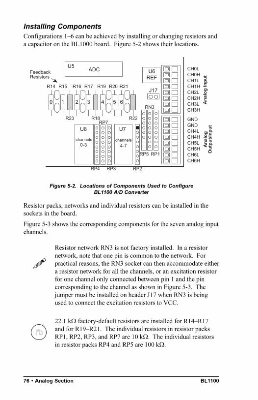
BL110076 s Analog Section
Installing ComponentsConfigurations 16 can be achieved by installing or changing resistors anda capacitor on the BL1000 board. Figure 5-2 shows their locations.
Figure 5-2. Locations of Components Used to ConfigureBL1100 A/D Converter
Resistor packs, networks and individual resistors can be installed in thesockets in the board.
Figure 5-3 shows the corresponding components for the seven analog inputchannels.
Resistor network RN3 is not factory installed. In a resistornetwork, note that one pin is common to the network. Forpractical reasons, the RN3 socket can then accommodate eithera resistor network for all the channels, or an excitation resistorfor one channel only connected between pin 1 and the pincorresponding to the channel as shown in Figure 5-3. Thejumper must be installed on header J17 when RN3 is beingused to connect the excitation resistors to VCC.
22.1 kW factory-default resistors are installed for R14R17and for R19R21. The individual resistors in resistor packsRP1, RP2, RP3, and RP7 are 10 kW. The individual resistorsin resistor packs RP4 and RP5 are 100 kW.
54320 1
ADC
GNDGNDCH4LCH4HCH5LCH5HCH6LCH6H
CH1LCH1HCH2LCH2HCH3LCH3H
CH0LCH0H
J17
RN3
RP5 RP1
U8
channels0-3
U7
channels4-7
RP4
R14
6
R15 R16 R17 R19 R21R20
R22R18R23
FeedbackResistors
U6REF
RP3
RP7
RP2
An
alo
g In
pu
tA
nal
og
Ou
tpu
t/In
pu
t
U5
!
FD

BL1100 AnalogSection s 77
+
IN+
INA/D Converter
RP1A
RP7A
VCCQ
V–
VCCQJ17
54321
J17
RN3
R14
60
1
4
112
321
1 2
21
RP4A
1
2
12
R14
RN3
U8A
RP7ARP4ARP1A
(a) Channel 0
Figure 5-3. Analog Input Channel Configuration
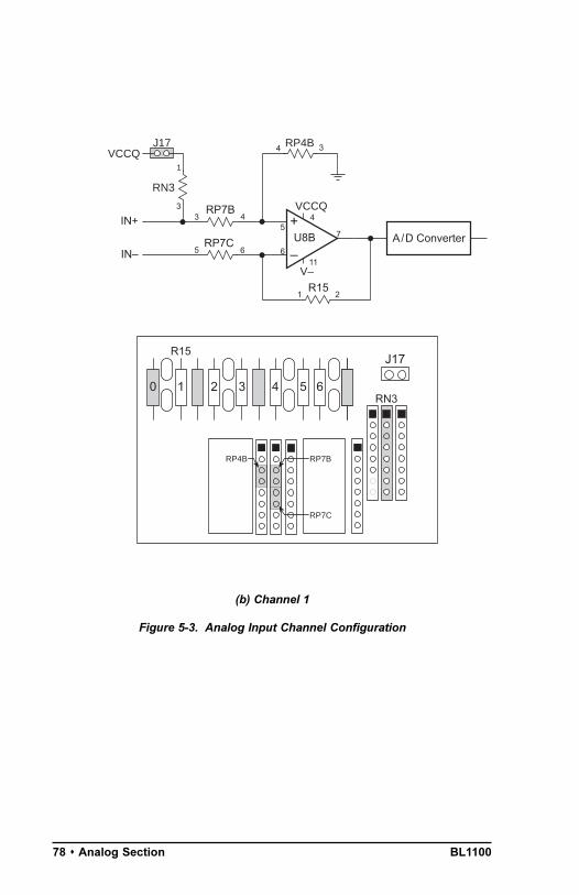
BL110078 s Analog Section
+
IN+
INA/D Converter
RP7B
RP7C
VCCQ
V–
VCCQJ17
54321
J17
RN3
R15
60
7
4
116
543
5 6
21
RP4B
1
3
34
R15
RN3
RP7C
U8B
RP7BRP4B
(b) Channel 1
Figure 5-3. Analog Input Channel Configuration

BL1100 AnalogSection s 79
+
IN+
INA/D Converter
RP2A
RP2B
VCCQ
V–
VCCQJ17
54321
J17
RN3
R16
60
8
4
119
1021
3 4
21
RP4C
1
4
56
R16
RN3
RP2B
U8C
RP2A
RP4C
(c) Channel 2
Figure 5-3. Analog Input Channel Configuration
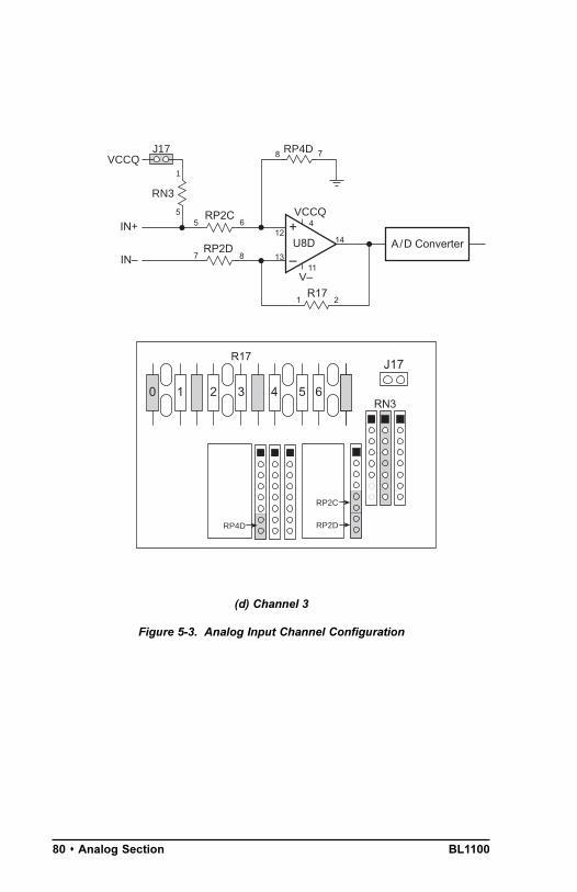
BL110080 s Analog Section
+
IN+
INA/D Converter
RP2C
RP2D
VCCQ
V–
VCCQJ17
54321
J17
RN3
R17
60
14
4
1113
1265
7 8
21
RP4D
1
5
78
R17
RN3
RP2DRP4D
U8D
RP2C
(d) Channel 3
Figure 5-3. Analog Input Channel Configuration
BL1100 AnalogSection s 81
+
IN+
INA/D Converter
RP3B
RP3A
VCCQ
V–
VCCQJ17
54321
J17
RN3
R19
60
1
4
112
343
2 1
21
RP5A
1
6
12
R19
RN3
RP5A
U7A
RP3B
RP3A
(e) Channel 4
Figure 5-3. Analog Input Channel Configuration
BL110082 s Analog Section
+
IN+
INA/D Converter
RP3C
RP3D
VCCQ
V–
VCCQJ17
54321
J17
RN3
R20
60
7
4
116
556
7 8
21
RP5B
1
7
34
R20
RN3
RP5B
U7B
RP3C
RP3A
RP3D
(f) Channel 5
Figure 5-3. Analog Input Channel Configuration
BL1100 AnalogSection s 83
+
IN+
INA/D Converter
RP1C
RP1D
VCCQ
V–
VCCQJ17
54321
J17
RN3
R21
60
8
4
119
1065
8 7
21
RP5C
1
8
56
R21
RN3
U7C
RP5C
RP1D
RP1C
(g) Channel 6
Figure 5-3. Analog Input Channel Configuration

BL110084 s Analog Section
Table 5-1. Op-Amp Specifications
AmplifierParameter
LM324 LT1014
Maximum Input Offset (µV) 7000 250
Maximum Input Offset Drift (µV/°C) 30 2
A/D ConversionThe eight amplifier channels feed into the A/D converter. Channel 7 isused to measure the temperature signal generated by the LTC1019 refer-ence chip at U6. Channel 6 can also be used as a buffer to provide anexternal reference voltage.
To use Channel 6 as a buffer, the J5 Wago connector must bereplaced with a header.
The A/D converter is a single-chip Linear Technology LTC1094 (10 bits at120 µs) or LTC1294 (12 bits at 120 µs).
Sources of ErrorThe operational amplifiers (U7 and U8) used in the analog input sectioncan be either a National Semiconductor LM324 or, for more precision, aLinear Technology LT1014. Table 5-1 compares the performance of thesetwo op-amps.
The LM324 amplifiers will serve many purposes. However, the better-quality LT1014 amplifiers are needed for measuring low voltages, such asthose associated with thermocouples.
The input offset appears as a nonexistent voltage amplified by the gain ofthe amplifier. This offset is tested and recorded in the EEPROM for eachamplifier, and can be used to correct the measurements. However,temperature drift gives an additional offset that is difficult to correct.
The LT1019, used by the A/D as an absolute voltage reference, has amaximum error of 0.2 percent (0.05 percent for the LT1019A). There aresmall errors in the reference voltage related to temperature and load.
The A/D circuitry has errors relating to linearity, offset, noise, drift, andgain amounting to a few least significant bits. The offset and gain can becompensated easily. Noise can be minimized by averaging many measure-ments. Averaging four times as many measurements cuts the noise in half.Linearity and drift errors are more difficult to correct, but should be nomore than one-half of the least-significant bit.
!

BL1100 AnalogSection s 85
Onboard Temperature SensorThe LT1019 voltage reference at U6 on the BL1100 board generates anoutput voltage proportional to the temperature of its internal silicon die.This voltage is related to the temperature by the approximate relationship
V = 0.0021 × T , (5-6)
where V is the voltage in volts and T is the temperature in kelvins [T(K) =T(°C) + 273]. The temperature-dependent voltage is connected to analoginput channel 7 as shown in Figure 5-4.
Figure 5-4. Signal Conditioning Circuit for OnboardTemperature Measurement
The equivalent voltage for the resistor divider is given by
Substituting the values shown in Figure 5-4,
VE = (2.5 V) × [(430 W)/(430 W + 2000 W)] = 0.442 V .
The equivalent voltage for the resistor divider is given by
Substituting the values shown in Figure 5-4,
RE = 1/[(1/430 W) + (1/2000 W)] = 354 W .
+
To A/D Converter
LT1019
2 kΩRP1B
10 kΩ
+2.5 V ref
+2.5 Vref
430 Ω
+5 V
5 V
10 kΩRP7D U7D
R22
49.9 kΩ
R23
R18
(5-7).R23R18
R18VV REFE
+=
(5-8).
R23
1
18R
1
1R E
+
=

BL110086 s Analog Section
Both op-amp inputs will be at the voltage VTEMP
. The current through RE
and RP7D must equal the current through R22. This leads to the equation
or
VTEMP
= 0.172 × VOUT
+ 0.366 V . (5-9)
Typically, the LT1019 heats itself about 2°C to 6°C above the ambienttemperature, depending on the size of the load driven by the referenceoutput. The entire enclosure containing the BL1100 may be additionallyheated, so caution must be used in interpreting the temperature calculated.The actual temperature in degrees Celsius can then be calculated from
The offset is typically 4°C to allow for self-heating and TCOEF
is stored inthe EEPROM as a calibration value for each particular LT1019 tempera-ture reference chip. T
COEF is based on a voltage coefficient of 0.0021 V/°C.
An error in the temperature is an error in the coefficient andnot a temperature offset, except for the offset due to self-heating.
The LT1019 temperature sensor can be used to record temperature overtime, to measure ambient temperature, or to measure the cold-junctiontemperature in thermocouples. The temperature sensor is placed close tothe field wiring connectors to minimize the thermal path between the chipand the cold junctions.
Appendix G provides sample applications for the analog inputsand A/D conversion.
Ω
−=
Ω
−00050
VV
35410
V442.0V TEMPOUTTEMP
(5-10).273-offsetT
V T
COEF
TEMP −
=
!
$

BL1100 AnalogSection s 87
Analog OutputAn optional Maxim AD7543 D/A converter (DAC) chip may be installedon the BL1100 in socket U12. A Maxim OP07 op-amp buffer must also beinstalled in socket U19, and a National LM285 voltage reference must beinstalled in socket Z1. Figure 5-5 illustrates the locations of these compo-nents.
Figure 5-5. Locations of DAC Components
The DAC output is routed through header J28 to connector J5 pin 1. If J28pins 12 are jumpered, then the board is set up for DAC output of up to2 mA at 0 V to 2.5 V on Wago connector J5. If J28 pins 23 are jumpered,then J5 pin 1 will be a ground and the DAC output will not be sent to J5.Figure 5-6 summarizes these configurations.
Figure 5-6. Header J28 Jumper Settings
R3
ADC
DAC
Buffer
J5
Ana
log
Inpu
tA
nalo
gO
utpu
t/Inp
ut
Z1
RA
M
J4
A5E-0104M
U12
U19
C012J28
U5
No DACinstalled
FD
1 2 3
J28
GNDGNDCH4LCH4HCH5LCH5HCH6LCH6H
An
alo
gO
utp
ut/
Inp
ut
J5
DAC output enabled
1 2 3
J28
GNDCH4LCH4HCH5LCH5HCH6LCH6H
An
alo
gO
utp
ut/
Inp
ut
J5AOUT

BL110088 s Analog Section

BL1100 Software Reference 89
CHAPTER 6: SOFTWARE REFERENCE
Chapter 6 describes the software functions available for the BL1100.This chapter covers the following topics.• Supplied Software• Digital Interfaces• A/D Converter• D/A converter• Miscellaneous Drivers

BL110090 s Software Reference
Supplied SoftwareSoftware drivers for controlling the BL1100s inputs/outputs are providedwith Dynamic C. The library BL11XX.LIB provides drivers specific to theBL1100. The BL11XX.LIB library is automatically included when aDynamic C connection is initiated to a BL1100 in program mode. For theother libraries, it is necessary to include the appropriate Dynamic Clibraries in your program. Table 6-1 lists the libraries for the BL1100.
An AASC library does not exist at this time for SIO Port B.The AASCSIOA.LIB library may be used be replacing A with B.
Either the AASC libraries or the libraries listed after BL11XX.LIB inTable 6-1 need to be included in your program if the serial ports are beinused. To include these libraries, use the #use directive as shown below.
#use aasc.lib
See the Dynamic C Technical Reference and the Dynamic CFunction Reference manuals for more information on #useand other directives, as well as the serial communicationlibraries.
Table 6-1. BL1100 Software Libraries
Library Application
AASC.LIB All BL1100 serial communication applications
AASCSIOA.LIB AASC drivers for SIO Port A
AASCZ0.LIB AASC drivers for Z180 ZIO Port 0
AASCZ1.LIB AASC drivers for Z180 ZIO Port 1
BL11XX.LIB All BL1100 applications
NETWORK.LIB Utilities for half-duplex RS-485 communication
S0232.LIB RS-232 drivers for SIO Port A
S1232.LIB RS-232 drivers for SIO Port B
Z0232.LIB RS-232 drivers for Z180 ZIO Port 0
Z1232.LIB RS-232 drivers for Z180 ZIO Port 1
$
!
BL1100 Software Reference s 91
Digital Interfaces
KIO Counter/Timer Circuit (CTC)The following function initializes the CTC.
void setctc( char ctc, char mode, char timer,char intr )
PARAMETERS: ctc is the CTC unit (03)
mode 0timer mode sysclock/16, triggers immediately1timer mode sysclock/256, triggers immediately2counter runs off external clock4timer mode sysclock/16 triggers on rising edge of /CLK5timer mode sysclock/256 triggers on rising edge of /CLK6timer mode sysclock/16 triggers on falling edge of /CLK7timer mode sysclock/256 triggers on falling edge of /CLK
timer is the timer reload value (0255)
intr 0disables interrupt1enables interrupt
LIBRARY: BL11XX.LIB
The following code could be used to start the timer and enter an interruptroutine every 5 ms.
#INT_VEC CTC2_VEC myroutine
setctc( 2,1,180,1 ); // every 5 milliseconds
The sanple program CTCDEMO.C demonstrates the operation of the CTCand the setctc function.
The following interrupt service routine will divide the period by anadditional factor of up to 256. The routine executes in about 10 µs.
char timer;
#INT_VEC CTC2_VEC ctc_interrupt#asm
ctc_interrupt:: push af push hl ld hl,timer dec (hl) jr z,ctc_2 pop hl pop af ei reti
ctd_2: continue interrupt routine
#endasm

BL110092 s Software Reference
High-Current/High-Voltage DriverThe following functions provide access to the 5841A high-voltage driver.Remember that the order of the output bits (on Wago connector J101) isreversed. OUT8 is bit 0 (its mask is 0x01) and OUT1 is bit 7 (0x80).
void hv_wr( char value )
Writes the byte value to the driver. The output enable remains thesame. Note that all 8 bits are strobed to the output register in oneclock, so all bits change simultaneously. A 1 enables the correspondingoutput (pulls low). A 0 disables the corresponding output.
LIBRARY: DRIVERS.LIB
This function uses the Z180 CSI/O serial interface to transmitone byte to the high-voltage driver chip. It can conflict withdrivers for the A/D converter if either is used in interruptroutines at different priority level.
void hv_enb()
Enables the high-voltage driver chip.
LIBRARY: DRIVERS.LIB
void hv_dis()
Disable the high-voltage driver chip.
LIBRARY: DRIVERS.LIB
!
BL1100 Software Reference s 93
Liquid Crystal Display InterfaceThe following functions from the DRIVERS.LIB library drive a 4 ×20LCD such as the Optrex DMC20481.
void lcd_init ( int mode )
Initializes the display. Under normal circumstances, mode should be0x18.
int lputc( int ch )
Sends one character to the display. Special characters can be sent tocontrol the display. These characters all have bit 7 set to 1.
\xF0 clear line 1
\xF1 clear line 2
\xF2 cursor off, stop cursor blink
\xF3 cursor on
\xF4 cursor to blinking mode
\xF5 shift display left
\xF6 shift display right
\x80 codes 80, 81, etc. position cursor atcolumn 0, 1, etc. on line 0
\xC0 codes C0, C1, etc. position cursor atcolumn 0, 1, etc. on line 1
\n position cursor to first column of secondline
char *lputs( char *string )
Sends a null-terminated string to the LCD.
int lprintf( char *,... )
lprintf() is the same as printf with output to the LCD driver.
These functions can be easily modified for displays with other formatssuch as 4 × 40 characters.
BL110094 s Software Reference
A/D ConverterThe following functions work for either the 10-bit converter or the 12-bitconverter as noted.
int ad_rd( int channel )
Reads the 10-bit LTC1094 by calling ad_rd10.
int ad_rd10 (int channel)
Reads the 10-bit LTC1094 A/D converter.
PARAMETERS: The low three bits of channel specify the channelnumber (07); the fourth bit must be 0 for bipolar mode, or 1 forunipolar mode. For the unipolar mode, add 8 to the channel number.
RETURN VALUE: The return value is shifted left by 2 bits, so itappears as a 12-bit number.
The function returns a number from 2048 to +2047 for thebipolar mode. This is the output from the A/D converter andcorresponds to a range of 2.5 V to +2.499 V. The least two bitsof the returned value are always zero.
In unipolar mode, the function returns a number in the range from0 to 4095, corresponding to a range of 0 V to 2.499 V.
The function returns 32768 if an error occurs.
LIBRARY: BL11XX.LIB
int ad_rd12( int channel )
Reads the 12-bit LTC1294 A/D converter. The function is basically thesame as ad_rd10, but it applies to the 12-bit converter and the leasttwo bits of the return result have value.
Approximately 120 µs are required to acquire a sample from the LTC1094and LTC1294 chips. Interrupts are disabled during the sampling unless nointerrupts are defined with #define NODISINT.
Temperature MeasurementsThe sample program BDTEMP.C in the Dynamic C SAMPLES subdirectoryprovides functions for testing the type of A/D converter, setting tempera-ture coefficient, and reading the temrperature from the onboard tempera-ture reference. The following functions are used and defined inBDTEMP.C.

BL1100 Software Reference s 95
int bdtemp()
Returns the temperature in degrees Celsius:
float bdtemp_init()
Must be called before bdtemp can be called.
bdtemp
Returns the temperature in units of 0.1°C. If bdtemp returns that thecoefficient in EEPROM is bad, bdtemp takes an error exit.
settemp()
Sets the EEPROM coefficient.
setad
Tries to determine the type of A/D converter on board based oncharacteristic return values from reading the temperature sensor.
High-Speed SamplingThe following function collects samples using the 10-bit LTC1094 A/Dconverter at uniform intervals at sampling rates up to 12,800 samples persecond.
int ad_rd10s( int chan, int count,int *buf, unsigned int divider )
Samples data from the Little Giant A/D converter at uniform intervals.This function uses Z180 programmable reload timer (PRT) number 1.Interrupts are disabled for the entire time the buffer of samples is beingacquired, unless #define NODISINT is defined.
PARAMETERS: chan is the channel number (07), plus 8 for theunipolar mode (otherwise the bipolar mode is assumed).
count specifies the number of samples to collect.
buf points to a buffer where data is stored.
divider determines the sample rate based on sample rate = clock/(20 × divider). divider should not be smaller than 36, which yields12,800 samples per second with a 9.216 MHz clock.
RETURN VALUE: 1 for no error, or 0 indicating that a sample wasmissed. The function can miss a sample if the divider is too small or aninterrupt occurs during sampling. Interrupts during sampling willdisrupt the uniformity of the sampling.
LIBRARY: BL11XX.LIB

BL110096 s Software Reference
D/A Converter int wdac( int value )
Writes a 12-bit digital value to the DAC.
PARAMETER: value is between 0 and 4095 for output voltagesbetween 0 V and 2.499 V (nominal). For accurate work, apply asoftware gain adjustment since the voltage reference is subject to up to80 counts of error and the DAC can have as many as 15 counts gainerror. With correction, the DAC should operate with 12 bit accuracyover range and temperature.
Miscellaneous Drivers
Time/Date ClockThe battery-backed real-time clock is based on the Epson 72421 chip. The72421A is accurate to approximately one second per day. The 73421B isaccurate to approximately five seconds per day. Time values are resolvedto one second and extend up to 80 years in the future. A Dynamic Csample program, SETCLOCK.C, is provided to read and write from/to theclock chip. The lithium battery should keep the clock going for about 10years unless the board is stored at high temperatures for long periods withthe power off.
Time/Date FunctionsDate/time functions can be found in DRIVERS.LIB. Also, the sampleprogram SETCLOCK.C provides a keyboard interface to display and set thedate/time clock.
The following structure is defined to hold the date and time.
struct byte tm_sec; // seconds 0-59byte tm_min; // minutes 0-59byte tm_hour; // 24-hour time 0-23byte tm_mday; // day of month 1-31byte tm_mon; // month 1-12byte tm_year; // 90=1990, 101=2001byte tm_wday; // 0=Sun...6=Sat
tm;
Time can also be expressed as seconds since January 1, 1980 (i.e.,midnight December 31, 1979).
The following functions in DRIVERS.LIB are provided to read the date/time clock. Note that it takes about 600 µs to read the clock chip.

BL1100 Software Reference s 97
int tm_rd( struct tm *value )
Reads the real-time clock. Returns 0 if successful, or 1 otherwise.The date/time value is passed back in *value.
unsigned long clock()
Reads the 72421 timer and returns the time as seconds since January 1, 1980.
int tm_wr( struct tm *value )
Writes the date and time, passed in *value, to the clock. Returns 0 ifsuccessful, and 1 otherwise.
unsigned long mktime( struct tm *value )
Converts time, passed as *value, into time expressed as seconds sinceJanuary 1, 1980. Does not access the timer chip.
int mktm( struct tm *value, long time )
Converts time, expressed as seconds since January 1, 1980, into thestructure *value. Does not access timer chip.
Watchdog TimerThe watchdog timer is a reliability feature. If the watchdog timer isenabled by connecting a jumper across header J22, a timer starts runningand is reset by calling the library function hitwd(). When the timer runsfor 1.6 seconds without being reset, the watchdog times out. The timeoutforces the BL1100 into a hardware reset condition for 50 ms, then theboard resumes operation as if the power had just been turned on. It ispossible to distinguish between a power-on reset and a watchdog reset.While debugging under Dynamic C, the watchdog is automatically hitfrequently. However, if a program starts to run without any watchdoghits, and jumper J22 is connected, a reset will take place and Dynamic Cwill report a loss of communication.
void hitwd()
Hits the watchdog timer. A hit resets the timer counter, whichpostpones a hardware reset for another 1.6 seconds.
int wderror()
Returns non-zero if the watchdog timer caused the most recent reset. Ifthe reset was caused by either turning the power on or by pushing thereset pushbutton, then the function returns zero.
The watchdog timers purpose is to provide recovery from a fault condi-tion, such as an endless loop or an invalid microprocessor state. Such afault can be caused by an electrical transient or by a software bug. Anelectrical transient can generate a microprocessor state that would beimpossible during normal operation. A transient effect strong enough to
BL110098 s Software Reference
upset the state of the microprocessor or erase part of the memory can bemuch weaker than that needed to cause permanent damage. The ability torecover from such faults improves system reliability under stressfulenvironmental conditions.
Software bugs that only occur once a week or once a year and cause theprogram to enter an endless loop are not unusual, but are difficult tocorrect. The following three scenarios could result from a softwaremalfunction or electrical interference.
1. The stack overflows only when a rare sequence of events takes place(such as an interrupt when a seldom executed, deeply nested piece ofcode is executing). If that code is executed for only 10 µs every 5 min,and the interrupts take place on the average only once every hour, thenthe program will probably crash about once a year.
2. A multi-byte variable is shared between a high-level function and aninterrupt service routine, and proper precautions are not taken toprevent interrupts while the high-level function modifies the variable.If the store to the multi-byte variable is interrupted before all of itsbytes have been stored, the interrupt routine will see a mixture of theold and new values, or garbage. Dynamic C provides a shared keywordto prevent this.
3. Software may not anticipate catastrophic conditions. For example, afunction that processes an A/D conversion value may always expect apositive value. However, if an electrical transient occurs when anearby motor starts (which may happen only once a day) and makes thevalue of the A/D conversion negative, the program might enter anendless loop. The programmer is unlikely to find the error throughtesting.
Take care to prevent a state that will include hitwd() in anendless loop. The watchdog will not time out and reset thesystem.
!

BL1100 Troubleshooting 99
APPENDIX A: TROUBLESHOOTING
Appendix A provides procedures for troubleshooting system hardware andsoftware.

BL1100100 s Troubleshooting
Out of the BoxCheck the items mentioned in this section before starting development.
Verify that the BL1100 runs in standalone mode before connecting anyexpansion boards or I/O devices.
Verify that the entire host system has good, low-impedance, separategrounds for analog and digital signals. Often the BL1100 is connectedbetween the host PC and another device. Any differences in groundpotential from unit to unit can cause serious problems that are hard todiagnose.
Do not connect analog ground to digital ground anywhere.
Double-check the connecting ribbon cables to ensure that all wires goto the correct screw terminals on the BL1100.
Verify that the host PCs COM port works by connecting a good serialdevice to the COM port. Remember that COM1/COM3 and COM2/COM4 share interrupts on a PC. User shells and mouse drivers, inparticular, often interfere with proper COM port operation. Forexample, a mouse running on COM1 can preclude running Dynamic C onCOM3.
Use the supplied Z-World power supply. If another power supply mustbe used, verify that it has enough capacity and filtering to support theBL1100.
Use the supplied Z-World cables. The most common fault of user-made cables is failure to properly assert CTS at the RS-232 port of theBL1100. Without CTSs being asserted, the BL1100s RS-232 port willnot transmit. Assert CTS by either connecting the RTS signal of thePCs COM port or looping back the BL1100s RTS.
Experiment with each peripheral device connected to the BL1100 todetermine how it appears to the BL1100 when powered up, powereddown, and/or when its connecting wiring is open or shorted.
Dynamic C Will Not StartIn most situations, when Dynamic C will not start, an error messageannouncing a communication failure will be displayed. The following listdescribes situations causing an error message and possible resolutions.
Wrong Baud Rate Make sure the jumpers are set correctly for thedesired baud rate. Headers J10, J12, and J25 all affect the baud rate..
Wrong Communication Mode Both sides must be talking RS-232(header J7) or RS-485 (header J9), depending on which protocol isbeing used.
Wrong COM Port A PC generally has two serial ports, COM1 andCOM2. Specify the one being used in the Dynamic C Target Setupmenu. Use trial and error, if necessary.
BL1100 Troubleshooting s 101
Wrong Operating Mode Communication with Dynamic C will belost if the BL1100 is set for the run mode. Reconfigure the board forprogramming mode.
Wrong Memory Size Jumpered pins on headers J16 and J20 specifyEPROM size. Verify EPROM size configuration with Figure 3-10.
SRAM and EPROM installed Both the SRAM and EPROM chipsmust be installed in sockets U10 and U011.
If all else fails, connect the serial cable to the BL1100 after power up. Ifthe PCs RS-232 port supplies a large current (most commonly on portableand industrial PCs), some RS-232 level converter ICs go into a nonde-structive latch-up. Connect the RS-232 cable after power up to eliminatethis problem.
Dynamic C Loses Serial LinkIf the program disables interrupts for a period greater than 50 milliseconds,Dynamic C will lose its serial link with the application program. Makesure that interrupts are not disabled for a period greater than 50 millisec-onds.
BL1100 Repeatedly ResetsThe BL1100 resets every 1.0 seconds if the watchdog timer is not hit. Ifa program does not hit the watchdog timer, then the program will havetrouble running in standalone mode. To hit the watchdog, make a call tothe Dynamic C library function hitwd.
PIO ProblemsPIO Modes 0, 1, and 2 need a strobe to transfer the data. The strobe linesare connected to header J12. Use Mode 3 for static input. Mode 1 canappear to work for static input, but results will be erratic since the strobeline is floating.
Power-Supply ProblemsThe linear power supply regulator will overheat when digital input voltagesabove 15 V are present on the BL1110 and BL1120. Keep the digital inputvoltages below 28 V for the BL1100 with a switching power supply regula-tor
If the external power supply does not have sufficient capacity, an addi-tional load such as an LED can trigger a power-fail interrupt, initiating ahardware reset. The reset triggers the load to be turned off, but then thecomputer restarts and turns the load back on. The oscillation can becorrected by increasing the size of the power supply.

BL1100102 s Troubleshooting
Blown-Out 5841 Driver ChipThe 5841 driver chip may blow if SUB floats. Protect the chip by install-ing a filter capacitor in the line connecting K to the power supply if thiswire is long.
If K is not connected, the 5841 chip will blow if an inductive load isconnected. The circuit will then be enabled, so be sure to plan for thissituation.
Common Programming Errors Values for constants or variables out of range. Table A-1 lists accept-
able ranges for variables and constants.
Mismatched types. For example, the literal constant 3293 is of typeint (16-bit integer). However, the literal constant 3293.0 is of typefloat. Although Dynamic C can handle some type mismatches,avoiding type mismatches is the best practice.
Counting up from, or down to, one instead of zero. In software, ordinalseries often begin or terminate with zero, not one.
Confusing a functions definition with an instance of its use in a listing.
Not ending statements with semicolons.
Not inserting commas as required in functions parameter lists.
Leaving out ASCII space character between characters forming adifferent legalbut unwantedoperator.
Confusing similar-looking operators such as && with &, == with =, and// with /.
Inadvertently inserting ASCII nonprinting characters into a source-codefile.
Table A-1. Constant and Variable Ranges
Type Range
int –32,768 (–215) to+32,767 (215 – 1)
long int −2,147,483,648 (−231) to+2147483647 (231 − 1)
float 1.18 × 10−38 to3.40 × 1038
char 0 to 255

BL1100 Specifications 103
APPENDIX B: SPECIFICATIONS
Appendix B provides comprehensive BL1100 physical, electronic andenvironmental specifications.

BL1100104 s Specifications
Table B-1. BL1100 General Specifications
Parameter Specification
Board Size5.6" × 4.8" × 1.2"(142 mm × 122 mm × 30 mm)
Operating Temperature -40°C to 70°C, may be stored at –55°C to 85°C
Humidity 5% to 95%, noncondensing
Power9 V DC to 28 V DC (BL1100), 80 mA at 24 V,switching regulator; 9 V to 15 V for linear regulator
Configurable I/O16, 5 V TTL and CMOS compatible (I/O lines aresoftware-selectable as either inputs or outputs)
Digital I/O See Configurable I/O
Digital OutputsEight high-current channels, one channel can sinkup to 500 mA continuously at 25°C, 8 channels cansink up to 165 mA each at 50°C and 48 V DC
Analog InputsSeven 10-bit conditioned: default differential inputis 0 V to 0.8 V for voltage range of –4.3 V to 4.3 V
Analog Outputs One optional, 2 mA at 0 V to 2.5 V
ResistanceMeasurement Input
No
Processor Z180
Clock 9.216 MHz (12.288 MHz optional)
SRAM 32K standard, supports up to 512K
EPROM 32K standard, supports up to 512K
Flash EPROM No
EEPROM 512 bytes
Counter/Timers Two in hardware, four in software
Serial PortsTwo RS-232 (with CTS/RTS) andtwo full-duplex RS-485
Serial Rate Up to 57,600 bps
Watchdog Yes
Time/Date Clock Yes
Backup BatteryPanasonic BR2325-1HG 3 V DC lithium ion, ratedlife 165 mA⋅h
Electrical and Mechanical SpecificationsTable B-1 lists electrical, mechanical, and environmental specifications forthe BL1100.
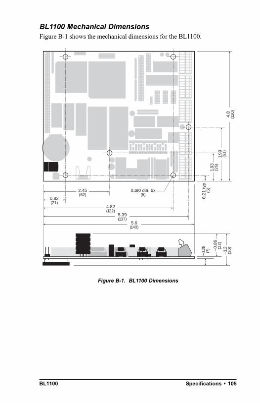
BL1100 Specifications s 105
BL1100 Mechanical DimensionsFigure B-1 shows the mechanical dimensions for the BL1100.
Figure B-1. BL1100 Dimensions
~0.2
8(7
)
1.99
(51)
1.03
(26)
0.21
typ
(5)0.190 dia, 6x
(5)2.45(62)
0.82(21)
5.39(137)
5.6(140)
~1.
2(3
0)~0.
86(2
2)
4.8
(120
)
4.82(122)
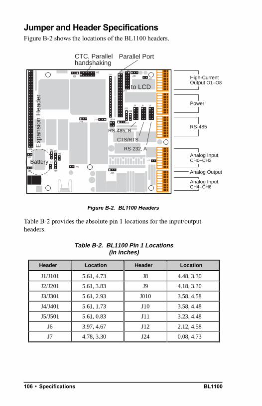
BL1100106 s Specifications
Jumper and Header SpecificationsFigure B-2 shows the locations of the BL1100 headers.
Figure B-2. BL1100 Headers
Table B-2 provides the absolute pin 1 locations for the input/outputheaders.
Table B-2. BL1100 Pin 1 Locations(in inches)
Header Location Header Location
J1/J101 5.61, 4.73 J8 4.48, 3.30
J2/J201 5.61, 3.83 J9 4.18, 3.30
J3/J301 5.61, 2.93 J010 3.58, 4.58
J4/J401 5.61, 1.73 J10 3.58, 4.48
J5/J501 5.61, 0.83 J11 3.23, 4.48
J6 3.97, 4.67 J12 2.12, 4.58
J7 4.78, 3.30 J24 0.08, 4.73
CTC, Parallelhandshaking
Parallel Port
to LCD
Exp
ansi
on H
eade
r
RS-485, B
RS-232, A
RS-485
CTS/RTS
Battery
J12
J10
J6
J31
J8 J7J9
J14
J13J18
J014
J17
J15J16
J19
J28
J22
J21
J24
J25
J010J11
J20
J27
J29
J32
J26 High-CurrentOutput O1–O8
Power
Analog Input,CH0–CH3
Analog Input,CH4–CH6
Analog Output
J30

BL1100 Specifications s 107
Table B-3 describes all the headers on the BL1100.
Wago Connector SignalsFigure B-3 shows the pinouts for Wago connectors J1/J101J5/J501.
Figure B-3. Pinouts for Wago Connectors
Table B-3. BL1100 Headers
Header Description
J1/J101 High-current outputs
J2/J201 Power
J3/J301 RS-485 (Z180 Port 1 or SIO Port A)
J4/J401 Analog inputs
J5/J501 Analog inputs and optional analog output
J6 LCD interface
J7 Z180 Port 0 (RS-232)
J8 SIO Port A or Z180 Port 1 (CTS/RTS)
J9 SIO Port B (RS-485)
J10/J010 KIO parallel port
J11 Alternate parallel port for user-installed flexiblekeypad connector
J12 Counter/timer circuit interface
J24 BL1100 expansion bus
1
OU
T8
OU
T7
OU
T6
OU
T5
OU
T4
OU
T3
OU
T2
OU
T1
J1/J101
GN
D+9
VIN
(+9
V)
GN
DR
EF
+ (+
2.5
V)
VC
C (
+5 V
)G
ND
SU
BK
J2/J201
/TX
CD
TX
CD
/TX
DD
TX
DD
/RX
CD
RX
CD
/RX
DD
RX
DD
J3/J301
CH
3HC
H3L
CH
2HC
H2L
CH
1HC
H1L
CH
0HC
H0L
J4/J401
CH
6HC
H6L
CH
5HC
H5L
CH
4HC
H4L
GN
DA
0/G
J5/J501
NOTES
1. J2/J201 SUB negative current supply for high-current driver, tied to ground unless split supply used. Must not float with respect to J2/J201J3/J301.2. J2/J201 VCC can be an input if the onboard supply is disabled (header J19).3. J2/J201 +9VIN is alternative input to power plug connector (J23).4. J5/J501 A0/G is analog ground or optional DAC output (selected on header J28).5. Do not mix analog grounds (J5/J501) with digital grounds (J2/J201).
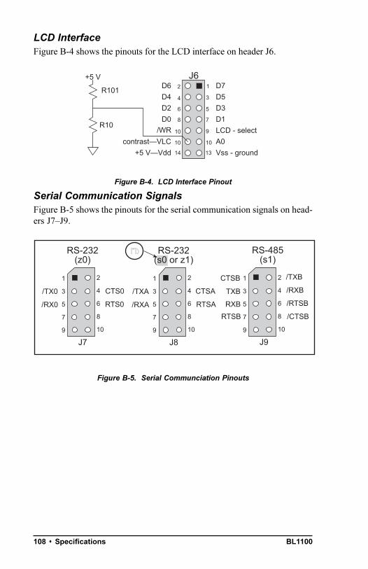
BL1100108 s Specifications
LCD InterfaceFigure B-4 shows the pinouts for the LCD interface on header J6.
Figure B-4. LCD Interface Pinout
Serial Communication SignalsFigure B-5 shows the pinouts for the serial communication signals on head-ers J7J9.
Figure B-5. Serial Communciation Pinouts
J7
/RX0
/TX0 CTS0
1
3
5
7
9
2
4
6
8
10
RTS0
RS-232(z0)
J8
/RXA
/TXA CTSA
1
3
5
7
9
2
4
6
8
10
RTSA
RS-232(s0 or z1)
J9
TXB
CTSB /TXB1
3
5
7
9
2
4
6
8
10
/RXB
RS-485(s1)
/RTSB
/CTSBRTSB
RXB
FD
contrastVLC+5 VVdd
R101
R10
12
1314
D7D5D3D1LCD - selectA0Vss - ground
D6D4D2D0
4 3
6 5
8 7
9
10 10
10/WR
J6+5 V
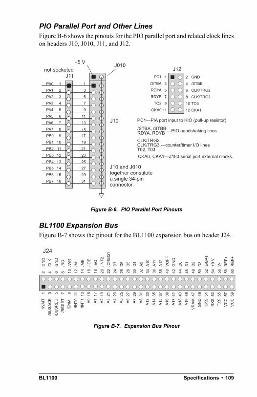
BL1100 Specifications s 109
1
2
PA0
PA1
PA2
PA3
PA4
PA5
PA6
PA7
PB0
PB1
PB2
PB3
PB4
PB5
PB6
PB7
3
4
5
8
9
10
11
12
13
14
15
16
7
6
J010
J10
1
3
5
7
9
1517
19
21
23
25
27
29
31
13
11
J10 and J010together constitutea single 34-pinconnector.
not socketedJ11
+5 VJ12
1
3
5
7
9
11
PC1
/STBA
RDYA
RDYB
TO2
CKA0
2
4
6
8
10
12
GND
/STBB
CLK/TRG2
CLK/TRG3
TO3
CKA1
PC1PIA port input to KIO (pull-up resistor)
/STBA, /STBBRDYA, RDYB PIO handshaking lines
CLK/TRG2,CLK/TRG3,counter/timer I/O linesT02, T03
CKA0, CKA1Z180 serial port external clocks.
PIO Parallel Port and Other LinesFigure B-6 shows the pinouts for the PIO parallel port and related clock lineson headers J10, J010, J11, and J12.
Figure B-6. PIO Parallel Port Pinouts
BL1100 Expansion BusFigure B-7 shows the pinout for the BL1100 expansion bus on header J24.
Figure B-7. Expansion Bus Pinout
1 3 5 7 9 11 13 15 17 19 21 23 25 27 29 31 33 35 37 39 41 43 45 47 49 51 53 55 57 59
/WA
IT
/BU
SA
CK
/BU
SR
EQ
/RE
SE
T
/EN
MI
/INT
0
/INT
1
A0
A1
A2
A3
A4
A5
A6
A7
A8
A13
A14
A15
A16
A17
A18
A19
VR
AM
GN
D
CK
S
RX
S
TX
S
VC
C
VC
C
2 4 6 8 10 12 14 16 18 20 22 24 26 28 30 32 34 36 38 40 42 44 46 48 50 52 54 56 58 60
GN
D
CLK
GN
D
/RD
/WR
/M1
/ME
/IOE
IEO
/INT
2
/DR
EQ
1
D7
D6
D5
D4
A9
A10
A11
A12
VO
FF
GN
D
D0
D1
D2
D3
E/B
AT
+9 V
V-
RE
F+
RE
F+
J24

BL1100110 s Specifications
Jumper ConfigurationsTable B-4 lists the jumper settings for the applicable BL1100 headers.
Table B-4. Standard BL1100 Jumper Settings
Header Pins DescriptionFactoryDefault
1–2Connect for factory-default RS-232 or RS-485programming mode, remove for run mode oruser-defined programming mode
Connected
6–10 CTC3 output drives CTC2
8–9 CTC2 output drives CTC3
6–11 CTC2 operates at 16X baud rate of z0
6–12 CTC2 operates at 16X baud rate of z1
8–11 CTC3 operates at 16X baud rate of z0
8–12 CTC3 operates at 16X baud rate of z1
9–11CTC2 drives external clock at 1/16 z0 baudrate
J12
10–12CTC3 drives external clock at 1/16 z1 baudrate
1–2 SIO Port A to RS-232 (J8) Connected
2–3 SIO Port A to RS-485 (J3)J13
3–4 ZIO Port 1 to RS-485 (J3) Connected
1–4 ZIO Port 1 to RS-232 (J8)
1–2 SIO Port A to RS-485 (J3)J14
2–3 ZIO Port 1 to RS-485 (J3) Connected
1–2 RX and TX clocks come from SIO Connected
J0142–4
TX clock from SIO, RX clock from externalsource via pins 3–4 of header J3/J301
1–2 SRAM smaller than 256K ConnectedJ15
2–3 SRAM 256K or larger
1–2 EPROM 32 K ConnectedJ16
2–4 EPROM larger than 32K
J17 1–2Connect to enable excitation resistors foranalog input signal conditioning op-amps
Notconnected
continued…

BL1100 Specifications s 111
Table B-4. Standard BL1100 Jumper Settings (concluded)
Header Pins Description FactoryDefault
1–2 RS-485 three-state always enabled Connected
2–3 RS-485 three-state controlled by PB0J18
none RS-485 three-state always disabled
J19 1–2Connect to enable onboard +5 V powersupply, disconnect for external power supply
Connected
1–2 EPROM smaller than 256K ConnectedJ20
2–4 EPROM 256K
1–2 Write-protect upper part of EEPROM ConnectedJ21
2–3 Write-enable upper part of EEPROM
J22 1–2 Connect to enable watchdog timerNot
connected
J25 1–2Startup mode factory-default RS-232 or readfrom EEPROM
Connected
1–2 Remote reset using RXC
2–3 Remote reset using CTSBJ26
none No remote reset
Notinstalled
J27 1–2Connect to enable switching power supply,disconnect for time/date clock to controlpower supply
Connected
1–2 Output DAC to pin 1 on J5/J501J28
2–3 Pin 1 of J5/J501 is analog ground Connected
1–2 Connects E to expansion bus J24 pin 52
J292–3
Connects BATACT to expansion bus J24 pin52
Notinstalled
J31 1–2Ties high-voltage driver SUB signal to groundto keep it from floating
Connected
J32 1–2Connect to control use of ENMI signal onexpansion bus J24 pin 9
Connected

BL1100112 s Specifications
BL1100 Memory, I/O Map and Interrupt Vectors 113
APPENDIX C: MEMORY, I/O MAP, ANDINTERRUPT VECTORS
Appendix C provides detailed information on memory, provides an I/Omap, and lists the interrupt vectors.
BL1100114 s Memory, I/O Map and Interrupt Vectors
BL1100 MemoryThere are two 32-pin memory sockets, one for ROM and one for RAM.Sockets U011 and U10 will accept either 32-pin or 28-pin memory chips.
Physical MemoryDepending on PAL coding and wiring, the BL1100 can address 256K or512K of ROM, and 512K of RAM. Figure C-1 illustrates the physicalmemory mapping.
Figure C-1. BL1100 Physical Memory Map
The memory chips usually installed on the BL1100 have a capacity lessthan 512K. Typical SRAM chips have 32K or 128K.
If there is less than 512K of SRAM, addresses outside thememory range will map to addresses within the range. Forexample, addresses on a 32K chip evaluate modulo 32K.Therefore, data may seem to be replicated in memory. Orworse, you data may be overwritten.
Memory ManagementZ180 instructions can specify 16-bit addresses, giving a logical addressspace of 64K (65,536 bytes). Dynamic C supports a 1M physical addressspace (20-bit addresses).
An on-chip memory management unit (MMU) translates 16-bit Z180addresses to 20-bit memory addresses. Three MMU registers (CBAR,CBR, and BBR) divide the logical space into three sections and map eachsection onto physical memory, as shown in Figure C-2. (Potentially, thethree sections may overlap or be of zero size.)
FFFFF
80000
00000
FFFFF
00000
C0000
40000
(UNMAPPED)512KSRAM
512KEPROM
512KSRAM
256KEPROM
!
BL1100 Memory, I/O Map and Interrupt Vectors s 115
Figure C-2. Mapping Logical Memory to Physical Memory
The logical address space is partitioned on 4K boundaries. Given a 16-bitaddress, the Z180 uses CBAR to determine whether the address is incommon area 1, common area 0, or the bank area. If the address is incommon area 1, the Z180 uses the CBR as the base to calculate thephysical address. If the address is in the bank area, the Z180 uses theBBR. If the address is in common area 0, the Z180 uses a base of 00H.
The physical address is, essentially,
(base << 12) + logical address,
as shown in Figure C-3.
Figure C-3. Determining Physical Address from Logical Address
Logical Space Physical Space
FFFF
0000
COMMONAREA 1
BANKAREA
COMMONAREA 0
CBARCom Bank
00000
FFFFF
CBR
BBR
CBAR
CBR
BBR
Common/Bank Area Register
Common Base Register
Bank Base Register
logical address
15 12 11 0
+base
physical address
19 0
BL1100116 s Memory, I/O Map and Interrupt Vectors
How Dynamic C Uses the MMUIn order to use a 1M physical address space, Dynamic C partitions logicalspace into three areas, which correspond to the Z180 common and bankareas listed in Table C-1.
The XMEM area has many mappings to physical memory. The root andBIOS have 1:1 mappings.
Dynamic C can either compile to RAM (for development) or compileto ROM (for a standalone programs), as shown in Figure C-4.
See the Dynamic C Technical Reference manual for details.
Dynamic C uses physical memory in slightly different ways, depending onthe options selected by the programmer. When compiling to ROM, thecompiler places root code (including constants and preset variables) inROM, directly above the BIOS. When compiling to RAM, the entire root(code and data) is placed in RAM.
Z180 memory management is not automatic. The Dynamic C compileremits code that will set the mapping registers. Assembly language pro-grammers must do it themselves. However, Dynamic C does generatebouncers for assembly language calls to XMEM functions. Dynamic C
Table C-1. Dynamic C Logical Space Partitions
Name Size Description
BIOS 8K Basic Input/Output System. Loosely named, the BIOSis always present and is always mapped to address 0 ofROM. The BIOS contains the power-up code, thecommunication kernel, and important system features.The BIOS corresponds to common area 0.
ROOT 48K The area between the BIOS and XMEM (the bankarea). The root—normal memory—resides in a fixedportion of physical memory. Root code grows upwardin logical space from address 2000 (hex) and root data(static variables, stack and heap) grow down fromE000. (Initialized static variables are placed withcode, in ROM or RAM.)
XMEM 8K Extended Memory. XMEM is essentially an 8 kbyte“window” into physical memory. XMEM can map toany part of physical memory (ROM or RAM) simplyby changing the CBR. XMEM corresponds tocommon area 1.
$
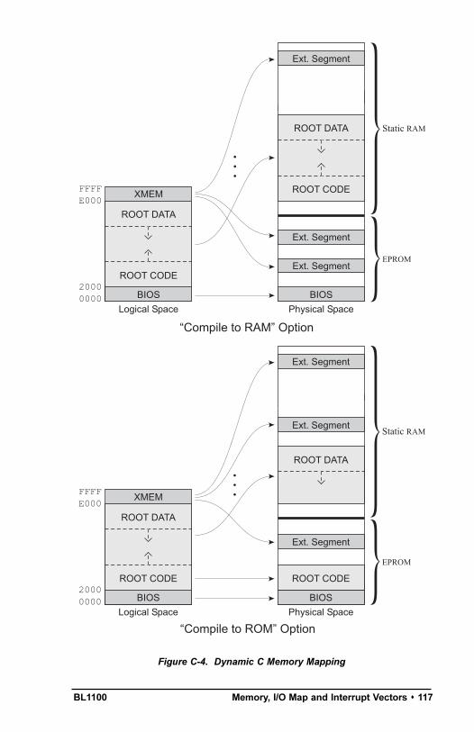
BL1100 Memory, I/O Map and Interrupt Vectors s 117
Logical Space Physical Space
FFFFE000
20000000
XMEM
ROOT DATA
Static RAM
EPROM
ROOT CODE
BIOS
ROOT DATA
ROOT CODE
BIOS
Ext. Segment
Ext. Segment
Ext. Segment
Compile to RAM Option
Logical Space Physical Space
FFFFE000
20000000
XMEM
ROOT DATA
Static RAM
EPROM
ROOT CODE
BIOS
BIOS
Ext. Segment
Ext. Segment
Ext. Segment
ROOT CODE
ROOT DATA
Compile to ROM Option
Figure C-4. Dynamic C Memory Mapping

BL1100118 s Memory, I/O Map and Interrupt Vectors
supports the use of extended memory with several extensions to the Clanguage: function classes, additional compiler directives, and extendedmemory data declarations.
Control over Memory MappingThe programmer has complete control over how Dynamic C allocates andmaps memory with the options on the SETUP menu listed in Table C-2.
See the Dynamic C Technical Reference manual for details.
Extended Memory CodePhysical memory is divided into 4K pages. Two of these pages arevisible in the extended memory window (XMEM) at any one time.Additional code is required to handling calls to other functions or jumps tolocations not currently mapped in the extended memory window.
A program can use many 4K pages of extended memory. Normally, thepage being executed is mapped to the address region E000H to F000H. Asthe execution approaches F000, the pages are shifted so that the code inthe region F000 to FFFF is moved down to the E000 to F000 region. Abouncer in low memory is called to accomplish this task. The bouncermodifies the memory management unit (MMU) to slide the code down onepage and then jumps to the new location. This transfer of control is madeis at the end of the first statement that crosses F000. No single C expres-sion can be more than 4K long.
However, statements such as switch or while that cause program jumpscan be as long as desired. A bouncer is used to execute the jump if a jumpcrosses page boundaries.
Table C-2. Dynamic C Memory Mapping Options
Option Description
ReserveControl
Specifies the size of the root memory reserve or theextended memory reserve.
RAM MapControl
Specifies how RAM is to be mapped when “compiling toRAM.”
ROM MapControl
Specifies how ROM is to be mapped when “compiling toROM.”
$

BL1100 Memory, I/O Map and Interrupt Vectors s 119
Any C function can call any other C function, no matter where in memoryit is located. However, it is less efficient to call a function located inextended memory than to call a function located in root memory, because abouncer must be used to modify the memory management registers beforeand after the call. A separate bouncer is compiled for each call and isspecific to that particular call. The compiler places all bouncers in rootmemory.
Programs run faster when functions that are short and frequently used areplaced in the root memory.
Extended Memory DataAccessing data in extended memory is not as transparent as callingfunctions in extended memory.
Dynamic C has two keywords, xdata and xstring, and some libraryfunctions that allow data to be stored in extended memory.
The deluxe version of Dynamic C is required to be able todeclare extended memory data.
Library functions (xmem2root, root2xmem, xstrlen, xgetlong) existfor manipulating extended memory data.
See the Dynamic C manuals for details.
Execution TimingTable C-3 provides the execution times for a BL1100 with a 9.216 MHzclock and a 12.288 MHz clock. These times reflect the use of Dynamic Clibraries. The time required to read from memory is included, but the timeto store a result is not.
The Z180 memory cycle requires faster memory during certain op-codefetch cycles (LIR cycles). The term 1/2 wait state means that thesecycles are stretched by adding a wait state. The term 0 wait state meansthat none of the cycles have wait states added. Generally, 1/2 wait statecycles are used for higher clock speeds. Zero wait states are fine forslower clock speeds.
!
$
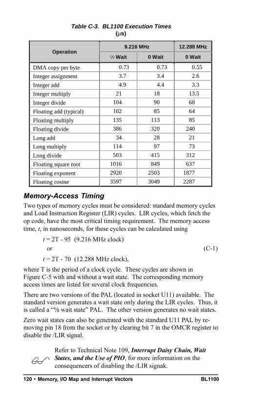
BL1100120 s Memory, I/O Map and Interrupt Vectors
Table C-3. BL1100 Execution Times(µs)
9.216 MHz 12.288 MHzOperation
2 Wait 0 Wait 0 Wait
DMA copy per byte 0.73 0.73 0.55
Integer assignment 3.7 3.4 2.6
Integer add 4.9 4.4 3.3
Integer multiply 21 18 13.5
Integer divide 104 90 68
Floating add (typical) 102 85 64
Floating multiply 135 113 85
Floating divide 386 320 240
Long add 34 28 21
Long multiply 114 97 73
Long divide 503 415 312
Floating square root 1016 849 637
Floating exponent 2920 2503 1877
Floating cosine 3597 3049 2287
Memory-Access TimingTwo types of memory cycles must be considered: standard memory cyclesand Load Instruction Register (LIR) cycles. LIR cycles, which fetch theop code, have the most critical timing requirement. The memory accesstime, t, in nanoseconds, for these cycles can be calculated using
t = 2T - 95 (9.216 MHz clock)or (C-1)
t = 2T - 70 (12.288 MHz clock),
where T is the period of a clock cycle. These cycles are shown inFigure C-5 with and without a wait state. The corresponding memoryaccess times are listed for several clock frequencies.
There are two versions of the PAL (located in socket U11) available. Thestandard version generates a wait state only during the LIR cycles. Thus, itis called a 2 wait state PAL. The other version generates no wait states.
Zero wait states can also be generated with the standard U11 PAL by re-moving pin 18 from the socket or by clearing bit 7 in the OMCR register todisable the /LIR signal.
Refer to Technical Note 109, Interrupt Daisy Chain, WaitStates, and the Use of PIO, for more information on theconsequencers of disabling the /LIR signak.
$

BL1100 Memory, I/O Map and Interrupt Vectors s 121
T1 T2 TwT3
address
T1 T2 T3
address
data data
TAD = 70 ns TAD = 70 nsTDRS = 25 ns TDRS = 25 ns
0 wait states 1 wait state
Figure C-5. Memory Cycles for 9.216 MHz ProcessorWith and Without a Wait State
12.288 MHz0 wait access time = 2T - 70 ns 1 wait access time = 3T - 70 ns= 93 ns for 12.288 MHz clock = 162 ns for 12.288 MHz clock
9.216 MHz0 wait access time = 2T - 95 ns 1 wait access time = 3T - 95 ns= 105 ns for 10.00 MHz clock = 205 ns for 10.00 MHz clock= 122 ns for 9.216 MHz clock = 230 ns for 9.216 MHz clock= 229 MHz for 6.144 MHz clock = 391 ns for 6.144 MHz clock
Table C-4 lists the memory access times required for various clockfrequencies and wait states.
The times for the 12.288 MHz clock are based on a faster version of theZ180, which is why the access time can be slower. However, the SRAMsaccess time must equal that of the EPROM during program developmentor when executing code in SRAM, because code executes from SRAMduring these periods.
Table C-4. Memory Access Times(ns)
Clock Frequency EPROM SRAM
9.216 MHz 2 wait state 176 176
9.216 MHz 0 wait states 122 176
12.288 MHz 2 wait state 133 133
12.288 MHz 0 wait states 93 133
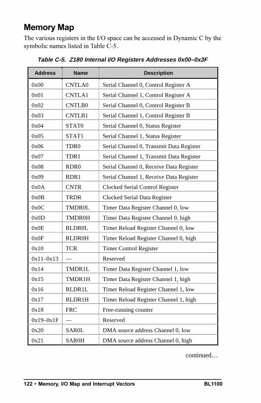
BL1100122 s Memory, I/O Map and Interrupt Vectors
Table C-5. Z180 Internal I/O Registers Addresses 0x00–0x3F
Address Name Description
0x00 CNTLA0 Serial Channel 0, Control Register A
0x01 CNTLA1 Serial Channel 1, Control Register A
0x02 CNTLB0 Serial Channel 0, Control Register B
0x03 CNTLB1 Serial Channel 1, Control Register B
0x04 STAT0 Serial Channel 0, Status Register
0x05 STAT1 Serial Channel 1, Status Register
0x06 TDR0 Serial Channel 0, Transmit Data Register
0x07 TDR1 Serial Channel 1, Transmit Data Register
0x08 RDR0 Serial Channel 0, Receive Data Register
0x09 RDR1 Serial Channel 1, Receive Data Register
0x0A CNTR Clocked Serial Control Register
0x0B TRDR Clocked Serial Data Register
0x0C TMDR0L Timer Data Register Channel 0, low
0x0D TMDR0H Timer Data Register Channel 0, high
0x0E RLDR0L Timer Reload Register Channel 0, low
0x0F RLDR0H Timer Reload Register Channel 0, high
0x10 TCR Timer Control Register
0x11–0x13 — Reserved
0x14 TMDR1L Timer Data Register Channel 1, low
0x15 TMDR1H Timer Data Register Channel 1, high
0x16 RLDR1L Timer Reload Register Channel 1, low
0x17 RLDR1H Timer Reload Register Channel 1, high
0x18 FRC Free-running counter
0x19–0x1F — Reserved
0x20 SAR0L DMA source address Channel 0, low
0x21 SAR0H DMA source address Channel 0, high
continued…
Memory MapThe various registers in the I/O space can be accessed in Dynamic C by thesymbolic names listed in Table C-5.
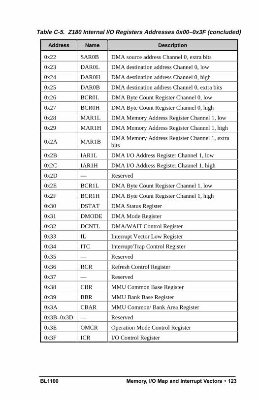
BL1100 Memory, I/O Map and Interrupt Vectors s 123
Table C-5. Z180 Internal I/O Registers Addresses 0x00–0x3F (concluded )
Address Name Description
0x22 SAR0B DMA source address Channel 0, extra bits
0x23 DAR0L DMA destination address Channel 0, low
0x24 DAR0H DMA destination address Channel 0, high
0x25 DAR0B DMA destination address Channel 0, extra bits
0x26 BCR0L DMA Byte Count Register Channel 0, low
0x27 BCR0H DMA Byte Count Register Channel 0, high
0x28 MAR1L DMA Memory Address Register Channel 1, low
0x29 MAR1H DMA Memory Address Register Channel 1, high
0x2A MAR1BDMA Memory Address Register Channel 1, extrabits
0x2B IAR1L DMA I/O Address Register Channel 1, low
0x2C IAR1H DMA I/O Address Register Channel 1, high
0x2D — Reserved
0x2E BCR1L DMA Byte Count Register Channel 1, low
0x2F BCR1H DMA Byte Count Register Channel 1, high
0x30 DSTAT DMA Status Register
0x31 DMODE DMA Mode Register
0x32 DCNTL DMA/WAIT Control Register
0x33 IL Interrupt Vector Low Register
0x34 ITC Interrupt/Trap Control Register
0x35 — Reserved
0x36 RCR Refresh Control Register
0x37 — Reserved
0x38 CBR MMU Common Base Register
0x39 BBR MMU Bank Base Register
0x3A CBAR MMU Common/ Bank Area Register
0x3B–0x3D — Reserved
0x3E OMCR Operation Mode Control Register
0x3F ICR I/O Control Register
BL1100124 s Memory, I/O Map and Interrupt Vectors
These names are treated as unsigned integer constants. Use the libraryfunctions inport and outport to access the I/O registers.
data_value = inport( CNTLA0 );
outport( CNTLA0, data_value );
The library functions IBIT, ISET, and IRES can be used to set and clearbits in I/O registers.
The internal registers for the I/O devices built into to the Z180 processoroccupy the first 40 (hex) addresses of the I/O space.
The addresses in Table C-6 cover the KIO registers.
Table C-6. KIO Registers Addresses 40-4F
Address Name Description
40 PIODA PIO Port A Data
41 PIOCA PIO Port A Control
42 PIODB PIO Port B Data
43 PIOCB PIO Port B Control
44 CTC0 CTC Channel 0
45 CTC1 CTC Channel 1
46 CTC2 CTC Channel 2
47 CTC3 CTC Channel 3
48 SIODA SIO Channel A Data
49 SIOCA SIO Channel A Control
4A SIODB SIO Channel B Data
4B SIOCB SIO Channel B Control
4C PIAD PIA Port C Data
4D PIAC PIA port C Control
4E KIOC KIO Control
4F — Reserved
BL1100 Memory, I/O Map and Interrupt Vectors s 125
Table C-7 lists the addresses of other BL1000 registers.
Table C-7. Other Register Addresses (60–FF)
Address Name Description
60 SDA_R Read only, 1 bit, EEPROM SDA register
62 LCD LCD interface R/W
64 BMS Strobe serial register to output register 5841
66 ENB485 Enable 485 driver, write only, 1 bit
68 BMO Write only enable 5841 output 1 bit
6A AD_ADE Write only, 1 bit register, enable A/D
6C SC Write only, 1 bit register, EEPROM clock
6E SDA_W Write only, 1 bit register, EEPROM data
70–7F — Reserved for duplicate decodes
80–FF — Unused I/O space
BL1100126 s Memory, I/O Map and Interrupt Vectors
Table C-8. Epson 72421 Real-Time Clock Registers
Address Bit 3 Bit 2 Bit1 Bit 0 Description
50 S8 S4 S2 S1 seconds, units
51 S40 S20 S10 seconds, tens
52 M8 M4 M2 M1 minutes, units
53 M40 M20 M10 minutes, tens
54 H8 H4 H2 H1 hours, units
55 AM/PM H20 H10 hours, tens
56 D8 D4 D2 D1 days, units
57 D20 D10 days, tens
58 M8 M4 M2 M1 months, units
59 M10 months, tens
5A Y8 Y4 Y2 Y1 years, units
5B Y80 Y40 Y20 Y10 years, tens
5C W4 W2 W1 weeks
5D30ADJ
IRQFLG
BUSY HOLD Register D
5E T1 T0INTR/STND
MASK Register E
5F TEST 12/24 STOP RSET Register F
Time/Date ClockThe battery-backed clock appears as 16 I/O registers with addresses of 505F. The 16 registers are 4 bits wide. The upper 4 bits of the register areundefined. The register arrangement is shown in Table C-8.
The 4-bit registers are mostly binary-coded decimal numbersthat make up the date and time.
The following notes apply to the registers listed in Table C-8.
Set the 12/24 bit to 1 for 24-hour mode and 0 for 12-hour mode. Thea.m./p.m. bit will be 1 for p.m. Mask out the a.m./p.m. bit in the24-hour mode.
The days of the week are represented by 0 for Sunday and 6 for Saturday.
Leap year is automatically taken into account.
Set the year to 90 for 1990, to 91 for 1991, and so on.
Constant reading of the clock (as in a tight loop) will create a loss ofaccuracy.
!

BL1100 Memory, I/O Map and Interrupt Vectors s 127
Table C-10. Interrupt Vectors for Z180 Internal Devices
Address Name Description
0x00 INT1_VEC Expansion bus attention INT1 vector
0x02 INT2_VEC INT2 vector
0x04 PRT0_VEC PRT Timer Channel 0
0x06 PRT1_VEC PRT Timer Channel 1
0x08 DMA0_VEC DMA Channel 0
0x0A DMA1_VEC DMA Channel 1
0x0C CSIO_VEC Clocked Serial I/O
0x0E SER0_VEC Asynchronous Serial Port Channel 0
0x10 SER1_VEC Asynchronous Serial Port Channel 1
Initialized Memory LocationsTable C-9 lists the constants that are initialized at startup.
To access these variables, declare them as follows.
extern unsigned int CLOCKSPEED
extern unsigned int BAUDCODE
extern unsigned int JUMPERS
Interrupt VectorsTables C-10, C-11, and C-12 present a suggested interrupt vector map.Most of these interrupt vectors can be altered under software control. Theaddresses are given in hex, relative to the start of the interrupt vector page,as determined by the contents of the I-register. These are the defaultinterrupt vectors set by the boot code in the Dynamic C EPROM.
Table C-9. Constants Initialized at Setup
CLOCKSPEED Integer containing the clock speed read in multiples of1200 Hz from the EEPROM at startup
BAUDCODE Integer containing the baud rate in multiples of1200 bps as read from the EEPROM at startup
JUMPERS Byte read from the P1B port of the KIO at startup
BL1100128 s Memory, I/O Map and Interrupt Vectors
A directive such as the following is used to vector an interrupt to a userfunction in Dynamic C.
#INT_VEC 0x10 myfunction
This statement causes the interrupt at offset 10H (Serial Port 1 of theZ180) to invoke the function myfunction(). The function must bedeclared with the interrupt keyword as follows.
interrupt myfunction() ...
Table C-11. Interrupt Vectors for KIO Devices
Address Name Description
0x12 PIOA_VEC PIO parallel port Channel A
0x14 PIOB_VEC PIO parallel port Channel B
0x18 CTC0_VEC CTC Timer Channel 0
0x1A CTC1_VEC CTC Timer Channel 1
0x1C CTC2_VEC CTC Timer Channel 2
0x1E CTC3_VEC CTC Timer Channel 3
Table C-12. SIO Interrupt Vectors
Address Name Description
0x20 SIOBT_VEC Channel B Transmit Buffer Empty
0x22 SIOBEX_VEC Channel B External/Status Change
0x24 SIOBR_VEC Channel B Receive Character Ready
0x26 SIOBER_VEC Channel B Special Receive Condition
0x28 SIOAT_VEC Channel A Transmit Buffer Empty
0x2A SIOAEX_VEC Channel A External/Status Change
0x2C SIOAR_VEC Channel A Receive Character Ready
0x2E SIOAER_VEC Channel A Special Receive Condition

BL1100 Memory, I/O Map and Interrupt Vectors s 129
Nonmaskable InterruptsPower-Fail InterruptsThe following sequence of events takes place when power fails.
1. The nonmaskable interrupt (NMI) signaling power failure is triggeredwhenever the unregulated DC input voltage falls below approximately8 V (subject to voltage divider R3/R4).
2. The system reset is triggered when the regulated +5 V falls below4.5 V; the reset remains enabled as the voltage falls further. At thispoint, the chip select for the SRAM is forced high (standby mode).Power for the time/date clock and the SRAM is switched to the lithiumbackup battery as the regulated voltage falls below the battery voltage(approximately 3 V).
The following sample routine demonstrates how to handle a power-failinterrupt.
#JUMP_VEC NMI_INT myint
interrupt retn myint()body of interrupt routine...while( 1 ) if( !powerlo() ) return;
Normally, a power-fail interrupt routine will not return. Instead, it willexecute shutdown code and then enter a loop until the +5 V falls lowenough to trigger a reset. However, the voltage might fall low enough in abrownout situation to trigger the power-fail interrupt but not the reset,resulting in an endless hangup. The library function powerlo returns 1 ifthe voltage level is below the NMI threshold; otherwise, it returns 0. Callpowerlo only from an NMI routine. If powerlo detects that the low-voltage condition has reversed itself, then the power-failure routine canrestart execution. If a low-voltage condition that is not fatally low persists,then the user must decide decide what action to take, if any.
A situation similar to brownout occurs if the power supply is overloaded.Say the load temporarily increases, perhaps when an LED is turned on,causing the power supply to appear to have failed. The interrupt routinesheds some of the load by doing a shutdown procedure, causing the power-fail condition to go away. If no action is taken to correct the overload, thesystem will oscillate around the power fail. To correct this, use a largerpower supply.
Do not forget the interaction that can occur between the watchdog timerand the power-fail interrupt. If the watchdog timer is enabled and abrownout causes an extended stay in the power-fail interrupt routine, thenthe watchdog can time out, causing a system restart.

BL1100130 s Memory, I/O Map and Interrupt Vectors
Even if the power is cut off from the board abruptly, a certain amount ofcomputing time will remain before the +5 V supply falls below 4.5 V. Theamount of time depends on the size of the capacitors in the power supply.The standard wall transformer provides about 10 ms. If the power cable isabruptly removed from the BL1100, then only the capacitors on the boardare available and the time is reduced to a few hundred microseconds.These times can vary considerably, depending on the board configurationand the other loads, if any, drawing from the boards power supply.
The time interval between detection of a power failure and entry to theusers power-fail interrupt routine is approximately 100 µs, or less ifDynamic Cs nonmaskable interrupt communications are not in use.
It is hard to test power-fail interrupt routines presents because the inter-rupts are normally disabled. Probably the best test method involvesleaving messages in battery-backed memory to track the execution of thepower-fail routines. If a variable transformer is available to drive the walltransformer, then brownouts and other types of power-fail conditions canbe easily simulated.
The power-failure interrupt must be disabled if an external+5 V power supply is used.
Jump VectorsJump vectors are special interrupts that are different from INT0 interrupts.Instead of loading the address of the interrupt routine from the interruptvector, jump vectors cause a jump directly to the address of the vector, forexample,
0x66 nonmaskable power-failure interrupt,
that contains a jump instruction to the interrupt routine.
Since nonmaskable interrupts can be used for Dynamic C communications,the interrupt vector for power failure is normally stored just in front of theDynamic C program. A vector may be stored there by the followingcommand.
#JUMP_VEC NMI_VEC name
The Dynamic C communication routines relay to this vector when thenonmaskable interrupt is caused by a power failure rather than by a serialinterrupt.
!
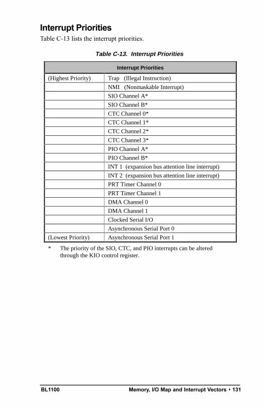
BL1100 Memory, I/O Map and Interrupt Vectors s 131
Table C-13. Interrupt Priorities
Interrupt Priorities
(Highest Priority) Trap (Illegal Instruction)
NMI (Nonmaskable Interrupt)
SIO Channel A*
SIO Channel B*
CTC Channel 0*
CTC Channel 1*
CTC Channel 2*
CTC Channel 3*
PIO Channel A*
PIO Channel B*
INT 1 (expansion bus attention line interrupt)
INT 2 (expansion bus attention line interrupt)
PRT Timer Channel 0
PRT Timer Channel 1
DMA Channel 0
DMA Channel 1
Clocked Serial I/O
Asynchronous Serial Port 0
(Lowest Priority) Asynchronous Serial Port 1
* The priority of the SIO, CTC, and PIO interrupts can be alteredthrough the KIO control register.
Interrupt PrioritiesTable C-13 lists the interrupt priorities.

BL1100132 s Memory, I/O Map and Interrupt Vectors

BL1100 EEPROM 133
APPENDIX D: EEPROM

BL1100134 s EEPROM
ParametersThe onboard EEPROM (electrically erasable, programmable, read-onlymemory) is used to store the constants and parameters listed in Table D-1.
The EEPROM has 512 bytes. Bytes 0255 can be written to at any time,but the upper 256 bytes can be written to only when header J21 is enabled(pins 2 and 3 are connected). Connect pins 1 and 2 on J21 to write-protectthe EEPROM.
Figure D-1 shows the EEPROM memory and J21 jumper settings.
Figure D-1. BL1100 EEPROM and Jumper Settings
Table D-1. BL1100 EEPROM Assignments
Address Bytes Function
00 1
Operating Mode:1—RS-232 programming via header J72—RS-485 programming with NMI via header
J94—RS-485 programming with regular interrupts
via header J98—Run user program in SRAM on startup
01 1 Baud rate code (in multiples of 1200 bps)
100 6 Unit serial number—binary-coded decimal timeand date in the format: seconds, minutes, hour,day, month, year
108 2 Clock speed (in multiples of 1200 Hz)
10A 1Wait states, value to be inserted in DCNTL forI/O and memory wait states. Default = 0x20 for3 I/O wait states and 0 memory wait states.
10C 2 Network node address
110 4 Reference temperature coefficient:T (K) = coefficient × ADC value
256 x 8
256 x 8protectable 1
2
3
00
100
200 J21
1
2
3
J21
EEPROMwrite-protected
EEPROMwrite-enabled

BL1100 EEPROM s 135
Library RoutinesThe following library routines can be used to read and write the EEPROM:
int ee_rd( int address );
int ee_wr( int address, byte data );
The function ee_rd returns a data value or, if a hardware failure occurred,1. The function ee_wr returns 1 if a hardware failure occurred, 2 if anattempt was made to write to the upper 256 bytes with the protectionjumper (J16) installed, or 0 to indicate a successful write. A write-protection violation does not wear out the EEPROM. These routines eachrequire about 2 ms to execute. They are not re-entrant, that is, only oneroutine at a time will run.
The EEPROM has a rated lifetime of only 10,000 writes(unlimited reads). Do not write the EEPROM from within aloop. The EEPROM should be written to only in response to ahuman request for each write.
!

BL1100136 s EEPROM

BL1100 Power Management 137
APPENDIX E: POWER MANAGEMENT
Appendix E provides information about power consumption and intermit-tent operation.
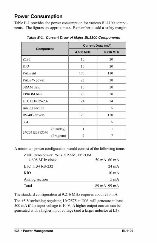
BL1100138 s Power Management
Power ConsumptionTable E-1 provides the power consumption for various BL1100 compo-nents. The figures are approximate. Remember to add a safety margin.
A minimum power configuration would consist of the following items.
Z180, zero-power PALs, SRAM, EPROM,4.608 MHz clock 50 mA60 mA
LTC 1134 RS-232 24 mA
KIO 10 mA
Analog section 5 mA
Total 89 mA99 mA
The standard configuration at 9.216 MHz requires about 270 mA.
The +5 V switching regulator, LM2575 at U06, will generate at least500 mA if the input voltage is 10 V. A higher output current can begenerated with a higher input voltage (and a larger inductor at L3).
Table E-1. Current Draw of Major BL1100 Components
Current Draw (mA)Component
4.608 MHz 9.216 MHz
Z180 10 20
KIO 10 20
PALs std 100 110
PALs 3 power 25 28
SRAM 32K 10 20
EPROM 64K 20 30
LTC1134 RS-232 24 24
Analog section 5 5
RS-485 drivers 120 120
5841 5 5
(Standby) 1 124C04 EEPROM
(Program) 7 7

BL1100 Power Management s 139
The LM340 linear regulator (U13) is rated for 1 A for an input voltage of10 V, and a maximum ambient temperature of 45°C. The LM340 canoperate at up to 85°C when producing up to 500 mA, which is a highertemperature rating than the rating for the rest of the components.
Intermittent OperationPower can be turned on and off under software control on BL1100sequipped with a switching power regulator. This is done under the controlof the time/date clock or by an external switch.
The switching power regulator turns off when the signal VOFF is raisedhigh and turns on when VOFF is pulled low. When the regulator turns on,there is a power-on reset lasting for approximately 50 ms. After the power-on reset, the programs main routine begins processing after approximately10 ms.
VOFF can be driven by an external circuit, permanently enabled (low) witha jumper by installing a jumper across J27, or controlled by the open drainoutput of the 72421 clock chip (jumper across header J27 removed). Thepower can be controlled in one of the following ways.
1. An operator pushbutton grounds VOFF, enabling power. The softwarethen calls the library function powerup to keep the power enabled afterthe operator releases the pushbutton. When power is no longer needed,the program calls the function powerdown to turn the power off untilanother external event re-enables power. This logic can be used tocreate a battery-powered instrument that turns off automatically after acertain period of inactivity to conserve the battery.
2. Power is turned on periodically for a short period of time. Theavailable periods are
1 second,1 minute, and1 hour.
Power is turned on at the start of the next period. If, for example, thewakeup time is set to one minute, the board will wake up when theminute changes, not after one minute has elapsed. If the program runsfor 10 s and then goes to sleep, 50 s will elapse before the board wakesup again.
The minimum time for power to be on is approximately 60 ms. Powerconsumption will be decreased by a factor of approximately 15 to 1 ifpower is on for only 60 ms in every second. If power is on only once aminute, the ratio will be 900 to 1. Once every hour reduces the ratioto54,000 to 1. If a 9 V, 500 mA·h battery is used, the battery life with

BL1100140 s Power Management
power on continuously is only 1.5 h. The battery life would be extended toapproximately one day with power enabled every second. Enablingpower only once a minute extends the battery life to approximately twomonths. Enabling power once every hour extends battery life toapproximately 10 years. This type of power usage is convenient fordata collection applications, for example, recording the temperature atone-minute intervals under battery power.
The following library functions support intermittent operation.
setperiodic( int code )
This function specifies the interval between VOFF pulses from thedate/time clock: code = 4 Þ 1 second, 8 Þ 1 minute, 12 Þ 1 hour.
sleep()
Turns power off until next periodic time.
The periodic interrupts depend on the modes set into the battery-backed memory of the date/time clock (the 72421 chip). If the 72421is upset by a voltage transient, or the lithium battery goes dead, theboard could fail to wake up at the specified time. Z-World recom-mends adding an external wakeup circuit to replace or supplement the72421 for critical applications that must run unattended.

BL1100 Opto 22 Support 141
APPENDIX F: OPTO 22 SUPPORT
Appendix F summarizes the BL1100’s Opto 22 support and compares theperformance of the BL1100 with Opto 22 controllers.
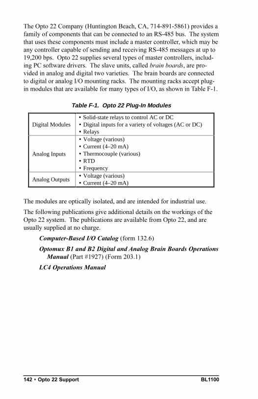
BL1100142 s Opto 22 Support
The Opto 22 Company (Huntington Beach, CA, 714-891-5861) provides afamily of components that can be connected to an RS-485 bus. The systemthat uses these components must include a master controller, which may beany controller capable of sending and receiving RS-485 messages at up to19,200 bps. Opto 22 supplies several types of master controllers, includ-ing PC software drivers. The slave units, called brain boards, are pro-vided in analog and digital two varieties. The brain boards are connectedto digital or analog I/O mounting racks. The mounting racks accept plug-in modules that are available for many types of I/O, as shown in Table F-1.
The modules are optically isolated, and are intended for industrial use.
The following publications give additional details on the workings of theOpto 22 system. The publications are available from Opto 22, and areusually supplied at no charge.
Computer-Based I/O Catalog (form 132.6)
Optomux B1 and B2 Digital and Analog Brain Boards OperationsManual (Part #1927) (Form 203.1)
LC4 Operations Manual
Table F-1. Opto 22 Plug-In Modules
Digital Modules• Solid-state relays to control AC or DC• Digital inputs for a variety of voltages (AC or DC)• Relays
Analog Inputs
• Voltage (various)• Current (4–20 mA)• Thermocouple (various)• RTD• Frequency
Analog Outputs• Voltage (various)• Current (4–20 mA)
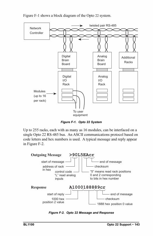
BL1100 Opto 22 Support s 143
Figure F-1 shows a block diagram of the Opto 22 system.
Figure F-1. Opto 22 System
Up to 255 racks, each with as many as 16 modules, can be interfaced on asingle Opto 22 RS-485 bus. An ASCII communications protocol based oncode letters and hex numbers is used. A typical message and reply appearin Figure F-2.
Figure F-2. Opto 22 Message and Response
Network
Controller
twisted pair RS-485
DigitalBrainBoard
DigitalI/ORack
Modules
(up to 16
per rack)
To userequipment
Racks
AnalogBrainBoard
AnalogI/ORack
Additional
>90L5EAcrstart of message
address of rackin hex 5 means read rack positions
0 and 2 correspondingto bits in hex number
checksum
end of message
Outgoing Message
control codeL read analoginputs
Response A1000188889crstart of reply
1000 hexposition 2 value 1888 hex position 0 value
checksum
end of message
BL1100144 s Opto 22 Support
The BL1100 can fit into an Opto 22 network in these ways.
1. The BL1100 can serve as the network controller. Compared to theequivalent Opto 22 controller, the LC4, the BL1100 has severaladvantages.
C programmability allows larger programs to execute muchfaster. The LC4 is programmable only in Basic or Forth.
Direct digital I/O in the controller.
Lower price.
Smaller physical size.
2. The BL1100 can serve as a combination of brain board and digitalrack. The following advantages exist over the equivalent Opto 22equipment.
Lower price and smaller size.
The ability to program the BL1100 to provide local intelligence,which is not possible with the Opto 22 brain board.
The ability to download software to the BL1100 over thenetwork.
If optical isolation is required, then the BL1100 can directly control adigital or an analog rack using the parallel port, replacing the brain boardentirely.
An Opto 22 network usually uses separate transmit and reply twisted pairsbut, if desired, these can be combined in a single twisted pair for communi-cation in both directions. (Separate twisted pairs make it easier to con-struct repeaters.)
RS-485 data communication use a differential voltage to signal a 1 or a 0.This is shown schematically in Figure F-3.
Figure F-3. RS-485 Multiple Receivers
Driver
Tx
Receiver
IntermediateReceiver
+5 V
600 Ω
600 Ω
200 Ω+Tx

BL1100 Opto 22 Support s 145
The diagram shows only the master controller driver and the variousreceivers. Answers from the slaves (brain boards) are returned on anotherline with many drivers and only one receiver at the master controller(Figure F-4).
Figure F-4. RS-485 Multiple Drivers
The driver drives one line high and the other low for a 1. The polarity isreversed for a 0. The receiver is sensitive only to the relative polarity ofthe signals, and has a substantial tolerance (about 12 V) for a shift in theground potential between the driver and receiver. For example, if theground potential changes by 5 V, as might happen between two differentlocations separated by 1000 ft in a factory, the voltages at the driver andreceiver might appear as shown in Table F-2.
The receiver will still detect the correct signal since it only sees that TX isgreater than TX or vice versa.
The resistors shown provide termination and bias for the signal pair. Biasis necessary to prevent noise on the line from toggling the receivers whenno driver is driving the line. The receivers have about 50 mV of hyster-esis. Termination is needed to prevent reflections when a pulse arrives atthe end of the line. If a line is terminated with a resistor equal to the
Driver
Tx
Receiver
IntermediateDriver
600 Ω
200 Ω
600 Ω
150 Ω
+5 V
+Tx
Table F-2. Signal Strengths at Various Locations
Signal At Driver At Receiver
+TX +2.8 V +7.8 V–TX +0.4 V +5.4 V
Reversed Signal At Driver At Receiver
+TX +0.4 V +5.4 V–TX +2.8 V +7.8 V

BL1100146 s Opto 22 Support
characteristic impedance of the line, then no reflection will take place. Theindicated resistor networks are intended for a twisted pair with a character-istic impedance of 100 W (Belden 8261 wire). The effective terminationresistance is 150 W, which is less than the characteristic impedance, andwill cause a reflection equal to 20% of the incoming voltage. The smallreflection is further attenuated, since the wires have a series resistanceamounting to 25 W per 1000 ft for #24 wire. The series resistance attenu-ates reflections that might disturb the signal.
Figure F-5. Twisted Wire Pair for RS-485 Communication
Use Equation (F-1) to compute the transmission line impedance of atwisted pair. Figure F-5 illustrates the variables used in Equation (F-1).
where e is the effective dielectric constant (air = 1). The effective dielectricconstant is somewhere between that of air and the insulator material. If thecapacitance per meter is known, use Equation (F-2).
where C is the capacitance parameter (in picofarads).
The reflection coefficient giving the size of the reflected pulse compared tothe incoming pulse is given by
where Rl is the terminating resistor and R
C is the characteristic impedance
of the line.
dr
C1
C1
RR
RR
+−
(F-1)
××=
r
dln120
e
1R C
(F-2)( )d/rln400,000
CR C ×
=

BL1100 Opto 22 Support s 147
Most twisted pairs will have RC between 50 and 150 W. Larger wires with
thin insulation and a high dielectric constant will have a lower RC. The
propagation velocity will usually be between 50% and 80% of the speed oflight (3.3 ns/m or about a foot per nanosecond). The propagation velocityis proportional to the inverse square root of the dielectric constant.
The higher the RC of the cable and the larger the size of the wire, thefurther the signal can be sent. For #24 wire and RC =100 W, the limit isabout 1000 m or 3300 ft. With #20 wire, this can be extended to about2500 m or 8000 ft without using a repeater.
Figure F-6 shows how to build a cable between a BL1100 and an Opto 22device.
Figure F-6. Cable Between BL1100 and Opto 22 Device
Up to 255 racks, each with as many as 16 modules, can be interfaced on asingle Opto 22 RS-485 bus.
50
1
blue, pin 1
116
Lines 116 are not connected
17 × 2femaleconnector
Pin 1 J010 (VCC) topin 49 on Opto 22 rack
1 2
31 32
.
.
.
J10
Opto 22 connector
1 2J010 Pin 49 (Opto 22) = VCC (J010:1)
Pin 50 (Opto 22) = GND (J010:2)
Pin 47 (Opto 22) = PA0 (J10:1)
Pin 17 (Opto 22) = PB7 (J10:31)Pin 18 (Opto 22) = GND (J10:32)
Split cable into 17 pairs of wiresstarting with 5049 and give eachpair one-half twist to swap signaland GND wire positions.
J010 (2 pins) and J10 (32 pins)make one 34-pin header.

BL1100148 s Opto 22 Support

BL1100 Sample Analog Applications 149
APPENDIX G:SAMPLE ANALOG APPLICATIONS
The demonstrations, or “projects,” in Appendix G explore some sampleapplications for the BL1100’s analog inputs.
BL1100150 s Sample Analog Applications
Semiconductor Temperature SensorThe example in Figure G-1 shows how temperatures can be measuredusing a semiconductor temperature sensor. The resistor network RN3(1 kW resistors) can provide excitation to each of the positive inputs of theop-amps. A jumper must be installed across header J17 to enable excita-tion from the +5 V supply. If the channels are to be excited selectively,then individual pins can be cut on the resistor network.
Figure G-1. Semiconductor Temperature Sensor (100°C to +100°C)
The LM135 temperature sensor measures absolute temperature, starting at0 K or 273°C. Thus, the output is 2.7315 V at a temperature of 0°C. Byusing the 2.5 V reference voltage to offset the op-amp in a differentialconfiguration, the zero point is shifted to 250 K or 23.15°C. The 10 kWresistor at R
4 provides a gain of 1.8181. The A/D converter accepts inputs
from 2.5 V to +2.5 V. The A/D output is a 10-bit number from 512 to+511. (A value of +512, which cannot occur, corresponds to +2.5 V.) Thenet result is that the output of the A/D converter is 86 counts at 0°C, and is459 counts at 100°C. The temperature in degrees Celsius can be easilycalculated with Equation (G-1).
These coefficients can be adjusted by a calibration procedure for eachindividual temperature sensor and amplifier.
+
To A/D Converter
Sensitivity is3.73 counts/°C
R1 = 10 kΩ
R3 = 10 kΩ
R4 = 10 kΩ
1 kΩ
+5 V
+5 V
5 V
LM13510 mV/K
+2.5 V ref
R2 = 100 kΩ
(G-1)outputAD0.26855 -23.15
outputAD1024
275 -23.15TC
×+=
×
+=

BL1100 Sample Analog Applications s 151
+
To A/D Converter
ColdJunction +5 V
R4 = 1 MΩ
R3 = 10 kΩ
R1 = 10 kΩ
5 V
R2 = 1 MΩ
ThermocoupleA thermocouple generates small voltages, about 40 µV/°C for a copper-nickel thermocouple. The circuit in Figure G-2 uses a gain of 100 toamplify the small voltages to about 4 mV/°C.
FigureG-2. Thermocouple
The cold junction can be at the point where the thermocouple wiresconnect to the BL1100. Since the thermocouple measures the difference intemperature between the cold junction and the other junction, an indepen-dent temperature measurement device is needed at the cold junction. Theonboard temperature sensor can be used if it has sufficient accuracy for theapplication. The offset in the amplifier and the nonlinearity of the thermo-couple can both be compensated in software. A capacitor may be addedacross R
4 as a part of an input filter.
BL1100152 s Sample Analog Applications
420 mA LoopMany industrial-style sensors use 420 mA loops. The sensor is poweredby the current loop and reports the value sensed by modulating the amountof current flowing in the loop. A circuit such as the one shown inFigure G-3 can be used to obtain the loop current. External power and anexternal 68 W resistor are used. The 68 W resistor can often be mountedon the field-wiring terminal block. This circuit gives 2.47 V for a full-scale reading.
Figure G-3. 420 mA Loop
+
+24 V
To A/DConverter
4-20 mASensor
68 Ω
R1 = 10 kΩ
R3 = 10 kΩ
R2 = 100 kΩ+5 V
R4 = 10 kΩ
5 V

BL1100 PLCBus 153
APPENDIX H: PLCBUS
Appendix H provides the pin assignments for the PLCBus, describes theregisters, and lists the software drivers.
BL1100154 s PLCBus
OverviewThe PLCBus is a general-purpose expansion bus for Z-World controllers.The PLCBus is available on the BL1200, BL1600, BL1700, PK2100, andPK2200 controllers. The BL1100 supports the XP8300, XP8400,XP8600, XP8900, and Exp-A/D12 expansion boards using the controllersparallel input/output port.
The BL1100 also has a series of expansion boards exclusive tothe BL1100. These boards and their use are described inAppendix I.
Table H-1 lists all Z-World expansion devices that are supported on thePLCBus.
Multiple expansion boards maybe linked together and con-nected to a Z-World controllerto form an extended system.
Figure H-1 shows the pin layoutfor the PLCBus connector.
Table H-1. Z-World PLCBus Expansion Devices
Device Description
Exp-A/D12 Eight channels of 12-bit A/D converters
SE1100 Four SPDT relays for use with all Z-World controllers
XP8100 Series 32 digital inputs/outputs
XP8200 “Universal Input/Output Board”—16 universal inputs, 6 high-current digital outputs
XP8300 Two high-power SPDT and four high-power SPST relays
XP8400 Eight low-power SPST DIP relays
XP8500 11 channels of 12-bit A/D converters
XP8600 Two channels of 12-bit D/A converters
XP8700 One full-duplex asynchronous RS-232 port
XP8800 One-axis stepper motor control
XP8900 Eight channels of 12-bit D/A converters
24
13
6 58 7
10 912 1114 1316 1518 1720 1922 2124 2326 25
GNDD7XD5XD3XD1X
LCDXA0X
GND
GND attention /ATstrobe /STBXGNDA3XGNDA2XGNDA1X
/RDXVCC (+5 V)
D0X/WRX
D4XD2X
D6X
+24 V(+5 V) VCC
Figure H-1. PLCBus Pin Diagram
$
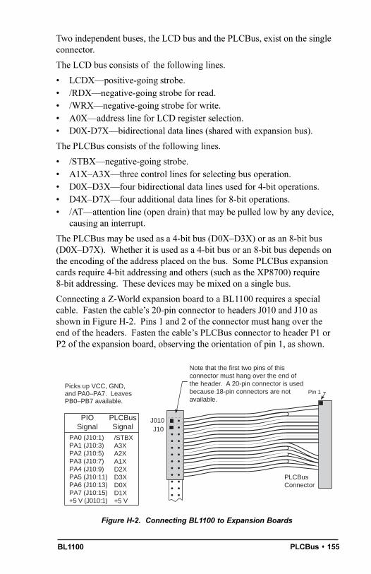
BL1100 PLCBus s 155
Two independent buses, the LCD bus and the PLCBus, exist on the singleconnector.
The LCD bus consists of the following lines.
LCDXpositive-going strobe. /RDXnegative-going strobe for read. /WRXnegative-going strobe for write. A0Xaddress line for LCD register selection. D0X-D7Xbidirectional data lines (shared with expansion bus).
The PLCBus consists of the following lines.
/STBXnegative-going strobe. A1XA3Xthree control lines for selecting bus operation. D0XD3Xfour bidirectional data lines used for 4-bit operations. D4XD7Xfour additional data lines for 8-bit operations. /ATattention line (open drain) that may be pulled low by any device,
causing an interrupt.
The PLCBus may be used as a 4-bit bus (D0XD3X) or as an 8-bit bus(D0XD7X). Whether it is used as a 4-bit bus or an 8-bit bus depends onthe encoding of the address placed on the bus. Some PLCBus expansioncards require 4-bit addressing and others (such as the XP8700) require8-bit addressing. These devices may be mixed on a single bus.
Connecting a Z-World expansion board to a BL1100 requires a specialcable. Fasten the cables 20-pin connector to headers J010 and J10 asshown in Figure H-2. Pins 1 and 2 of the connector must hang over theend of the headers. Fasten the cables PLCBus connector to header P1 orP2 of the expansion board, observing the orientation of pin 1, as shown.
Figure H-2. Connecting BL1100 to Expansion Boards
Pin 1
PA0 (J10:1)PA1 (J10:3)PA2 (J10:5)PA3 (J10:7)PA4 (J10:9)PA5 (J10:11)PA6 (J10:13)PA7 (J10:15)+5 V (J010:1)
/STBXA3XA2XA1XD2XD3XD0XD1X+5 V
PIOSignal
PLCBusSignal
Picks up VCC, GND,and PA0–PA7. LeavesPB0–PB7 available.
J010
PLCBusConnector
Note that the first two pins of thisconnector must hang over the end ofthe header. A 20-pin connector is usedbecause 18-pin connectors are notavailable.
J10
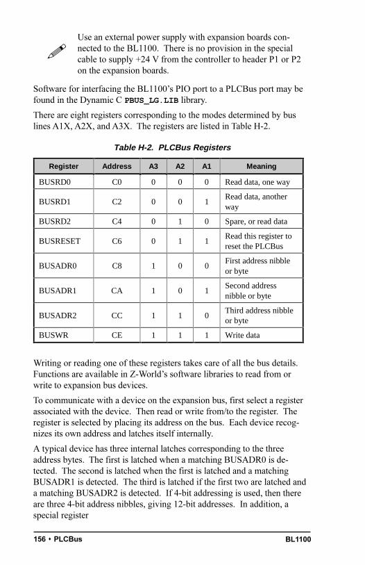
BL1100156 s PLCBus
Table H-2. PLCBus Registers
Register Address A3 A2 A1 Meaning
BUSRD0 C0 0 0 0 Read data, one way
BUSRD1 C2 0 0 1Read data, anotherway
BUSRD2 C4 0 1 0 Spare, or read data
BUSRESET C6 0 1 1Read this register toreset the PLCBus
BUSADR0 C8 1 0 0First address nibbleor byte
BUSADR1 CA 1 0 1Second addressnibble or byte
BUSADR2 CC 1 1 0Third address nibbleor byte
BUSWR CE 1 1 1 Write data
Use an external power supply with expansion boards con-nected to the BL1100. There is no provision in the specialcable to supply +24 V from the controller to header P1 or P2on the expansion boards.
Software for interfacing the BL1100s PIO port to a PLCBus port may befound in the Dynamic C PBUS_LG.LIB library.
There are eight registers corresponding to the modes determined by buslines A1X, A2X, and A3X. The registers are listed in Table H-2.
Writing or reading one of these registers takes care of all the bus details.Functions are available in Z-Worlds software libraries to read from orwrite to expansion bus devices.
To communicate with a device on the expansion bus, first select a registerassociated with the device. Then read or write from/to the register. Theregister is selected by placing its address on the bus. Each device recog-nizes its own address and latches itself internally.
A typical device has three internal latches corresponding to the threeaddress bytes. The first is latched when a matching BUSADR0 is de-tected. The second is latched when the first is latched and a matchingBUSADR1 is detected. The third is latched if the first two are latched anda matching BUSADR2 is detected. If 4-bit addressing is used, then thereare three 4-bit address nibbles, giving 12-bit addresses. In addition, aspecial register
!
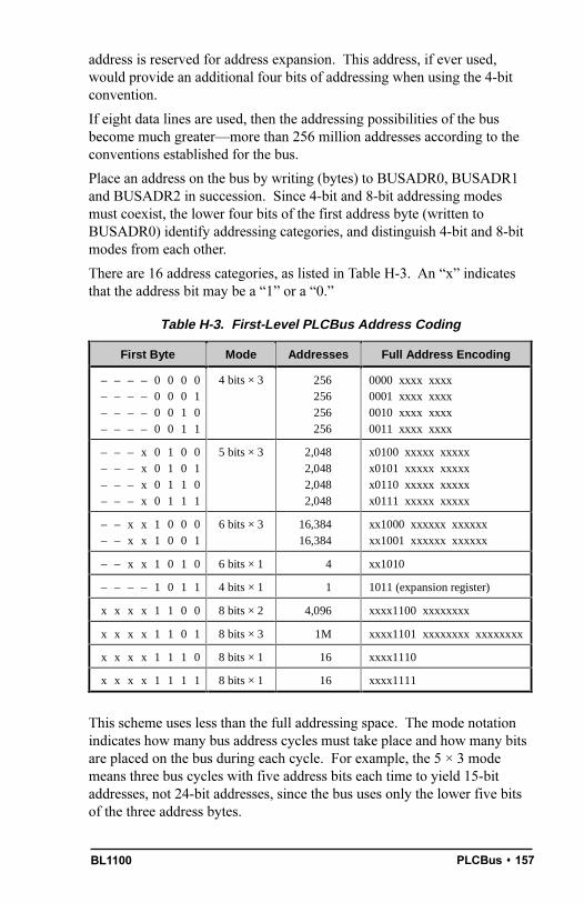
BL1100 PLCBus s 157
Table H-3. First-Level PLCBus Address Coding
First Byte Mode Addresses Full Address Encoding
– – – – 0 0 0 0– – – – 0 0 0 1– – – – 0 0 1 0– – – – 0 0 1 1
4 bits × 3 256256256256
0000 xxxx xxxx0001 xxxx xxxx0010 xxxx xxxx0011 xxxx xxxx
– – – x 0 1 0 0– – – x 0 1 0 1– – – x 0 1 1 0– – – x 0 1 1 1
5 bits × 3 2,0482,0482,0482,048
x0100 xxxxx xxxxxx0101 xxxxx xxxxxx0110 xxxxx xxxxxx0111 xxxxx xxxxx
– – x x 1 0 0 0– – x x 1 0 0 1
6 bits × 3 16,38416,384
xx1000 xxxxxx xxxxxxxx1001 xxxxxx xxxxxx
– – x x 1 0 1 0 6 bits × 1 4 xx1010
– – – – 1 0 1 1 4 bits × 1 1 1011 (expansion register)
x x x x 1 1 0 0 8 bits × 2 4,096 xxxx1100 xxxxxxxx
x x x x 1 1 0 1 8 bits × 3 1M xxxx1101 xxxxxxxx xxxxxxxx
x x x x 1 1 1 0 8 bits × 1 16 xxxx1110
x x x x 1 1 1 1 8 bits × 1 16 xxxx1111
address is reserved for address expansion. This address, if ever used,would provide an additional four bits of addressing when using the 4-bitconvention.
If eight data lines are used, then the addressing possibilities of the busbecome much greatermore than 256 million addresses according to theconventions established for the bus.
Place an address on the bus by writing (bytes) to BUSADR0, BUSADR1and BUSADR2 in succession. Since 4-bit and 8-bit addressing modesmust coexist, the lower four bits of the first address byte (written toBUSADR0) identify addressing categories, and distinguish 4-bit and 8-bitmodes from each other.
There are 16 address categories, as listed in Table H-3. An x indicatesthat the address bit may be a 1 or a 0.
This scheme uses less than the full addressing space. The mode notationindicates how many bus address cycles must take place and how many bitsare placed on the bus during each cycle. For example, the 5 × 3 modemeans three bus cycles with five address bits each time to yield 15-bitaddresses, not 24-bit addresses, since the bus uses only the lower five bitsof the three address bytes.

BL1100158 s PLCBus
SHBUS1 SHBUS1+1SHBUS0 SHBUS0+1 SHBUS0+2 SHBUS0+3
Bus expansion BUSADR0 BUSADR1 BUSADR2
Table H-4. Allocation of Registers
A1 A2 A3 Meaning
000j 000j xxxjdigital output registers, 64 registers64 × 8 = 512 1-bit registers
000j 001j xxxj analog output modules, 64 registers
000j 01xj xxxjdigital input registers, 128 registers128 × 4 = 512 input bits
000j 10xj xxxj analog input modules, 128 registers
000j 11xj xxxj 128 spare registers (customer)
001j xxxj xxxj 512 spare registers (Z-World)
j controlled by board jumperx controlled by PAL
Z-World provides software drivers that access the PLCBus. To allowaccess to bus devices in a multiprocessing environment, the expansionregister and the address registers are shadowed with memory locationsknown as shadow registers. The 4-byte shadow registers, which are savedat predefined memory addresses, are as follows.
Before the new addresses or expansion register values are output to thebus, their values are stored in the shadow registers. All interrupts that usethe bus save the four shadow registers on the stack. Then, when exiting theinterrupt routine, they restore the shadow registers and output the threeaddress registers and the expansion registers to the bus. This allows aninterrupt routine to access the bus without disturbing the activity of abackground routine that also accesses the bus.
To work reliably, bus devices must be designed according to the followingrules.
1. The device must not rely on critical timing such as a minimum delaybetween two successive register accesses.
2. The device must be capable of being selected and deselected withoutadversely affecting the internal operation of the controller.
Allocation of Devices on the Bus
4-Bit DevicesTable H-4 provides the address allocations for the registers of 4-bit devices.

BL1100 PLCBus s 159
Table H-5. Dynamic C PLCBus Libraries
Library Needed Controller
DRIVERS.LIB All controllers
EZIOTGPL.LIB BL1000
EZIOLGPL.LIB BL1100
EZIOMGPL.LIB BL1400, BL1500
EZIOPLC.LIB BL1200, BL1600, PK2100, PK2200, ZB4100
EZIOPLC2.LIB BL1700
PBUS_TG.LIB BL1000
PBUS_LG.LIB BL1100, BL1300
PLC_EXP.LIB BL1200, BL1600, PK2100, PK2200
Digital output devices, such as relay drivers, should be addressed withthree 4-bit addresses followed by a 4-bit data write to the control register.The control registers are configured as follows
bit 3 bit 2 bit 1 bit 0A2 A1 A0 D
The three address lines determine which output bit is to be written. Theoutput is set as either 1 or 0, according to D. If the device exists on thebus, reading the register drives bit 0 low. Otherwise bit 0 is a 1.
For digital input, each register (BUSRD0) returns four bits. The readregister, BUSRD1, drives bit 0 low if the device exists on the bus.
8-Bit DevicesZ-Worlds XP8700 and XP8800 expansion boards use 8-bit addressing.Refer to the XP8700 and XP8800 manual.
Expansion Bus SoftwareThe expansion bus provides a convenient way to interface Z-Worldscontrollers with expansion boards or other specially designed boards. Theexpansion bus may be accessed by using input functions. Follow thesuggested protocol. The software drivers are easier to use, but are lessefficient in some cases. Table H-5 lists the libraries.
BL1100160 s PLCBus
There are 4-bit and 8-bit drivers. The 4-bit drivers employ the followingcalls.
void eioResetPlcBus()
Resets all expansion boards on the PLCBus. When using this call,make sure there is sufficient delay between this call and the first accessto an expansion board.
LIBRARY: EZIOPLC.LIB, EZIOPLC2.LIB, EZIOMGPL.LIB.
void eioPlcAdr12( unsigned addr )
Specifies the address to be written to the PLCBus using cyclesBUSADR0, BUSADR1, and BUSADR2.
PARAMETER: addr is broken into three nibbles, and one nibble iswritten in each BUSADRx cycle.
LIBRARY: EZIOPLC.LIB, EZIOPLC2.LIB, EZIOMGPL.LIB.
void set16adr( int adr )
Sets the current address for the PLCBus. All read and write operationsaccess this address until a new address is set.
PARAMETER: adr is a 16-bit physical address. The high-ordernibble contains the value for the expansion register, and the remainingthree 4-bit nibbles form a 12-bit address (the first and last nibbles mustbe swapped).
LIBRARY: DRIVERS.LIB.
void set12adr( int adr )
Sets the current address for the PLCBus. All read and write operationsaccess this address until a new address is set.
PARAMETER: adr is a 12-bit physical address (three 4-bit nibbles)with the first and third nibbles swapped.
LIBRARY: DRIVERS.LIB.
void eioPlcAdr4( unsigned addr )
Specifies the address to be written to the PLCBus using only cycleBUSADR2.
PARAMETER: addr is the nibble corresponding to BUSADR2.
LIBRARY: EZIOPLC.LIB, EZIOPLC2.LIB, EZIOMGPL.LIB.
BL1100 PLCBus s 161
void set4adr( int adr )
Sets the current address for the PLCBus. All read and write operationsaccess this address until a new address is set.
A 12-bit address may be passed to this function, but only the last fourbits will be set. Call this function only if the first eight bits of theaddress are the same as the address in the previous call to set12adr.
PARAMETER: adr contains the last four bits (bits 811) of thephysical address.
LIBRARY: DRIVERS.LIB.
char _eioReadD0( )
Reads the data on the PLCBus in the BUSADR0 cycle.
RETURN VALUE: the byte read on the PLCBus in the BUSADR0cycle.
LIBRARY: EZIOPLC.LIB, EZIOPLC2.LIB, EZIOMGPL.LIB.
char _eioReadD1( )
Reads the data on the PLCBus in the BUSADR1 cycle.
RETURN VALUE: the byte read on the PLCBus in the BUSADR1cycle.
LIBRARY: EZIOPLC.LIB, EZIOPLC2.LIB, EZIOMGPL.LIB.
char _eioReadD2( )
Reads the data on the PLCBus in the BUSADR2 cycle.
RETURN VALUE: the byte read on the PLCBus in the BUSADR2cycle.
LIBRARY: EZIOPLC.LIB, EZIOPLC2.LIB, EZIOMGPL.LIB.
char read12data( int adr )
Sets the current PLCBus address using the 12-bit adr, then reads fourbits of data from the PLCBus with BUSADR0 cycle.
RETURN VALUE: PLCBus data in the lower four bits; the upper bitsare undefined.
LIBRARY: DRIVERS.LIB.
BL1100162 s PLCBus
char read4data( int adr )
Sets the last four bits of the current PLCBus address using adr bits 811, then reads four bits of data from the bus with BUSADR0 cycle.
PARAMETER: adr bits 811 specifies the address to read.
RETURN VALUE: PLCBus data in the lower four bits; the upper bitsare undefined.
LIBRARY: DRIVERS.LIB.
void _eioWriteWR( char ch)
Writes information to the PLCBus during the BUSWR cycle.
PARAMETER: ch is the character to be written to the PLCBus.
LIBRARY: EZIOPLC.LIB, EZIOPLC2.LIB, EZIOMGPL.LIB.
void write12data( int adr, char dat )
Sets the current PLCBus address, then writes four bits of data to thePLCBus.
PARAMETER: adr is the 12-bit address to which the PLCBus is set.
dat (bits 03) specifies the data to write to the PLCBus.
LIBRARY: DRIVERS.LIB.
void write4data( int address, char data )
Sets the last four bits of the current PLCBus address, then writes fourbits of data to the PLCBus.
PARAMETER: adr contains the last four bits of the physical address(bits 811).
dat (bits 03) specifies the data to write to the PLCBus.
LIBRARY: DRIVERS.LIB.
The 8-bit drivers employ the following calls.
void set24adr( long address )
Sets a 24-bit address (three 8-bit nibbles) on the PLCBus. All read andwrite operations will access this address until a new address is set.
PARAMETER: address is a 24-bit physical address (for 8-bit bus)with the first and third bytes swapped (low byte most significant).
LIBRARY: DRIVERS.LIB.
BL1100 PLCBus s 163
void set8adr( long address )
Sets the current address on the PLCBus. All read and write operationswill access this address until a new address is set.
PARAMETER: address contains the last eight bits of the physicaladdress in bits 1623. A 24-bit address may be passed to this function,but only the last eight bits will be set. Call this function only if the first16 bits of the address are the same as the address in the previous call toset24adr.
LIBRARY: DRIVERS.LIB.
int read24data0( long address )
Sets the current PLCBus address using the 24-bit address, then readseight bits of data from the PLCBus with a BUSRD0 cycle.
RETURN VALUE: PLCBus data in lower eight bits (upper bits 0).
LIBRARY: DRIVERS.LIB.
int read8data0( long address )
Sets the last eight bits of the current PLCBus address using address bits1623, then reads eight bits of data from the PLCBus with a BUSRD0cycle.
PARAMETER: address bits 1623 are read.
RETURN VALUE: PLCBus data in lower eight bits (upper bits 0).
LIBRARY: DRIVERS.LIB.
void write24data( long address, char data )
Sets the current PLCBus address using the 24-bit address, then writeseight bits of data to the PLCBus.
PARAMETERS: address is 24-bit address to write to.
data is data to write to the PLCBus.
LIBRARY: DRIVERS.LIB.
void write8data( long address, char data )
Sets the last eight bits of the current PLCBus address using address bits1623, then writes eight bits of data to the PLCBus.
PARAMETERS: address bits 1623 are the address of the PLCBusto write.
data is data to write to the PLCBus.
LIBRARY: DRIVERS.LIB.

BL1100164 s PLCBus

Simulated PLCBus Connection 165BL1100
APPENDIX I:SIMULATED PLCBUS CONNECTION
Certain standard Z-World expansion boards may be used with the BL1100,as explained in Appendix H. Appendix I explains how to make a simulatedPLCBus connected using the PIO header on the BL1100. Selectedsoftware functions are also described.

166 s Simulated PLCBus Connection BL1100
PIO Port Connections
Standard Z-World Expansion BoardsExpansion boards may be connected to header J010/J10 on the BL1100.To add expansion boards, the user must make a custom cable (Z-Worldpart number 540-0015). To assist with making the connection via acustom-made ribbon cable, the table in Figure I-1 maps the signals fromthe controllers PIO to the expansion board PLCBus header. Fasten thecables 20-pin connector to the combined headers J010 and J10 as shownin Figure I-1. Pins 1 and 2 of the custom cable connector must hang overthe end of the combined headers. Fasten the cables PLCBus connector toexpansion board header P1 or P2. Note the orientation of pin 1.
Figure I-1. BL1100 Expander Cable Connection
Software for interfacing the BL1100s PIO port to a PLCBus port may befound in the Dynamic C EZIOMGPL.LIB library (for XP8900 Series ex-pansion boards) or the PBUS_LG.LIB library.
Use an external power supply when connecting expansionboards to the BL1100. There is no provision in the customcable to supply +24 V from the controller to header P1 or P2on the expansion board.
Pin 1
PA0 (J10:1)PA1 (J10:3)PA2 (J10:5)PA3 (J10:7)PA4 (J10:9)PA5 (J10:11)PA6 (J10:13)PA7 (J10:15)+5 V (J010:1)
/STBXA3XA2XA1XD2XD3XD0XD1X+5 V
PIOSignal
PLCBusSignal
Picks up VCC, GND,and PA0–PA7. LeavesPB0–PB7 available.
J010
PLCBusConnector
Note that the first two pins of thisconnector must hang over the end ofthe header. A 20-pin connector is usedbecause 18-pin connectors are notavailable.
J10
!
Simulated PLCBus Connection s 167BL1100
Software Drivers
Using Expansion Boards with PIO 1 Port AA PLCBus driver is implemented using the 8-bit PIO 1 Port A (PIOA).With the BL1100, the developer is limited to 4-bit PLCBus peripherals.An attention line (/AT) is not available. The wiring connections shown inFigure I-1 are used.
General-Purpose Drivers
void PBus12_Addr( int addr )
Sets the current address for the PLCBus. All read and write operationswill access this address until a new address is set.
PARAMETER: addr is the 12-bit physical address, with the first andthird nibbles swapped (the most significant nibble is in the low fourbits).
RETURN VALUE: None.
void PBus4_Write( char data )
Writes 4-bit data on PLCBus. The address must be set by a call toPBus12_Addr before calling this function.
PARAMETER: data should contain the value to write in the lowerfour bits.
RETURN VALUE: None.
int PBus4_Read0( )
Reads 4 bits of data from the PLCBus using a BUSRD0 cycle. Theaddress must be set by a call to PBus12_Addr before calling thisfunction.
RETURN VALUE: PLCBus data in the lower 4 bits (the upper bits areundefined).
int PBus4_Read1( )
Reads 4 bits of data from the PLCBus using a BUSRD1 cycle. Theaddress must be set by a call to PBus12_Addr before calling thisfunction.
RETURN VALUE: PLCBus data in the lower 4 bits (the upper bits areundefined).

168 s Simulated PLCBus Connection BL1100
int PBus4_ReadSp( )
Reads 4 bits of data from the PLCBus using a BUSSPARE cycle. Theaddress must be set by a call to PBus12_Addr before calling thisfunction.
RETURN VALUE: PLCBus data in the lower 4 bits (the upper bits areundefined).
void Reset_PBus( )
Resets the PLCBus.
RETURN VALUE: None.
int Poll_PBus_Node( int addr )
Polls a PLCBus device by performing a BUSRD0 cycle and checkingthe low bit of the returned value.
PARAMETER: addr is the 12-bit physical address of the device, withthe first and third nibbles swapped.
RETURN VALUE: Returns 1 if node answers poll, 0 if not.
void Reset_PBus_Wait( )
Provides the minimum delay necessary for PLCBus expansion boardsafter a bus reset, using a 9 MHz CPU. This delay will be insufficientfor a faster CPU, and must be increased.
RETURN VALUE: None.
Relay Expansion Board Drivers
int Relay_Board_Addr( int board )
Converts a logical relay board address to a physical PLCBus address.
PARAMETER: board must be a number between 0 and 63 represent-ing the relay board to access. This number has the binary form pppzyx,where ppp is determined by the board PAL number, and x, y, and z aredetermined by jumpers on header J1 on the expansion board.
ppp values of 000, 001, 010,, correspond to PAL numbers ofFPO4500, FPO4510, FPO4520,
x, y, and z correspond to a jumper across J1 pins 12, 34, and 56respectively (0 = closed, 1 = open). The resulting address is in the formpppx000y000z.
RETURN VALUE: The PLCBus address of the board specified, withthe first and third nibbles swapped. This address may be passeddirectly to PBus12_Addr.

Simulated PLCBus Connection s 169BL1100
void Set_PBus_Relay( int board, int relay,int state )
Sets a relay on an expansion bus relay board.
PARAMETER: board must be a number between 0 and 63 represent-ing the relay board to access. This number has the binary form pppzyx,where ppp is determined by the board PAL number, and x, y, and z aredetermined by jumpers on header J1 on the expansion board.
ppp values of 000, 001, 010,, correspond to PAL numbers ofFPO4500, FPO4510, FPO4520,
x, y, and z correspond to a jumper across J1 pins 12, 34, and 56respectively (0 = closed, 1 = open).
relay is the relay number on the board (05 for XP8300, 07 forXP8400).
state must be 1 to turn the relay on and 0 to turn the relay off.
RETURN VALUE: None.
D/A Converter Expansion Board Drivers
int DAC_Board_Addr( int bd )
Converts a logical DAC board address to a physical PLCBus address.
PARAMETER: bd must be a number between 0 and 63 representingthe DAC board to access. This number has the binary form pppzyxwhere ppp is determined by the board PAL number, and x, y, and z aredetermined by jumpers on header J3 on the expansion board.
ppp values of 000, 001, 010,, correspond to PAL numbers ofFPO4800, FPO4810, FPO4820,
x, y, and z correspond to a jumper across J3 pins 12, 34, and 56respectively (0 = closed, 1 = open). The resulting address is in theform pppx001y000z.
RETURN VALUE: The PLCBus address of the board specified, withthe first and third nibbles swapped. This address may be passeddirectly to PBus12_Addr.
void Write_DAC1( int val )
Loads Register A of DAC #1 with the given 12-bit value. The boardaddress must have been set previously with a call to PBus12_Addr.The value in val will not actually be output until Latch_DAC1 iscalled.
RETURN VALUE: None.
170 s Simulated PLCBus Connection BL1100
void Write_DAC2( int val )
Loads Register A of DAC #2 with the given 12-bit value. The boardaddress must have been set previously with a call to PBus12_Addr.The value in val will not actually be output until Latch_DAC2 is called.
RETURN VALUE: None.
void Latch_DAC1( )
Moves the value from Register A of DAC #1 to Register B. The valuein Register B represents the actual DAC output. The board addressmust have been set previously with a call to PBus12_Addr, and thevalue should have been loaded into Register A with a call to Write_DAC1.
RETURN VALUE: None.
void Latch_DAC2( )
Moves the value from Register Aof DAC #2 to Register B. The valuein Register B represents the actual DAC output. The board addressmust have been set previously with a call to PBus12_Addr, and thevalue should have been loaded into Register A with a call to Write_DAC2.
RETURN VALUE: None.
void Init_DAC( )
Initializes DAC board and sets all output values to 0. Call this functionbefore writing data to the DAC. The board address must have been setpreviously with a call to PBus12_Addr.
RETURN VALUE: None.
void Set_DAC1( int val )
Sets DAC #1 to the value specified in the lower 12 bits of val. In thevoltage output mode (J1 pins 23 jumpered), Vout = (val/4096) *10.22 V with the Z-World default settings. In the current output mode(J1 pins 12 jumpered), Iout = (val/4096) * 22 mA with the Z-Worlddefault settings. The board address must have been set previously witha call to PBus12_Addr.
RETURN VALUE: None.
void Set_DAC2( int val )
Sets DAC #2 to the value specified in the lower 12 bits of val. In thevoltage output mode (J1 pins 23 jumpered), Vout = (val/4096) *10.22 V with the Z-World default settings. In the current output mode(J1 pins 12 jumpered), Iout = (val/4096) * 22 mA with the Z-Worlddefault settings. The board address must have been set previously witha call to PBus12_Addr.
RETURN VALUE: None.
BL1100 Standalone Operation 171
APPENDIX J: STANDALONE OPERATION
Appendix J provides information about running the BL1100 after it isprogrammed, burning EPROMs, and downloading software remotely.
BL1100172 s Standalone Operation
There are two ways to run an application with the BL1100 disconnectedfrom the PC. The application may either be burned into a new EPROM totake the place of the existing Dynamic C EPROM, or it can run from(battery-backed) static RAM.
There are a few considerations when running an application as a standa-lone program.
1. To run correctly, the code should not have any printf, putchar,getchar, or kbhit function calls. These attempt to talk to the PC andwill lock up the program in a standalone mode.
2. Defined constants (for example, float pi = 3.141593;) will nowbe truly constant for EPROM-based applications, since they are burnedin. In a RAM-based application, constants are be initially downloadedwith their declared value, but can be modified by software. That is, thestatement pi = 1.0; will affect a RAM-based application, but not anEPROM-based one.
3. The timing of the application will change. Since the application is nolonger connected to Dynamic C, it will run a little faster. Debuggingcode will not be loaded into EPROM (or RAM if the nodebug optionis used). Be especially careful when any hardware interfacing dependson timing.
4. It is possible, although rare, for a program not to run out of ROM whenit could run out of RAM. This is because of the complex pagingscheme used by the compiler to manage code and data spaces in theinteractive environment. This should not be a problem in smallprograms.
Option 1: Burn an EPROMA program may be burned into a new EPROM chip that then replacesthe Dynamic C EPROM on the controller. This requires an EPROMburner and a blank EPROM.
1. Compile the program to an .ROM file by selecting the Compile to Fileoption in the COMPILE menu. The BL1000 must be connected to thePC running Dynamic C during this step because essential libraryroutines must be uploaded from the Dynamic C EPROM and linked tothe resulting file. The output is a binary file or an Intel hex format filewith the program name and an .ROM extension.
2. Exit Dynamic C.
3. Use the binary or the hex format file to burn an EPROM with anEPROM burner. Refer to the burner instructions for specific informa-tion on this.

BL1100 Standalone Operation s 173
4. Replace the Dynamic C EPROM on the board with the new one. If thenew EPROM has s different size than the Dynamic C EPROM, ajumper on the BL1000 may need to be moved.
5. When power is applied to the board, the new program will havecomplete control. As far as the controller is concerned, Dynamic C nolonger exists.
Option 2: Use Battery-Backed Static RAMWhen a program is compiled from a PC, it is actually stored in the staticRAM and executed from there. Since the RAM has a battery to keep thecode intact, the code will remain in the board even when power is re-moved.
1. Compile the program to RAM in the usual manner. If the codecompiles with no errors, the watch window pop up. Dynamic C stillassumes that the program will run with the PC attached.
2. Set the appropriate jumpers on the board to indicate to Dynamic C thatthe BL1100 will now run in standalone mode from static RAM.
3. Press the RESET button on the controller or cycle power off-on.
4. The program will start running and break off communication with thePC. A message on the PC will indicate that communication was lost.(The PC has no way of knowing that the above events took place. Itjust sees that communication with the controller has stopped.)
5. The controller may now be disconnected from the PC.
ReliabilitySince an EPROM is a read-only device, the program cannot be acciden-tally written over because of a software bug. Code and data in RAM,however, does incur the risk of being overwritten. A misused pointer or astack overflow can cause a program to overwrite itself.
Program LifeAn EPROM-based program is, for practical purposes, permanent. Pro-grams in battery-backed RAM have an indefinitely long life unless thebattery dies. A batterys life is around 3 power-off years. The batterydoes not discharge significantly with power applied. If the controller isnever powered down, then the program essentially lasts forever. Rarely,the RAM or EPROM chips can fail. This possibility could be taken intoconsideration for long-term use.
BL1100174 s Standalone Operation
SpeedDebugger information a RAM-based program is not present in anEPROM-based program since the compiler knows that a program inEPROM will not be using the Dynamic C interface. This results in a slightincrease in performance for EPROM-based programs.
The nodebug option may be used in a program to eliminatethis difference. Debugging information will not be stored inRAM. But it will not be possible to debug the programinteractively from a PC. Refer to the Dynamic C manuals fordetails.
Data SpaceUsing an EPROM to store code (and constants) leaves more space in theRAM to hold variable data.
CostA typical PC-based EPROM burner costs several hundred dollars. AnEPROM eraser can be found for around $50. On the other hand, the staticRAM is already paid for. No other accessories are necessary to executecode out of RAM.
EaseFor developing a single board, it is easier and quicker to run from RAM.For volume applications, it will become very tedious to connect eachcontroller to the PC and compile code into it.
Remote DownloadingCode based in RAM can be modified by an outside source. An example ofthis is a remote connection through a modem where new code could bedownloaded to the controller and executed. In this case, a monitorprogram, burned into ROM, is needed to serve as a master controller toload and start execution of the programs and to receive control when theexecuted program finishes.
The monitor program also gains control if the board is reset throughhardware, either by power-on, watchdog timeout, or reset. An externalhardware reset line can also be installed so that the computer that isdownloading the program can force a hardware reset of the as a sure wayof gaining control. Install an external hardware reset by using one of theRS-485 handshaking lines (CTS or RXC). The output of the receiver forthe line chosen can be connected to the same reset line as the reset push-button. Then the external input will be a direct reset.
!
BL1100 Standalone Operation s 175
Review the memory map and program format before writing a monitorprogram for downloading software. Figure H-1 shows the EPROMmemory layout. All changeable data areas are in upper memory and mustalways be in RAM. The user program can be in EPROM or in RAM,beginning with the interrupt vectors. The BIOS is always in EPROM.
The 64K space shown in Figure J-1 is the code space visible to themicroprocessor. The memory management unit of the Z180, which isbetween the microprocessor and physical memory, can address 1 M ofmemory.
Figure J-1. EPROM Memory Layout
See Appendix C, Memory, I/O Map, and Interrupt Vectors,for details on memory management.
Library RAM
free memory
heap
user programstatic data
system stack
aux stack
user program andinitialized data
environmentalconstants
pointer storecheck table
startup code
0000
2000
2100
2300
2200
2340
FFFF
interrupt vectors
library anddebug kernel
Sizes set bymemory mapoptions inDynamic C
unused
$

BL1100176 s Standalone Operation
The ROM chip occupies the space from 0 to 256K in the physical memory.If a ROM is smaller than 256K, data will seem to appear at multipleaddresses. If, for example, a ROM has the standard 32K, ROM addressesare evaluated modulo 32K. Each datum appears at eight addresses.
The RAM chip occupies the space from 256K to 768K (40000 to BFFFFhex). Once again, the contents of the RAM will be appear to be repeatedin the allocated space unless a 512K RAM chip is installed. The top of theRAM spacethe last image of the RAM contentsis always mapped tothe top of the logical 64K microprocessor code space.
To download and run a program, burn the monitor program into EPROM.When the BL1100 powers up, it automatically executes the monitorprogram, which can then download the program, storing the program inRAM. Part of the BL1100 RAM is mapped out of the microprocessorspace, but it can be accessed by using the DMA block copy feature. Oncethe program is in memory, the monitor program will change the memorymapping registers and jump to the startup code for the downloadedprogram. This can be made to happen by copying a small routine to highmemory and then jumping to that routine. This is code that actuallychanges the memory mapping registers and jumps to the startup code.
It is possible for the program running in RAM to return to the monitorprogram by a similar trick in reverse. By manipulating the size of freememory (in the OPTIONS menu), the data spaces of the programs can beassigned separate memory areas. It is also possible to have shared dataareas by careful attention to data declarations. Data declarations consumememory in reverse order of their declaration. The data area grows down,although each array or structure is defined in a forward direction inmemory.
A major application for downloading programs is distributed processingsystems that are subject to frequent software updates or which need to beconfigured differently depending on the site or the application. In somecases, it may simpler or more convenient to download the software.
If the downloaded program will not return control to the monitor program,then the BL1100 has to be reset externally. If a separate reset line is notavailable and the power cannot be interrupted to reset the BL1100, then itis necessary to take elaborate precautions against the possibility of theBL1100 losing communication with the base computer. This could happenif a software fault or a transient electrical disturbance causes the BL1100to enter an endless loop and stop communicating. If the BL11To write amonitor program for downloading software, you must understand thememory map and program format. The diagram following shows the layoutof the memory for EPROM. All changeable data areas are in uppermemory and must always be in RAM. The user program can be in EPROM

BL1100 Standalone Operation s 177
or in RAM, beginning with the interrupt vectors. The BIOS is always inEPROM. When you create a hex program file with <Ctrl F3> and theprogram DCROM.EXE, there are two options (set with the MemoryOptions command of the SETUP menu):
1. EPROM model. The hex file includes everything from 0000 tothe top of the user program.
2. Hex for download model. Hex file same as (1), but the ID flagidentifying the file as residing in ROM is removed.
The 64K space shown in the diagram below is the code space visible to themicroprocessor. The memory management unit of the Z180, which isbetween the microprocessor and physical memory, can address onemegabyte of memory. 00 is in a remote location or is otherwise inacces-sible, then such a failure can be expensive. The watchdog timer provides asuitable means of recovery from such a situation.

BL1100178 s Standalone Operation

BL1100 BL1100 Expansion Boards 179
APPENDIX K:BL1100 EXPANSION BOARDS
Appendix K provides complete information about using the expansionboards unique to the BL1100. The following sections are included.• Introduction• Installation• Subsystems• Software• Board Layouts• I/O Map• Jumper and Header Specifications

BL1100180 s BL1100 Expansion Boards
IntroductionFour I/O expansion boards are available to provide additional I/O channelsfor the BL1100. These boards and their features are listed in Table K-1.
The board layouts for these expansion boards are shown inFigures K-20 to K-23 at the end of this appendix.
InstallationExpansion boards can be stackedup to four deepon the BL1100. Theysnap together. The connection to the BL1100 is through the 60-pinBL1100 expansion bus (header J24 on the BL1100 and header J2 on theexpansion boards) and the BL1100s 12-pin header J12. Pins 512 ofheader J12 match the 8 pins of J3 on the expansion boards.
These steps describe the installation of expansion boards on the BL1100.Refer to Figures K-1 and K-2 for the locations of headers J24, J12, and J28on the BL1100.
1. Align header J2 of the expansion board with header J24 of the BL1100. Theeight pins of header J3 on the expansion board connect to pins 512 of headerJ12 on the BL1100. If you are installing a DGL96 expansion board with theoptional power amplifier, connect header H28 on the DGL96 to header J28 ofthe BL1100. This DGL96 expansion board must be installed first.
Table K-1. BL1100 Expansion Board Features
Expansion Board Features
DGL*Two 8-bit PIOsTwo 4-bit optically isolated PIOsEight TTL-level buffered inputs
MUX
One 8-bit PIOOne 6-bit PIOOne 4-bit PIOOne 4-channel analog mux
ADC
One 8-bit PIOTwo 4-bit optically isolated PIOsEight TTL-level inputsOne PWM channelOne 20-bit A/D converter inputOne instrumentation amplifierOne 4-channel analog mux
DGL96**96 digital I/O pointsOptional op-amp and power booster for
BL1100 D/A converter output
* Available with or without Wago connectors
** Works only on BL1100/BL1110, nonstacking version available
$
BL1100 BL1100 Expansion Boards s 181
Figure K-1. Header Locations Used for Expansion Board Connections
Figure K-2. Stacking Installation
EPROM RAM
L.G. Bus Connector CTC functionsJ12
J014
U10U011
J15J16
J19
J28EEPROM
U16
PA
LPA
L
RT
C
U18
MA
X69
1
J22J21
J24
J25
U4
RN4
RN5
Z180KIO
IO Expansion Board
BL1100
J12
J3J2
J24
IO Expansion Board
J3J2
Longer sockets to clear Wagos
Short sockets
BL1100182 s BL1100 Expansion Boards
If any jumpers were installed on pins 512 on header J12 tochange the default counter/timer circuit configurations, be sureto move these jumpers to the top expansion board in the stack.
Only one DGL96 with the optional power amplifier may be used.
2. Apply firm pressure to the expansion board, directly over J2, J3, and, ifapplicable, H28, until the sockets underneath the expansion boardcompletely engage the pins on the BL1100.
When you are installing more than one expansion board, the sockets ofthe one board engage the pins of J2 and J3 of the expansion boardbelow it, as shown in Figure K-2.
Address Mapping for Multiple CardsSince up to four expansion cards can be installed, each expansion cardrequires a unique address.
The ADC, MUX and DGL expansion boards each have seven possibleaddresses. For these boards, the upper hex digit of the address is selectedwith pins 14 of header J10 as shown in Figure K-3.
Figure K-3. Setting ADC, MUX, and DGL Adfdresses
The DGL96 board has 24 addressable I/O registers grouped into these sixsets of four.
Data Register A Control Register AData Register B Control Register B
These six groups of four registers correspond to the six Zilog PIO chips onthe board. Pins 14 of header H10 on the DGL96 expansion board set theboard address, which is represented in the upper hex digit of the registeraddress as shown in Figure K-4.
!
CC00CC01CC02CC03C400C800C801
J10
DC00DC01DC02DC03D400D800D801
EC00EC01EC02EC03E400E800E801
FC00FC01FC02FC03F400F800F801
135
246
135
246
135
246
PPI Port APPI Port BPPI Port C
PPI ControlTTL Input
PWM (PAL)PWM (polarity)
135
246
FD
!

BL1100 BL1100 Expansion Boards s 183
Figure K-4. Setting DGL96 Adfdresses
Thus, the addresses of the four expansion board registers range from 8xxxto Fxxx: the DGL96 expansion board registers have addresses rangingfrom 8xxx to Bxxx, and the ADC, MUX, and DGL expansion boards haveaddresses ranging from Cxxx to Fxxx. All the registers are individuallyaddressable. The registers from Cxxx to Fxxx are named with symbolicconstants in the IOEXPAND.LIB library. The DGL96 registers do not neednames because of the way the software in the 96IO.LIB library is written.
These libraries are discussed in the Software section later inthis appendix.
SubsystemsFigure K-5(a) illustrates the subsystems on the ADC expansion board. TheDGL and MUX boards are similar, but do not have all the features. TheDGL96 subsystems are shown in Figure K-5(b).
(a) ADC, MUX, and DGL
Figure K-5. Expansion Board Subsystems
8n008n018n028n03
H10
PIODA mPIODB mPIOCA mPIOCB m
9n009n019n029n03
An00An01An02An03
Bn00Bn01Bn02Bn03
n = 02468A
When m = 0,1,2,3,4,5,
13
24
13
24
13
24
13
24
FD
$
J2
LG Bus J4J8
PPI
U5PA[0-7]
PB[0-7]
PC[0-3]
PC[4-7]
OptoOP[0-3]A
OP[0-3]B
J5OptoOP[4-7]A
OP[4-7]B
J6
J7
AN[0-3]
AN[0-3]+MUXU17+
DB
DA
U7U8ADCU3
IN[0-1]
PA[0-5]
PA[6-7]
PIN
PULSE
PAL
U6
J3to CTC
D[0-7]
A[0-1]
TTL
U1
J9IN[0-7]
60 lines
Pulse WidthMeasurement
Inst.Amp.
BL1100184 s BL1100 Expansion Boards
(b) DGL96
Figure K-5. Expansion Board Subsystems
J2
LG Bus
H0PIOU0 PA[00-07]
PB[00-07]
H28
OUT2
AOUT
D[0-7]
A[0-1]60 lines
Op-Amp andPower Buffer
(optional)
H10
BRDY0ARDY0
H1PIOU1 PA[10-17]
PB[10-17]
H2PIOU2 PA[20-27]
PB[20-27]
H3PIOU3 PA[30-37]
PB[30-37]
H4PIOU4 PA[40-47]
PB[40-47]
H5PIOU5 PA[50-57]
PB[50-57]
U14 U13

BL1100 BL1100 Expansion Boards s 185
Digital I/OThe DGL, MUX, and ADC boards have two types of digital I/Othe82C55 programmable peripheral interface (the PPI) and a 74HC244 chip.The DGL96 board has 6 Zilog PIOs, which provide a total of 96 individualinputs and outputs. Each of the 6 PIOs has two 8-bit ports, A and B, andfour registers, as shown below.
Data Register A Control Register AData Register B Control Register B
For each PIO (05) there is a corresponding 26-pin header (H0H5). Foreach PIO chip, there are also two pull-up resistor networks: RN0 and RN1,which correspond to PIO 0; RN2 and RN3, which correspond to PIO 1;and so on, up to RN10 and RN11.
For more information on how to read and write a PIO, refer tothe Zilog Z80 PIO Technical Manual.
Programmable Peripheral Interface (PPI)The 82C55 is a general-purpose programmable I/O device, and is shown inFigure K-6. It has 24 I/O pins divided into two 8-bit ports (A and B) andtwo 4-bit ports (C1 and C2). Each can be programmed as either an inputor output port.
Figure K-6. Programmable Peripheral Interface
The Port A lines control the analog MUX and the ADC. Ports A and B con-nect to header J8. The PPI ports are accessed via the BL1100 bus (D0D7).
When used as an output, each line exhibits an ON resistance between 40 Wand 100 W for sinking current, and between 80 W and 200 W for sourcingcurrent. The ON resistance is low enough for the outputs to sink 20 mAand source 10 mA easily, but use caution not to exceed the power dissipa-tion of the package by sinking or sourcing too much total current. The
$
J8
PPI
U5PA[0-7]
PB[0-7]
PC[0-3]
PC[4-7]
D[0-7]
A[0-1]
to Analogsubsystem

BL1100186 s BL1100 Expansion Boards
optical isolators on ports C1 and C2 can sink much larger currents than the82C55, and are intended for driving larger loads.
Figure K-7 shows the Port A and Port B signals on the expansion boardheader J8.
Figure K-7. Expansion Board Header J8 Pinout
Port A
Port A is used to control the multiplexer and the A/D converter on theMUX and ADC boards, and must be configured as an output on theseboards. Only lines 6 and 7 are used on the MUX, leaving lines 05 for theusers application. Lines 05 of Port A control the A/D converter on theADC board and are unavailable for other applications.
Port B
Port B is fully available on the DGL, MUX, and ADC boards.
Port C
Port C has two groups of 4 lines each: C1 and C2.
Port C of the PPI on the DGL and ADC boards is connected to optical isola-tors (4N26). The optoisolators can be used for either DC input or solid staterelay output. The line can be changed from an input to an output by revers-ing the optical isolator in its socket and changing the jumper settings of J14 orJ15 on the expansion board, as shown in Figure K-8.
PA0
PA1
PA2
PA3
PA4
PA5
PA6
PA7
PB0
PB1
PB2
PB3
PB4
PB5
PB6
PB7
VCC
+5 V
+5 V
10 kΩ
10 kΩ
J8

BL1100 BL1100 Expansion Boards s 187
Figure K-8. Port C Lines Used as Inputs or Outputs on DGL and ADC
As input, the light source is driven by an external device and the photocon-ductor output is read by Port C of the PPI. The eight optical isolators,which are associated with port C input bits, should be installed with thelight source pins (pins 13) connected to the Wago connector. Place pin 1so that it is towards the Wago connectors (the notch on the chip oppositethe notch on the socket.) Pins 2 and 3 of J14 or J15 must be connected.
As output, the light source is driven by Port C. The optical isolator outputcan be used via Wago connectors J4 and J5 as a relay to control externaldevices. The optical isolator chips, which are associated with Port C out-put bits, should be installed with the light source pins (pins 13) connectedto the PPI. Pin 1 of the chip should be inserted into pin 1 of the socket (thenotch on the chip matching the notch on the socket). Pins 1 and 2 of J14or J15 must be connected.
A variety of optical isolators can be used for different applications in termsof light source characteristics, speed of response, output current and powerdissipation, as long as they have a pinout matching the socket on theexpansion board. For example, the 4N26 optical isolator has a transistoroutput with a maximum 150 mA collector current at a maximum of 30 V.This is the device that is installed on the DGL and ADC expansion boards.A 4N29 has a photo-Darlington output designed for high sensitivity at lowinput current.
The 4N40 is an SCR output optical isolator designed for applicationsrequiring isolation between a TTL signal and AC lines up to 400 V. Theoutput driver of the 4N40 has a maximum current of 300 mA at 400 V AC.Figure K-9 shows a circuit with the 4N40 SCR output optical isolator.
1
OpticalIsolator
PCx
OPxA
OPxB
2
5
4
Wago
4
OpticalIsolator
PCx
OPxA
OPxB
5
2
1
Wago
470 Ω
470 Ω
1 kΩ
Port C Lineas Input
Port C Lineas Output
J14 or J15
J14 or J15
FD
+5 V1
23
+5 V 12
3
J4 or J5
J4 or J5

BL1100188 s BL1100 Expansion Boards
(
Figure K-9. Schematic of 4N40 SCR Optical Isolator Use
The H11AA1 optical isolator has an AC input and a transistor output, andis designed for applications requiring the detection of AC signals. Thedetection of AC signals requires repeated sampling of the input port. Thisis because the output of the optical isolator is driven by a pair of LEDs.Each LED only emits during one half of the AC cycle. So there is a briefperiod, when the cycle is at zero, when neither LED is emitting and there isno output. The Dynamic C sample program IOEACCNT.C helps determinethe minimum number of samples needed to test for AC.
The H11AA1 and the 4N40 are available in a kit fromZ-World. For ordering information or assistance, call aZ-World Sales Representative at (530) 757-3737.
The MUX board has no optical isolators. Port C is available through a1×16 header where RP3 and RP4 would be as shown in Figure K-10.
Figure K-10. Port C Lines on MUX Expansion Board
4PCx
OPxA
OPxB5
2
1
470 Ω
J14 or J15+5 V 1
23
J4/J5
RP3/RP4
4N40
6
RP1/RP2
56 k
Ω 100 Ω
0.1 µF
Lamp
240 V AC
+5 V
RP3PC0
PC1
PC2
PC3
PC7
PC6
PC5
PC4
RP4
/INT0

BL1100 BL1100 Expansion Boards s 189
Port C bit 0 is connected to /INT1 through PAL U2. Unexpected interruptsare possible if INT1 is enabled on the BL1100 for use with other peripher-als. However, this also means that the BL1100 can be interrupted using anoptically isolated input. Mode 1 (described below) supports an interrupton Port B caused by the strobe signal.
Operating ModesThree operating modes are supported by the programmable peripheralinterface (PPI).
Mode 0
Mode 0 is the input/output mode, and supports two 8-bit ports and two4-bit ports. Each port can be either input or output, but as a port, not asindividual pins. Outputs are latched and inputs are not latched. Port A andPort B are connected to a 34-pin header (J8). Port Cs two 4-bit ports canbe configured individually as either inputs or outputs.
Mode 0 is the recommended mode of operation when Port C is connectedto optical isolators, which makes it difficult to use Port C for the handshak-ing needed by the other two modes.
Mode 1
Mode 1 is the strobed I/O mode, with Ports A and B using the lines onPort C for handshaking. Port C bit 0 can be used as an interrupt requestsignal to INT1 for I/O through Port B.
Mode 2
Mode 2 is the strobed bidirectional bus I/O mode, with Port A acting as abidirectional port with latched inputs and outputs. Five bits of Port C areused for control and status information. Mode 2 cannot be used with theMUX and the ADC.
Upon reset, all ports are in Mode 0 with all 24 port lines held high. Noadditional initialization is required for the 82C55 if all lines are for input.
Whenever the operational mode is changed, all of the output registers arereset and the output pulled low. However, low output can cause problems.When the output port is driving an optical isolator for output, a low signalwill turn the optical isolator on. The PPI initialization function exp_initautomatically sets these lines to a specified level.
TTL Input BufferThere are eight TTL-level buffered inputs on the DGL and ADC boards.The inport function is used to read signals from the 74HC244 TTLbuffer by reading register C400, D400, E400, or F400, depending onwhich board is being referenced.
The names of these registers are listed at the end of this appendix.$

BL1100190 s BL1100 Expansion Boards
Note, however, that the first two TTL input lines on the ADC board areused to read the 20-bit A/D converter, and are not available for use asregular inputs. Place a jumper across header J9 to connect signals to theTTL buffer (U1). Figure K-11 shows the TTL buffer.
Figure K-11. TTL Buffer
Pulse Width MeasurementThe ADC expansion board is equipped with a PAL for measuring externalpulses with wave forms of any duty cycle with a resolution of about 1 µs.This PAL occupies socket U6, which has a number of connections to theBL1100 CTCs and clock outputs. This socket can be used for otherpurposes involving timer-based measurement. The FP04100 PAL suppliedis for pulse width measurement. Figure K-12 shows the signals on U6.
Figure K-12. Socket U6 Pinout
IN0
IN1
IN2
IN3
IN4
IN5
IN6
IN7
to ADC (SDAT)
to ADC (/DRDY)
74HC244TTL
Buffer(U1)
D0
D1
D2
D3
D4
D5
D6
D7
+5 V10 kΩ
To PPI andBL1100 bus
J9
PCLK
/PAL
/WR
/RD
PULSE
PIN
T02
A1
A0
GND
VCC
TRG2
TRG3
/INT2
HCLK
RUN
P0
EN
D0
GND
1
3
5
CLKCKA0CKA1
J6:1
J6:2J3:9 / J12:9 LG
J3:6 / J12:6 LGJ3:8 / J12:8 LG
J013:1J13:1J13:2
J13:3
CTC2, CTC3trigger input
CTC2pulse output
U6PAL
J17

BL1100 BL1100 Expansion Boards s 191
Two registers on an ADC board are used for pulse width measurement.Table K-2 provides the names of these registers for the up to four boardsthat can be stacked on the BL1100.
The PAL accepts inputs and provides outputs to interrupt the BL1100 or todrive the BL1100 CTC counters. Before starting a pulse-width measure-ment, initialize the BL1100 KIO CTC3 in counter mode for 255 counts,with interrupts enabled. Direct the CTC3 interrupt vector to a function thatincrements a count variable. Enable the INT2 interrupt to detect the end ofthe CTC operation.
Refer to the sample programs in this appendix for details onhow to do this. The Digital Interfaces section in Chapter 4,Subsystems, explains how to program a CTC.
Write 1 to the P0L register to measure positive pulses and 0 to measurenegative pulses. After initializing CTC3, INT2 and POL, enable the PAL(write 1 to the PAL register). During the active period of the pulse beingmeasured, the PAL will output counting clocks to TRG3 of CTC3. CTC3will generate an INT2 interrupt at the end of the active period. The INT2service routine should disable the PAL and turn off INT2. These eventsare summarized in Figure K-13.
Pulses can be measured on four separate input channels when the PAL iscoupled with the expansion boards analog multiplexer. The PAL can alsobe connected to serial pulse train output devices such as Opto 22 analogmodules.
Table K-2. ADC Expansion Board PWM Registers
Register Address Description
PAL_C C800 Write 1 to enable PAL U6. Write 0 to disable it.
POL_C C801 Write 1 for positive pulses, 0 for negative pulses.
PAL_D D800 Write 1 to enable PAL U6. Write 0 to disable it.
POL_D D801 Write 1 for positive pulses, 0 for negative pulses.
PAL_E E800 Write 1 to enable PAL U6. Write 0 to disable it.
POL_E E801 Write 1 for positive pulses, 0 for negative pulses.
PAL F800 Write 1 to enable PAL U6. Write 0 to disable it.
POL F801 Write 1 for positive pulses, 0 for negative pulses.
$
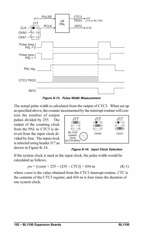
BL1100192 s BL1100 Expansion Boards
Figure K-13. Pulse Width Measurement
The actual pulse width is calculated from the output of CTC3. When set upas specified above, the counter incremented by the interrupt routine will con-tain the number of outputpulses divided by 255. Theoutput of the counting clockfrom the PAL to CTC3 is de-rived from the input clock di-vided by four. The input clockis selected using header J17 asshown in Figure K-14.
If the system clock is used as the input clock, the pulse width would becalculated as follows.
pw = [count × 255 + (255 CTC)] × 434 ns (K-1)
where count is the value obtained from the CTC3 interrupt routine, CTC isthe contents of the CTC3 register, and 434 ns is four times the duration ofone system clock.
/ INT2
CTC3TRG3U6
PAL
PULSEJ6:1
J2:20PCLK
Pulse (neg.)P0L = 0
Pulse (pos.)P0L = 1
PAL reg.
CTC3 TRG3
/INT2
1
3
5
CLKCKA0CKA1
J17
J3:8(J12 on BL1100)
Figure K-14. Input Clock Selection
J17135
246
BL1100systemclock
(9.216 MHz)
J17135
246
CKA0
J17135
246
CKA1FD

BL1100 BL1100 Expansion Boards s 193
ClocksThe clocks from the asynchronous port of the Z180 are based on the baudrate set for the port in its CNTLB register.
Bit 5 specifies the prescaler value. If this bit is zero, the prescaler equals10. If bit 5 is set, the prescaler equals 30. The SS bits (0, 1 and 2) set thedivider value according to Table 4-7.
The clock output to CTC3 is calculated as follows.
clock output = system clock/(prescaler × divider × 4)
where the system clock is 9.216 MHz.
If the clock rate is changed, remember to change the baud rateof the associated port. Do not change the baud rate for CKA0if you are using header J7 of the BL1100 as your Dynamic Cprogramming port. This will cause the BL1100 to lose contactwith Dynamic C.
Another consideration when using these ports is that CKA0 and CKA1 aremultiplexed pins. The CKA0 pin is shared with DREQ0, and CKA1 isshared with TEND0. When the system is reset, these pins are switched toCKA0 and CKA1. CKA0 changes when DMA Channel 0 is programmedfor memory to/from I/O (and memory to/from memory mapped I/O).CKA1 will change only if CKA1D of CNTLA0 is set to 1. Memory-to-memory DMA transfers using the function dmacopy will not affect CKA0.
An application for the pulse width measurement system is a device thatgenerates pulse trains. One such device is the Opto22 A/D Module(AD11), which converts an analog signal value to a serial pulse train. Thefrequency range of the output is from 1920 Hz to 9600 Hz.
Other InformationAn additional digital signal is available on pin 2 (PIN) of Wago connectorJ6. This signal can be read by reading the PAL register (x800) for thatboard and examining the low-order bit:
value = inport( PAL ) && 0x01;
Only ADC boards support a PAL at U6.
CNTLB0 (02H) and CNTLB1 (03H)
7 6 5 4 3 2 1 0
MPBT MP /CTSPS PEO DR SS2 SS1 SS0
R / W R / W R / W R / W R / W R / W R / W R / W
!
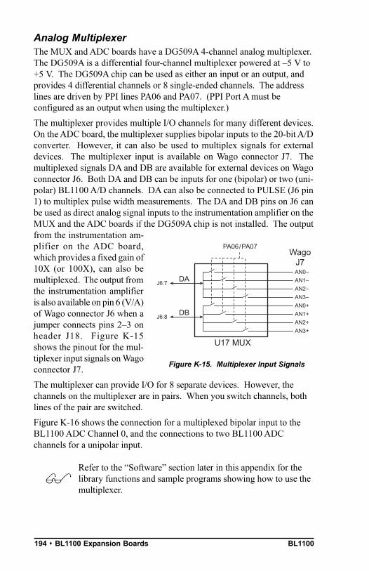
BL1100194 s BL1100 Expansion Boards
Analog MultiplexerThe MUX and ADC boards have a DG509A 4-channel analog multiplexer.The DG509A is a differential four-channel multiplexer powered at 5 V to+5 V. The DG509A chip can be used as either an input or an output, andprovides 4 differential channels or 8 single-ended channels. The addresslines are driven by PPI lines PA06 and PA07. (PPI Port A must beconfigured as an output when using the multiplexer.)
The multiplexer provides multiple I/O channels for many different devices.On the ADC board, the multiplexer supplies bipolar inputs to the 20-bit A/Dconverter. However, it can also be used to multiplex signals for externaldevices. The multiplexer input is available on Wago connector J7. Themultiplexed signals DA and DB are available for external devices on Wagoconnector J6. Both DA and DB can be inputs for one (bipolar) or two (uni-polar) BL1100 A/D channels. DA can also be connected to PULSE (J6 pin1) to multiplex pulse width measurements. The DA and DB pins on J6 canbe used as direct analog signal inputs to the instrumentation amplifier on theMUX and the ADC boards if the DG509A chip is not installed. The outputfrom the instrumentation am-plifier on the ADC board,which provides a fixed gain of10X (or 100X), can also bemultiplexed. The output fromthe instrumentation amplifieris also available on pin 6 (V/A)of Wago connector J6 when ajumper connects pins 23 onheader J18. Figure K-15shows the pinout for the mul-tiplexer input signals on Wagoconnector J7.
The multiplexer can provide I/O for 8 separate devices. However, thechannels on the multiplexer are in pairs. When you switch channels, bothlines of the pair are switched.
Figure K-16 shows the connection for a multiplexed bipolar input to theBL1100 ADC Channel 0, and the connections to two BL1100 ADCchannels for a unipolar input.
Refer to the Software section later in this appendix for thelibrary functions and sample programs showing how to use themultiplexer.
DAJ6:7
AN0
DBJ6:8
AN0+
AN1
AN1+
AN2
AN2+
AN3
AN3+
PA06/PA07
U17 MUX
WagoJ7
Figure K-15. Multiplexer Input Signals
$

BL1100 BL1100 Expansion Boards s 195
Figure K-16. Connecting Multiplexed Bipolar and Unipolar Inputs to BL1100
Instrumentation AmplifierThe MUX and ADC boards include an instrumentation amplifier (LT1101at U7) that has a high input resistance, high linearity (8 ppm), and lowoffset voltage drift (0.4 µV/°C). The LT1101 has a pair of differential inputsfrom the analog multiplexer, and is used with the multiplexer for signalconditioning for the A/D converter or for other off-board devices. Asecondary op amp, U8, conditions the amplifiers output.
The LT1101 has a fixed gain of 10 when its pins 1 and 2 and pins 7 and 8 areconnected. A fixed gain of 100 is attainable by cutting the printed circuitboard traces between pins 1 and 2 and between pins 7 and 8.
Figure K-17 shows the instrumentation amplifier, and where to cut thecircuit board trace to realize a gain of 100.
The output from the instrumentation amplifier can be multiplexed. Theoutput is also available on pin 6 (V/A) of header J6 when the jumper on headerJ18 connects pins 23.
AN0AN0+AN1AN1+AN2AN2+AN3AN3+
DADB
CH0LCH0H
ExpansionBoard
AN0AN0+AN1AN1+AN2AN2+AN3AN3+
DADB
CH0LCH0H
ExpansionBoard
CH1LCH1H
BL1100
BL1100
U17MUX ADC
U17MUX ADC
WagoJ7
WagoJ6
WagoJ4
WagoJ7
WagoJ6
WagoJ4
Bipolar Input to BL1100
Unipolar Input to BL1100

BL1100196 s BL1100 Expansion Boards
Figure K-17. Instrumentation Amplifier I/O and Gain
A/D ConverterThe ADC board includes a high-resolution 20-bit A/D converter (AD7701at U3) for measuring low-frequency analog signals. The AD7701 has avery high resolution (1 bit = 2.384 µV for a voltage input range of 0 V to2.5 V) with 0.0003% accuracy, and allows either bipolar or unipolarmeasurements. There are three internal calibration modes. An indepen-dent voltage measurement can be taken every 125 ms. Two-stage signalconditioning uses the instrumentation amplifier as the first stage ofamplification, followed by a second op-amp whose gain is adjustable.
Port A of the programmable peripheral interface (PPI) and lines 0 and 1 ofthe buffered TTL input must be used in conjunction with the A/D con-verter. These I/O lines are not available for normal use when the A/Dconvertre is using them. The other PPI ports and lines 27 of the TTLinput remain available for your application. Figure K-18 shows theseinterfaces to the A/D converter.
Figure K-18. A/D Convertre Interfacewith PPI and TTL Buffer
+
DA
DB
AOUTU7
U7Solder side
Cut herefor gainof 100
Cut herefor gainof 100
PA00
AIN
PA01PA02PA03PA04PA05
IN0IN1
PPI
TTL
BPCAL/CSSC2SCLKSC1
SDAT/DRDY
REF +2.5 V
U320-bit ADC
AD7703
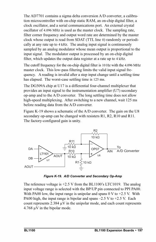
BL1100 BL1100 Expansion Boards s 197
The AD7701 contains a sigma delta conversion A/D converter, a calibra-tion microcontroller with on-chip static RAM, an on-chip digital filter, aclock oscillator, and a serial communications port. An external crystaloscillator of 4.096 MHz is used as the master clock. The sampling rate,filter corner frequency and output word rate are determined by the masterclock whose output is read from SDAT (TTL line 0) randomly or periodi-cally at any rate up to 4 kHz. The analog input signal is continuouslysampled by an analog modulator whose mean output is proportional to theinput signal. The modulator output is processed by an on-chip digitalfilter, which updates the output data register at a rate up to 4 kHz.
The cutoff frequency for the on-chip digital filter is 10 Hz with the 4.096 MHzmaster clock. This low-pass filtering limits the valid input signal fre-quency. A reading is invalid after a step input change until a settling timehas elapsed. The worst-case settling time is 125 ms.
The DG509A chip at U17 is a differential four-channel multiplexer thatprovides an input signal to the instrumentation amplifier (U7) secondaryop-amp and to the A/D converter. The long settling time does not allowhigh-speed multiplexing. After switching to a new channel, wait 125 msbefore reading data from the A/D converter.
Figure K-19 shows a schematic of the A/D converter. The gain on the U8secondary op-amp can be changed with resisters R1, R2, R10 and R11.The factory-configured gain is unity.
Figure K-19. A/D Converter and Secondary Op-Amp
The reference voltage is +2.5 V from the BL1100s LTC1019. The analoginput voltage range is selected with the BP/UP pin connected to PPI PA00.With PA00 low, the input range is unipolar and spans 0 V to +2.5 V. WithPA00 high, the input range is bipolar and spans 2.5 V to +2.5 V. Eachcount represents 2.384 µV in the unipolar mode, and each count represents4.768 µV in the bipolar mode.
+
DA
DBAOUT
LT1101+
OP07
U7
U8
AOUT
AIN
R2
R11
R10
R1
10 kΩ
10 kΩ
10 kΩ
10 kΩ
ToA/D Converter

BL1100198 s BL1100 Expansion Boards
The output coding format looks like this.
Unipolar Bipolar Output Data
+2.5 V +2.5 V 1111 1111 1111 1111 1111 1111+1.25 V 0.0 V 1000 0000 0000 0000 0000 0000
0.0 V 2.5 V 0000 0000 0000 0000 0000 0000
The AD7701 offers both self- and system calibration using an on-chipcalibration controller and SRAM. The calibration mode pin, CAL, is con-nected to PA01. When CAL is taken high for more than four cycles of themaster clock, the A/D converter is reset and performs a calibration cyclewhen CAL is brought low again. The calibration control inputs SC1 andSC2 are connected to PA05 and PA03. Table K-3 lists the calibration options.
In the self-calibration mode, the zero scale is calibrated against the AGNDpin and the full scale is calibrated against the VREF pin to remove internalerrors. System calibration uses voltage values presented by the system tothe AIN pin for the zero and full-scale points to compensate for systemgain and offset errors.
There are two system-calibration modes. The two-step system calibrationmode calibrates both the system offset and the system gain. The one-stepcalibration mode uses an input voltage as the system zero-scale calibrationpoint, but uses the VREF value as the full-scale point.
Any drift in the temperature input offset is minimized by chopper stabiliz-ation techniques. The drift arising from temperature changes is relativelyflat at temperatures from 0 °C to 70°C, with less than 10 LSB. Above75°C, the offset drift doubles approximately every 10°C.
Gain drift is significantly less than offset drift. The typical gain drift is lessthan 40 LSB over the specified temperature range.
Using system calibration can minimize offset and gain errors in the signalconditioning circuit, multiplexer, and sensor. Measurement errors attribut-ed to offset drift or gain drift can be eliminated at any time by recalibratingthe system.
Table K-3. AD7703 Calibration Options
CalibrationType SC1 SC2 Zero Full Scale Steps
Self calibration 0 0 AGND VREF 1
System offset 1 1 AIN 1 of 2
System gain 0 1 AIN 2 of 2
System offset 1 0 AIN VREF 1
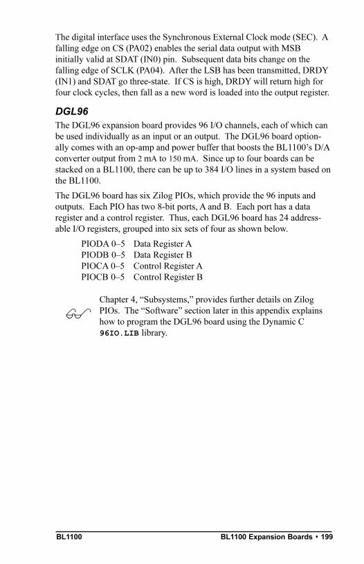
BL1100 BL1100 Expansion Boards s 199
The digital interface uses the Synchronous External Clock mode (SEC). Afalling edge on CS (PA02) enables the serial data output with MSBinitially valid at SDAT (IN0) pin. Subsequent data bits change on thefalling edge of SCLK (PA04). After the LSB has been transmitted, DRDY(IN1) and SDAT go three-state. If CS is high, DRDY will return high forfour clock cycles, then fall as a new word is loaded into the output register.
DGL96The DGL96 expansion board provides 96 I/O channels, each of which canbe used individually as an input or an output. The DGL96 board option-ally comes with an op-amp and power buffer that boosts the BL1100s D/Aconverter output from 2 mA to 150 mA. Since up to four boards can bestacked on a BL1100, there can be up to 384 I/O lines in a system based onthe BL1100.
The DGL96 board has six Zilog PIOs, which provide the 96 inputs andoutputs. Each PIO has two 8-bit ports, A and B. Each port has a dataregister and a control register. Thus, each DGL96 board has 24 address-able I/O registers, grouped into six sets of four as shown below.
PIODA 05 Data Register APIODB 05 Data Register BPIOCA 05 Control Register APIOCB 05 Control Register B
Chapter 4, Subsystems, provides further details on ZilogPIOs. The Software section later in this appendix explainshow to program the DGL96 board using the Dynamic C96IO.LIB library.
$
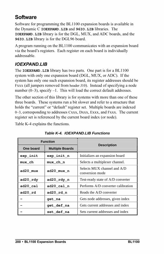
BL1100200 s BL1100 Expansion Boards
SoftwareSoftware for programming the BL1100 expansion boards is available inthe Dynamic C IOEXPAND.LIB and 96IO.LIB libraries. TheIOEXPAND.LIB library is for the DGL, MUX, and ADC boards, and the96IO.LIB library is for the DGL96 board.
A program running on the BL1100 communicates with an expansion boardvia the boards registers. Each register on each board is individuallyaddressable.
IOEXPAND.LIBThe IOEXPAND.LIB library has two parts. One part is for a BL1100system with only one expansion board (DGL, MUX, or ADC). If thesystem has only one such expansion board, its register addresses should beFxxx (all jumpers removed from header J10). Instead of specifying a nodenumber (03), specify 1. This will load the correct default addresses.
The other section of this library is for systems with more than one of thesethree boards. These systems run a bit slower and refer to a structure thatholds the current or default register set. Multiple boards are indexed03, corresponding to addresses Cxxx, Dxxx, Exxx, and Fxxx. The currentregister set is referenced by the current board index (or node).
Table K-4 explains the functions.
Table K-4. IOEXPAND.LIB Functions
Function
One board Multiple BoardsDescription
exp_init exp_init_n Initializes an expansion board
mux_ch mux_ch_n Selects a multiplexer channel.
ad20_mux ad20_mux_nSelects MUX channel and A/Dconversion mode
ad20_rdy ad20_rdy_n Test-ready state of A/D converter
ad20_cal ad20_cal_n Performs A/D converter calibration
ad20_rd ad20_rd_n Reads the A/D converter
— get_na Gets node addresses, given index
— get_def_na Gets current addresses and index
— set_def_na Sets current addresses and index

BL1100 BL1100 Expansion Boards s 201
To use an analog multiplexer or an ADC, first initialize PPI Port A of theboard to be an output. Use the exp_init or exp_init_n function.
int exp_init( int a, int b, int c1, int c2 )
Initializes the programmable peripheral interface (PPI) for Mode 0.This function affects only I/O expansion boards with the default baseaddress of Fxxx. The function sets up the correct control word for theconfiguration of the ports and immediately sets all output lines to thevalue of the given port parameter.
PARAMETERS: a, b, c1, and c2 are output values for the PPI outputregister. Pass a = 1 to configure Port A as an input. Pass b = 1 toconfigure Port B as an input. Pass c1 = 1 to configures Port C uppernibble as inputs. Pass c2 = 1 to configures Port C lower nibble asinputs. All PPI output ports are reset to low when the mode is changed.
Output a correct value to the output port right after the mode ischanged.
Use any other value to specify a port as output. The parameters valueis written to the port after the mode is changed.
After initializing the ports, they can be read or written with the inportand outport functions. Each bit position represents one line of theport, with a 1 indicating that the level is high and a 0 indicating that thelevel is low.
The sample program IOE_DGL.C shows how the initialize and read PPIports.
int exp_init_n( int node, int a, int b, int c1,int c2, int def )
Initializes the expansion board specified by node. The function sets upthe correct control word for the configuration of the ports and immedi-ately sets all output lines to the values of the given parameters.
PARAMETERS: node is the base address for the expansion board toinitialize. Use the values 03 for specific base addresses. Use 1 forthe default node address (see def).
a, b, c1, c2 are port values that specify whether the port is an input oran output. Use 1 to specify a port as input and any other value tospecify a port as output as in exp_init. The parameters value (lowereight bits) is written to the port after the ports mode is changed.
def specifies that the specified node is to be the new default when defis non-zero..
!
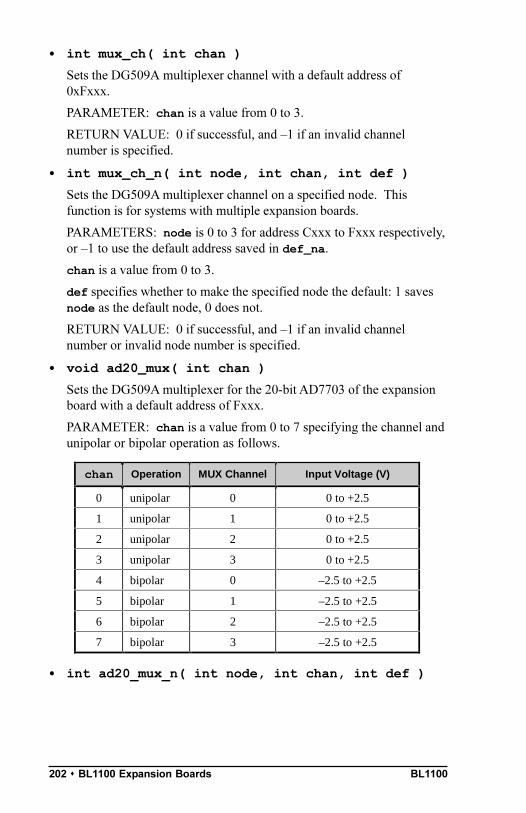
BL1100202 s BL1100 Expansion Boards
int mux_ch( int chan )
Sets the DG509A multiplexer channel with a default address of0xFxxx.
PARAMETER: chan is a value from 0 to 3.
RETURN VALUE: 0 if successful, and 1 if an invalid channelnumber is specified.
int mux_ch_n( int node, int chan, int def )
Sets the DG509A multiplexer channel on a specified node. Thisfunction is for systems with multiple expansion boards.
PARAMETERS: node is 0 to 3 for address Cxxx to Fxxx respectively,or 1 to use the default address saved in def_na.
chan is a value from 0 to 3.
def specifies whether to make the specified node the default: 1 savesnode as the default node, 0 does not.
RETURN VALUE: 0 if successful, and 1 if an invalid channelnumber or invalid node number is specified.
void ad20_mux( int chan )
Sets the DG509A multiplexer for the 20-bit AD7703 of the expansionboard with a default address of Fxxx.
PARAMETER: chan is a value from 0 to 7 specifying the channel andunipolar or bipolar operation as follows.
int ad20_mux_n( int node, int chan, int def )
chan Operation MUX Channel Input Voltage (V)
0 unipolar 0 0 to +2.5
1 unipolar 1 0 to +2.5
2 unipolar 2 0 to +2.5
3 unipolar 3 0 to +2.5
4 bipolar 0 –2.5 to +2.5
5 bipolar 1 –2.5 to +2.5
6 bipolar 2 –2.5 to +2.5
7 bipolar 3 –2.5 to +2.5

BL1100 BL1100 Expansion Boards s 203
Sets the DG509A multiplexer for the 20-bit AD7703 of the expansionboard in a system with multiple expansion boards.
PARAMETERS: node is 0 to 3 for address Cxxx to Fxxx respectively,or 1 to use the default address saved in def_na.
chan is a value from 0 to 7 specifying the channel and unipolar orbipolar operation as described for ad20_mux.
def specifies whether to make the specified node the default: 1 savesnode as the default node, 0 does not.
RETURN VALUE: 0 if successful and 1 if an invalid parameter ispassed.
int ad20_rdy()
Tests AD7703 /DRDY status from RDTTL bit 1.
RETURN VALUE: 1 if the A/D convertre is ready, and 0 if not.
int ad20_rdy_n( int node )
Tests AD7703 /DRDY status from RDTTL bit 1 of a specified node.
PARAMETER: node is 0 to 3 for address Cxxx to Fxxx respectively,or 1 to use the default address saved in def_na.
RETURN VALUE: 0 if the A/D converter on the specified board isready, and 1 if the A/D convertre is busy or if an invalid node ispassed.
int ad20_cal( int mode )
Calibrates the A/D converter of the expansion board with a defaultaddress of Fxxx. The function waits for the A/D converter to becomeready before returning.
PARAMETER: mode can be 0, 1, or 2, as explained below.
Mode 0, self-calibration as described in Table K-3, does not usethe multiplexer.
Mode 1 calibration uses the multiplexer to get zero-scale andfull-scale readings on AIN. MUX ch0 is the A/D signal to bemeasured. MUX ch1 is AIN for the first step, which calibratesthe system offset. MUX ch2 is AIN for the second step, whichcalibrates the system gain.
Mode 2 calibration uses the current channel to get AIN as thezero-scale reading to calibrate the system offset.
RETURN VALUE: 0 if successful, and 1 if an error occured.
int ad20_cal_n( int node, int mode, int def )

BL1100204 s BL1100 Expansion Boards
Calibrates the AD7703 A/D converter on the specified board.
PARAMETER: node is 0 to 3 for address Cxxx to Fxxx respectively,or 1 to use the default address saved in def_na.
mode can be 0, 1, or 2, as explained below.
Mode 0, self-calibration as described in Table K-3, does not usethe multiplexer.
Mode 1 calibration uses the multiplexer to get zero-scale andfull-scale readings on AIN. MUX ch0 is the A/D signal to bemeasured. MUX ch1 is AIN for the first step, which calibratesthe system offset. MUX ch2 is AIN for the second step, whichcalibrates the system gain.
Mode 2 calibration uses the current channel to get AIN as thezero-scale reading to calibrate the system offset.
def specifies whether to make the specified node the default: 1 savesnode as the default node, 0 does not.
RETURN VALUE: 0 if successful, and 1 if an error occured.
long ad20_rd()
Reads 20-bit data from the AD7703 serial data port. The functionwaits for the A/D converter to become ready before reading. It doesthis by sampling TTL line 0 (which represents ADC SDAT) 20 times.
RETURN VALUE: 20-bit data. Unipolar mode: 00000 = AGND,7FFFF = 1.25 V, and FFFFF = 2.5 V; bipolar mode: 00000 = 2.5 V,7FFFF = AGND, and FFFFF = 2.5 V.
Because of the 125 ms step response time of the AD7703, atime delay should be guaranteed after a multiplexer switching.
long ad20_rd_n( int node, int def )
Reads 20-bit data from the AD7703 serial data port. The functionwaits for the A/D converter to become ready before reading.
PARAMETER: node is 0 to 3 for address Cxxx to Fxxx respectively,or 1 to use the default address saved in def_na.
def specifies whether to make the specified node the default: 1 savesnode as the default node, 0 does not.
RETURN VALUE: 20-bit data. Unipolar mode: 00000 = AGND,7FFFF = 1.25 V, and FFFFF = 2.5 V; bipolar mode: 00000 = 2.5 V,7FFFF = AGND, and FFFFF = 2.5 V. Returns 1 for an invalid node.
Because of the 125 ms step response time of the AD7703, atime delay should be guaranteed after a multiplexer switching.
!
BL1100 BL1100 Expansion Boards s 205
int get_na( int node, struct node_addr *na )
Gets the corresponding node address from the specified node. Loadsthe structure to which na points with the correct addresses for the nodespecified.
PARAMETER: node is 0 to 3 for address Cxxx to Fxxx respectively.
RETURN VALUE: 0 if the node is proper, 1 if the node is out ofrange.
int set_def_na( int node )
Sets the default node address.
RETURN VALUE: Data from get_na, 1 if an invalid node numberis specified.
int get_def_na( struct node_addr *na )
Loads the default node address into the structure to which na points.
RETURN VALUE: default node number.
96IO.LIBThis library includes several parameters, a number of functions to control,read and write from/to the PIO ports, and an error-trapping facility.
void Init_Board_0()
Sets all bits on board address 0 to inputs.
void Set_Port_Dir( int board, int pio_num,int port, char mask )
Sets the bit directions for the specified port of the specified PIO on thespecified board.
PARAMETERS: board specifies which board to address: 08x00,19x00, 2Ax00, 3Bx00.
pio_num specifies PIO 05.
port specifies the PIO port: 0Port A, 1Port B.
mask is the bit mask for the port: Bit Set = input bit (1), Bit Clear =output bit (0s).
void Set_Bit_Dir( int board, int pio_num,int port, int bit_num, int dir )
$
BL1100206 s BL1100 Expansion Boards
Sets the direction of an individual bit of the specified PIO port on thespecified board.
PARAMETERS: board specifies which board to address: 08x00,19x00, 2Ax00, 3Bx00.
pio_num specifies PIO 05.
port specifies the PIO port of a PIO: 0Port A, 1Port B.
bit_num specifies the bit in the port (07).
dir may be input (1) or output (0). Any other value for dir producesan error.
int Port_Addr( int board, int pio_num,int register )
Returns the address of a PIO register on the specified board. An errorresults if any of the parameters is out of range.
PARAMETERS: board specifies which board to address: 08x00,19x00, 2Ax00, 3Bx00.
pio_num specifies PIO 05.
register must be DA (0), DB (1), CA (2), or CB (3).
RETURN VALUE: Address of PIO register
void Set_PIO_Board( int board, int dir )
Sets all PIOs on the specified board to Mode 3: all input or alloutput.
PARAMETERS: board specifies which board to address: 08x00,19x00, 2Ax00, 3Bx00.
dir may be input (1) or output (0). Any other value for dir producesan error.
void Write_Port( int board, int pio_num,int port, byte value )
Writes value to the specified port of the specified PIO on the speci-fied board.
PARAMETERS: board specifies which board to address: 08x00,19x00, 2Ax00, 3Bx00.
pio_num specifies PIO 05.
port specifies the PIO port of a PIO: 0Port A, 1Port B.
char Read_Port( int board, int pio_num,int port, int mode )

BL1100 BL1100 Expansion Boards 207
• char Read_Port( int board, int pio_num,int port, int mode )
Reads the value of the specified port of the specified PIO on thespecified board. The function reads only the input bits of the port.PARAMETERS: board specifies which board to address: 0—8x00,1—9x00, 2—Ax00, 3—Bx00.pio_num specifies PIO 0–5.port specifies the PIO port of a PIO: 0—Port A, 1—Port B.mode determines the output bits: 1 if mode = FILL_MODE, 0 if mode =STRIP_MODE.RETURN VALUE: The value read. The output bits of the returnedvalue are set to 1 if mode is FILL_MODE, and are set to 0 of mode isSTRIP_MODE. An error results if port or mode is not as specified.
Sample ProgramsPulse Width MeasurementThe following sample program program, PWM.C from the Dynamic CSAMPLES\IOE directory, illustrates how to set up and perform a pulsewidth measurement.
PWM.C
/* Use PAL FP04100.PDS for pulse width measurement. Pulse input is at Wago J6, line 1. Counting clock (from J17) is CKA0. PAL FP04100 divides counting clock by 4. For system clock of 9.216MHz, each count is 0.434 µs. Count clock is sent to CTC3 TRG3. POL = 0: measure Negative Pulse. PAL = 0: disabled POL = 1: measure Positive Pulse. PAL = 1: enabled Writing 0xC5 (1100 0101) to CTC3 has these effects: ^^ ^ ^ || | |- this is a control word || |- time constant follows (it’s 255) ||- counter mode, not timer mode |- enable interrupt */ int i, l, m; // temporaries unsigned int n; // pulse width char flag; // set when pulse ends char count; // count full CTC cycles
continued…

BL1100208 BL1100 Expansion Boards
main() outport(CTC0,CTC3_VEC); // set interrupt vector
outport(PAL,0); // disable PAL outport(POL,0); // negative pulses while(1) count = 0;
flag = 0; outport(CTC3,0x03); // software reset outport(CTC3,0xC5); // see note above outport(CTC3,0xFF); // 255 ISET(ITC,2); // enable INT2 outport(PAL,1); // enable PAL while(!flag) m = inport(CTC3); width = count * 255 + (255 - m);
++l; printf("Count = %d. Width = %u %d\n", count, width, l);
for(i=0; i<10000; ++i) // wait #INT_VEC CTC3_VEC ctc3int #asm nodebug ctc3int:: // increments count
push af ld a,(count) inc a ld (count),a pop af ei reti
#endasm #INT_VEC INT2_VEC int2int interrupt ret int2int()
outport(PAL,0); // disable PAL IRES(ITC,2); // turn off INT2 flag = 1;
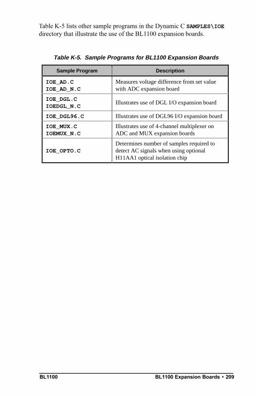
BL1100 BL1100 Expansion Boards s 209
Table K-5 lists other sample programs in the Dynamic C SAMPLES\IOEdirectory that illustrate the use of the BL1100 expansion boards.
Table K-5. Sample Programs for BL1100 Expansion Boards
Sample Program Description
IOE_AD.CIOE_AD_N.C
Measures voltage difference from set valuewith ADC expansion board
IOE_DGL.CIOEDGL_N.C
Illustrates use of DGL I/O expansion board
IOE_DGL96.C Illustrates use of DGL96 I/O expansion board
IOE_MUX.CIOEMUX_N.C
Illustrates use of 4-channel multiplexer onADC and MUX expansion boards
IOE_OPTO.CDetermines number of samples required todetect AC signals when using optionalH11AA1 optical isolation chip
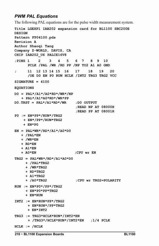
BL1100210 s BL1100 Expansion Boards
PWM PAL EquationsThe following PAL equations are for the pulse width measurement system.
Title LGEXP1 IAB202 expansion card for BL1100 SBC200EDESIGNPattern FP04100.pdsRevision AAuthor Shaoqi TangCompany Z-WORLD, DAVIS, CACHIP IAB202_U6 PALCE16V8
;PINS 1 2 3 4 5 6 7 8 9 10 PCLK /PAL /WR /RD PP /NP TO2 A1 A0 GND
; 11 12 13 14 15 16 17 18 19 20 /OE D0 EN P0 RUN HCLK /INT2 TRG3 TRG2 VCC
SIGNATURE = 4100
EQUATIONS
D0 = PAL*/A1*/A0*RD*/WR*/NP + PAL*/A1*A0*RD*/WR*PPD0.TRST = PAL*/A1*RD*/WR ;D0 OUTPUT ;READ NP AT 08000H ;READ PP AT 08001HP0 := EN*PP*/RUN*/TRG2 + EN*/PP*/RUN*TRG2 + EN*P0
EN = PAL*WR*/RD*/A1*/A0*D0 + /PAL*EN + /WR*EN + RD*EN + A1*EN + A0*EN ;CPU wr EN
TRG2 = PAL*WR*/RD*/A1*A0*D0 + /PAL*TRG2 + /WR*TRG2 + RD*TRG2 + A1*TRG2 + /A0*TRG2 ;CPU wr TRG2=POLARITY
RUN := EN*P0*/PP*/TRG2 + EN*P0*PP*TRG2 + EN*RUN
INT2 := EN*RUN*PP*/TRG2 + EN*RUN*/PP*TRG2 + EN*INT2
TRG3 := TRG3*HCLK*RUN*/INT2*EN + /TRG3*/HCLK*RUN*/INT2*EN ;1/4 PCLK
HCLK := /HCLK
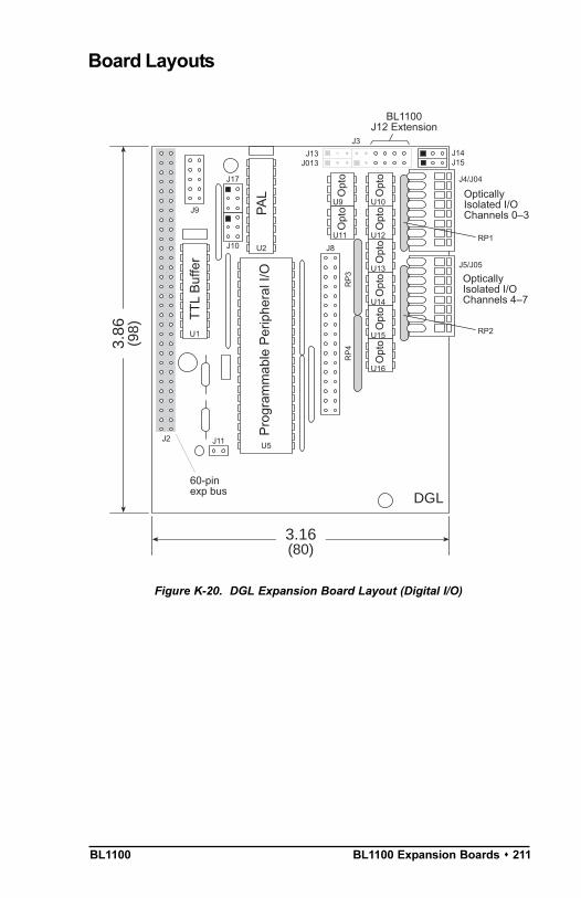
BL1100 BL1100 Expansion Boards s 211
Board Layouts
Figure K-20. DGL Expansion Board Layout (Digital I/O)
Opt
o
PA
L
TT
L B
uffe
r
U2
U1
U9 U10
U11 U12
Opt
o
Opt
o
Opt
oO
pto
Opt
oO
pto
Opt
o
U13
U14
U15
U16
J14J15
BL1100J12 Extension
J4/J04
J5/J05P
rogr
amm
able
Per
iphe
ral I
/O
U5J2 J11
J9
J17
J10 J8
RP
4R
P3
RP2
RP1
J3
J13J013
60-pinexp bus
OpticallyIsolated I/OChannels 03
OpticallyIsolated I/OChannels 47
DGL
3.86
(98)
3.16(80)

BL1100212 s BL1100 Expansion Boards
Figure K-21. MUX Expansion Board Layout (Multiplexer)
PA
LU2
BL1100J12 Extension
Multiplexer I/O
MultiplexedChannels 03,Analog Input
J6/J06
J7/J07
U17
Mul
tiple
xer
U7
Pro
gram
mab
le P
erip
hera
l I/O
U5J2 J11
J17
J10 J8
RP
4R
P3
J18
J3J13
J013
60-pinexp bus
1×16headerfor PPIports C1and C2
InstrumentationAmplifier MUX
3.86
(98)
3.16(80)
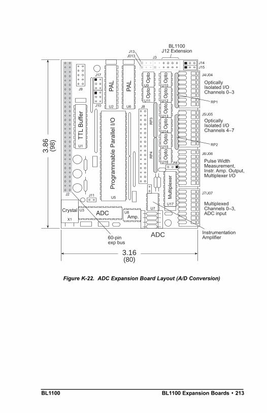
BL1100 BL1100 Expansion Boards s 213
Figure K-22. ADC Expansion Board Layout (A/D Conversion)
Opt
o
PA
L
PA
L
TT
L B
uffe
r
U2 U6
U1
U9 U10
U11 U12
Opt
o
Opt
o
Opt
oO
pto
Opt
oO
pto
Opt
o
U13
U14
U15
U16
J14J15
BL1100J12 Extension
J4/J04
J5/J05
Pulse WidthMeasurement,Instr. Amp. Output,Multiplexer I/O
MultiplexedChannels 03,ADC input
J6/J06
J7/J07
U17
U8U3
Mul
tiple
xer
Amp.
U7
ADC
Pro
gram
mab
le P
aral
lel I
/O
U5
X1
Crystal
J2 J11
J9
J17
J10 J8
RP
4R
P3
RP2
RP1
J18
J3
J13J013
60-pinexp bus
InstrumentationAmplifier
OpticallyIsolated I/OChannels 47
OpticallyIsolated I/OChannels 03
ADC
3.86
(98)
3.16(80)
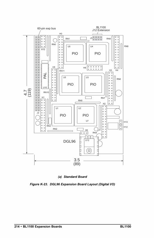
BL1100214 s BL1100 Expansion Boards
(a) Standard Board
Figure K-23. DGL96 Expansion Board Layout (Digital I/O)
PA
L
U10
BL1100J12 Extension
U7
J2
H10
PIO
U0
PIO
U4
PIO
U5
PIO
U3
PIO
U1
PIO
U2
H1
H2
H6
H5
H0
H4H3
H13
H12
RN0
RN1 RN9
RN8
H8
RN7
RN6
RN11
RN10
RN5
RN4
RN2RN3
J3
60-pin exp bus
U12DGL96
4.7
(119
)
3.5(89)
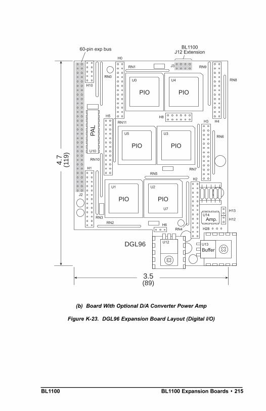
BL1100 BL1100 Expansion Boards s 215
(b) Board With Optional D/A Converter Power Amp
Figure K-23. DGL96 Expansion Board Layout (Digital I/O)
PA
L
U10
BL1100J12 Extension
U14Amp.
U7
J2
H10
PIO
U0
PIO
U4
PIO
U5
PIO
U3
PIO
U1
PIO
U2
H1
H2
H6H28
H5
H0
H4H3
H13
H12
RN0
RN1 RN9
RN8
H8
RN7
RN6
RN11
RN10
RN5
RN4
RN2RN3
J3
60-pin exp bus
U12 U13
BufferDGL96
4.7
(119
)
3.5(89)
BL1100216 s BL1100 Expansion Boards
I/O MapThe different registers in the I/O space can be accessed in Dynamic Cusing the register addresses in Tables K-6 and K-7. The library functionsinport and outport access the I/O registers directly.
data_value = inport (PAL_C);
outport (PAL_C, data_value);
The library functions IBIT, ISET, and IRES allow bits in the I/O registersto be tested, set, and cleared respectively..
Both 16-bit and 8-bit I/O addresses can be used. Up to four I/O expansionboards can be stacked.
Table K-6 lists the register addresses for the DGL, MUX, and ADCexpansion boards. The default base address is Fxxx, so the symbolicnames do not include the base address specifier.
Table K-7 lists the register addresses for the DGL96 expansion board.Each PIO on each board has four registers.

BL1100 BL1100 Expansion Boards s 217
Table K-6. DGL, MUX, and ADC Expansion Board Registers
Address Name Description
C400 RDTTL_C Buffered TTL-level input
C800 PAL_C Pulse width measurement PAL
C801 POL_C Polarity for PWM
CC00 PPIA_C Port A, PPI
CC01 PPIB_C Port B, PPI
CC02 PPIC_C Port C, PPI
CC03 PPICN_C PPI control register
D400 RDTTL_D Buffered TTL-level input
D800 PAL_D Pulse width measurement PAL
D801 POL_D Polarity for PWM
DC00 PPIA_D Port A, PPI
DC01 PPIB_D Port B, PPI
DC02 PPIC_D Port C, PPI
DC03 PPICN_D PPI control register
E400 RDTTL_E Buffered TTL-level input
E800 PAL_E Pulse width measurement PAL
E801 POL_E Polarity for PWM
EC00 PPIA_E Port A, PPI
EC01 PPIB_E Port B, PPI
EC02 PPIC_E Port C, PPI
EC03 PPICN_E PPI control register
F400 RDTTL Buffered TTL-level input
F800 PAL Pulse width measurement PAL
F801 POL Polarity for PWM
FC00 PPIA Port A, PPI
FC01 PPIB Port B, PPI
FC02 PPIC Port C, PPI
FC03 PPICN PPI control register

BL1100218 s BL1100 Expansion Boards
Table K-7. DGL96 Expansion Board Registers
Address Description Address Description
8000 PIO 0, data, Port A 8002 PIO 0, control, Port A
8001 PIO 0, data, Port B 8003 PIO 0, control, Port B
8200 PIO 1, data, Port A 8202 PIO 1, control, Port A
8201 PIO 1, data, Port B 8203 PIO 1, control, Port B
8400 PIO 2, data, Port A 8402 PIO 2, control, Port A
8401 PIO 2, data, Port B 8403 PIO 2, control, Port B
8600 PIO 3, data, Port A 8602 PIO 3, control, Port A
8601 PIO 3, data, Port B 8603 PIO 3, control, Port B
8800 PIO 4, data, Port A 8802 PIO 4, control, Port A
8801 PIO 4, data, Port B 8803 PIO 4, control, Port B
8A00 PIO 5, data, Port A 8A02 PIO 5, control, Port A
8A01 PIO 5, data, Port B 8A03 PIO 5, control, Port B
9000 PIO 0, data, Port A 9002 PIO 0, control, Port A
9001 PIO 0, data, Port B 9003 PIO 0, control, Port B
9200 PIO 1, data, Port A 9202 PIO 1, control, Port A
9201 PIO 1, data, Port B 9203 PIO 1, control, Port B
9400 PIO 2, data, Port A 9402 PIO 2, control, Port A
9401 PIO 2, data, Port B 9403 PIO 2, control, Port B
9600 PIO 3, data, Port A 9602 PIO 3, control, Port A
9601 PIO 3, data, Port B 9603 PIO 3, control, Port B
9800 PIO 4, data, Port A 9802 PIO 4, control, Port A
9801 PIO 4, data, Port B 9803 PIO 4, control, Port B
9A00 PIO 5, data, Port A 9A02 PIO 5, control, Port A
9A01 PIO 5, data, Port B 9A03 PIO 5, control, Port B
A000 PIO 0, data, Port A A002 PIO 0, control, Port A
A001 PIO 0, data, Port B A003 PIO 0, control, Port B
A200 PIO 1, data, Port A A202 PIO 1, control, Port A
A201 PIO 1, data, Port B A203 PIO 1, control, Port B
A400 PIO 2, data, Port A A402 PIO 2, control, Port A
A401 PIO 2, data, Port B A403 PIO 2, control, Port B
continued…

BL1100 BL1100 Expansion Boards s 219
Table K-7. DGL96 Expansion Board Registers (concluded)
Address Description Address Description
A600 PIO 3, data, Port A A602 PIO 3, control, Port A
A601 PIO 3, data, Port B A603 PIO 3, control, Port B
A800 PIO 4, data, Port A A802 PIO 4, control, Port A
A801 PIO 4, data, Port B A803 PIO 4, control, Port B
AA00 PIO 5, data, Port A AA02 PIO 5, control, Port A
AA01 PIO 5, data, Port B AA03 PIO 5, control, Port B
B000 PIO 0, data, Port A B002 PIO 0, control, Port A
B001 PIO 0, data, Port B B003 PIO 0, control, Port B
B200 PIO 1, data, Port A B202 PIO 1, control, Port A
B201 PIO 1, data, Port B B203 PIO 1, control, Port B
B400 PIO 2, data, Port A B402 PIO 2, control, Port A
B401 PIO 2, data, Port B B403 PIO 2, control, Port B
B600 PIO 3, data, Port A B602 PIO 3, control, Port A
B601 PIO 3, data, Port B B603 PIO 3, control, Port B
B800 PIO 4, data, Port A B802 PIO 4, control, Port A
B801 PIO 4, data, Port B B803 PIO 4, control, Port B
BA00 PIO 5, data, Port A BA02 PIO 5, control, Port A
BA01 PIO 5, data, Port B BA03 PIO 5, control, Port B

BL1100220 s BL1100 Expansion Boards
Jumper and Header SpecificationsTable K-8 describes all the BL1100 expansion board headers that carrysignals.
ADC, DGL, and MUX Expansion Board SignalsFigure K-24 shows the pinouts for Wago connectors J4/J04J7/J07.
Figure K-24. Pinouts for Wago Connectors
Figure K-25 shows the pinouts for headers J8 and J9.
Table K-8. BL1100 Expansion Board Headers
Expansion BoardHeader Description
DGL96 ADC DGL MUX
H0–H5 PIO Signals á
H28 Power amp connection to BL1100DAC at BL1100 header J28
á
J2 60-pin connector to BL1100 header J24 á á á á
J3 8-pin connector to BL1100 header J12 á á á á
J4/J04 Optically isolated I/O á á
J5/J05 Optically isolated I/O á á
J6/J06 PWM and multiplexer signals á á
J7/J07 Multiplexed analog channels 0–3 á á
J8 PPI Ports A and B á á
J9 TTL Input á á
1
OP
3BO
P3A
OP
2BO
P2A
OP
1BO
P1A
OP
0BO
P0A
J4/J04
OP
7BO
P7A
OP
6BO
P6A
OP
5BO
P5A
OP
4BO
P4A
J5/J05
DB
DA
V/A
AG
ND
GN
DG
ND
PIN
PU
LSE
J6/J06
AN
3+A
N3
AN
2+A
N2
AN
1+A
N1
AN
0+A
N0
J7/J07
NOTEDo not mix analog grounds (J6/J06:5) withdigital grounds (J6/J06:3-4).
ADCDGL
ADCDGL
ADCMUX
ADCMUX
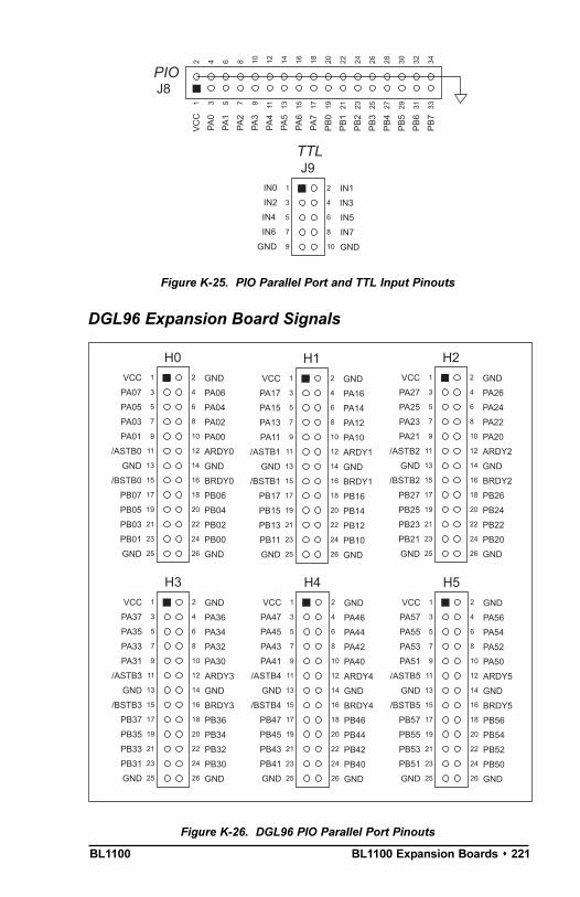
BL1100 BL1100 Expansion Boards s 221
Figure K-25. PIO Parallel Port and TTL Input Pinouts
DGL96 Expansion Board Signals
Figure K-26. DGL96 PIO Parallel Port Pinouts
H01
3
5
7
9
11
13
15
17
19
21
23
25
2
4
6
8
10
12
14
16
18
20
22
24
26
VCC
PA07
PA05
PA03
PA01
/ASTB0
GND
/BSTB0
PB07
PB05
PB03
PB01
GND
GND
PA06
PA04
PA02
PA00
ARDY0
GND
BRDY0
PB06
PB04
PB02
PB00
GND
H11
3
5
7
9
11
13
15
17
19
21
23
25
2
4
6
8
10
12
14
16
18
20
22
24
26
VCC
PA17
PA15
PA13
PA11
/ASTB1
GND
/BSTB1
PB17
PB15
PB13
PB11
GND
GND
PA16
PA14
PA12
PA10
ARDY1
GND
BRDY1
PB16
PB14
PB12
PB10
GND
H21
3
5
7
9
11
13
15
17
19
21
23
25
2
4
6
8
10
12
14
16
18
20
22
24
26
VCC
PA27
PA25
PA23
PA21
/ASTB2
GND
/BSTB2
PB27
PB25
PB23
PB21
GND
GND
PA26
PA24
PA22
PA20
ARDY2
GND
BRDY2
PB26
PB24
PB22
PB20
GND
H31
3
5
7
9
11
13
15
17
19
21
23
25
2
4
6
8
10
12
14
16
18
20
22
24
26
VCC
PA37
PA35
PA33
PA31
/ASTB3
GND
/BSTB3
PB37
PB35
PB33
PB31
GND
GND
PA36
PA34
PA32
PA30
ARDY3
GND
BRDY3
PB36
PB34
PB32
PB30
GND
H41
3
5
7
9
11
13
15
17
19
21
23
25
2
4
6
8
10
12
14
16
18
20
22
24
26
VCC
PA47
PA45
PA43
PA41
/ASTB4
GND
/BSTB4
PB47
PB45
PB43
PB41
GND
GND
PA46
PA44
PA42
PA40
ARDY4
GND
BRDY4
PB46
PB44
PB42
PB40
GND
H51
3
5
7
9
11
13
15
17
19
21
23
25
2
4
6
8
10
12
14
16
18
20
22
24
26
VCC
PA57
PA55
PA53
PA51
/ASTB5
GND
/BSTB5
PB57
PB55
PB53
PB51
GND
GND
PA56
PA54
PA52
PA50
ARDY5
GND
BRDY5
PB56
PB54
PB52
PB50
GND
IN2
IN4
IN6
IN0
J91
3
5
7
9
2
4
6
8
10GND
IN3
IN5
IN7
IN1
GND
TTL
PA
0
PA
1
PA
2
PA
3
PA
4
PA
5
PA
6
PA
7
PB
0
PB
1
PB
2
PB
3
PB
4
PB
5
PB
6
PB
7
VC
C
J8
1 3 5 7 9 11 13 15 17 19 21 23 25 27 29 31 33
2 4 6 8 10 12 14 16 18 20 22 24 26 28 30 32 34
PIO
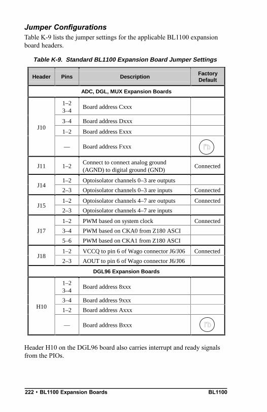
BL1100222 s BL1100 Expansion Boards
Jumper ConfigurationsTable K-9 lists the jumper settings for the applicable BL1100 expansionboard headers.
Header H10 on the DGL96 board also carries interrupt and ready signalsfrom the PIOs.
Table K-9. Standard BL1100 Expansion Board Jumper Settings
Header Pins DescriptionFactoryDefault
ADC, DGL, MUX Expansion Boards
1–23–4
Board address Cxxx
3–4 Board address Dxxx
1–2 Board address ExxxJ10
— Board address Fxxx
J11 1–2Connect to connect analog ground(AGND) to digital ground (GND)
Connected
1–2 Optoisolator channels 0–3 are outputsJ14
2–3 Optoisolator channels 0–3 are inputs Connected
1–2 Optoisolator channels 4–7 are outputs ConnectedJ15
2–3 Optoisolator channels 4–7 are inputs
1–2 PWM based on system clock Connected
3–4 PWM based on CKA0 from Z180 ASCIJ17
5–6 PWM based on CKA1 from Z180 ASCI
1–2 VCCQ to pin 6 of Wago connector J6/J06 ConnectedJ18
2–3 AOUT to pin 6 of Wago connector J6/J06
DGL96 Expansion Boards
1–23–4
Board address 8xxx
3–4 Board address 9xxx
1–2 Board address AxxxH10
— Board address Bxxx
FD
FD

BL1100 Backup Battery 223
APPENDIX L: BACKUP BATTERY

BL1100224 s Backup Battery
Battery Life and Storage ConditionsThe battery on the BL1100 will provide at least 9,000 hours of backuptime for the onboard real-time clock and SRAM. However, backup timelongevity is affected by many factors, including the amount of time thecontroller is unpowered and the SRAM size. Most systems are operatedon a continuous basis, with the battery supplying power to the real-timeclock and the SRAM during power outages and/or during routine mainte-nance. The time estimate reflects the shelf life of a lithium ion battery withoccasional use rather than the ability of the battery to power the circuitryfull time.
The battery has a capacity of 165 mA·h. At 25°C, the real-time clock draws3 µA when idle, and the 32K SRAM draws 2 µA. If the BL1100 wereunpowered 100 percent of the time, the battery would last 33,000 hours(3.8 years).
To maximize the battery life, the BL1100 should be stored at roomtemperature in the factory packaging until field installation. Take care thatthe BL1600 is not exposed to extreme temperature, humidity, and/orcontaminants such as dust and chemicals.
To ensure maximum battery shelf life, follow proper storage procedures.Replacement batteries should be kept sealed in the factory packaging atroom temperature until installation. Protection against environmentalextremes will help maximize battery life.
Replacing Soldered Lithium BatteryUse the following steps to replace the battery.
1. Locate the three pins on the bottom side of the printed circuit boardthat secure the battery to the board.
2. Carefully de-solder the pins and remove the battery. Use a soldersucker to clean up the holes.
3. Install the new battery and solder it to the board. Use only a PanasonicBR2325-1HG or its equivalent.

BL1100 Backup Battery s 225
Battery Cautionsw Caution (English)
There is a danger of explosion if battery is incorrectly replaced.Replace only with the same or equivalent type recommended bythe manufacturer. Dispose of used batteries according to themanufacturers instructions.
w Warnung (German)
Explosionsgefahr durch falsches Einsetzen oder Behandein derBatterie. Nur durch gleichen Typ oder vom Herstellerempfohlenen Ersatztyp ersetzen. Entsorgung der gebrauchtenBatterien gemäb den Anweisungen des Herstellers.
w Attention (French)
Il y a danger dexplosion si la remplacement de la batterie estincorrect. Remplacez uniquement avec une batterie du mêmetype ou dun type équivalent recommandé par le fabricant.Mettez au rebut les batteries usagées conformément aux instruc-tions du fabricant.
w Cuidado (Spanish)
Peligro de explosión si la pila es instalada incorrectamente.Reemplace solamente con una similar o de tipo equivalente a laque el fabricante recomienda. Deshagase de las pilas usadas deacuerdo con las instrucciones del fabricante.
w Waarschuwing (Dutch)
Explosiegevaar indien de batterij niet goed wordt vervagen.Vervanging alleen door een zelfde of equivalent type alsaanbevolen door de fabrikant. Gebruikte batterijen afvoeren alsdoor de fabrikant wordt aangegeven.
w Varning (Swedish)
Explosionsfära vid felaktigt batteribyte. Använd sammabatterityp eller en likvärdigt typ som rekommenderas avfabrikanten. Kassera använt batteri enligt fabrikantensinstruktion.

BL1100226 s Backup Battery
BL1100 Index 227
INDEX
Symbols#define .................................... 90#INT_VEC ................................ 124#JUMP_VEC ....................... 66, 126/AT ............................................ 151/CTS .................................... 58, 62/DCD0 ................................. 57, 58/DCDB ........................................ 66/PFO ........................................... 33/RDX ........................................ 151/RESET ...................................... 33/RTS0 ......................................... 60/STBX ...................................... 151/WDO ......................................... 33/WRX ........................................ 151<ALT S> ..................................... 20=(assignment)
use .......................................... 9816-bit parallel interface .............. 3620-bit ADC ........... 176, 182, 186,
190–194, 197–200calibration ................... 199, 200
20-pin connector ...................... 1514-bit bus operations ......... 151–1544N26 ............................... 182, 1834N29 ........................................ 1834N40 optical isolator ...... 183, 1845 × 3 addressing mode ............. 1535841 high voltage driver ..... 44, 9872421A ...................................... 9273421B ...................................... 9274HC244 ........................ 181, 1858-bit bus operations .. 151, 153, 15582C55 181, 185, 190, 192–194, 19796IO.LIB .............. 179, 196, 2019th-bit transmission ................... 51
AA/D converter. See ADCA0X ......................................... 151A1X, A2X, A3X ............. 151, 152ad_rd ........................................ 90ad_rd10 .................................... 90ad_rd10s .................................. 91AD11 ....................................... 189ad20_cal ................................ 199ad20_cal_n ........................... 200ad20_mux ....................... 198, 199ad20_mux_n ........................... 199ad20_rd .................................. 200ad20_rd_n .............................. 200ad20_rdy ................................ 199ad20_rdy_n ........................... 199AD7701 ................................... 192AD7703 .......................... 193, 194ADC
BL1100 ................... 70, 80, 190expansion boards ........ 182, 186,
190–194, 198–200software ........................... 90, 94
address mapping ............. 178, 179address space
logical .................110, 112, 114physical ...............110, 112, 114
addressesencoding............................... 153modes ................................... 153PLCBus ................................ 153
ADM691 .................................... 33Allegro 5841 .............................. 44analog input ............................... 70analog multiplexer 176, 182, 190,
191, 197–199
BL1100228 Index
ASCI ............................ 58, 60, 61status registers ........................ 58
attention line ............................ 151
Bbackground routine .................. 154battery
cautions ................................ 220lithium .................................. 135power consumption ...... 134, 220replacing .............................. 220
battery-backed clock ................ 122battery-backed RAM ....... 11, 162,
163, 164baud rate ...................... 23, 55, 56BAUDCODE ................................ 123BBR ......................................... 110bdtemp ...................................... 91bidirectional data lines ............. 151bidirectional mode
PIO ......................................... 37BIOS ........................................ 112bitwise mode
PIO .................................. 37, 38BL1100
features ............................ 11, 12list of models ......................... 13optional features .................... 13
BL11XX.LIB ............................. 86board layout
BL1100 .................................. 10expansion boards
ADC ................................. 209DGL ................................. 207DGL96 ..................... 210, 211MUX ................................ 208
bouncer ........................... 114, 115brain boards ........... 138, 140, 141
plug-in modules ................... 138brownouts .................................. 33bus
control registers ................... 155digital inputs ........................ 155
bus (continued)expansion ..................... 150–155
8-bit drivers ..................... 158addresses .......................... 154devices .................... 154, 155functions .................. 156–159rules for devices ............... 154software drivers ............... 155
LCD ..................................... 151operations
4-bit ....... 151, 152, 153, 1548-bit ......................... 151, 155
BUSADR0 ...................... 152, 153BUSADR1 ...................... 152, 153BUSADR2 ...................... 152, 153BUSADR3 ...................... 158, 159BUSRD0 ................. 155–157, 159BUSRD1 ......................... 155, 156BUSWR ................................... 156
CC programming language .. 114, 115calibration
20-bit ADC ................. 199, 200CBAR .............................. 110, 111CBR ......................................... 110CKA0 ....................... 43, 188, 189CKA1 ....................... 43, 188, 189CKA1 Disable ............................ 60CKA1D ...................................... 60Clear to Send/Prescaler .............. 62clock
real-time ........ 12, 92, 135, 136SIO .................................. 55, 67time/date .............. 92, 135, 136
clock rates ......................... 11, 189CLOCKSPEED ........................... 123CNTLA ...................................... 59CNTLA0 .................................. 189CNTLB0 .................................. 189CNTLB1 .................................. 189cold junction
thermocouple ......................... 82
BL1100 Index 229
command protocolmaster-slave ........................... 51
common problemsprogramming errors ............... 98
communicationand Dynamic C ...................... 20Dynamic C ........................... 126modem ................................... 50RS-485 ................................. 164serial .................................... 164
Compilesample program ..................... 20to RAM ................................ 112to ROM ................................ 112
connectingexpansion boards ................... 12nonPLCBus controllers
+24 V ............................... 152cable ................................. 151
connectionspower supply .......................... 19programming cable ................ 18RS-485 two-wire network ...... 52to host PC .............................. 19
constantsinitialization ......................... 123
control registersLCD ....................................... 47
counter/timer circuit ........... 34, 35,40–43, 55, 67, 186, 187
CTC3 ........................... 187–189software ................................. 87TRG3 ................................... 187
CRC ........................................... 51crystal ......................................... 55CTCDEMO.C ................................ 87CTS ................................... 56, 164CTS enable ................................ 59CTS/PS ...................................... 62CTS1E ....................................... 59cyclic redundancy check ............ 51
DD/A converter. See DACD0–D7, D0X–D7X ........ 151, 181DA ........................................... 190DAC ......................... 11, 176, 195
software ................................. 92daisy chain
KIO ........................................ 35data
extended memory ................. 115Data Carrier Detect .................... 58Data Format Mode Bits ............. 60Date/time clock .......................... 92DB............................................ 190Developer's Kit .......................... 15
packing list ............................. 18DG509A ......................... 190, 193DGL expansion board .............. 182differential amplifiers .............. 147digital I/O ................................. 181digital inteface ........................... 34dimensions
BL1100 ......................... 11, 101expansion boards
ADC ................................. 209DGL ................................. 207DGL96 ..................... 210, 211MUX ................................ 208
DIP relays ................................ 150display
liquid crystal. See LCDDivide Ratio ............................... 62DMA ................................. 56, 166
transfers ............................... 189dmacopy .................................. 189downloading programs ............ 166DR.............................................. 62DRDY ...................................... 195DREQ0 .................................... 189driver chip
Allegro 5841 .......................... 44DRIVERS.LIB .................. 92, 155

BL1100230 Index
Dynamic C ........ 66, 93, 115, 212communication .................... 126use of MMU ........................ 112
Eee_rd ...................................... 131ee_wr ...................................... 131EEPROM ....... 11, 29, 53, 80, 82
addresses .............................. 130library routines ..................... 131lifetime writes ...................... 131read ...................................... 131write ..................................... 131write-enable ......................... 130write-protect ......................... 130
eioPlcAdr12 ......................... 156eioReadD0 .............................. 157eioReadD1 .............................. 157eioReadD2 .............................. 157eioResetPlcBus ................... 156eioWriteWR ........................... 158electrical specifications ............ 100enclosures .................................. 12environmental specifications ... 100EPROM 11, 28, 65, 123, 162–166
access time ............................. 28burning ................................... 29copyright ................................ 29installing ................................ 28jumper settings ....................... 28
Epson 72421 time/date clock .........135, 136
Exp-A/D12............................... 150exp_init ....................... 185, 197exp_init_n ........................... 197expansion boards ....................... 14
BL1100-specificAC input .......................... 184AC output ........................ 184ADC ....... 14, 176, 178, 179,.... 181, 182, 183, 185, 186,...... 187, 189–192, 196, 212
expansion boardsBL1100-specific (continued)
DGL ....... 14, 176, 178, 179, 181–183, 185, 195, 196, 212DGL96 ............ 14, 176, 178,..... 179, 181, 195, 196, 212
DGL96 headers H0–H5 ... 181MUX ............... 14, 176, 178,.... 179, 181, 182, 184, 185,.............. 190, 191, 196, 212
subsystems ....................... 179other
Exp-A/D12......................... 14reset .................................. 156SE1100............................... 14XP8300 .............................. 14XP8400 .............................. 14XP8500 .............................. 14XP8600 .............................. 14
expansion bus .................. 150–1558-bit drivers ......................... 158addresses .............................. 154devices ........................ 154, 155digital inputs ........................ 155functions ...................... 156–159rules for devices ................... 154software drivers ................... 155
expansion register .................... 154extended memory ............ 110, 114
data ...................................... 115strings ................................... 115xdata .................................... 115xstring .................................. 115
external reset ................... 164, 166EZIOLGPL.LIB ....................... 155EZIOMGPL.LIB ....................... 155EZIOPL2.LIB ......................... 155EZIOPLC.LIB ......................... 155EZIOTGPL.LIB ....................... 155
FFE .............................................. 59features ....................................... 11feedback resistors ............... 70, 72

BL1100 Index 231
file transfer protocolXMODEM ............................. 50
float
use .......................................... 98FP04100................................... 186Framing Error ............................ 59function libraries ...................... 15296IO.LIB ................... 196, 201BL11XX.LIB ......................... 86DRIVERS.LIB ....................... 92IOEXPAND.LIB ................... 196
Ggain ............................................ 70get_def_na ........................... 201get_na .................................... 201getchar .................................. 162
HH0–H5
expansion boards ........ 181, 216H10
expansion boards ................. 178H11AA1 optical isolator .......... 184H28
expansion boards 176, 178, 216hardware reset
and high-voltage driver .......... 45HD44780 ................................... 46headers
BL1100 ....................... 102, 103locations ........................... 102
expansion boards ................. 216locations ................... 207–211
programming headers ............ 19high-voltage/high-current driver .. 44
hardware reset ........................ 45power failure .......................... 45software ................................. 88
hitwd ............ 33, 65, 66, 93, 94hv_dis ...................................... 88hv_enb ...................................... 88hv_wr ........................................ 88
II/O addresses
LCD ....................................... 47I/O registers .................... 120, 212
PIO ......................................... 37IBIT ................................ 120, 212IN0 ........................................... 195IN1 ........................................... 195Init_Board_0 ....................... 201Init_DAC ................................ 166initialization
Z180 Serial Port 1 .................. 51initialization constants ............. 123inport . 54, 118, 120, 156, 157,
159, 185, 197, 212input
AC ........................................ 184analog .................................... 70digital ................................... 181optically isolated ................. 176,
181–185, 189TTL . 176, 181, 185, 186, 192,
193, 199, 200input mode
PIO ......................................... 37strobed ................................... 37
instrumentation amplifier ........ 176,190–192
int
type specifier, use .................. 98INT1 ........................................ 185INT2 ........................................ 187intermitent operation ................ 135interrupts ....... 124, 126, 151, 154
CTC ....................................... 43nonmaskable ... 11, 65, 66, 126PIO ........................... 37, 39, 40power-failure ........................ 126priority
daisy chain ......................... 35KIO .................................... 35
routines ....................... 126, 154serial .................................... 126
BL1100232 Index
interrupts (continued)vector registers ....................... 65vectors .................................. 126
default .............................. 123IOE_DGL.C .............................. 197IOEACCNT.C ........................... 184IOEXPAND.LIB .............. 179, 196IRES ............................... 120, 212ISET ................................ 120, 212
JJ014
BL1100 ................................ 106J1/J101
BL1100 ......................... 44, 103J10
expansion boards ........ 178, 196J10/J010
BL1100 ................ 24, 103, 105J11
BL1100 ................ 36, 103, 105keypad connector ............... 36
expansion boards ................. 218J12
BL1100 ..... 23, 36, 42, 43, 56,103, 105, 106, 176
J13BL1100 ......................... 48, 106
J14BL1100 ......................... 48, 106expansion boards 182, 183, 218
J15BL1100 ................................ 106expansion boards 182, 183, 218
J16BL1100 ................................ 106
jumper settings ................... 28J17
BL1100 ................ 72, 106, 146expansion boards ........ 188, 218
J18BL1100 ................................ 107expansion boards . 190, 191, 218
J19BL1100 ................................ 107
J2expansion boards . 176, 178, 216
J2/J201BL1100 ................................ 103
J20BL1100 ................................ 107
jumper settings ................... 28J21
BL1100 ....................... 107, 130J22
BL1100 ......................... 93, 107J24
BL1100 .............. 103, 105, 176J25
BL1100 ......................... 23, 107J26
BL1100 ................................ 107J27
BL1100 ................................ 107J28
BL1100 ................ 83, 107, 176J29
BL1100 ................................ 107J3
expansion boards . 176, 178, 216J3/J301
BL1100 .................. 49, 51, 103J31
BL1100 ................................ 107J32
BL1100 ................................ 107J4/J04
expansion boards ........ 183, 216J4/J401
BL1100 ................................ 103J5/J05
expansion boards ........ 183, 216J5/J501
BL1100 ................................ 103J6
BL1100 ................ 46, 103, 104
BL1100 Index 233
J6/J06expansion boards .. 189–191, 216
J7BL1100 ................ 49, 103, 104
J7/J07expansion boards ........ 190, 216
J8BL1100 ................ 49, 103, 104expansion boards 181, 185, 216
J9BL1100 ................ 50, 103, 104expansion boards ........ 186, 216
jump vectors ............................ 126jumper settings
BL1100analog signal conditioningexcitation resistors ........... 106CTC outputs ..................... 106DAC output ...................... 107expansion bus .................. 107factory defaults ....... 106, 107high-voltage driver ........... 107J014 ................................. 106J12 ................................... 106J13 ................................... 106J14 ................................... 106J15 ................................... 106J16 ................................... 106J17 ................................... 106J18 ................................... 107J19 ................................... 107J20 ................................... 107J21 .......................... 107, 130J22 ................................... 107J25 ................................... 107J26 ................................... 107J27 ................................... 107J28 ................................... 107J29 ................................... 107J31 ................................... 107
EEPROM .................... 107, 130EPROM size ........ 28, 106, 107
jumper settings (continued)expansion boards
addresses .......................... 218analog ground to digitalground .............................. 218analog output ................... 218factory defaults ................ 218H10 .................................. 218J10 ................................... 218J11 .................................... 218J14 ................................... 218J15 ................................... 218J17 ................................... 218J18 ................................... 218optoisolator channels as inputsor outputs ......................... 218PWM ............................... 218
operating mode .................... 107power supplies ..................... 107remote reset .......................... 107run/program mode ............... 106RX/TX clocks ...................... 106serial communication .. 106, 107SRAM size ........................... 106watchdog timer .................... 107
JUMPERS ........................... 40, 123
Kkbhit ...................................... 162keypad connector
J11 .......................................... 36keypad interface
PIO ......................................... 36KIO ........ 11, 34–36, 40, 55, 187
block diagram ........................ 34command register ................... 35daisy chain ............................. 35
kitoptical isolation ................... 184
LLatch_DAC1 ........................... 166Latch_DAC2 ........................... 166
BL1100234 Index
LCD .................................. 11, 151bus ........................................ 151contrast adjustment voltage ... 46control registers ..................... 47driver chip .............................. 46Optrex .................................... 89software ................................. 89timing chart ............................ 47
lcd_init .................................. 89LCDX ...................................... 151libraries96IO.LIB ................... 196, 201AASC.LIB .............................. 87BL11XX.LIB ......................... 87DRIVERS.LIB ....................... 92IOEXPAND.LIB ................... 196PLCBus ................................ 155
linear regulator ......................... 135liquid crystal display. See LCDLIR cycles ....................... 115, 116literal (C term)
use .......................................... 98lithium battery ................. 135, 220LM2575 ................................... 134LM324 ....................................... 80locations
BL1100 headers ................... 102expansion board headers .. 207–211programming headers ............... 19
logical address space ... 110, 112, 114lprintf .................................... 89lputc ........................................ 89lputs ........................................ 89LT1014 ...................................... 80LT1019 ............................... 71, 82LT1101 ..................................... 191LTC1019
BL1100 ................................ 193LTC1094 ............................. 80, 90LTC1294 ............................. 80, 90
Mmaster message format ............... 51
master-slavecommand protocol ................. 51functional support .................. 51networking ............................. 51serial communication ............. 51
membrane keypad ...................... 36memory
cycles .......................... 115, 116extended ...................... 110, 114
data .................................. 115strings ............................... 115
management ........110, 112, 114physical ....................... 110, 114
memory mapping registers ....... 166mktime ...................................... 93MMU .............................. 110, 112MOD0 ........................................ 60MOD1 ........................................ 60MOD2 ........................................ 60Mode 0 ..................................... 185
PIO ......................................... 37Mode 1 ..................................... 185
PIO ......................................... 37Mode 2 ..................................... 185
PIO ......................................... 37Mode 3
PIO ......................................... 37modem communication .............. 50
null modem ............................ 50modes
addressing ............................ 153PIO operation ........................ 37
monitor program ............. 164, 165MP ............................................. 62MPBR/EFR................................ 60MPBT ........................................ 62MPE ........................................... 61multiplexer
analog176, 182, 190, 191, 197,198, 199
Multiprocessor Bit Receive/ErrorFlag Reset .......................... 60
Multiprocessor Bit Transmit ...... 62Multiprocessor Enable ............... 61
BL1100 Index 235
Multiprocessor Mode................. 62mux_ch .................................... 198mux_ch_n ................................ 198
Nnetwork
RS-485 ................................... 51two-wire RS-485 connections 52
NMI ............. 11, 33, 65, 66, 126NMI_VEC ........................... 66, 126NODISINT .................................. 91nonmaskable interrupts. See NMInull modem ................................ 50
Oonboard temperature sensor ....... 81operation modes ....................... 185
input/output mode ................ 185PIO ................................ 37, 202strobed bidirectional bus I/O
mode ................................ 185strobed I/O mode ................. 185
optical isolation 176, 181–185, 189optically isolated I/O
accessory kit ........................ 1844N40 (SCR output) .......... 184H11AA1 (AC input) ........ 184
options and upgrades ................. 13Opto 22
binary protocol ....................... 51brain boards ......................... 138Company .............................. 138connection ............................ 143network ................................ 140RS-485 communication ....... 139system ......................... 138, 139
Optrex LCD ........................ 11, 46outport 54, 118, 120, 156, 157,
159, 197, 212output
AC ........................................ 184digital ................................... 181optically isolated ........ 176, 181,
182–185, 189
output modePIO ......................................... 37strobed ................................... 37
overrun ....................................... 59overrun error .............................. 59OVRN ........................................ 59
PPA00 ........................................ 193PA01 ........................................ 194PA02 ........................................ 195PA03 ........................................ 194PA04 ........................................ 195PA05 ........................................ 194PA0–PA7.................................... 36PAL .......................................... 116
coding .................................. 110equations
pulse width measurement . 206parallel ports .. 11, 176, 178, 181,
182, 184, 185, 195, 197, 201,202, 203
parity .......................................... 62parity error ................................. 59Parity Even/Odd ........................ 62PB0–PB7 ................................... 36PBUS_LG.LIB ................. 152, 162PBus12_Addr ......................... 163PBus4_Read0 ......................... 163PBus4_Read1 ......................... 163PBus4_ReadSp ....................... 164PBus4_Write ......................... 163PE .............................................. 59PEO............................................ 62photo-Darlington output .......... 183physical address space ...................
110–112, 114physical memory ............. 110, 114PIA parallel port ........................ 40pin 1 locations
BL1100 ................................ 102pinouts ..................................... 216
26-pin PLCBus .................... 150BL1100 ................................ 103
BL1100236 Index
pinoutsBL1100 (continued)
CTC outputs ..................... 105expansion bus .................. 105J1/J101 ............................. 103J10/J010 ........................... 105J11 .................................... 105J12 ................................... 105J2/J201 ............................. 103J24 ................................... 105J3/J301 ............................. 103J4/J401 ............................. 103J5/J501 ............................. 103J6 ..................................... 104J7 ..................................... 104J8 ..................................... 104J9 ..................................... 104LCD interface .................. 104PIO parallel ports ............. 105serial communication ....... 104Wago connectors .............. 103
expansion boardsH0–H5 ............................. 217J4/J04 ............................... 216
J5/J05 ............................... 216J6/J06 ............................... 216J7/J07 ............................... 216J8 ..................................... 216J9 ..................................... 216Wago connectors .............. 216
PIO ... 34, 36, 37, 178, 181, 195,201–203, 212
address ................................. 202bidirectional mode ................. 37bitwise mode ................... 37, 38Control Register A ...... 178, 195Control Register B ...... 178, 195Data Register A ........... 178, 195Data Register B ........... 178, 195I/O register control word ....... 38I/O registers ........................... 37interrupt control word ............ 39interrupt disable word ............ 40
PIO (continued)interrupts ................................ 37keypad interface ..................... 36mask control word ................. 39
PIO (continued)Mode 0 ................................... 37Mode 1 ................................... 37Mode 2 ................................... 37Mode 3 ............................ 37, 38mode control word ................. 38operation modes ..................... 37strobed input mode ................ 37strobed output mode .............. 37
PIOCA ..................... 37, 179, 195PIOCB ..................... 37, 179, 195PIODA ..................... 37, 179, 195PIODB ..................... 37, 179, 195PIODEMO.C ............................. 38PLCBus ................... 150, 152–155
26-pin connectorpin assignments ................ 150
4-bit operations ........... 151, 1538-bit operations ........... 151, 153adapter
BL1100 ............................ 162addresses .............................. 153connecting cable .................. 162connector ............................. 151expansion board connector .. 162installing boards ................... 151memory-mapped I/O register 152reading data ......................... 152relays
DIP ................................... 150drivers .............................. 155
writing data .......................... 152POL.......................................... 187Poll_PBus_Node ................... 164Port A .... 36, 178, 181, 182, 185,
..... 190, 192, 195, 197, 201Port B .... 36, 178, 181, 182, 185,
195, 197, 201Port C 178, 181, 182–184, 185, 197Port C1 ............................ 181, 182
BL1100 Index 237
Port C2 ............................ 181, 182Port_Addr .............................. 202power consumption ......... 134, 135power driver ............................... 44power failure .............................. 11
and high-voltage driver .......... 45interrupt ............................... 126oscillation ............................ 125watchdog .............................. 125
power supply ................... 134, 135powerlo .................................. 125PPI 181, 185, 190, 192–194, 197prescaler ..................................... 62printf .................................... 162Programmable Peripheral I/O ........
181, 185, 190, 192–194, 197
programming headerslocation .................................. 19
protocolcommand
master-slave ....................... 51PULSE ...................................... 190pulse width measurement ........ 176,
186–189, 206putchar .................................. 162
RR1 .............................................. 33RAM ............. 110, 112, 165, 166
battery-backed ............. 162–164RDRF .................................. 56, 59RE .............................................. 61read-only memory ............. 29, 165Read_Port .............................. 203read12data ........................... 157read24data ........................... 159read4data .............................. 158read8data .............................. 159reading data on the PLCBus ..........
152, 157ready line ................................... 36real-time clock .. 12, 92, 135, 136Receiver Data Register Full ....... 59Receiver Enable ......................... 61
Receiver Interrupt Enable .......... 59registers
expansion board I/O ............ 212Relay_Board_Addr ............... 164remote downloading ....... 164, 165Request to Send ......................... 60reset 11, 93, 135, 163, 164, 166,
185expansion boards ................. 156from remote station .............. 164
Reset_PBus ........................... 164Reset_PBus_Wait ................. 164resistors
feedback .......................... 70, 72RIE ............................................. 59ROM ............. 110, 112, 164, 166
programmable ............... 29, 165root memory............................. 112RS-232 serial communication
48, 49RS-485 serial communication ........
23, 48, 49, 50–52, 65, 164network connections .............. 52programming .......................... 23
RXC ......................................... 164
Ss0 (SIO Port A) .......................... 48s0_wreg5 .................................. 66s1 (SIO Port B) .......................... 48sample applications
4–20 mA loop ...................... 148semiconductor temperature
sensor ............................... 146temperature sensor ............... 146termperature sensor ................ 81thermocouple ....................... 147
sample programsCTCDEMO.C ............................ 87IOE_AD.C ............................ 205IOE_AD_N.C ....................... 205IOE_DGL.C .......................... 205IOEDGL_N.C ....................... 205IOE_DGL96.C ..................... 205IOE_MUX.C .......................... 205

BL1100238 Index
sample programs (continued)IOEMUX_N.C ....................... 205IOE_OPTO.C ....................... 205LGFLASH.C ............................ 20PIODEMO.C ............................ 38PWM.C .................................. 203SETCLOCK.C ......................... 92
SCLK ....................................... 195SCR output .............................. 183SDAT ..................... 193, 195, 200SE1100..................................... 150select PLCBus address ............. 156serial communication ......... 19, 25,
51, 52, 164master-slave ........................... 51RS-485 ............................ 51, 52
Opto 22 system ................ 139RS-485 network ..................... 51
serial interrupts ........................ 126serial ports ............ 31, 48, 53, 56
channel 0 ................................ 56channel 1 ................................ 56
Set_Bit_Dir ......................... 202Set_DAC1 ................................ 166Set_DAC2 ................................ 166set_def_na ........................... 201Set_PBus_Relay ................... 165Set_PIO_Board ..................... 202Set_Port_Dir ....................... 201set12adr ................................ 156set16adr ................................ 156set24adr ................................ 158set4adr .................................. 157set8adr .................................. 159SETCLOCK.C ............................. 92setctc ...................................... 87setdaisy .................................. 35setperiodic ......................... 136settemp .................................... 91settling time
20-bit ADC .......................... 193SETUP menu..................... 20, 114shadow registers ....................... 154sigma delta conversion ............ 193
signal conditioningexpansion boards ........ 191, 192
SIO ... 34, 35, 40, 55, 63, 65, 66Port A ..................................... 49Port B ..................................... 50registers ........................... 65, 66
Read Register 0 .................. 65Read Register 1 .................. 65Read Register 2 .................. 65Write Register 0 ................. 63Write Register 1 ................. 63Write Register 2 ................. 63Write Register 3 ................. 64Write Register 4 ................. 64Write Register 5 ................. 64
siobaud .................................... 53slave response format ................ 51sleep ......................................... 136software .............................. 15, 86
A/D converter ........................ 90D/A converter ........................ 92high-current/high-voltage driver
........................................... 88KIO counter/timer circuit ...... 87LCD interface ........................ 89libraries 86, 92, 152, 196, 201AASC.LIB .......................... 86AASCSIOA.LIB ................. 86AASCZ0.LIB ..................... 86AASCZ1.LIB ..................... 86BL11XX.LIB ..................... 86NETWORK.LIB ................... 86S0232.LIB ........................ 86S1232.LIB ........................ 86Z0232.LIB ........................ 86Z1232.LIB ........................ 86
source (C term)use .......................................... 98
Source/Speed Select ........... 61, 62specifications ............................. 99
electrical .............................. 100environmental ...................... 100mechanical ........................... 100
SRAM ........................................ 11
BL1100 Index 239
SS0 ............................................. 61SS1 ............................................. 61SS2 ............................................. 61standalone programs ....... 112, 162strings ....................................... 115
extended memory ................. 115strobe line .................................. 36strobed input mode
PIO ......................................... 37strobed output mode
PIO ......................................... 37switch .................................... 114switching regulator ......... 134, 135synchronous communications ........
.................................... 31, 53sysclock .................................. 53
TTDRE .................................. 56, 58TE .............................................. 60temperature sensor ..................... 81TEND0 .................................... 189termination resistors ............ 52, 53termperature measurement ......... 81thermocouple
cold junction .......................... 82TIE ............................................. 58time/date clock .. 12, 92, 135, 136timer
watchdog ................ 11, 93, 166timer control word ..................... 42tm_wr ........................................ 93Transmitter Data Register Empty ... 58Transmitter Enable ..................... 60Transmitter Interrupt Enable ...... 58troubleshooting
5841 driver chip ..................... 98baud rate ................................ 96cables ..................................... 96COM port ............................... 96communication mode ............. 96expansion boards ................... 96grounds .................................. 96memory size ........................... 97
troubleshooting (continued)operating mode ...................... 97PIO modes ............................. 97power supply ................... 96, 97repeated resets ....................... 97
TTL buffer ............................... 186TTL input ..... 176, 181, 185, 186,
192, 193, 199, 200two-wire connections
RS-485 network ..................... 52
UU1 ............................................ 186U15 .......................................... 134U17 .......................................... 193U2 ............................................ 185U3 ................................... 192, 193U6 ............................................ 186U7 ............................ 80, 191, 193U8 ............................ 80, 191, 193U9 .............................................. 34UART ........................................ 48
VV/A ................................. 190, 191VBAT ......................................... 33VCC ........................................... 36VEE ........................................... 45versions of Dynamic C
and extended memory .......... 115VOFF ....................................... 135voltage reference
LT1019 .................................. 81
WWago connectors .. 44, 183, 189, 190wait states ....................... 115, 116WAIT/READY .......................... 66watchdog timer ... 11, 33, 93, 166
for remote download ............ 166power-on reset ....................... 33
wdac .......................................... 92wderror .................................... 93

BL1100240 Index
Write_DAC1 ........................... 165Write_DAC2 ........................... 166Write_Port ........................... 202write12data ......................... 158write24data ......................... 159write4data ........................... 158write8data ........................... 159writing data on the PLCBus ...........
................................ 152, 158
Xxdata ...................................... 115XMEM ............................ 112, 114XMODEM
file transfer protocol .............. 50XP8100 .................................... 150XP8200 .................................... 150XP8300 .................................... 150XP8400 .................................... 150
XP8500 .................................... 150XP8600 .................................... 150XP8700 .................. 150, 151, 155XP8800 ........................... 150, 155XP8900 .................................... 150xstring .................................. 115
ZZ180 ........................ 110, 111, 112
Serial Port 0 ........................... 48Serial Port 1 ........... 48, 51, 124
initialization ....................... 51serial ports ............................. 57
z180baud .................................. 53Zilog......... 31, 53, 178, 181, 195ZIO
Port 0 ..................................... 49Port 1 ..................................... 49

BL1100 Schematics
SCHEMATIC