blueprint b31 - u-blox · pdf fileblueprint b31 integration board with u-blox cellular,...
TRANSCRIPT
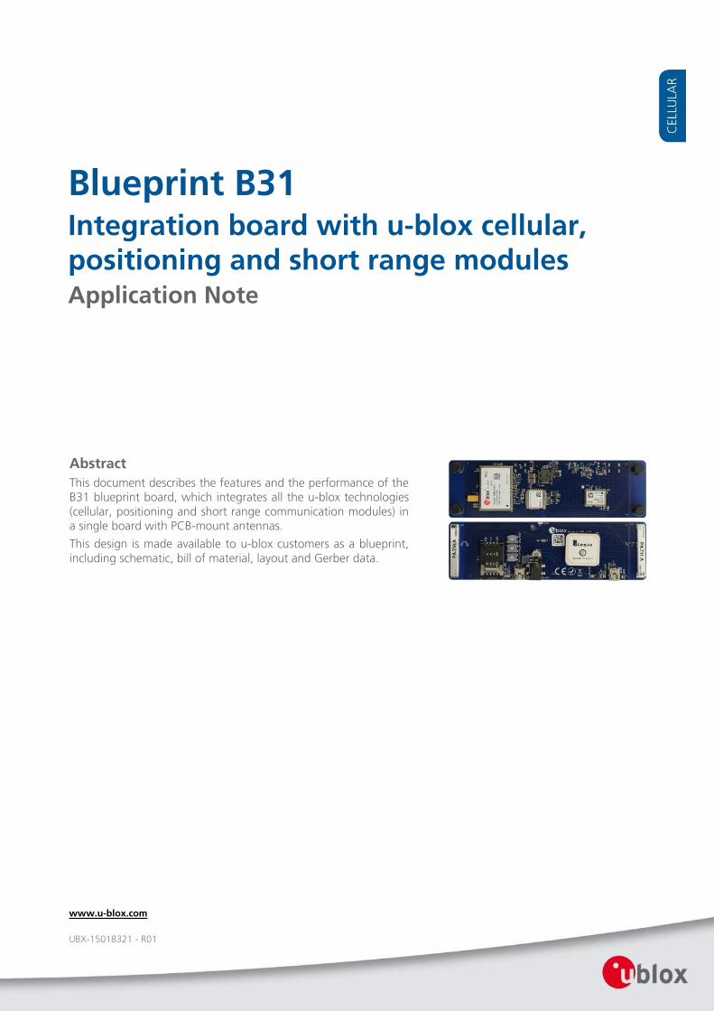
Blueprint B31 Integration board with u-blox cellular, positioning and short range modules Application Note
Abstract
This document describes the features and the performance of the B31 blueprint board, which integrates all the u-blox technologies (cellular, positioning and short range communication modules) in a single board with PCB-mount antennas.
This design is made available to u-blox customers as a blueprint, including schematic, bill of material, layout and Gerber data.
www.u-blox.com
UBX-15018321 - R01
Blueprint B31 - Application Note
UBX-15018321 - R01
Page 2 of 46
Document Information
Title Blueprint B31
Subtitle Integration board with u-blox cellular, positioning and short range modules
Document type Application Note
Document number UBX-15018321
Revision, date R01 13-Oct-2015
Document status Advance Information
Document status explanation
Objective Specification Document contains target values. Revised and supplementary data will be published later.
Advance Information Document contains data based on early testing. Revised and supplementary data will be published later.
Early Production Information Document contains data from product verification. Revised and supplementary data may be published later.
Production Information Document contains the final product specification.
This document applies to the following products:
Product Name
B31 variant L1
B31 variant L2-US
B31 variant L2-EU
u-blox reserves all rights to this document and the information contained herein. Products, names, logos and designs described herein may in whole or in part be subject to intellectual property rights. Reproduction, use, modification or disclosure to third parties of this document or
any part thereof without the express permission of u-blox is strictly prohibited.
The information contained herein is provided “as is” and u-blox assumes no liability for the use of the information. No warranty, either
express or implied, is given, including but not limited, with respect to the accuracy, correctness, reliability and fitness for a particular purpose of the information. This document may be revised by u-blox at any time. For most recent documents, please visit www.u-blox.com.
Copyright © 2015, u-blox AG
u-blox® is a registered trademark of u-blox Holding AG in the EU and other countries. All other registered trademarks or trademarks
mentioned in this document are property of their respective owners.
Blueprint B31 - Application Note
UBX-15018321 - R01 Advance Information Preface
Page 3 of 46
Preface u-blox Technical Documentation As part of our commitment to customer support, u-blox maintains an extensive volume of technical documentation for our products. In addition to our product-specific technical data sheets, the following manuals are available to assist u-blox customers in product design and development.
AT Commands Manual: This document provides the description of the AT commands supported by u-blox cellular modules.
System Integration Manual: This document describes u-blox cellular modules from the hardware and the software point of view. It provides hardware design guidelines for the optimal integration of the cellular module in the application device and it provides information on how to set up production and final product tests on application devices integrating the cellular module.
Application Notes: These documents provide guidelines and information on specific hardware and/or software topics on u-blox cellular modules. See the Related documents section for a list of documents related to your cellular module.
How to use this Application Note The Blueprint B31 Application Note provides the necessary information to successfully design in and configure the u-blox cellular, short range and positioning modules.
This Application Note has a modular structure. It is not necessary to read it from the beginning to the end.
The following symbols are used to highlight important information within the manual:
An index finger points out key information pertaining to module integration and performance.
A warning symbol indicates actions that could negatively impact or damage the module.
Questions If you have any questions about u-blox modules, please:
Read this application note and the available technical documentation carefully.
Contact our information service on the homepage http://www.u-blox.com
Technical Support
Worldwide Web
Our website (www.u-blox.com) is a rich pool of information. Product information, technical documents can be accessed 24h a day.
By E-mail
If you have technical problems or cannot find the required information in the provided documents, contact the closest Technical Support office. To ensure that we process your request as soon as possible, use our service pool email addresses rather than personal staff email addresses. Contact details are at the end of the document.
Helpful Information when Contacting Technical Support
When contacting Technical Support, have the following information ready:
Module type (e.g. TOBY-L200) and firmware version
Module configuration
Clear description of your question or the problem
A short description of the application
Your complete contact details
Blueprint B31 - Application Note
UBX-15018321 - R01 Advance Information Contents
Page 4 of 46
Contents
Preface ................................................................................................................................ 3
Contents .............................................................................................................................. 4
1 Introduction .................................................................................................................. 6
1.1 Variants ................................................................................................................................................ 6
1.2 Photo ................................................................................................................................................... 7
2 Board description ......................................................................................................... 8
2.1 Block diagram ....................................................................................................................................... 8
2.2 Environmental data .............................................................................................................................. 9
2.3 Mechanical dimensions and PCB details ................................................................................................ 9
2.4 Power supply ........................................................................................................................................ 9
2.5 Data interfaces ..................................................................................................................................... 9
2.5.1 Cellular data interfaces .................................................................................................................. 9
2.5.2 GNSS data interfaces ................................................................................................................... 10
2.5.3 Short range data interfaces ......................................................................................................... 10
2.6 Buttons, LEDs and jumpers ................................................................................................................. 10
2.7 Antenna interface ............................................................................................................................... 11
3 Board design solutions .............................................................................................. 12
3.1 Power supply design ........................................................................................................................... 12
3.1.1 Main power supply ...................................................................................................................... 12
3.1.2 Cellular module supply ................................................................................................................ 13
3.1.3 Positioning module supply ........................................................................................................... 14
3.1.4 Short range module supply .......................................................................................................... 15
3.2 Connections among subsystems ......................................................................................................... 16
3.3 Antenna design .................................................................................................................................. 17
3.3.1 Cellular antenna design ............................................................................................................... 17
3.3.2 GNSS antenna design .................................................................................................................. 19
3.3.3 Wi-Fi antenna design ................................................................................................................... 20
3.4 Layout guidelines ................................................................................................................................ 20
3.5 ESD and EMI protections .................................................................................................................... 21
4 Antenna measurements ............................................................................................. 22
4.1 Cellular antenna ................................................................................................................................. 22
4.2 GNSS antenna .................................................................................................................................... 24
4.3 Wi-Fi antenna ..................................................................................................................................... 25
5 Cellular RF performance ............................................................................................. 27
5.1 OTA testing ........................................................................................................................................ 27
5.2 RSE testing ......................................................................................................................................... 30
Blueprint B31 - Application Note
UBX-15018321 - R01 Advance Information Contents
Page 5 of 46
6 GNSS-cellular coexistence tests ................................................................................. 34
7 Delivered package ...................................................................................................... 43
Appendix .......................................................................................................................... 44
A List of acronyms ......................................................................................................... 44
Related documents .......................................................................................................... 45
Revision history ................................................................................................................ 45
Contact .............................................................................................................................. 46
Blueprint B31 - Application Note
UBX-15018321 - R01 Advance Information Introduction
Page 6 of 46
1 Introduction Blueprint B31 is a solution to integrate u-blox technologies (cellular, positioning and short range) in a single board with PCB-mount antennas. The B31 board represents a tested and optimized design, in a small form factor, which main goals are the following:
Provide a reference for combined integration of u-blox cellular, positioning, and short range modules
Give an example of components choice, placement, and layout
Address the RF and hardware challenges related to the integration of on-board antennas
The RF characteristics of the board have been carefully analyzed and optimized to:
Guarantee the best performance with all the technologies
Minimize the interference among technologies (coexistence scenarios)
Blueprint B31 is compliant with the RF requirements imposed by the main North American and European certification schemes. To verify this compliance, parameters like Total Radiated Power (TRP), Total Isotropic Sensitivity (TIS) and Radiated Spurious Emissions (RSE) have been tested in a fully anechoic chamber.
This application note provides indications about the hardware solutions implemented in the board and shows the results of the testing performed on the unit.
1.1 Variants
Table 1 reports the different variants of the blueprint B31 along with the list of integrated modules.
Variant Cellular module Short Range module Positioning module
L1 TOBY-L100-00S - NEO-M8N-0
L2-US TOBY-L200-02S ELLA-W131-00B NEO-M8N-0
L2-EU TOBY-L210-02S ELLA-W131-00B NEO-M8N-0
Table 1: Variants of the blueprint B31
Variant L1 is designed to operate in the North American market, under the Verizon cellular network, and supports only LTE and positioning functionalities.
Variants L2-US and L2-EU integrate TOBY-L2 series modules and supports cellular, positioning and Wi-Fi functionalities; the cellular functionality provides LTE, WCDMA and GSM/GPRS multi-mode technology. Variant L2-US is mainly designed for operation in America, whereas variant L2-EU is mainly designed for operation in Europe, Asia and other countries.
The positioning functionality is provided by the NEO-M8N series modules that support concurrent GPS, GLONASS, BeiDou, QZSS, SBAS and Galileo systems.
The short range module ELLA-W131 supports single band 2.4 GHz Wi-Fi functionality according to 802.11 b/g/n standards. The Bluetooth functionality of the ELLA-W131 series modules is not supported in the Blueprint B31.
For a complete description of the funcionalities supported by each module, see the TOBY-L1 / MPCI-L1 System Integration Manual [1], TOBY-L2 / MPCI-L2 System Integration Manual [2], NEO-M8 Hardware Integration Manual [3] and ELLA-W1 Data Sheet [4].

Blueprint B31 - Application Note
UBX-15018321 - R01 Advance Information Introduction
Page 7 of 46
1.2 Photo
Figure 1: Top side image of the B31 variant L2-EU
Figure 2: Bottom side image of the B31 variant L2-EU

Blueprint B31 - Application Note
UBX-15018321 - R01 Advance Information Board description
Page 8 of 46
2 Board description
2.1 Block diagram
Figure 3 and Figure 4 show the block diagram representations of the L1 and L2-EU / L2-US variants.
Switching regulator
12V
TOBY-L1
V_INTLED
SIM card
3.8V
Cellular on-board antennas
LDO3.0V
USB interface
SAW
filter
GNSS on-board
antennaSCLLED
3.3V 5V
Power supply12VDC
ON LED
PWR_ON button
RESET_Nbutton
USB interface
USB_CELLED
GNSS_SUP LED
TXD1LED
TimepulseLED
GNSS_EN jumper
LDO
NEO-M8N
USB_GNSSLED
Figure 3: Block diagram of the Blueprint B31 variant L1
Switching regulator
12V
TOBY-L2
V_INTLED
SIM card
3.8V
Cellular on-board antennas
LDO3.0V
USB interface
SAW filter
GNSS on-board antenna
V_INT
SCLLED
ELLA-W1
SDIO interface
3.3V 5V
1.8V
BTLED
WIFI ENABLE
LDO
LDO
3.3V
WiFi on-board
antenna
Power supply12VDC
ON LED
PWR_ON
button
RESET_N
button
USB interface
USB_CEL
LED
GNSS_SUP LED
TXD1LED
TimepulseLED
I2C and GPIOs
GNSS_EN jumper
WIFILED
SHO_RESETbutton
BAWFilter
Voltage
translators
LDO
NEO-M8N
USB_GNSSLED
Figure 4: Block diagram of the Blueprint B31 variants L2-EU and L2-US
Blueprint B31 - Application Note
UBX-15018321 - R01 Advance Information Board description
Page 9 of 46
2.2 Environmental data
The Blueprint board B31 is intended to operate in the temperature range –40 °C to 85 °C.
2.3 Mechanical dimensions and PCB details
The form factor used by the Blueprint B31 is 46 x 146 mm. These dimensions guarantee the optimal placement of the two cellular antennas and the best MIMO performance in case of operation in LTE mode.
The board size also allows the proper placement of the GNSS and Wi-Fi antennas, providing good levels of isolation among the radiating elements.
The PCB has a 6-layer stack-up, with most of the routing traced in the inner layers. This solution offers the best level of immunity against EMC and spurious emissions.
Components are placed on both sides of the board:
On the top layer there are the antennas, the USB interfaces, the main power supply connector, all the buttons, LEDs and jumpers.
The bottom layer accommodates the modules along with part of the supply circuitry and interfaces’ related components.
2.4 Power supply
Blueprint B31 is supplied by a typical DC voltage of 12 V and it accepts supply voltages up to 18 V. Power supply SMD connector is placed on the top layer of the board.
A main switching step-down regulator is used to provide a regulated voltage for the cellular module and for the Low Drop-Out regulators that in turn supply the short range and positioning modules. See section 2.1 and the design description in section 3.1 for more details on block diagrams.
2.5 Data interfaces
2.5.1 Cellular data interfaces
The cellular interfaces externally available for the user are:
High-speed USB 2.0 interface, with maximum 480 Mb/s data rate. This is the main interface for transferring data with a host application processor and can be used for AT commands, data communication, FW upgrade by means of the u-blox EasyFlash tool and diagnostic purposes
SIM card interface; both 1.8 V and 3 V SIM types are supported
On the L2-US and L2-EU variants, the following additional interfaces are internally used to communicate with the other subsystems of the board:
SDIO interface for communication between the cellular and the short range module
I2C interface for communication between the cellular and the positioning module.
TOBY-L2 "02" product versions do not support the communication with u-blox GNSS receivers over DDC (I
2C) interface, and therefore do not support the AssistNow aiding and the CellLocate
® features. Such
functionalities will be available with the next product versions of the TOBY-L2 series. The B31 Blueprint board already includes the necessary components and implements all the proper connections between cellular and positioning modules.

Blueprint B31 - Application Note
UBX-15018321 - R01 Advance Information Board description
Page 10 of 46
2.5.2 GNSS data interfaces
The externally available interface of the positioning module is the:
USB 2.0 full speed (12 Mb/s) compatible interface. An LDO connected to the USB interface (VBUS signal) is integrated on the board to comply with the physical characteristics of the USB 2.0 specification.
As reported in section 2.5.1, I2C interface connections for serial communication with u-blox cellular module is
present on the board variants L2-EU an L2-US, even though GNSS control feature is not supported by product version "02" of TOBY-L2 series modules.
2.5.3 Short range data interfaces
An external interface connected to the Wi-Fi module is not available. The SDIO interface is the only interface used for communication between the cellular module and the short range module. Combining a u-blox cellular module with a u-blox short range module gives the user full access to the Wi-Fi module via the cellular module USB interface.
2.6 Buttons, LEDs and jumpers
Several buttons, LEDs and jumpers are provided in the B31 blueprint board for indications or manual operations on the unit, as described in Table 2.
Name Element Description
ON LED Signals that a proper voltage level has been provided to the board
V_INT LED Turns on when the cellular module switches-on
NETWK_IND LED Cellular network status indication. According to the supported functionalities and configurations, the
cellular module may signal: no service, registered under the home network, roaming, call enabled
USB_CEL LED Indicates that a USB cable is connected to the cellular USB port
GNSS_SUP LED Turns on when the LDO that supplies the positioning module is enabled
SCL LED Shows the activity of the clock line SCL of the I2C interface, driven by the cellular module (functionality
currently not implemented)
TXD1 LED Indicates that the positioning module has data to transmit
TIMEPULSE LED Connected to the TIMEPULSE line of the positioning module, it is configured by default to one pulse
per second
USB_GNSS LED Indicates that a USB cable is connected to the positioning USB port
WIFI LED Wi-Fi status led
BT LED Bluetooth status led (functionality currently non implemented)
PWR_ON Button Allows user to force to ground the cellular PWR_ON line; the effect depends on the B31 variant (see
the section 3.1.2)
RESET_N Button Allows user to force to ground the cellular RESET_N line; the effect depends on the B31 variant (see the section 3.1.2)
SHO_RESET Button Forces the RESETn line of the short range module to ground, causing a module hardware reset
GNSS_EN Jumper Enables the LDO that supplies the positioning module, forcing the module to switch-on
Table 2: Description of the LEDs, buttons, and jumpers available on the Blueprint B31
Blueprint B31 - Application Note
UBX-15018321 - R01 Advance Information Board description
Page 11 of 46
2.7 Antenna interface
Blueprint B31 integrates four different SMD-mount antennas:
Two multiband ceramic antennas connected to the primary and secondary antenna pins of the cellular module
One patch antenna working in the frequency range of the positioning systems
One ceramic miniature antenna tuned to the Wi-Fi 2.4 GHz band

Blueprint B31 - Application Note
UBX-15018321 - R01 Advance Information Board design solutions
Page 12 of 46
3 Board design solutions
3.1 Power supply design
3.1.1 Main power supply
The main power supply of the board is a DC/DC step-down switching regulator, powered at the typical DC voltage of 12 V. The voltage level present at the output of the step-down regulator is used to directly supply the cellular module; this output voltage is set to 3.85 V typical in all the blueprint variants.
The implemented solution is the typical choice when the available primary supply source has a nominal voltage much higher than the operating voltage of intended load. In these cases a switching step-down is the best solution in terms of power efficiency and current draw.
For general design guidelines regarding the integration of a switching regulator, refer to TOBY-L1 / MPCI-L1 series System Integration Manual [1] and TOBY-L2 / MPCI-L2 series System Integration Manual [2].
The selected step-down switching regulator is the Linear Technology LT3972 that guarantees high efficiency and low ripple of the output voltage. Figure 5 shows the schematic of the main power supply implemented in the Blueprint B31.
Figure 5: Main power supply schematic
The LT3972 works in PWM mode and the value of the switching frequency is regulated by means of the resistor connected to the RT pin (R26); two different solutions are implemented:
Variant L1: the switching frequency is set to 290 kHz. The low value of the switching frequency has been selected to maximize cellular over the air performance, specifically the TIS parameter in the LTE band 13. When integrating TOBY-L100 and a step-down regulator, set the switching frequency of the regulator below 500 kHz to maximize the sensitivity of the cellular module.
Variants L2-US and L2-EU: the switching frequency is set to 1.4 MHz to guarantee good modulation spectrum performance when the cellular module operates in the 2G mode.
Additional precautions are implemented in the main power supply circuitry:
Diode D3 is a protection against over-voltages and reverse voltages
C16, C17, L1, C19, C100, L2 network is a 2-stage low-pass filter implemented to minimize conducted emissions on the input power source line
The voltage rating of the components are selected to withstand voltage spikes in the input power supply

Blueprint B31 - Application Note
UBX-15018321 - R01 Advance Information Board design solutions
Page 13 of 46
3.1.2 Cellular module supply
The cellular module is directly supplied by the step-down regulator IC6. On the VCC supply pins of the cellular module the following components are placed as described in Figure 6:
Tantalum capacitor C54, mounted on the variants L2-EU and L2-US only, is used to avoid voltage drop undershoot and overshoot at the start and end of a transmit burst during a GSM call
Ceramic capacitors C30-C34 provide filtering against EMI in the frequency bands of operation of the cellular module
Ferrite bead L80 (BLM18EG221SN1) is integrated in all the blueprint variants to “clean” the voltage line and suppress noise
Figure 6: Cellular module power supply input schematic detail
3.1.2.1 Switch-on and switch-off of the cellular module
Depending on the variant, the cellular module can be switched-on as follows:
Variant L1: apply a valid power supply at the blueprint power connector, then press the PWR_ON button
Variants L2-US and L2-EU: cellular module automatically switches-on once a valid voltage is applied to the board power connector
To switch-off the cellular module perform the following actions with all the variants:
Send the AT+CPWROFF command then remove the main power supply from the board
For a complete description of all the operating modes of the cellular modules and the transitions from a state to another, see the TOBY-L1 / MPCI-L1 series System Integration Manual [1] and TOBY-L2 / MPCI-L2 series System Integration Manual [2].
3.1.2.2 RESET_N and PWR_ON buttons
RESET_N and PWR_ON buttons operates according to the specific variant of the Blueprint B31, as reported in Table 3.
Button Variant L1 Variants L2-US and L2-EU
RESET_N Causes an abrupt hardware shutdown of the cellular module.
To switch-on the module again, press the PWR_ON button.
Causes an abrupt hardware reset of the cellular module.
PWR_ON Used to switch-on the cellular module when a proper voltage
is present at the board power connector.
Can be used to switch-on the cellular module again after
RESET_N button has been pressed.
Used to switch-on the cellular module once AT+CPWROFF
command is sent and the board main power supply is still
present.
Table 3: Effects of the PWR_ON and RESET_N buttons on the blueprint variants
Blueprint B31 - Application Note
UBX-15018321 - R01 Advance Information Board design solutions
Page 14 of 46
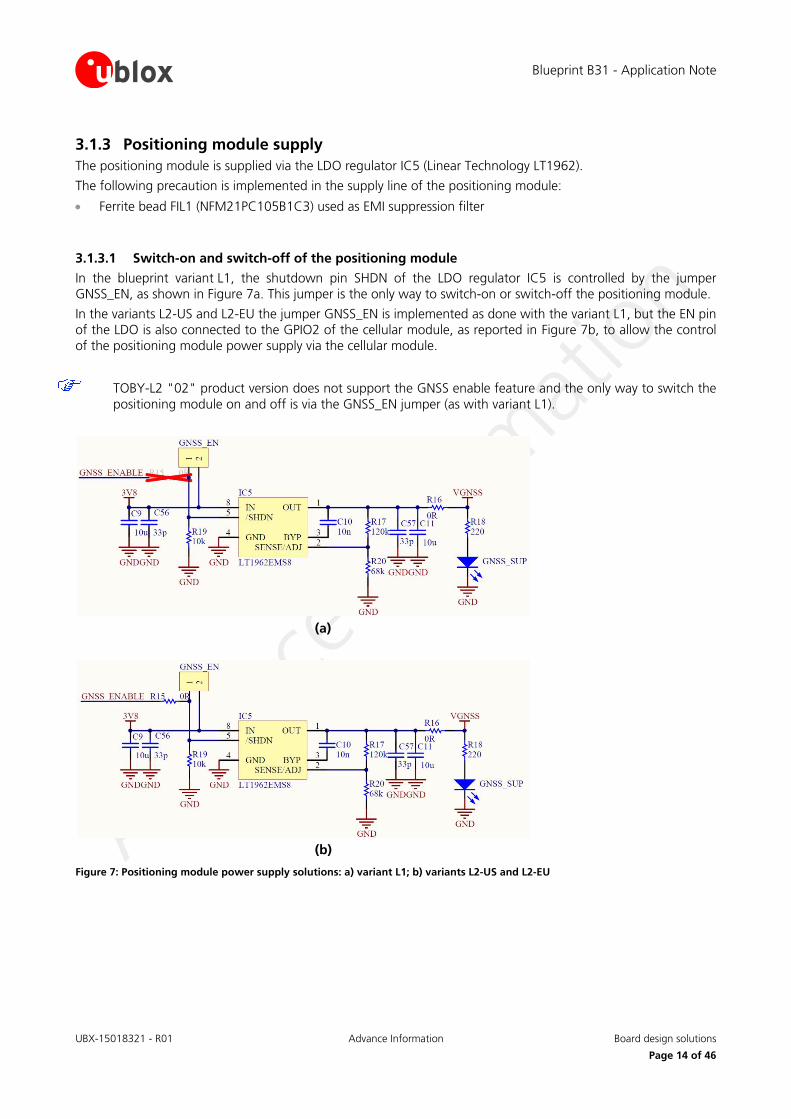
3.1.3 Positioning module supply
The positioning module is supplied via the LDO regulator IC5 (Linear Technology LT1962).
The following precaution is implemented in the supply line of the positioning module:
Ferrite bead FIL1 (NFM21PC105B1C3) used as EMI suppression filter
3.1.3.1 Switch-on and switch-off of the positioning module
In the blueprint variant L1, the shutdown pin SHDN of the LDO regulator IC5 is controlled by the jumper GNSS_EN, as shown in Figure 7a. This jumper is the only way to switch-on or switch-off the positioning module.
In the variants L2-US and L2-EU the jumper GNSS_EN is implemented as done with the variant L1, but the EN pin of the LDO is also connected to the GPIO2 of the cellular module, as reported in Figure 7b, to allow the control of the positioning module power supply via the cellular module.
TOBY-L2 "02" product version does not support the GNSS enable feature and the only way to switch the positioning module on and off is via the GNSS_EN jumper (as with variant L1).
(a)
(b)
Figure 7: Positioning module power supply solutions: a) variant L1; b) variants L2-US and L2-EU

Blueprint B31 - Application Note
UBX-15018321 - R01 Advance Information Board design solutions
Page 15 of 46
3.1.4 Short range module supply
The short range module is integrated in the variants L2-US and L2-EU; its power supply is controlled by two LDO regulators (Microchip MCP1824, IC7 and IC8) that provide two regulated voltage domains at 3.3 V and 1.8 V.
The reference voltage level of the module digital pins is set to 1.8 V (see Figure 8).
3.1.4.1 Switch-on and switch-off of the short range module
The short range module can be switched-on or switched-off exclusively by the cellular module that controls:
The enable EN pin of the LDO regulators IC7 and IC8. The supply output pin V_INT of the cellular module is connected to the enable pin of the two LDO regulators with appropriate pull-down resistors to avoid an improper switch-on of the short range module before the switch-on of V_INT
The power-down input pin PDn of the short range module. The GPIO1 pin of the cellular module is connected to the active low power-down input pin (PDn) of the short range module.
The Wi-Fi enable functionality implemented through the GPIO1 pin is available on Blueprint B31 variants L2-US and L2-UE.
Figure 8 shows the schematic portion related to the short range power supply design.
Figure 8: Short range module power supply solution
The sleep clock SLEEP_CLK input pin of the short range module is left not connected, since the sleep-mode functionality is not supported by current FW version. The external oscillator, required to operate in low-power mode, is currently not mounted in all the blueprint variants.
The configuration CFG pin of the short range module is connected to ground by means of a proper pull-down resistor since the module operates without sleep clock.
3.1.4.2 SHO_RESET button
SHO_RESET button can be used to trigger an abrupt hardware shutdown of the short range module. Since the RESET pin of the short range module has a weak internal pull-up to VIO pin, an external pull-up to the 1.8 V supply rail has been provided.

Blueprint B31 - Application Note
UBX-15018321 - R01 Advance Information Board design solutions
Page 16 of 46
3.2 Connections among subsystems Blueprint variants L2-US and L2-EU implement connections between the cellular module and the short range module and between cellular and positioning modules.
In the blueprint design, the short range module is fully controlled via the cellular module; with this solution designers have full access to the short range module via dedicated AT commands sent to the cellular USB interface; there is no need for a second interface connected to the short range module.
Short range-related messages are sent from the cellular module to the short range module via a dedicated SDIO interface, as illustrated in Figure 8. On the SDIO lines, appropriate low value series damping resistors are integrated to avoid reflections or other losses in signal integrity, which may create ringing and loss of a square wave shape.
The most appropriate value of the series damping resistors depends on the specific lines length and layout implemented. In general, the SDIO series resistors are not strictly required, but it is recommended to slow the SDIO signal, for example with 22 Ω or 33 Ω resistors; these avoid any possible ringing problem without violating the rise / fall time requirements.
Figure 9: Elements involved in the communication between cellular and positioning modules
GNSS control via cellular module is not supported by "02" product version of TOBY modules, yet the variants L2-US and L2-EU implement all the required components to allow this control. This functionality will be integrated in next product versions of the cellular module.
Figure 9 shows the elements used to connect the cellular module with the positioning module:
I2C pins of the cellular module are connected to the related pins of the positioning module. Since cellular I
2C
interface is not tolerant up to 3.0 V, the connection between modules must pass through an I2C-bus
bidirectional voltage translator with proper pull-up resistors, like the Texas Instruments TCA9406 (IC1)
GPIO2 pin of the cellular module is connected to the shutdown SHDN input pin of the LDO regulator IC5, switching on / off the power supply of the positioning module, implementing the "GNSS enable" function
The V_BCKP supply output pin of the cellular module is directly connected to the V_BCKP backup supply input pin of the GNSS receiver, in order to enable warm and hot start features on the positioning module
The GPIO3 and GPIO4 pins of the cellular module are connected to the TxD and EXTINT pins of the positioning module via a proper unidirectional general purpose voltage translator, the Texas Instruments SN74AVC2T245 (IC2), and these lines provide the GNSS data ready and GNSS RTC sharing functionalities.

Blueprint B31 - Application Note
UBX-15018321 - R01 Advance Information Board design solutions
Page 17 of 46
3.3 Antenna design
The most important topic in the design of the Blueprint B31 is the optimization of the RF performance; specifically the challenge is how to integrate four different antennas in a small PCB, maintaining good radiation properties with all the technologies. Sections below discuss the main design choices implemented.
3.3.1 Cellular antenna design
Two radiating elements are required to comply with the MIMO requirements of TOBY-L series modules. Board dimensions have been defined to minimize the PCB size and guarantee RF performance of two cellular antennas.
As general guidelines, the antenna selection process must take into account the following parameters:
Operating band: it is usually expressed as the frequency span where the VSWR (or S11), at the antenna port, is lower than a certain level. The recommended value is VSWR < 2, acceptable is VSWR < 3
Efficiency: is the ratio of the radiated power to the power delivered to the antenna input; it is an average measure of how well an antenna receives or transmits. Efficiencies greater than 50% are acceptable, greater than 70% are recommended
Gain: is the efficiency multiplied by the directivity; it is a measure of how the antenna is able to direct radiation towards a certain direction (usually the direction of maximum transmission / reception). Antenna maximum gain must not exceed the limiting values reported in the system integration manual of the cellular module [1], [2] and imposed by the regulatory certification schemes
Antenna pattern: is the variation of the power radiated by the antenna as a function of the direction. For cellular applications it is convenient to select antennas with a "donut shaped" or toroidal radiation pattern; this guarantees a good reception in almost all the directions
In case of MIMO applications, where two cellular antennas are integrated on the same board, additional elements must be considered:
Isolation between antennas; 15 dB isolations measured between antennas ports is recommended, 10 dB of isolation is acceptable.
Un-correlation, i.e. difference in the antennas radiation patters and / or polarizations
To maximize the parameters above, antennas position on the board must be accurately defined. As a general guideline, separation distance of at least 1/4 of the wavelength of the minimum operating frequency should be provided, but this is not the only factor and in most of the cases simulations and measurements are necessary to define the best antenna location on the PCB.
When integrating PCB-mount antennas or internal antennas with small RF coaxial cables, the effect of the board ground plane must be considered, since antenna parameters are affected by the ground plane size. Typically, the antenna gain and the antenna efficiency values drop when the PCB dimensions are reduced.
Finally, antennas characteristic impedance must be matched with matching network components that tweak the VSWR and avoid additional losses.
The integration of two cellular antennas must be carefully evaluated since it imposes additional requirements and design challenges; in this case it is highly recommended to work with the antenna manufacturer and to take care of the radiating aspects at the very beginning of the product definition.
Radiation performance is subject to measurements according to approval requirements of specific network operators (mainly in the North American market) or regulatory authorities. In these cases additional certification requirements apply and customers are typically asked to evaluate their device in terms of:
TRP: Total Radiated Power; is a measure of how much power is radiated by the device (transmitter test)
TIS: Total Isotropic Sensitivity; is a measure of the minimum received power required to maintain a specific error rate (receiver test)

Blueprint B31 - Application Note
UBX-15018321 - R01 Advance Information Board design solutions
Page 18 of 46
RSE: Radiated Spurious Emissions; takes into account the power emitted outside the RF operating band. Power limits are imposed by the regulatory authorities to avoid harmful interferences
Blueprint B31 has been specifically designed to get good RF performance and the TRP, TIS and RSE values have been measured to verify compliance to the main certification schemes, as reported in section 4.1.
All the variants of the Blueprint B31 integrate the following cellular antennas:
Taoglas PA.710.A, used and the cellular primary Tx / Rx antenna
Taoglas PA.711.A, used as the cellular secondary / MIMO antenna (Rx only)
Each radiating element is a PCB-mount ceramic antenna working in the GSM / WCDMA / LTE frequency bands from 698 MHz to 960 MHz and from 1710 MHz to 2690 MHz. The PA.710.A and PA.711.A antennas are designed to operate together in LTE / MIMO applications and to maximize the parameters described above.
Based on the indications provided by the antenna manufacturer, the PCB dimensions chosen for the Blueprint B31 are: 46 x 146 mm. The placement of the antennas on the board is shown in Figure 10. The radiating elements are placed on the opposite small edges of the board, at a distance of around 132 mm.
Primary antenna Secondary antennaPrimary RF path Secondary RF path
Cellular module (bottom side)
132 mm
146 mm
46
mm
Figure 10: Cellular antennas and RF paths placement on top side, and cellular module placement on bottom side
As shown in Figure 10, the cellular antennas are placed on the top layer of the board, whereas the cellular module is located on the bottom side. The RF paths of the primary and secondary antennas are routed on the top layer of the board, using a grounded coplanar waveguide with the following parameters:
waveguide width: 0.38 mm
gap width: 0.40 mm
dielectric thickness: 0.27 mm
The electric permittivity of the dielectric material is 4.2; the reference ground plane of the waveguide is the first inner layer. These design parameters guarantee a characteristic impedance of 50 Ω for the RF path.
The RF path of the primary antenna is much shorter than the secondary RF path and is routed close to the primary antenna.
When designing the antenna layout and placement, attention must be paid on the clearance area requirements and on the placement of the matching components, as reported in the antenna datasheet.

Blueprint B31 - Application Note
UBX-15018321 - R01 Advance Information Board design solutions
Page 19 of 46
3.3.2 GNSS antenna design
The positioning module NEO-M8N, integrated in all the blueprint variants, is a concurrent GNSS receiver, able to receive and track multiple GNSS systems: GPS, GLONASS, BeiDou, QZSS, SBAS and Galileo. Because of the dual-frequency RF front-end architecture of the module, two of the three signals (GPS L1C/A, GLONASS L1OF and BeiDou B1) can be received and processed concurrently. By default, the positioning module is configured for concurrent GPS (including SBAS and QZSS) and GLONASS reception.
For these reasons the antenna integrated in the board is a ceramic patch antenna working in the GSP / GLONASS / BEIDOU frequency bands but tuned to better operate in the GPS – GLONASS frequency range: 1570 – 1610 MHz. The selected part number is:
Taoglas CGGBP.25.4.A.02, 25 x 25 x 4 mm
The placement of the patch antenna on the board affects the RF performance. The GNSS antenna, as reported in Figure 11, is placed on the top layer, in an area free from components or noisy lines. The positioning module is placed on the opposite side, directly beneath the patch antenna, in order to minimize the length of the antenna RF path and the associated losses.
A GNSS passive antenna requires a careful evaluation of the layout of the RF section. Typically, a passive antenna may be located near electronic components; therefore, care should be taken to reduce electrical noise that may interfere with the antenna performance. The GNSS antenna is located far away from the cellular primary Tx/Rx antenna, in order to minimize the inference / blocking effect of the cellular signals.
Since the GNSS sensitivity of the board is related to the ground plane size, the ground size on the top layer has been maximized; moreover, the area underneath the ceramic patch is fully covered by stitching GND vias.
GNSS antenna
SAW filter (bottom side)
Positioning module (bottom side)
Figure 11: GNSS antenna placement on top side, and positioning module and SAW filter placement on bottom side
As described in the NEO-M8 Hardware Integration Manual [3], the positioning module NEO-M8N is equipped with an internal SAW filter and an internal LNA. Due to the small dimensions of the blueprint board and due to the coexistence of cellular and Wi-Fi technologies that may concurrently transmit and receive, an additional countermeasure has been adopted:
SAW filter Tai-Saw TA1343A, operating in the GSP / GLONASS / BEIDOU frequency bands
The SAW filter is placed between the patch antenna and the antenna pin of the positioning module.

Blueprint B31 - Application Note
UBX-15018321 - R01 Advance Information Board design solutions
Page 20 of 46
3.3.3 Wi-Fi antenna design
The short range module ELLA-W131, integrated in the blueprint variants L2-US and L2-EU, supports Wi-Fi and Bluetooth functionalities in the 2.4 GHz radio band (2.402 – 2.492 GHz).
The antenna connected at the ANT pin of the short range module is:
Taoglas WLA.01 2.4GHz loop SMD antenna, 3.2 x 1.6 x 0.5 mm
Antenna matching components and proper placement on the board are essential to get good efficiency in the operating band. The location of the short range antenna on the blueprint board is illustrated in Figure 12. The antenna is designed to be mounted at the center of the long edge of the board; the distance from the other co-located antennas guarantee good concurrent performance.
Wi-Fi antennaBAW filter
Short range module (bottom side)
Figure 12: Wi-Fi antenna and BAW filter placement on top side, and short range module placement on bottom side
An additional element to be considered is the possible scenario in which the cellular module operates in the LTE band 7 (2500 - 2690 MHz): the frequency range of this band is very close to the Wi-Fi 2.4GHz band. To guarantee good Wi-Fi operation with the Cellular module transmitting in the LTE band 7, it is highly recommended to integrate a Wi-Fi / LTE band-pass coexistence filter on the short range antenna path.
In the Blueprint B31, the following component is integrated between the short range module and its antenna:
TDK EPCOS B9604 BAW filter. This Bulk Acoustic Wave filter is specifically designed to get an extremely sharp transition response and guarantees LTE-band7 / Wi-Fi 2.4 GHz coexistence.
3.4 Layout guidelines
The layout of the board directly affects antenna performance. The Blueprint B31 is design with a 6-layer stack-up; the following design choices have been implemented:
Components are mounted on both, top and bottom layers; all the antennas are placed on the top layer
The 1st internal layer is used as a ground plane layer, with minimal tracing of signal lines
The 2nd inner layer is mainly used for the tracing of the power supply lines
The 3rd inner layer is used to route the high frequency digital lines like SDIO and USB lines
The 4th inner layer is another reference ground plane
All the RF paths are grounded coplanar waveguide, with proper GND stitching vias placed along the paths
The transmission lines width and GND spacing are uniform and routed as smoothly as possible; i.e. avoiding abrupt changes of width and GND spacing
RF transmission lines are clearly separated from any possible source of radiated energy, like switching power supplies and digital lines
Blueprint B31 - Application Note
UBX-15018321 - R01 Advance Information Board design solutions
Page 21 of 46
There is no signal routing in parallel to the transmission lines or crossing the transmission lines on buried metal layers
Power supply lines are wide and as short as possible
Power supply lines are routed on a dedicated layer, separated from RF lines, RF-related components and high frequency digital lines
The length of the lines on both top and bottom layers has been minimized in order to eliminate possible sources of noise
Each GND pad surrounding the modules’ power supply pins has one or more dedicated via down to the application board solid ground layer
There are two layers of the board used as ground plane. Ground plane layers should be free from digital return currents
For improved shielding, lots of GND vias are placed around the micro strip lines, around the serial communication lines and high-frequency signal lines
All the unused PCB portions of the board layers are filled with ground pours
A fence of stitching via holes is implemented around the whole board perimeter
3.5 ESD and EMI protections
To guarantee protection against ESD, the following component is integrated on USB lines, button lines and on the mechanical switch pins of the SIM card holder:
PESD0402-140: ESD suppressor with very low shunt capacitance
EMI protections are placed on the two USB interfaces, specifically on the high frequency lines USB_D+ and USB_D-:
DLP11SA900HL2L: common mode choke coil chip
Additionally, on the SIM card lines, 47 pF bypass capacitors C35, C37, C38, C39 are mounted to avoid RF coupling.

Blueprint B31 - Application Note
UBX-15018321 - R01 Advance Information Antenna measurements
Page 22 of 46
4 Antenna measurements
4.1 Cellular antenna
The cellular antennas PA.710.A and PA.711.A require a matching network to optimize the VSWR over the whole operating frequency band. Figure 13 shows the matching components and their values.
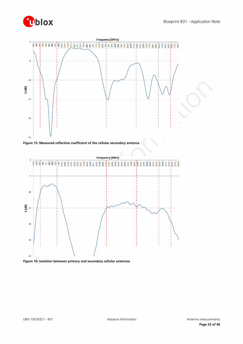
The same components are used on all the variants of the blueprint, even though further optimizations could be done in each variant in order to improve the matching on the bands of interest, reducing the performance on the not used bands. The matching circuitry proposed in Figure 13 returns a good overall matching over all the possible operating bands, as illustrated in Figure 14 and Figure 15 for the primary and secondary antenna respectively. The graphs of Figure 14 and Figure 15 represent the antenna matching in terms of the port scattering parameter S, i.e. the voltage reflection coefficient measured on the antenna RF line between the module ANT pin and the matching network.
Figure 16 shows the isolation between the two cellular antennas measured in terms of scattering parameter S. The isolation is optimal in the higher frequency bands (1710-2170 MHz and 2500-2690 MHz) whereas is below 10 dB in the lower band (704-960 MHz); the latter is due to the limited distance between antennas and cannot be further improved. In any case, the not optimal isolation in the lower band does not prevent the Blueprint B31 to comply with the typical North American operators requirements on TIS (see section 5).
Figure 13: Cellular antennas matching circuitry
Figure 14: Measured reflection coefficient of the cellular primary antenna
Blueprint B31 - Application Note
UBX-15018321 - R01 Advance Information Antenna measurements
Page 23 of 46
Figure 15: Measured reflection coefficient of the cellular secondary antenna
Figure 16: Isolation between primary and secondary cellular antennas

Blueprint B31 - Application Note
UBX-15018321 - R01 Advance Information Antenna measurements
Page 24 of 46
4.2 GNSS antenna
As described in section 3.3.2, the GNSS antenna matching is optimized for operations on the GPS – GLONASS frequency range (1570 – 1610 MHz). As reported in Figure 17, the antenna reflection coefficient is good in the frequency bands of interest. The values measured in Figure 17 are obtained without a dedicated matching network; in this case a fine tuning of the radiating element has been performed directly on the patch antenna CGGBP.25.4.A.02.
The graph in Figure 18 shows the frequency behavior of the antenna efficiency and reveals an overall good efficiency always greater than 70% in the intended bands.
A graphical 3D representation of the antenna radiation pattern is given in Figure 19 for the GPS and GLONASS center frequencies, along with the indications of the maximum antenna gains.
Figure 17: Measured reflection coefficient of the GNSS antenna
Figure 18: Measured efficiency of the GNSS antenna
Blueprint B31 - Application Note
UBX-15018321 - R01 Advance Information Antenna measurements
Page 25 of 46
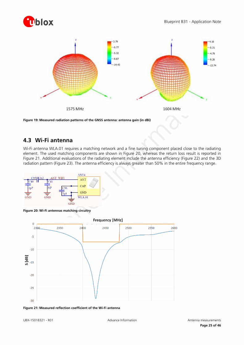
Figure 19: Measured radiation patterns of the GNSS antenna: antenna gain (in dBi)
4.3 Wi-Fi antenna
Wi-Fi antenna WLA.01 requires a matching network and a fine tuning component placed close to the radiating element. The used matching components are shown in Figure 20, whereas the return loss result is reported in Figure 21. Additional evaluations of the radiating element include the antenna efficiency (Figure 22) and the 3D radiation pattern (Figure 23). The antenna efficiency is always greater than 50% in the entire frequency range.
Figure 20: Wi-Fi antennas matching circuitry
Figure 21: Measured reflection coefficient of the Wi-Fi antenna

Blueprint B31 - Application Note
UBX-15018321 - R01 Advance Information Antenna measurements
Page 26 of 46
Figure 22: Measured efficiency of the Wi-Fi antenna
Figure 23: Measured radiation patterns of the Wi-Fi antenna: antenna gain (in dBi)

Blueprint B31 - Application Note
UBX-15018321 - R01 Advance Information Cellular RF performance
Page 27 of 46
5 Cellular RF performance The cellular RF part OF the Blueprint B31 is characterized BY MEANS of the following parameters:
Total Radiated Power (TRP)
Total Isotropic Sensitivity (TIS)
Radiated Spurious Emissions (RSE)
The first two parameters, normally referred as Over The Air (OTA) tests, are compared with North American mobile operators’ requirements; AT&T and Verizon requirements are used as a reference. A generic product integrating TOBY-L modules and operating under AT&T or Verizon networks has to execute OTA testing and specifically guarantee that both TRP and TIS are within operators’ target values. OTA testing may be challenging in case of very small devices since the reduced board size limits the antenna gain and efficiency and this in turn leads to poor TRP and TIS values. Blueprint B31 OTA values are evaluated only for the LTE technology since requirements in these bands and in this technology are, by far, the most challenging ones.
The RSE testing, on a device integrating TOBY-L modules, is always required to operate in North America, Europe and other countries. RSE is not an operator-related test, but is instead a mandatory requirement. Depending on the "country zone", different standards list RSE as a mandatory test, but almost all of these refer to the 3GPP technical specifications. Blueprint B31 has been tested according to these 3GPP rules (see section 5.2).
By comparing the Blueprint B31 OTA and RSE results against operators’ and 3GPP requirements, u-blox shows an example of integration board that fulfills the typical certification requirements for an end device; Blueprint B31 can be used as a reference for antenna integration, components selection and layout design.
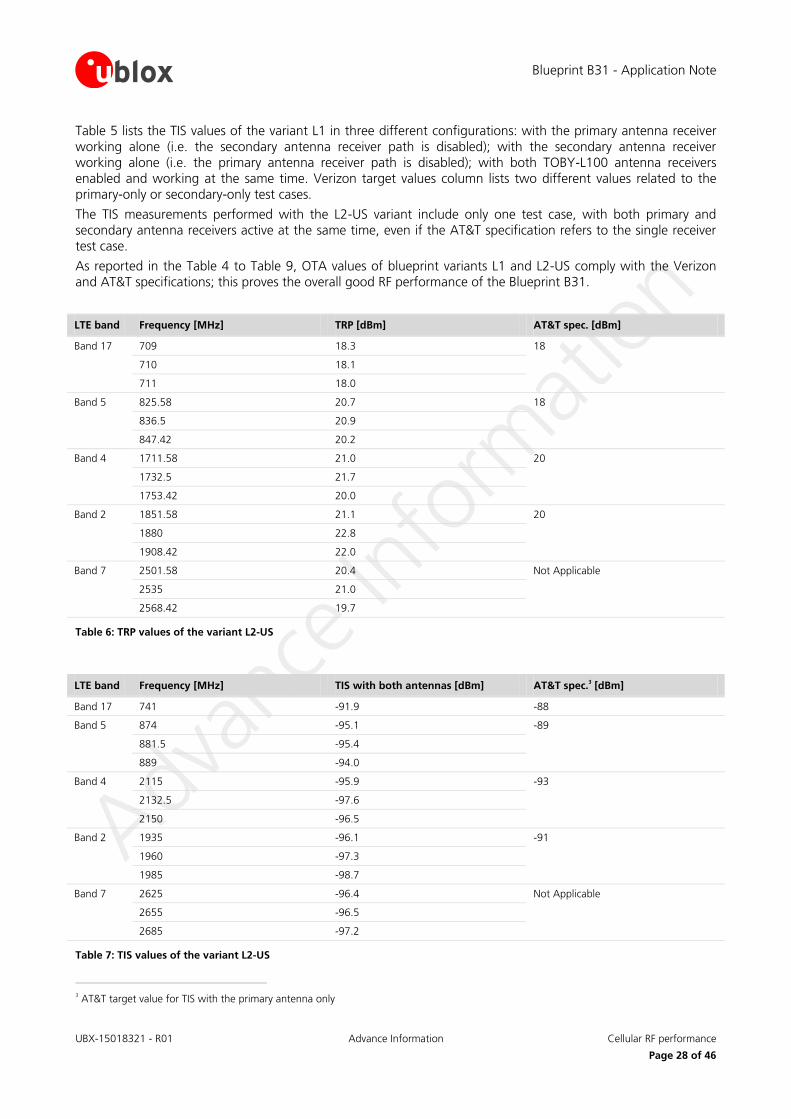
5.1 OTA testing
Blueprint B31 TRP and TIS values in the different LTE bands are reported in Table 4 and in Table 5 for variant L1, in Table 6 and Table 7 for variant L2-US. Both variants target the North American market and for this reason the required TRP/TIS values imposed by AT&T and Verizon are used to estimate the RF performance of the board. Unit has been tested according to the CTIA Test Plan for Wireless Device Over-the-Air Performance [5].
LTE band Frequency [MHz] TRP [dBm] Verizon spec. [dBm]
Band 13 778.58 20.6 18
782 20.4
785.42 20.1
Band 4 1711.58 22.1 20
1732.5 21.8
1753.42 21.8
Table 4: TRP values of the variant L1
LTE band Frequency [MHz] TIS with primary antenna only [dBm]
TIS with secondary antenna only [dBm]
TIS with both antennas [dBm]
Verizon spec. [dBm]
Band 13 751 -92.1 -91.9 -93.1 -911, -88
2
Band 4 2115 -96.7 -97.1 -97.7 -881, -85
2
2132.5 -97.9 -94.5 -99.3
2150 -98.4 -97.6 -98.9
Table 5: TIS values of the variant L1
1 Verizon target value for TIS with the primary antenna only
2 Verizon target value for TIS with the secondary antenna only
Blueprint B31 - Application Note
UBX-15018321 - R01 Advance Information Cellular RF performance
Page 28 of 46
Table 5 lists the TIS values of the variant L1 in three different configurations: with the primary antenna receiver working alone (i.e. the secondary antenna receiver path is disabled); with the secondary antenna receiver working alone (i.e. the primary antenna receiver path is disabled); with both TOBY-L100 antenna receivers enabled and working at the same time. Verizon target values column lists two different values related to the primary-only or secondary-only test cases.
The TIS measurements performed with the L2-US variant include only one test case, with both primary and secondary antenna receivers active at the same time, even if the AT&T specification refers to the single receiver test case.
As reported in the Table 4 to Table 9, OTA values of blueprint variants L1 and L2-US comply with the Verizon and AT&T specifications; this proves the overall good RF performance of the Blueprint B31.
LTE band Frequency [MHz] TRP [dBm] AT&T spec. [dBm]
Band 17 709 18.3 18
710 18.1
711 18.0
Band 5 825.58 20.7 18
836.5 20.9
847.42 20.2
Band 4 1711.58 21.0 20
1732.5 21.7
1753.42 20.0
Band 2 1851.58 21.1 20
1880 22.8
1908.42 22.0
Band 7 2501.58 20.4 Not Applicable
2535 21.0
2568.42 19.7
Table 6: TRP values of the variant L2-US
LTE band Frequency [MHz] TIS with both antennas [dBm] AT&T spec.3 [dBm]
Band 17 741 -91.9 -88
Band 5 874 -95.1 -89
881.5 -95.4
889 -94.0
Band 4 2115 -95.9 -93
2132.5 -97.6
2150 -96.5
Band 2 1935 -96.1 -91
1960 -97.3
1985 -98.7
Band 7 2625 -96.4 Not Applicable
2655 -96.5
2685 -97.2
Table 7: TIS values of the variant L2-US
3 AT&T target value for TIS with the primary antenna only
Blueprint B31 - Application Note
UBX-15018321 - R01 Advance Information Cellular RF performance
Page 29 of 46
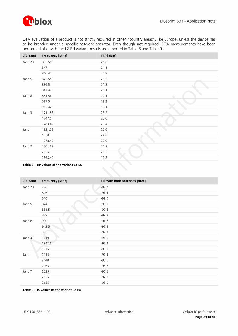
OTA evaluation of a product is not strictly required in other "country areas", like Europe, unless the device has to be branded under a specific network operator. Even though not required, OTA measurements have been performed also with the L2-EU variant; results are reported in Table 8 and Table 9.
LTE band Frequency [MHz] TRP [dBm]
Band 20 833.58 21.6
847 21.1
860.42 20.8
Band 5 825.58 21.5
836.5 21.8
847.42 21.1
Band 8 881.58 20.1
897.5 19.2
913.42 18.1
Band 3 1711.58 23.2
1747.5 23.0
1783.42 21.4
Band 1 1921.58 20.6
1950 24.0
1978.42 23.0
Band 7 2501.58 20.3
2535 21.2
2568.42 19.2
Table 8: TRP values of the variant L2-EU
LTE band Frequency [MHz] TIS with both antennas [dBm]
Band 20 796 -89.2
806 -91.4
816 -92.6
Band 5 874 -93.0
881.5 -92.6
889 -92.3
Band 8 930 -91.7
942.5 -92.4
955 -92.3
Band 3 1810 -96.1
1842.5 -95.2
1875 -95.1
Band 1 2115 -97.3
2140 -96.6
2165 -95.7
Band 7 2625 -96.2
2655 -97.0
2685 -95.9
Table 9: TIS values of the variant L2-EU
Blueprint B31 - Application Note
UBX-15018321 - R01 Advance Information Cellular RF performance
Page 30 of 46
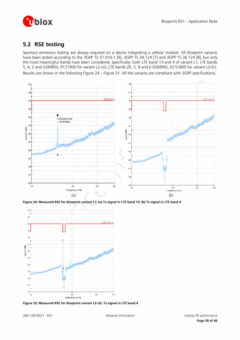
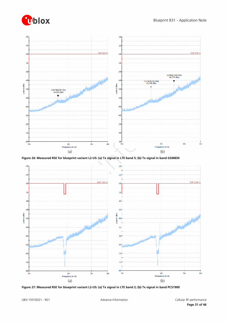
5.2 RSE testing
Spurious emissions testing are always required on a device integrating a cellular module. All blueprint variants have been tested according to the 3GPP TS 51.010-1 [6], 3GPP TS 34.124 [7] and 3GPP TS 36.124 [8], but only the most meaningful bands have been considered, specifically: both LTE band 13 and 4 of variant L1; LTE bands 5, 4, 2 and GSM850, PCS1900 for variant L2-US; LTE bands 20, 5, 8 and E-GSM900, DCS1800 for variant L2-EU.
Results are shown in the following Figure 24 – Figure 31. All the variants are compliant with 3GPP specifications.
(a) (b)
Figure 24: Measured RSE for blueprint variant L1: (a) Tx signal in LTE band 13; (b) Tx signal in LTE band 4
Figure 25: Measured RSE for blueprint variant L2-US: Tx signal in LTE band 4
Blueprint B31 - Application Note
UBX-15018321 - R01 Advance Information Cellular RF performance
Page 31 of 46
(a) (b)
Figure 26: Measured RSE for blueprint variant L2-US: (a) Tx signal in LTE band 5; (b) Tx signal in band GSM850
(a) (b)
Figure 27: Measured RSE for blueprint variant L2-US: (a) Tx signal in LTE band 2; (b) Tx signal in band PCS1900

Blueprint B31 - Application Note
UBX-15018321 - R01 Advance Information Cellular RF performance
Page 32 of 46
(a) (b)
Figure 28: Measured RSE for blueprint variant L2-EU: (a) Tx signal in LTE band 5; (b) Tx signal in LTE band 20
(a) (b)
Figure 29: Measured RSE for blueprint variant L2-EU: (a) Tx signal in LTE band 8; (b) Tx signal in band E-GSM900

Blueprint B31 - Application Note
UBX-15018321 - R01 Advance Information
Page 33 of 46
(b) (b)
Figure 30: Measured RSE for blueprint variant L2-EU: (a) Tx signal in LTE band 3; (b) Tx signal in band DCS1800
Figure 31: Measured RSE for blueprint variant L2-EU: Tx signal in LTE band 1

Blueprint B31 - Application Note
UBX-15018321 - R01 Advance Information GNSS-cellular coexistence tests
Page 34 of 46
6 GNSS-cellular coexistence tests The main goal of the Blueprint B31 is to show the possible integration of all u-blox technology in a single small board. This integration must guarantee that each module’s performance is maintained and not degraded due to the presence of the other transmitters.
In this section, the GNSS-cellular coexistence case is considered. The measurements performed aim to estimate the GNSS reception degradation when the co-located cellular module is switched-on and transmitting at a specific power level.
All tests are performed with a stationary setup, i.e. the blueprint board is placed in a fixed position and in a clear sky view condition. In order to detect the quality of the satellite reception, the blueprint board is connected to a PC and the u-blox u-center GNSS evaluation software [10] is used to record the level of the carrier-to-noise power density ratio (C/N
0) of the satellites. The positioning module returns, via u-center, the values of the
received C/N0 for the GPS, GLONASS and SBAS systems. Each test is performed using the following approach:
Blueprint board is powered and both cellular and short range modules are turned off. With this setup there are no active transmitters on the board and the positioning module can record the C/N
0 levels, used as a
reference (or optimal) condition. In the following graphs, this measurement condition is labelled "GNSS Alone".
After the first reference measurement, the cellular module is switched-on and set to transmit at a fixed power level. This can be done using the +UTEST AT commands; for more details see the End User Test Application Note [9]. To stress the GNSS signal reception, the cellular module is set to transmit at the maximum available power, according to the used technology (GSM, WCDMA or LTE).
For each cellular band available, the TOBY-L module is forced to transmit in the low, mid and high channels.
If a sensible degradation in the C/N0 reception occurs, the cellular output power is lowered and tests
repeated again.
A new "Stand Alone" measurement is collected before proceeding with a new cellular band test.
Figure 32 shows the C/N0 reception recorded with the variant L1. The reference measurement ("GNSS Alone") is
indicated with blue bars, whereas the C/N0 values, obtained with the cellular module transmitting at maximum
power on three channels, are represented with green bars.
In Figure 32 the cellular module transmits in LTE band 13 at 23 dBm. In this case, the graph shows a C/N0
reduction when TOBY-L100 works on the highest channel of the band. Reduction occurs only for the GPS signal levels, whereas the reception of the GLONASS satellites is almost unaffected. This degradation can be explained considering the cellular transmitting frequency and the GPS band:
Band 13 high channel transmission frequency: 787 MHz
GPS operating band: 1575.42 MHz ± 1.023 MHz
The second harmonic of the cellular signal is exactly within the GPS operating band, but outside the GLONASS band. The highest channel of LTE band 13 is the channel that has the greatest impact on the C/N
0 reduction; for
all the other channels, the second harmonic is far away from the GPS band and this leads to a lower C/N0
reduction, as shown in Figure 32. The LTE transmission implements a SC-FDMA OFDM signal (5 MHz bandwidth using AT+UTEST), this means that the signal is continuously transmitted and the GNSS receiver is not able to recover from the poor reception condition.
The scenario proposed in Figure 32 is the worst case scenario since it stresses the GNSS reception with the cellular module continuously transmitting at the maximum power. In a real case scenario, during the normal operation of the cellular module in the field, a transmission at maximum power rarely occurs on a statistical basis, moreover a prolonged transmission in not very common. Normally, the base station commands a mobile terminal to transmit at a lower power, typically (i.e. statistically) around -3 dBm.
For this reason, the same test case has been repeated setting the cellular module to transmit at -3 dBm. Results, reported in Figure 33, show that the GPS reception is not affected or reduced, neither using the highest channel of the LTE band.

Blueprint B31 - Application Note
UBX-15018321 - R01 Advance Information GNSS-cellular coexistence tests
Page 35 of 46
It is worth mentioning that even in the scenario with poor GPS reception (Figure 32), the GLONASS satellites are perfectly received and the tracking of the device is guaranteed. This highlights the importance of the GNSS multi-system receiver implemented on the NEO-M8N series modules.
Figure 32: Measured satellite C/N0 for blueprint variant L1 with cellular module transmitting at maximum power (23 dBm) in LTE
band 13
Figure 33: Measured satellite C/N0 for blueprint variant L1 with cellular module transmitting at typical power (-3 dBm) in LTE
band 13
Different considerations can be done testing the variant L1 in LTE band 4. In this case, as shown in Figure 34, the lowest cellular channel compromises the good reception of the GLONASS satellites. Again, the effect can be explained comparing the LTE frequency with the GLONASS band:
Band 4 high channel transmission frequency: 1710 MHz
GLONASS operating band: 1602 MHz ± 8 MHz
In this case the LTE signal is outside the useful GNSS band, but the high power level of the transmitted signal triggers the so called "blocking effect": the LTE signal can be seen as an out-band interference with a very high power level.

Blueprint B31 - Application Note
UBX-15018321 - R01 Advance Information GNSS-cellular coexistence tests
Page 36 of 46
The blocking effect can be reduced integrating a SAW filter on the antenna path of the NEO-M8N module, as done on the Blueprint B31 (refer to the section 3.3.2). This filter limits the effect so that only the GLONASS satellite reception is decreased whereas the GPS satellites remain visible with high C/N
0 values.
As discussed before, the event of continuous LTE transmission at maximum power is an unlikely scenario for a device operating in the field under a certain network operator. Repeating the tests with a LTE power level of -3 dBm, the resulting C/N
0 values are good over all the channels (Figure 35).
Figure 34: Measured satellite C/N0 for blueprint variant L1 with cellular module transmitting at maximum power (23 dBm) in LTE
band 4
Figure 35: Measured satellite C/N0 for blueprint variant L1 with cellular module transmitting at typical power (-3 dBm) in LTE
band 4
The same tests have been performed on the blueprint variants L2-EU and L2-US. The TOBY-L2 modules integrated on these variants support LTE, WCDMA and GSM, and measurements have been executed for each supported band and technology.
Only the most meaningful tests are reported in this document: since both LTE and WCDMA have the same maximum power and affect the GNSS signal reception in the same way, only one graph is shown in case of a channel supported on both technologies (e.g. TOBY-L200 supports LTE band 5 and WCDMA band 5, in this case only a single graph is reported).

Blueprint B31 - Application Note
UBX-15018321 - R01 Advance Information GNSS-cellular coexistence tests
Page 37 of 46
Moreover a single graph is given also in the case of overlapping bands (e.g. LTE band 20 and band 5) and in case of bands "included" one in another (e.g. LTE band 3 and band 4).
Results are reported in the graphs below, Figure 36 – Figure 46.
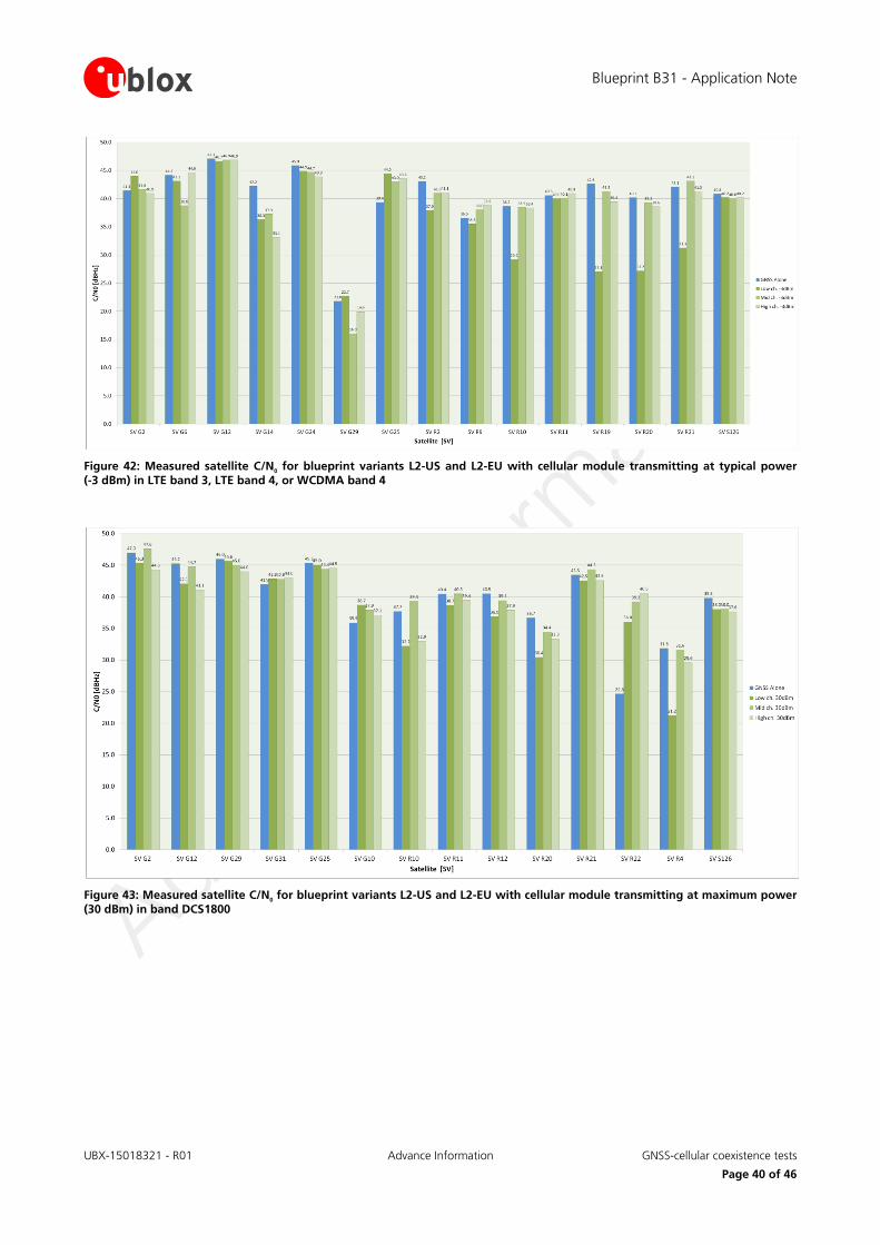
The same considerations provided for the variant L1 can be repeated here using the LTE band 4 (or WCDMA band 4). This is the only case where the test has been re-executed lowering the output power to -3 dBm (see Figure 41 and Figure 42). In all the other bands the GNSS reception is almost unaffected even with TOBY-L2 transmitting at maximum power.
As can be seen from Figure 38, Figure 40, Figure 43 and Figure 45, the GSM transmission does not degrade the GNSS reception, even though the output power is higher (33 dBm or 30 dBm) than the LTE / WCDMA case. This can be explained considering the burst nature of the GSM transmission: the signal is transmitted with a 1/8 duty cycle and this allows the positioning module to recover and correctly track all the satellite systems.
Figure 36: Measured satellite C/N0 for blueprint variants L2-US with cellular module transmitting at maximum power (23 dBm)
in LTE band 17
Figure 37: Measured satellite C/N0 for blueprint variants L2-US and L2-EU with cellular module transmitting at maximum power
(23 dBm) in LTE band 5, LTE band 20, or WCDMA band 5

Blueprint B31 - Application Note
UBX-15018321 - R01 Advance Information GNSS-cellular coexistence tests
Page 38 of 46
Figure 38: Measured satellite C/N0 for blueprint variants L2-US and L2-EU with cellular module transmitting at maximum power
(33 dBm) in band GSM850
Figure 39: Measured satellite C/N0 for blueprint variants L2-US and L2-EU with cellular module transmitting at maximum power
(23 dBm) in LTE band 8 or WCDMA band 8

Blueprint B31 - Application Note
UBX-15018321 - R01 Advance Information GNSS-cellular coexistence tests
Page 39 of 46
Figure 40: Measured satellite C/N0 for blueprint variants L2-US and L2-EU with cellular module transmitting at maximum power
(33 dBm) in band E-GSM900
Figure 41: Measured satellite C/N0 for blueprint variants L2-US and L2-EU with cellular module transmitting at maximum power
(23 dBm) in LTE band 3, LTE band 4, or WCDMA band 4
Blueprint B31 - Application Note
UBX-15018321 - R01 Advance Information GNSS-cellular coexistence tests
Page 40 of 46
Figure 42: Measured satellite C/N0 for blueprint variants L2-US and L2-EU with cellular module transmitting at typical power
(-3 dBm) in LTE band 3, LTE band 4, or WCDMA band 4
Figure 43: Measured satellite C/N0 for blueprint variants L2-US and L2-EU with cellular module transmitting at maximum power
(30 dBm) in band DCS1800
Blueprint B31 - Application Note
UBX-15018321 - R01 Advance Information GNSS-cellular coexistence tests
Page 41 of 46
Figure 44: Measured satellite C/N0 for blueprint variants L2-US and L2-EU with cellular module transmitting at maximum power
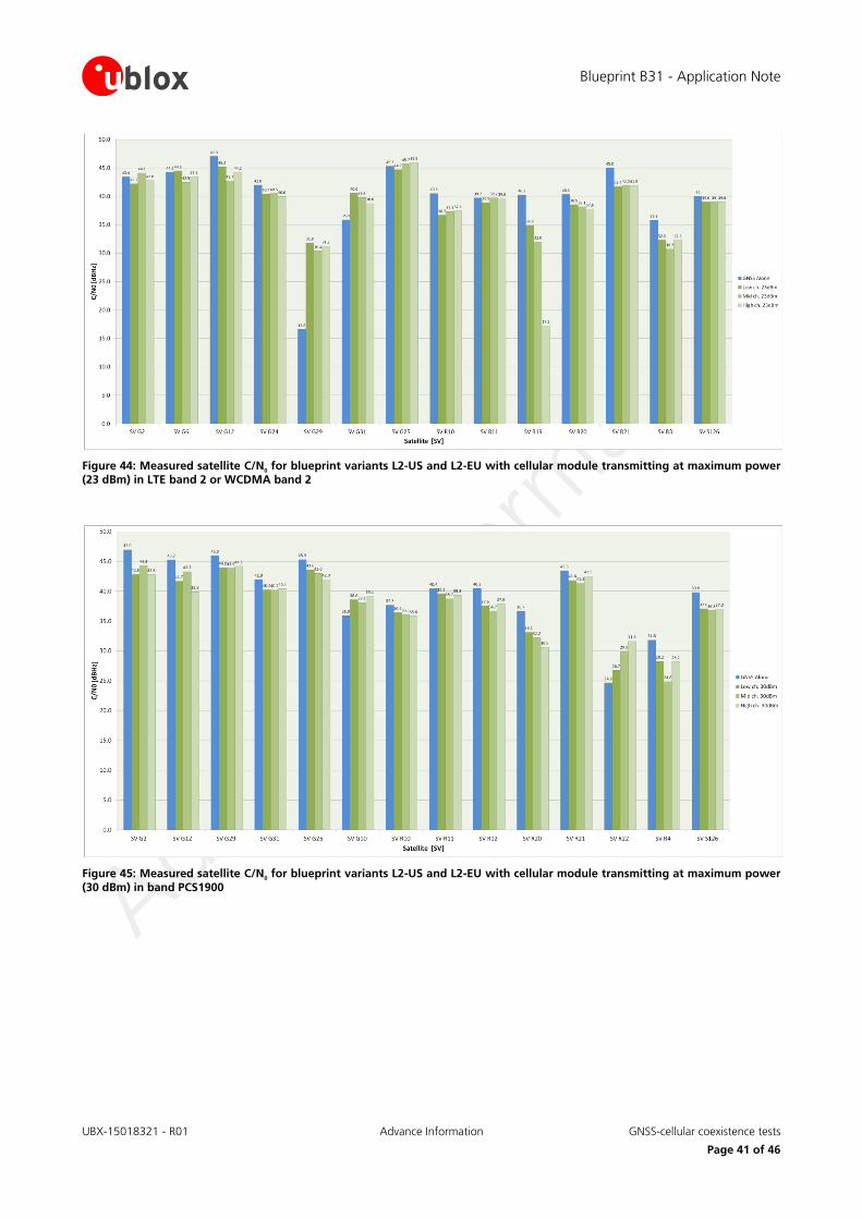
(23 dBm) in LTE band 2 or WCDMA band 2
Figure 45: Measured satellite C/N0 for blueprint variants L2-US and L2-EU with cellular module transmitting at maximum power
(30 dBm) in band PCS1900
Blueprint B31 - Application Note
UBX-15018321 - R01 Advance Information GNSS-cellular coexistence tests
Page 42 of 46
Figure 46: Measured satellite C/N0 for blueprint variants L2-US and L2-EU with cellular module transmitting at maximum power
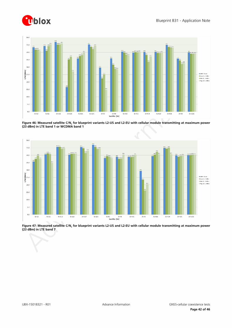
(23 dBm) in LTE band 1 or WCDMA band 1
Figure 47: Measured satellite C/N0 for blueprint variants L2-US and L2-EU with cellular module transmitting at maximum power
(23 dBm) in LTE band 7

Blueprint B31 - Application Note
UBX-15018321 - R01 Advance Information Delivered package
Page 43 of 46
7 Delivered package Blueprint B31 delivery package consists of:
Schematic files for variant L1 and variants L2-US / L2-EU (combined)
BOM files for variant L1 and variants L2-US / L2-EU (combined)
Gerber files, single file group for all the variants
Pick and Place file
Assembly files for each variant
Board Stack-up report
Blueprint B31 - Application Note
UBX-15018321 - R01 Advance Information Appendix
Page 44 of 46
Appendix
A List of acronyms Abbreviation / Term Explanation / Definition
BAW Bulk Acoustic Wave
BOM Bill Of Materials
DC Directional Current
EMI Electromagnetic Interference
FW Firmware
GNSS Global Navigation Satellite System
GPIO General Purpose Input Output
HW Hardware
I2C Inter-Integrated Circuit
LED Light Emitting Diode
LDO Low Drop-Out
LTE Long Term Evolution
OFDMA Orthogonal Frequency Division Multiple Access
OTA Over The Air
PWM Pulse Width Modulation
RF Radiofrequency
SC-FDMA Single Carrier Frequency Division Multiple Access
SDIO Secure Digital Input Output
SIM Subscriber Identification Module
UART Universal Asynchronous Receiver-Transmitter
USB Universal Serial Bus
VSWR Voltage Standing Wave Ratio
Wi-Fi IEEE 802.11 short range radio technology

Blueprint B31 - Application Note
UBX-15018321 - R01 Advance Information Related documents
Page 45 of 46
Related documents [1] u-blox TOBY-L1 / MPCI-L1 series System Integration Manual, Docu No UBX-13002211
[2] u-blox TOBY-L2 / MPCI-L2 series System Integration Manual, Docu No UBX-13004618
[3] u-blox NEO-M8 Hardware Integration Manual, Docu. No UBX-13003557
[4] u-blox ELLA-W1 series Data Sheet, Docu No UBX-15004476
[5] CTIA Test Plan for Wireless Device Over-the-Air Performance V.3.4.2
[6] 3GPP TS 51.010-1 - Technical Specification Group GSM/EDGE Radio Access Network; Mobile Station (MS) conformance specification; Part 1: Conformance specification
[7] 3GPP TS 34.124 - Universal Mobile Telecommunications System, LTE; Electromagnetic compatibility (EMC) requirements for mobile terminals and ancillary equipment
[8] 3GPP TS 36.124 - Evolved Universal Terrestrial Radio Access (E-UTRA); Electromagnetic compatibility (EMC) requirements for mobile terminals and ancillary equipment
[9] u-blox End User Test Application Note, Docu No UBX-13001922
[10] u-blox u-center User Guide, Docu No UBX-13005250
For regular updates to u-blox documentation and to receive product change notifications, register on our homepage (www.u-blox.com).
Revision history
Revision Date Name Status / Comments
R01 13-Oct-2015 sfal Initial release
Blueprint B31 - Application Note
UBX-15018321 - R01 Advance Information Contact
Page 46 of 46
Contact For complete contact information visit us at http://www.u-blox.com/
u-blox Offices
North, Central and South America
u-blox America, Inc.
Phone: +1 703 483 3180 E-mail: [email protected]
Regional Office West Coast:
Phone: +1 408 573 3640 E-mail: [email protected]
Technical Support:
Phone: +1 703 483 3185 E-mail: [email protected]
Headquarters
Europe, Middle East, Africa
u-blox AG
Phone: +41 44 722 74 44 E-mail: [email protected] Support: [email protected]
Asia, Australia, Pacific
u-blox Singapore Pte. Ltd.
Phone: +65 6734 3811 E-mail: [email protected] Support: [email protected]
Regional Office Australia:
Phone: +61 2 8448 2016 E-mail: [email protected] Support: [email protected]
Regional Office China (Beijing):
Phone: +86 10 68 133 545 E-mail: [email protected] Support: [email protected]
Regional Office China (Chongqing):
Phone: +86 23 6815 1588 E-mail: [email protected] Support: [email protected]
Regional Office China (Shanghai):
Phone: +86 21 6090 4832 E-mail: [email protected] Support: [email protected]
Regional Office China (Shenzhen):
Phone: +86 755 8627 1083 E-mail: [email protected] Support: [email protected]
Regional Office India:
Phone: +91 959 1302 450 E-mail: [email protected] Support: [email protected]
Regional Office Japan (Osaka):
Phone: +81 6 6941 3660 E-mail: [email protected] Support: [email protected]
Regional Office Japan (Tokyo):
Phone: +81 3 5775 3850 E-mail: [email protected] Support: [email protected]
Regional Office Korea:
Phone: +82 2 542 0861 E-mail: [email protected] Support: [email protected]
Regional Office Taiwan:
Phone: +886 2 2657 1090 E-mail: [email protected] Support: [email protected]