blunk electronic
TRANSCRIPT

Tutorial for Creating Device Models in CAE Tool CadSoft EAGLE
Doc. Version 201212051.3
Abstract: Tutorial for handling the EAGLE1 library to create customized device models used in the schematics and layout editor. Guideline for extracting relevant information from the datasheet all the way down to useful schematic symbols and device packages. The example used is a power supply protection IC made by Linear Technology Corp.2 the LT4356.
Keywords: datasheet, symbol, package, device, variant, technology, pin, pin direction, pad, exposed pad, smd, solder stop, pitch, layer, grid, metric, imperial, inch, mil, DFN, MSOP, SO, BGA, prototyping, prototype, thermals, thermal bridge, solder stop mask, solder cream, export, BOM, bill of material
Introduction
This document aims to give electronics design engineers a tutorial on how to create custom specific device models using the CAE tool EAGLE (version 5.x) made by the German company CadSoft Computer GmbH. Especially in the prototyping phase, engineers tight on time who are in need to get a useful PCB layout ready for production within a few days make use of this tool. The capabilities of the device library are in the scope of this tutorial using the LT4356 with its electrical and mechanical shipment options as an example.
Special thanks to Linear Technology Corporation for the LT4356 datasheet used within this document. Please visit Linear Technology Corp. at www.linear.com .
1 EAGLE is a registered trademark of CadSoft Computer GmbH.2 Linear Technology is a registered trademark of Linear Technology Corporation.
Blunk electronic at www.trainz.de 1

Contents 1 The Target Device Model...................................................................................................3
1.1 Monolithic Block Symbol.............................................................................................3 1.2 Splitting the IC Symbol................................................................................................3 1.3 Package related..........................................................................................................5 1.4 Device Code related....................................................................................................6 1.5 The LT4356 within the Library.....................................................................................7
2 Workflow.............................................................................................................................9 2.1 Creating a new empty Library...................................................................................10 2.2 Symbol Editing..........................................................................................................11
2.2.1 The MAIN symbol...............................................................................................11 2.2.2 The AMP symbol...............................................................................................12 2.2.3 Drawing the MAIN Symbols...............................................................................16
2.3 Package Editing........................................................................................................18 2.3.1 The DFN package..............................................................................................18 2.3.2 The SO package................................................................................................27 2.3.3 The MSOP package..........................................................................................29
2.4 Device Editing...........................................................................................................30 2.4.1 The DEVersion..................................................................................................30
2.4.1.1 Symbols.......................................................................................................31 2.4.1.2 Package......................................................................................................35 2.4.1.3 Connecting Symbols with Package............................................................36 2.4.1.4 Prefix...........................................................................................................38 2.4.1.5 Value...........................................................................................................38 2.4.1.6 Technologies...............................................................................................38 2.4.1.7 Attributes.....................................................................................................39
2.4.1.7.1 Company Internal Part/Device Codes..................................................41 2.4.1.8 Device Description......................................................................................42 2.4.1.9 Make the library known to EAGLE..............................................................43
2.4.2 The MSVersion.................................................................................................45 2.4.3 The SO version..................................................................................................47
2.5 Library Description....................................................................................................48 2.6 Deleting, Renaming and Copying Symbols, Packages and Devices.......................49
2.6.1 Removing...........................................................................................................49 2.6.2 Renaming..........................................................................................................50 2.6.3 Copying..............................................................................................................51
3 BOM Exporting.................................................................................................................52 4 Useful Links......................................................................................................................53 5 Disclaimer.........................................................................................................................54
2 Blunk electronic at www.trainz.de

1 The Target Device Model
1.1 Monolithic Block SymbolThe LT4356 is available with options regarding electrical characteristics, package and temperature grade. Figure 1 shows an application with the IC symbol as it would look like within the schematic editor (colored pink) if created as monolithic block. This single block is quickly to draw but lacks some flexibility.
1.2 Splitting the IC SymbolSince this is a tutorial for advanced EAGLE users, we'll split the circuit into the symbol for the main circuitry and the symbol for the auxiliary amplifier.
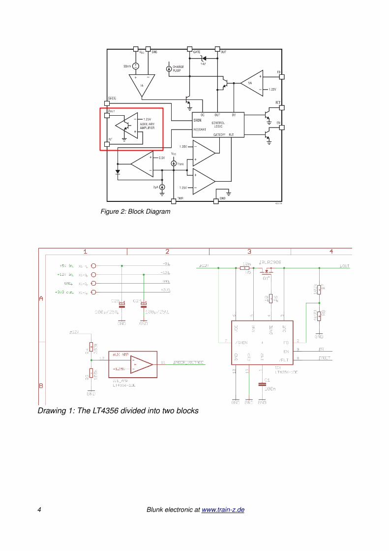
Figure 2 shows the block diagram of the IC where the auxiliary amplifier is framed red. This way the amplifier may be placed on a schematic sheet different from the one of the main symbol. When drawing schematics it is convenient to place functional blocks of a device where they are needed. Hence a schematic is easier to read. In our case the auxiliary amplifier may be placed where power is supplied e.g. next to a connector whereas the main block is located somewhere in the power output section of the schematic. See Drawing 1 as an example of what the outcome of our work is supposed to be.
Blunk electronic at www.trainz.de 3
Figure 1: Monolithic Symbol in Schematic
4 Blunk electronic at www.trainz.de
Figure 2: Block Diagram
Drawing 1: The LT4356 divided into two blocks
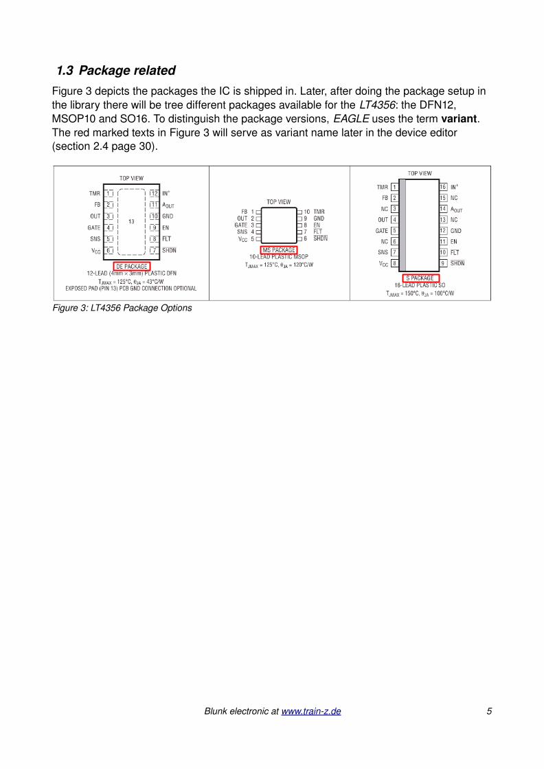
1.3 Package relatedFigure 3 depicts the packages the IC is shipped in. Later, after doing the package setup in the library there will be tree different packages available for the LT4356: the DFN12, MSOP10 and SO16. To distinguish the package versions, EAGLE uses the term variant. The red marked texts in Figure 3 will serve as variant name later in the device editor (section 2.4 page 30).
Blunk electronic at www.trainz.de 5
Figure 3: LT4356 Package Options
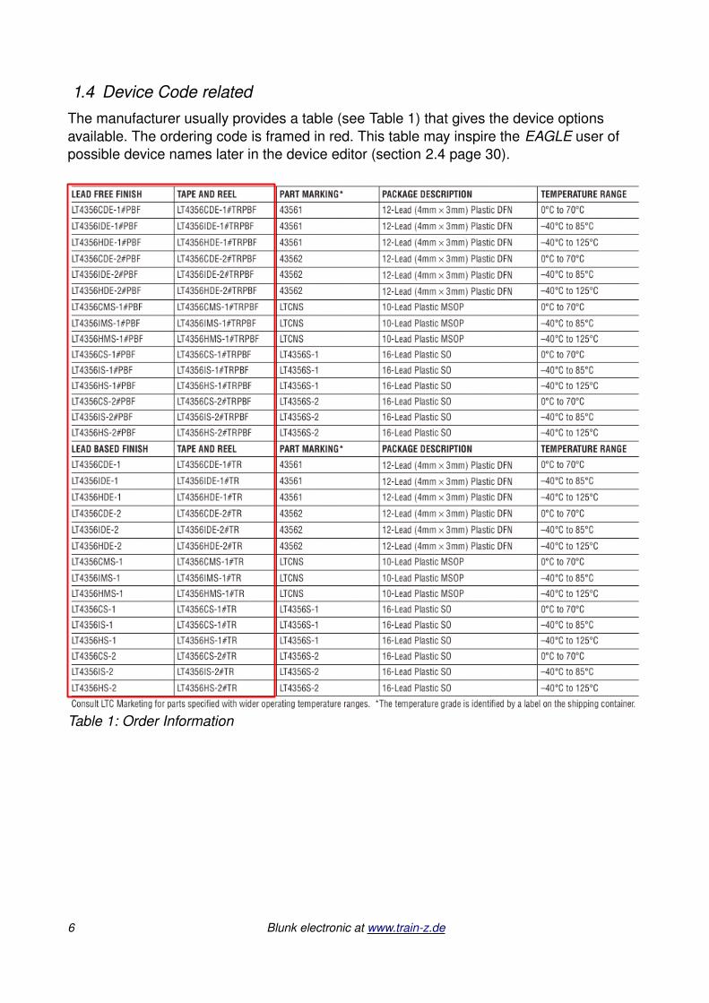
1.4 Device Code relatedThe manufacturer usually provides a table (see Table 1) that gives the device options available. The ordering code is framed in red. This table may inspire the EAGLE user of possible device names later in the device editor (section 2.4 page 30).
6 Blunk electronic at www.trainz.de
Table 1: Order Information
Example: The term LT4356CDE1 stands for the 12lead (4mm x 3mm) plastic DFN version with commercial temperature range 0°C to 70°C:
LT4356 C DE – 1 options Green temperature range→
red package →
blue electrical version→
Later the device name will be a generic term LT4356* that has a wildcard (asterisk) which stands for the electrical version #1 or #2. EAGLE uses for the electrical version the term technology. Using wildcards in the device name is not mandatory but gives flexibility.
So the electrical version – the technology – as well as the package will be coded in the device name whereas the temperature range will become an attribute (see section 2.4.1.7 page 39).
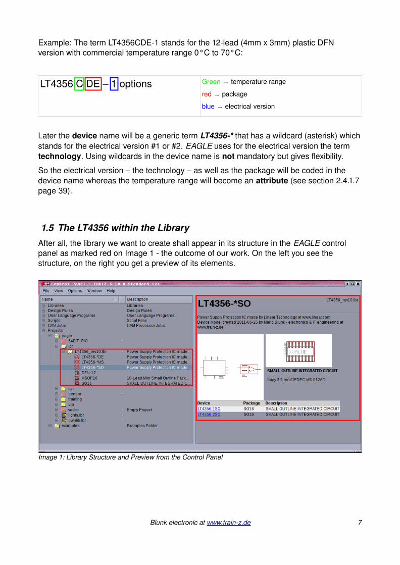
1.5 The LT4356 within the LibraryAfter all, the library we want to create shall appear in its structure in the EAGLE control panel as marked red on Image 1 the outcome of our work. On the left you see the structure, on the right you get a preview of its elements.
Blunk electronic at www.trainz.de 7
Image 1: Library Structure and Preview from the Control Panel
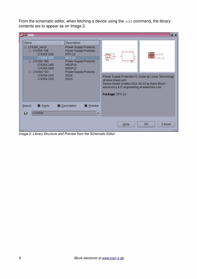
From the schematic editor, when fetching a device using the add command, the library contents are to appear as on Image 2.
8 Blunk electronic at www.trainz.de
Image 2: Library Structure and Preview from the Schematic Editor
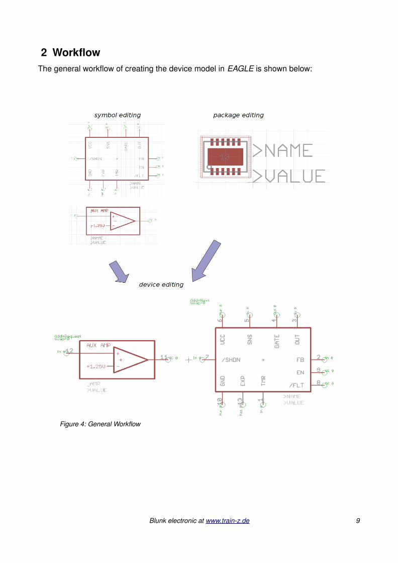
2 WorkflowThe general workflow of creating the device model in EAGLE is shown below:
Blunk electronic at www.trainz.de 9
Figure 4: General Workflow
Some general rules apply:
1. The connection of symbol(s) and package(s) makes a device.
Note Figure 4: after device editing, pin numbers appear next to the symbol pins.
2. The device name usually gets an extension automatically that tells the package variant.
3. Symbols in general don't say anything about technology or packages3.
4. Several symbols may belong to a device (in our case main and amplifier symbol).
5. Several packages may belong to a device (in our case DFN12, MSOP10, SO16).
6. The library model is ready for use in schematic and PCB layout when symbol(s) and at least one package have been joined to a device.
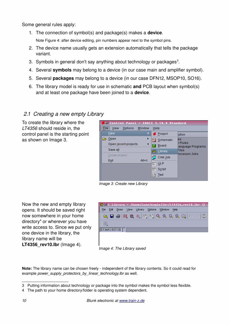
2.1 Creating a new empty LibraryTo create the library where the LT4356 should reside in, the control panel is the starting point as shown on Image 3.
Now the new and empty library opens. It should be saved right now somewhere in your home directory4 or wherever you have write access to. Since we put only one device in the library, the library name will be LT4356_rev10.lbr (Image 4).
Note: The library name can be chosen freely independent of the library contents. So it could read for example power_supply_protectors_by_linear_technology.lbr as well.
3 Putting information about technology or package into the symbol makes the symbol less flexible.4 The path to your home directory/folder is operating system dependent.
10 Blunk electronic at www.trainz.de
Image 3: Create new Library
Image 4: The Library saved

2.2 Symbol EditingCreating the symbol is usually the first step. The symbol defines the appearance of the IC within the schematic.
The usual question at this stage is whether to take existing symbols from another library or to draw new ones from scratch. However, the skills needed to modify an existing symbol are the same as for drawing a new one. Since the LT4356 symbols are very simple we choose the latter option.
Click on the symbol icon marked in red on Image 5.
2.2.1 The MAIN symbol
Now you are asked for the symbol name. We need several symbols remember one for the main circuitry and one of the auxiliary amplifier.
We create the main symbol first and name it LT4356_MAIN+EXP as shown on Image 6.
Don't get confused by the buttons Dev, Pac and Sym. They are a leftover from the old times of EAGLE :) Just click on OK.
In case you need to delete or rename the symbol see section 2.6 page 49.
Say yes to this warning shown right hand.
Blunk electronic at www.trainz.de 11
Image 5: Edit a Symbol
Image 7: Confirm new Symbol
Image 6: Name the Symbol
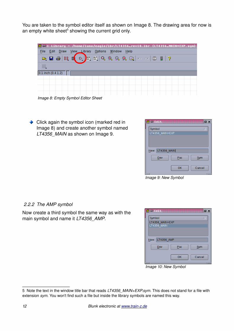
You are taken to the symbol editor itself as shown on Image 8. The drawing area for now is an empty white sheet5 showing the current grid only.
Click again the symbol icon (marked red in Image 8) and create another symbol named LT4356_MAIN as shown on Image 9.
2.2.2 The AMP symbol
Now create a third symbol the same way as with the main symbol and name it LT4356_AMP.
5 Note the text in the window title bar that reads LT4356_MAIN+EXP.sym. This does not stand for a file with extension sym. You won't find such a file but inside the library symbols are named this way.
12 Blunk electronic at www.trainz.de
Image 8: Empty Symbol Editor Sheet
Image 10: New Symbol
Image 9: New Symbol

Now that we are here in the symbol editor for the LT4356_AMP symbol we proceed with drawing this fairly simple symbol:
First type the command wire or click the wire button6.
Change line width to 0,016 inch.
Draw the amplifier body in layer 94 (symbol layer): a rectangular box with an opamp inside as shown on Image 11. Don't change the grid that defaults to 0,1 inch.
Based on this grid, the amplifier body should be 0,6 inch high and 1,1 inch wide.
Thinner “wires” going into and out of the opamp need to be added with the wire command still active. Please change the line with to 0,006 inch (Image 12).
The amp pins should be placed next using the command pin (or click the button in the toolbar).
Once the pinmode is active, the pin properties may be set like pin orientation, length, I/O characteristics, visibility. The latter should be set by click on the property button framed in red on Image 13. This way the pin name will not be shown in the schematic later on, whereas the pad number is visible.
6 Although the term wire resembles an electrical wire, “wire” here means all kinds of lines in whatever layer.
Blunk electronic at www.trainz.de 13
Image 11: Amplifier Body
Image 12: Amplifier Body
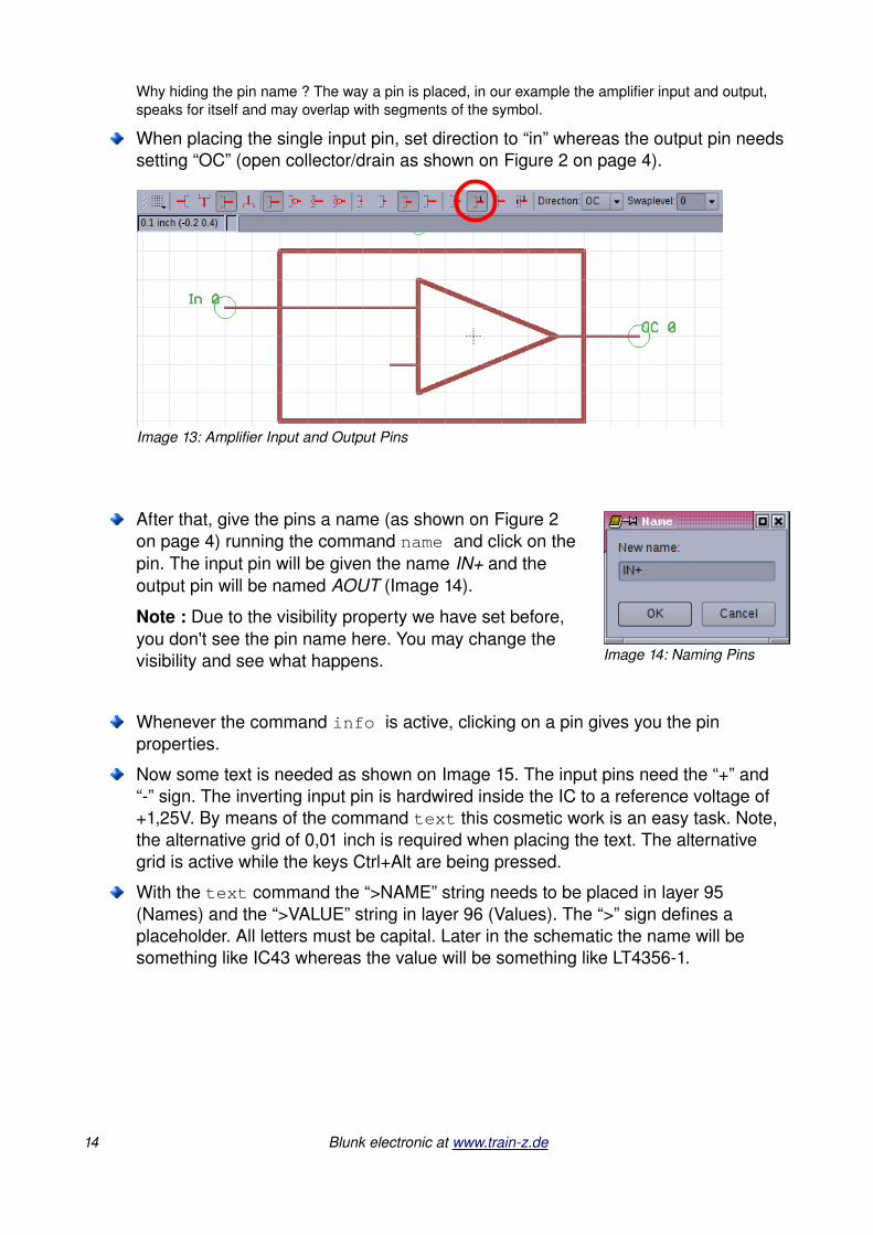
Why hiding the pin name ? The way a pin is placed, in our example the amplifier input and output, speaks for itself and may overlap with segments of the symbol.
When placing the single input pin, set direction to “in” whereas the output pin needs setting “OC” (open collector/drain as shown on Figure 2 on page 4).
After that, give the pins a name (as shown on Figure 2 on page 4) running the command name and click on the pin. The input pin will be given the name IN+ and the output pin will be named AOUT (Image 14).
Note : Due to the visibility property we have set before, you don't see the pin name here. You may change the visibility and see what happens.
Whenever the command info is active, clicking on a pin gives you the pin properties.
Now some text is needed as shown on Image 15. The input pins need the “+” and “” sign. The inverting input pin is hardwired inside the IC to a reference voltage of +1,25V. By means of the command text this cosmetic work is an easy task. Note, the alternative grid of 0,01 inch is required when placing the text. The alternative grid is active while the keys Ctrl+Alt are being pressed.
With the text command the “>NAME” string needs to be placed in layer 95 (Names) and the “>VALUE” string in layer 96 (Values). The “>” sign defines a placeholder. All letters must be capital. Later in the schematic the name will be something like IC43 whereas the value will be something like LT43561.
14 Blunk electronic at www.trainz.de
Image 13: Amplifier Input and Output Pins
Image 14: Naming Pins

For all text labels I recommend vector font text size 0,05 inch and a ratio of 8%. 8% ratio means 8% of 0,05 inch that yields 4 mil or 0,1mm line width).→
Save the library and we are done with the first symbol.
Blunk electronic at www.trainz.de 15
Image 15: Placing Text Labels
2.2.3 Drawing the MAIN Symbols
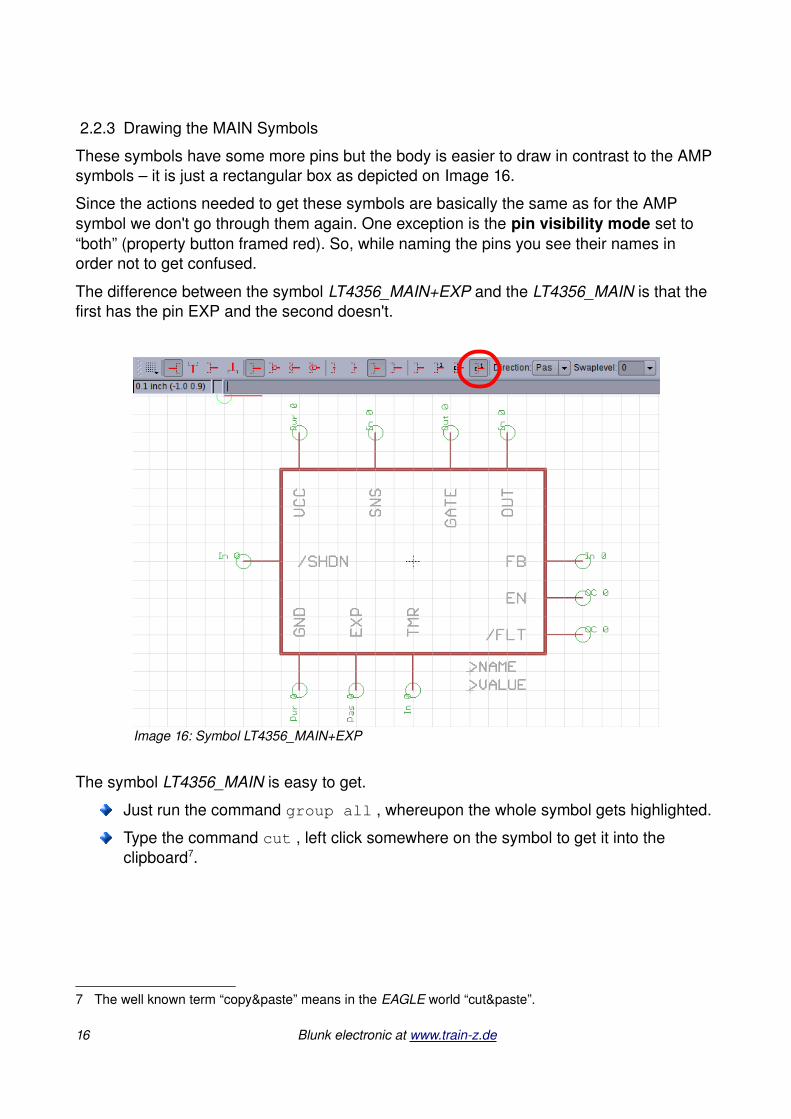
These symbols have some more pins but the body is easier to draw in contrast to the AMP symbols – it is just a rectangular box as depicted on Image 16.
Since the actions needed to get these symbols are basically the same as for the AMP symbol we don't go through them again. One exception is the pin visibility mode set to “both” (property button framed red). So, while naming the pins you see their names in order not to get confused.
The difference between the symbol LT4356_MAIN+EXP and the LT4356_MAIN is that the first has the pin EXP and the second doesn't.
The symbol LT4356_MAIN is easy to get.
Just run the command group all , whereupon the whole symbol gets highlighted.
Type the command cut , left click somewhere on the symbol to get it into the clipboard7.
7 The well known term “copy&paste” means in the EAGLE world “cut&paste”.
16 Blunk electronic at www.trainz.de
Image 16: Symbol LT4356_MAIN+EXP

Now click the symbol icon as marked red on Image 17.
Select the symbol LT4356_MAIN from the box that comes up then (Image 18).
The symbol editor opens with an empty sheet. Run the command paste . The LT4356_MAIN+EXP symbol should be attached to your cursor now. Place it so that the origin is right in its center. So far it looks exactly as in Image 16.
Run the command delete and left click the EXP pin. The result should look as on Image 19.
Blunk electronic at www.trainz.de 17
Image 17: Open Symbol
Image 18: Select Symbol
Image 19: Symbol LT4356_MAIN
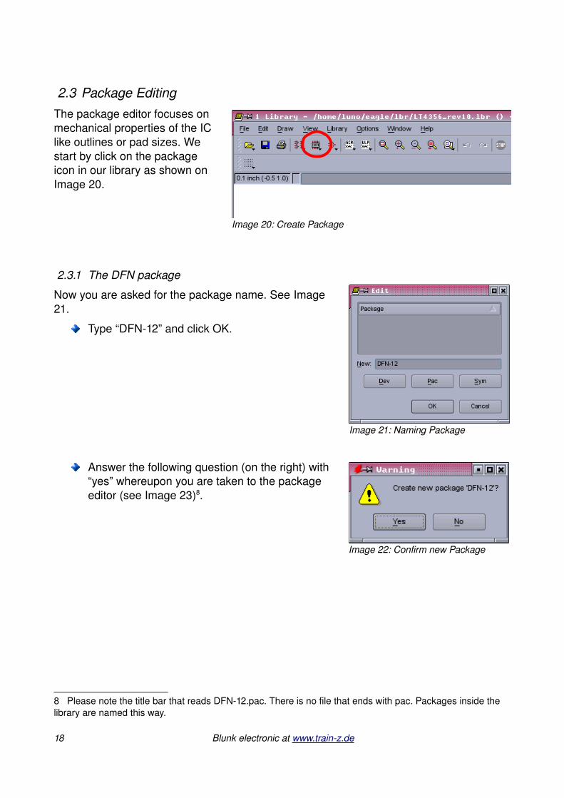
2.3 Package EditingThe package editor focuses on mechanical properties of the IC like outlines or pad sizes. We start by click on the package icon in our library as shown on Image 20.
2.3.1 The DFN package
Now you are asked for the package name. See Image 21.
Type “DFN12” and click OK.
Answer the following question (on the right) with “yes” whereupon you are taken to the package editor (see Image 23)8.
8 Please note the title bar that reads DFN12.pac. There is no file that ends with pac. Packages inside the library are named this way.
18 Blunk electronic at www.trainz.de
Image 20: Create Package
Image 21: Naming Package
Image 22: Confirm new Package

Since most packages are standardized and already drawn in other libraries the packages DFN12, MSOP10 and SO16 we need for the LT4356 may be copied into our library by drag and drop. Modifying a package requires the same skills as creating one from scratch. So a good training object is to redraw the DFN package shown in Figure 5 on page 20.
A basically important point to mention is note 3 in Figure 5 (marked with a red arrow). Hence the working grid should be set to metric 1,5mm. 1,5mm due to the IC housing outline of 3x4mm which we will draw first.
By typing the command grid (or clicking on the gridbutton) a box opens where you enter the grid we need now. Please also enter the alternative grid of 0,1mm for fine tunings (Image 24).
Blunk electronic at www.trainz.de 19
Image 23:
Image 24: Metrical Grid Settings


Back in the editor window type the command wire and draw the IC housing a 3x4mm box in layer 21 (tPlace) around the origin (marked with a red arrow). Use line with of 0,127mm (which equals 5 mil in imperial system) as shown below on Image 25.
The pin 1 top mark can be drawn using the command circle. Once this command is active, click where the circle center is supposed to be, then press Ctrl+Alt key simultaneously and click again where the circle outline should be. The outcome of your actions should look as shown on Image 25.
Next we add the SMD pads with the command smd. The information of pad sizes and where to place them is provided by the red framed part of Figure 5. As soon as the smd command is in action a pad is attached already on the cursor. Just place it somewhere next to the housing as shown on Image 26.
Change the grid to 0.25mm.
Blunk electronic at www.trainz.de 21
Image 25: Drawing the IC housing
Image 26: Placing a Pad
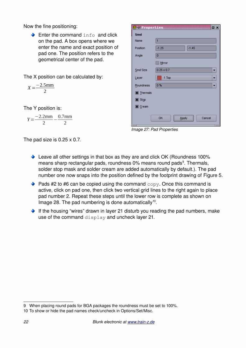
Now the fine positioning:
Enter the command info and click on the pad. A box opens where we enter the name and exact position of pad one. The position refers to the geometrical center of the pad.
The X position can be calculated by:
X =−2.5mm
2
The Y position is:
Y=−2.2mm
2−
0.7mm2
The pad size is 0.25 x 0.7.
Leave all other settings in that box as they are and click OK (Roundness 100% means sharp rectangular pads, roundness 0% means round pads9. Thermals, solder stop mask and solder cream are added automatically by default.). The pad number one now snaps into the position defined by the footprint drawing of Figure 5.
Pads #2 to #6 can be copied using the command copy. Once this command is active, click on pad one, then click two vertical grid lines to the right again to place pad number 2. Repeat these steps until the lower row is complete as shown on Image 28. The pad numbering is done automatically10.
If the housing “wires” drawn in layer 21 disturb you reading the pad numbers, make use of the command display and uncheck layer 21.
9 When placing round pads for BGA packages the roundness must be set to 100%.10 To show or hide the pad names check/uncheck in Options/Set/Misc.
22 Blunk electronic at www.trainz.de
Image 27: Pad Properties
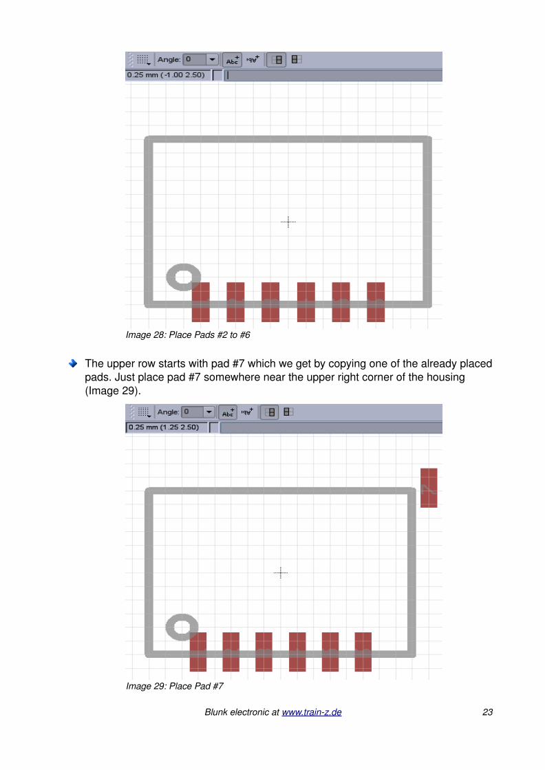
The upper row starts with pad #7 which we get by copying one of the already placed pads. Just place pad #7 somewhere near the upper right corner of the housing (Image 29).
Blunk electronic at www.trainz.de 23
Image 29: Place Pad #7
Image 28: Place Pads #2 to #6

Again fine positioning:
Enter the command info and click on pad #7. Enter the exact position of the pad.
The X position can be calculated by:
X =2.5mm
2
The Y position is:
Y =2.2mm
2
0.7mm2
Once applied the pad #7 moves to that position.
By copying pad by pad the upper row can be completed easily. So your work should look as shown on Image 31.
One last pad needs to be placed: Pad 13 covers most of the area between the upper and lower pad rows. The datasheet refers to it as the Exposed Pad.
24 Blunk electronic at www.trainz.de
Image 30: Pad Properties
Image 31: Place Pads #7 to #12

Enter command smd and place a huge pad as shown in Image 32. Using the command info the name 13 is to be given.
In order to avoid the package placed to close to other SMD components a kind of “safety frame” should be drawn around the package11 in layer 39 (tKeepout)12.
Use the command wire and a line with of 0,2mm and draw a rectangular box around as shown on Image 33.
The DRC (Design Rule Check) applied to the PCB layout later on checks for overlaps of these “safety frames”.
11 In general I also recommend this measure for THT packages.12 Don't care about the bottom layer. They layout editor “mirrors” layer 39 to layer 40 automatically when
placing packages on the bottom side of the board.
Blunk electronic at www.trainz.de 25
Image 32: Placing the EXP Pad #13
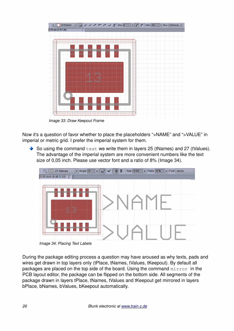
Now it's a question of favor whether to place the placeholders “>NAME” and “>VALUE” in imperial or metric grid. I prefer the imperial system for them.
So using the command text we write them in layers 25 (tNames) and 27 (tValues). The advantage of the imperial system are more convenient numbers like the text size of 0,05 inch. Please use vector font and a ratio of 8% (Image 34).
During the package editing process a question may have aroused as why texts, pads and wires get drawn in top layers only (tPlace, tNames, tValues, tKeepout). By default all packages are placed on the top side of the board. Using the command mirror in the PCB layout editor, the package can be flipped on the bottom side. All segments of the package drawn in layers tPlace, tNames, tValues and tKeepout get mirrored in layers bPlace, bNames, bValues, bKeepout automatically.
26 Blunk electronic at www.trainz.de
Image 33: Draw Keepout Frame
Image 34: Placing Text Labels

2.3.2 The SO package
The LT4356 is also available in the SO16 package (see Figure 6). It is widely used by semiconductor manufacturers. So there is no need to draw one from scratch. However, to improve the user skills, drawing one anew is a good training object.
Blunk electronic at www.trainz.de 27
Figure 6: S Drawing
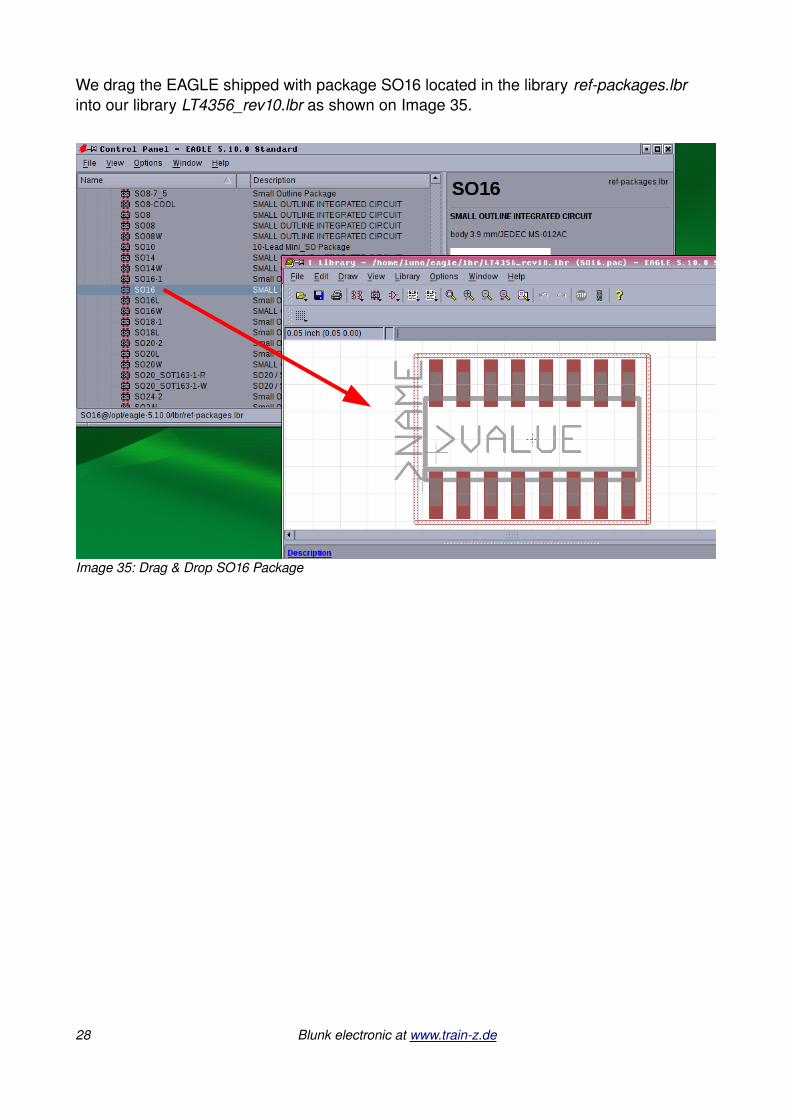
We drag the EAGLE shipped with package SO16 located in the library refpackages.lbr into our library LT4356_rev10.lbr as shown on Image 35.
28 Blunk electronic at www.trainz.de
Image 35: Drag & Drop SO16 Package
2.3.3 The MSOP package
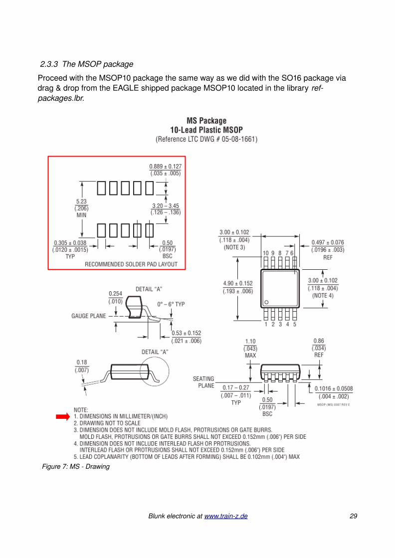
Proceed with the MSOP10 package the same way as we did with the SO16 package via drag & drop from the EAGLE shipped package MSOP10 located in the library refpackages.lbr.
Blunk electronic at www.trainz.de 29
Figure 7: MS Drawing
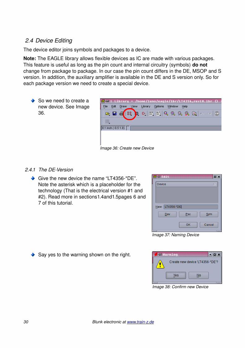
2.4 Device EditingThe device editor joins symbols and packages to a device.
Note: The EAGLE library allows flexible devices as IC are made with various packages. This feature is useful as long as the pin count and internal circuitry (symbols) do not change from package to package. In our case the pin count differs in the DE, MSOP and S version. In addition, the auxiliary amplifier is available in the DE and S version only. So for each package version we need to create a special device.
So we need to create a new device. See Image 36.
2.4.1 The DEVersion
Give the new device the name “LT4356*DE”. Note the asterisk which is a placeholder for the technology (That is the electrical version #1 and #2). Read more in sections1.4and1.5pages 6 and 7 of this tutorial.
Say yes to the warning shown on the right.
30 Blunk electronic at www.trainz.de
Image 36: Create new Device
Image 38: Confirm new Device
Image 37: Naming Device

Now you are taken to the device editor as shown on Image 3913.
2.4.1.1 Symbols
First we'll fetch the symbols needed for the device.
Type the command add and a box opens where you are asked which symbol of the currently opened library to fetch (Image 40).
So select the LT4356_AMP symbol and click OK.
13 Note the title bar that reads LT4356*DE.dev. You won't find a file like this. Devices are named inside a library this way.
Blunk electronic at www.trainz.de 31
Image 39: Device Editor
Image 40: Fetch Symbol
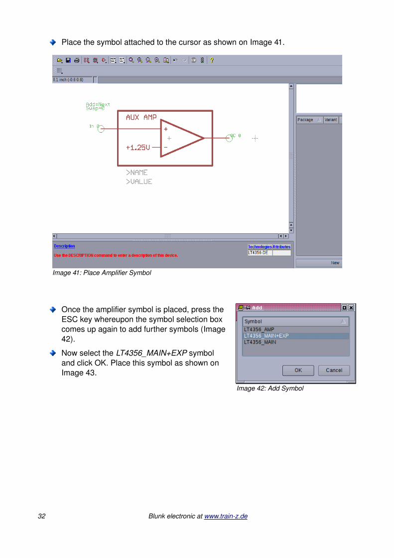
Place the symbol attached to the cursor as shown on Image 41.
Once the amplifier symbol is placed, press the ESC key whereupon the symbol selection box comes up again to add further symbols (Image42).
Now select the LT4356_MAIN+EXP symbol and click OK. Place this symbol as shown on Image 43.
32 Blunk electronic at www.trainz.de
Image 41: Place Amplifier Symbol
Image 42: Add Symbol
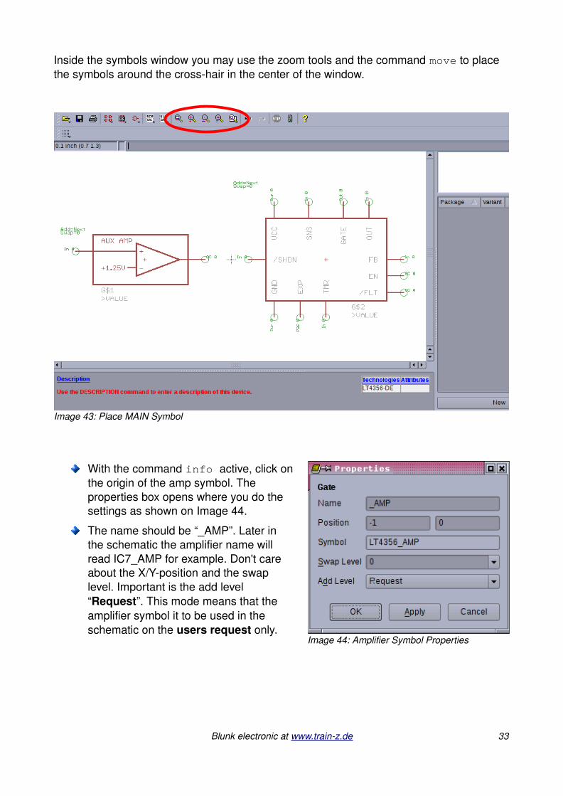
Inside the symbols window you may use the zoom tools and the command move to place the symbols around the crosshair in the center of the window.
With the command info active, click on the origin of the amp symbol. The properties box opens where you do the settings as shown on Image 44.
The name should be “_AMP”. Later in the schematic the amplifier name will read IC7_AMP for example. Don't care about the X/Yposition and the swap level. Important is the add level “Request”. This mode means that the amplifier symbol it to be used in the schematic on the users request only.
Blunk electronic at www.trainz.de 33
Image 43: Place MAIN Symbol
Image 44: Amplifier Symbol Properties

Now that the info command is still active, click on the main symbol and enter the properties as shown in Image 45. Don't care about the positioning but care for the add level “Next”.
Note: If you discover a mistake in one of the symbols you can go back to the symbol editor any time and iron it out. Symbols already added to the device editor get updated automatically.
Finally the symbols in the device editor should look as on Image 46.
34 Blunk electronic at www.trainz.de
Image 45: Main Symbol Properties
Image 46: Symbols added

2.4.1.2 Package
The symbol assembly we have ready now fits into the DFN12 package only.
Type the command pac, a box opens where you select the package to add. In this example, select package “DFN12” and click OK.
Note: Don't enter a name for this device variant. We've already “hard coded” the package variant name in the device name (see title bar on Image 47). The reason for hard coding the package variant in the device name is that the symbol assembly we have done above is available in the DE version only. In detail: The symbol LT4356_MAIN+EXP has the exposed pin which exists in the DE version only.
By the way the MSOP10 package is visible in the list but can't be added since its pin count (10) is less than the total pin count (13) of our symbol assembly (see Image 46).
Further on, despite the SO16 package can be fetched because of its pin count, it does not have the EXP pin. When it comes to connecting symbols and package later on (section 2.4.1.3 page 36), the EXP pin could be ignored. For a quick and dirty approach this could be acceptable.
Click OK and the DFN12 package appears on the right of the device editor (Image 48). By not giving a variant name on Image 47 the quotation mark (“) now stands for the “nonexistingvariant”. If a variant name was given, it would be there instead of the quotation.
Blunk electronic at www.trainz.de 35
Image 47: Select Package DFN12

2.4.1.3 Connecting Symbols with Package
Now an important step of your work is to come.
Click the “connect” button (Image 49).
36 Blunk electronic at www.trainz.de
Image 49: Connecting Symbols and Package
Image 48: Package selected
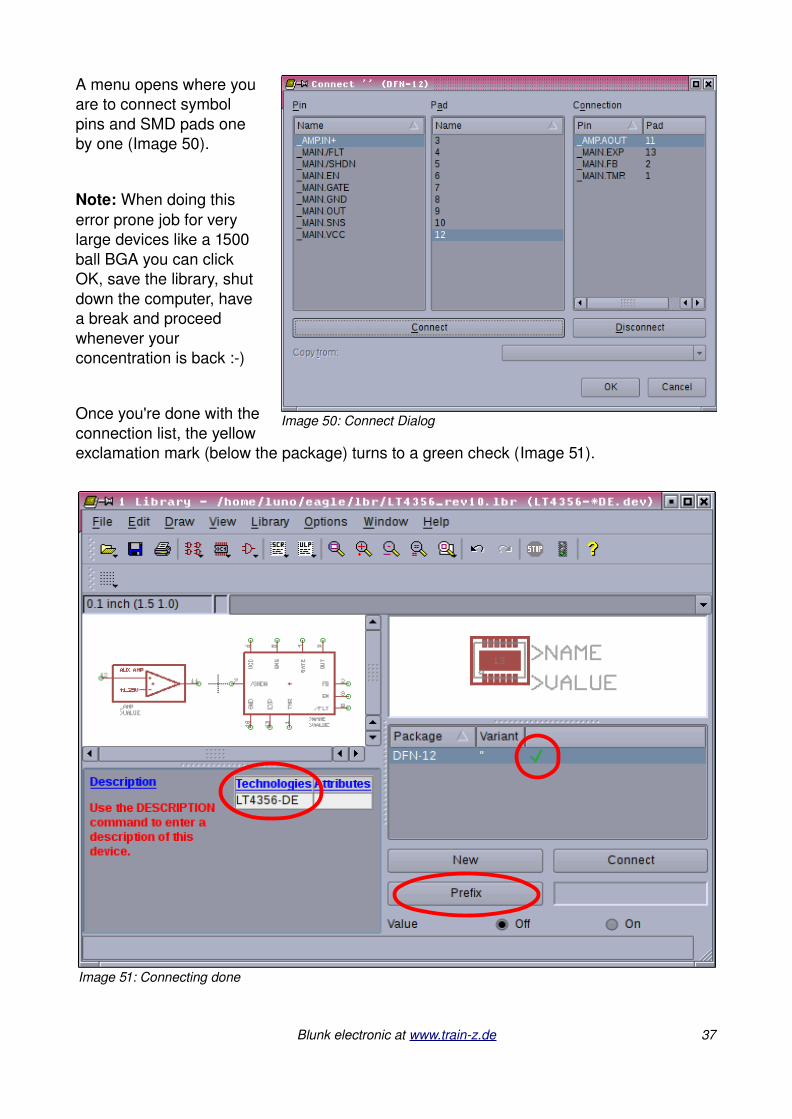
A menu opens where you are to connect symbol pins and SMD pads one by one (Image 50).
Note: When doing this error prone job for very large devices like a 1500 ball BGA you can click OK, save the library, shut down the computer, have a break and proceed whenever your concentration is back :)
Once you're done with the connection list, the yellow exclamation mark (below the package) turns to a green check (Image 51).
Blunk electronic at www.trainz.de 37
Image 50: Connect Dialog
Image 51: Connecting done

2.4.1.4 Prefix
Later in the schematic the LT4356 should have a name like IC34 or V1701. Click on the prefix button (framed red on Image 51). Enter your preferred prefix here and click OK.
2.4.1.5 Value
It is unlikely that the value of the device needs to be changed later in the schematic. So leave the Value setting as it is on “off” (see Image 51 lower right corner).
2.4.1.6 Technologies
Independent of package or symbols the LT4356 is manufactured in electrical version #1 and #2. This one digit number has already been cared for by the asterisk (the * character) in the device name LT4356*DE.
Click the blue printed word “Technologies” (framed red on Image 51).
A box opens that asks for the technology name. Type a “1” in the NewField and uncheck the default technology as shown on Image 53.
Click OK and create technology “2” as shown in Image 54.
Click OK to accept this technology.
Exit that box by another click on OK.
38 Blunk electronic at www.trainz.de
Image 52: Set Prefix
Image 53: Define Technology 1
Image 54: Define Technology 2

The technologies overview in your device editor should look as depicted on Image 55 showing the LT43561DE and the LT43562DE.
Note the asterisk has been replaced automatically by the numbers 1 and 2 respectively.
2.4.1.7 Attributes
A look at table Table 1 on page 6 immediately makes clear that lots of further information is needed to exactly specify the LT4356 like temperature range, lead free or tape&reel shipment. Therefore the attributes tool is made for.
Click the blue word “Attributes” framed red on Image 55.
The attributes editor box opens where for each technology attributes can be defined.
Let's take the temperature range for example.
Click “New” and fill the next box as shown on Image 57. Since the primary objective of the LT4356 are (peaceful) avionics applications the military range is our default value. Both technologies #1 and #2 are available for commercial and industrial temperature range as well. So the value shall not be fixed but variable.
Blunk electronic at www.trainz.de 39
Image 55: Technologies defined
Image 56: Attributes Editor
Image 57: New Attribute
Now click OK and you are taken back to the attributes overview that should look as on Image 58 now.
Let's assume there are no more attributes to add.
Click OK and have a look at the device editor that shows the attributes defined so far (Image 59).
You may save the library as it is now, close EAGLE down and have a break. Further attributes can be specified any time by click on the blue word “Attributes”.
Reasoning from Table 1 on page 6 the kind of finish and the tape&reel option should be added the same way as the temperature range as shown on Image 60.
An idea is to use the attributes to define a preferred distributor for the device and the order code for that vendor. So all information is handy to order the device quickly or trace down the supply chain.
40 Blunk electronic at www.trainz.de
Image 58: Attribute “Temperature Range” defined
Image 59: Back in the Device Editor
Image 60: Further Attributes defined

2.4.1.7.1 Company Internal Part/Device Codes
It is common for companies to have their internal part or device code that applies only for that facility.
So click on “Attributes” and fill the box as shown on Image 61 and set the imaginary value “NCC1701D” to constant. It is a constant because within your company the device LT43561, DE package, lead free, tape&reel and military temperature range is registered as NCC1701D.
Click OK and see what happens in the attributes overview (Image 62). The newly defined device code appears only in the technology “1” line.
Now click the empty field right below the 1device code (framed red on Image 62) followed by a click on the “Change” button.
Enter the device code for version “2” in the box that comes up now (Image 63). Call it NCC1701E for example and make it a constant too.
By click on OK you get back to the attributes overview window. There click on OK also and you're back in the device editor.
Blunk electronic at www.trainz.de 41
Image 61: Internal Code 1
Image 62: Change Internal Code
Image 63: Internal Code 2

Your technologies and attributes should look as shown on Image 64.
2.4.1.8 Device Description
Finally your device needs some explanation of who created the model and its creation time.
Run the command desc or click the blue word “Description” left hand of the technologies and attributes overview (see Image 59 page 40). A box opens where you can type some text as shown on Image 65.
Note: Since this text is HTML by nature, the line break (or carriage return) must be written as “<br>”. Just pressing ENTER does not work.
42 Blunk electronic at www.trainz.de
Image 64: Attributes done
Image 65: Device Description
2.4.1.9 Make the library known to EAGLE
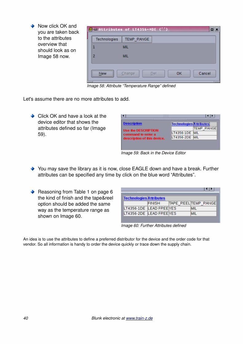
Your device editor window as a whole should look as Image 66.
Now the LT4356*DE device is ready for use in the schematic and PCB layout !
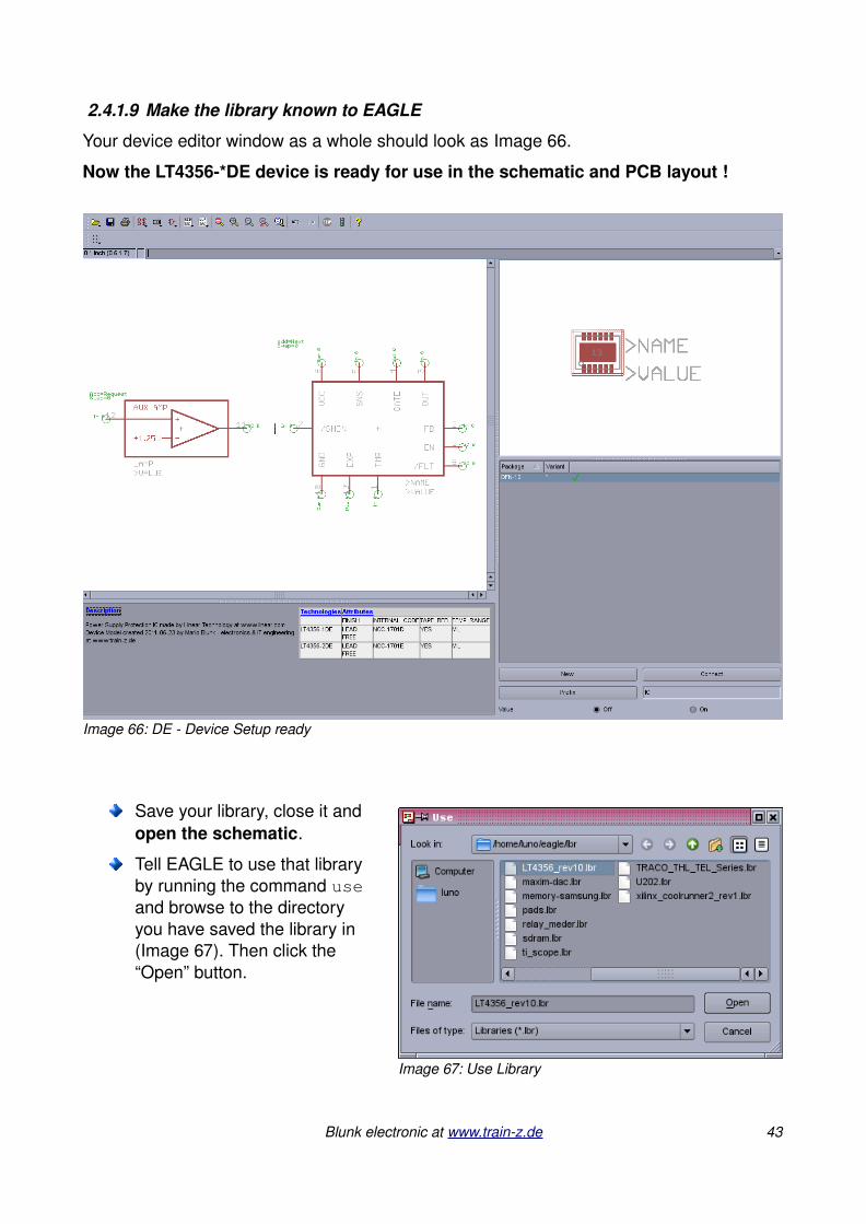
Save your library, close it and open the schematic.
Tell EAGLE to use that library by running the command use and browse to the directory you have saved the library in (Image 67). Then click the “Open” button.
Blunk electronic at www.trainz.de 43
Image 66: DE Device Setup ready
Image 67: Use Library

Now you can place the LT4356*DE in your schematic using the command add or the corresponding button in the tool bar.
If everything went correct, the preview the add command gives, should look as on Image 68. You see the LT4356 version #1 and #2 in DE package !
Select the version you need and click OK. The LT4356 MAIN symbol is attached to the cursor.
Place it in your schematic.
In my example here it has gotten the name IC7. Because the AMP symbol is not mandatory it can be fetched any time from the library into the current schematic sheet using for example the command invoke IC7.
44 Blunk electronic at www.trainz.de
Image 68: Preview when adding the Device

Select the AMP symbol from the box that comes up, click OK and put the AMP symbol down where you need it on the current schematic page (Image 69).
The AMP symbol automatically gets the same name as the MAIN symbol plus an appendix “_AMP” (Image 70). Remember the step when the symbols got named in section 2.4.1.1.
2.4.2 The MSVersion
The LT4356 is manufactured with MSOP10 package lacking the auxiliary amplifier. We need to create a device, lets name it LT4356*MS, that incorporates only the MAIN symbol without the EXP pin.
Remember, the asterisk holds place for the technology #1 or #2. The EXP pin does not exist on the MSOP10 package (see Figure 3 page 5).
Blunk electronic at www.trainz.de 45
Image 69: Invoke the AMP Symbol
Image 70: The AMP Symbol placed

The following steps are described less detailed since we went through the basics already.
Create another device LT4356*MS (Image 71).
Fetch and place the LT4356_MAIN symbol using the command add and name it MAIN.
Fetch the MSOP10 package with command pac.
Note: You won't need other packages like the DFN12 or the SO16 because the LT4356 version without auxiliary amplifier exists in the MSOP10 package only.
Connect symbol and package pins (command connect or the “Connect” button).
Set the prefix to “IC”.
Define Technologies and Attributes.
Save the library.
Your work should look as shown on Image 72.
46 Blunk electronic at www.trainz.de
Image 71: Create second Device
Image 72: MS Device Setup ready

2.4.3 The SO version
The SO version of the LT4356 does have the auxiliary amplifier built in but does not have the EXP pin.
So create a third device and name it LT4356*SO. This device is to be assembled with the symbols LT4356_MAIN and LT4356_AMP. You need the SO16 package only for this version (see Image 73).
Blunk electronic at www.trainz.de 47
Image 73: S Device Setup ready

2.5 Library DescriptionA last action to document your work it's always recommended to leave a few lines that describe the library as a whole.
Since the library LT4356_rev10.lbr is solely made for the LT4356 the description is the same as for the devices.
So go to menu Library/Description as marked on Image 74 and paste the text we used when describing the devices in the description box next (Image 75).
48 Blunk electronic at www.trainz.de
Image 74: Library Description
Image 75: Library Description done

2.6 Deleting, Renaming and Copying Symbols, Packages and DevicesThere will be situations when an erroneously created symbol, package or device needs to be deleted or renamed.
2.6.1 Removing
Go to the menu Library/Remove as marked red on Image 76.
Type the element you like to remove in the box that comes up. You need to know the exact name of the symbol, package or device as there is no pulldown menu to select.
Don't forget the extension like sym, pac or dev (Image 77) !
Note: A symbol or package already used by a device can not be removed !
Blunk electronic at www.trainz.de 49
Important:
Within the library there is no menu function like “Save Symbol as ...” !
The saveas function in the menu “File/Save as ...” applies for the whole library file (with
all its symbols, packages and devices) like your LT4356_rev10.lbr !
Image 76: Remove Elements
Image 77: Remove Device
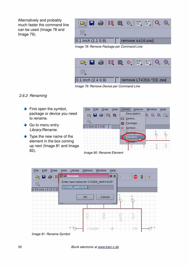
Alternatively and probably much faster the command line can be used (Image 78 and Image 79).
2.6.2 Renaming
First open the symbol, package or device you need to rename.
Go to menu entry Library/Rename.
Type the new name of the element in the box coming up next (Image 81 and Image82).
50 Blunk electronic at www.trainz.de
Image 78: Remove Package per Command Line
Image 79: Remove Device per Command Line
Image 81: Rename Symbol
Image 80: Rename Element

2.6.3 Copying
Unfortunately there is no direct way to copy a symbol, package or device directly within the same library. Instead the familiar succession of the commands group all, cut and paste is to be applied.
Remember in section 2.2.3page 16 we did this when creating the symbol LT4356_MAIN. This method also works when copying from one library to another.
Blunk electronic at www.trainz.de 51
Image 82: Rename Device

3 BOM ExportingBy default EAGLE does not export attributes into the BOM (Bill of Material) via the menu entry File/Export/Partlist .
Instead download the ULP (User Language Program) bom_w_attr_v1.03.ulp from
ftp://ftp.cadsoft.de/eagle/userfiles/ulp/bom_with_attributes.zip
and execute it with the command run . Once launched just follow the menu that comes up (Image 83).
52 Blunk electronic at www.trainz.de
Image 83: Export BOM via ULP
4 Useful Links
CadSoft EAGLE Training – a reasonable way to reasonable work at http://www.trainz.de
Find updates of this document at http://www.trainz.de
What is Boundary Scan ?
Looking for a lean Boundary Scan Test System ? Please have a look here !
Blunk electronic at www.trainz.de 53
Connect your Boundary Scan UUT with a Plug of Nails at www.TagConnect.com
Debug SPI, I²C, Boundary Scan/JTAG and other hardware with the Logic Scanner
at http://www.trainz.de/logic_scanner/index.html
EAGLE an affordable and very efficient schematics and layout tool at http://www.cadsoftusa.com/
The office alternative : LibreOffice at http://www.libreoffice.org
An introduction to the LT4356 by Steve Munns, Linear Technology Corp. at http://www.eetimes.com/design/militaryaerospacedesign/4212950/Powersupplyprotectionforaviationanddefenseapplications
The EAGLE device model LT4356 can be downloaded here
http://www.trainz.de/eagle/misc/
5 DisclaimerThis document is believed to be accurate and reliable. I do not assume responsibility for any errors which may appear in this document. I reserve the right to change it at any time without notice, and do not make any commitment to update the information contained herein.
My Boss is a Jewish Carpenter
Blunk electronic / Holder : Dipl. Ing. Mario Blunk / Buchfinkenweg 5 / 99097 Erfurt / Germany +49 176 2904 5855 / http://www.trainz.de
© 2012 Mario Blunk Printed in Germany
54 Blunk electronic at www.trainz.de