booklet. chief of naval education and training support, · title military curricula for vocational...
TRANSCRIPT
DOCUSENT RESUME
ED 190 900 CE 026 5B5
TITLE Military Curricula for Vocational & TechnicalEducation. Basic Electricity and Electronics. CANTRACA-100-0010. Module 25: Special Devices. StudyBooklet.
INSTITUTION Chief of Naval Education and Training Support,Pensacola, Fla.: Ohio State Univ., Columbus. NationalCenter for Research in Vocational Education.
PCB DATE 1 Apr 77NOSE 76p.: For related documents see CE 026 560-593.
EDPS PRICE MF01/PC04 Plus Postage.DESCRIPTORS Electric Circuits; *Electricity: *Electronic
Equipment: *Electronics: Individualized Instruction:Learning Activities: Learning Modules: PostsecondaryEducation: Programed Instruction: *TechnicalEducation: *Transistors
IDENTIFIERS Military Curriculum Project: *Silicon (ElectricalEquipment)
ABSTRACTThis individualized learning module on special
devices is one in a series of modules for a course in basicelectricity and electronics. The course is one of a number ofailitary-develcped curriculum packages selected for adaptation tovocational instructional and curriculum development in a civiliansetting. Two lessons are included in the module: (1) SiliconCcntrolled Rectifier Theory and (2) Onijunction Transistor Theory.Each lesscn follows a typical format including a lesson overview, alist of study resources, the lesson content, a programmed instructionsection, and a lesson summary. (Progress checks are provided for each-lesson in a separate document, CE 026 586.) (LRA)
************************************************************************- Reproductions supplied by EDRS are= the best that can be made- ** from the original document. ************************************************************************

Ilrommef.
ArlIgiX1
CM!'AK*mr7;rimppr-vg&
4tpvt.tV.
CO
"% APIlf Jar/'V.
Tf.
t!,444,
_
S
CHIEF OF NAVAL EDUCATION AND TRAINING
1 APRIL 1977
U.S. ot pmeTINE MT OF NE AL TU.EOUCATION A WELFARENATIONAL INSTITUTE
EOUCATION
THIS DOCUMENT MASalEEN REPRO.OUCED EXACTLY AS RECEIVED FROMTHE PERSON OR ORGAN ZAT/ONAT ING IT POINTS OF VIEW OR OPINIONS
STATED DO NOT NECESSARILY REPRE.SENT OFFICIAL NATIONAL INSTITUTE OF
EDUCATION POSITION OR POLICY
4
f
4
"
ilitary urrVocational
Technical Education
BASIC ELECTRICITY AND
ELECTRONICS.
MODULE 2s. SPECIAL DEVICES.
STUDY BOOKLET.
.1
THE NATIONAL CENTER
FOR RESEARCH IN VOCATIONAL EDUCATHE OHIO STATE UNIVERSITY

'MILITARY CURRICULUM MATERIALS
The military- developed curriculum materials in this coursepackage were selected by the National Center for Research inVocational Education Military Curriculum Project for dissem-ination to the six regional Curriculum Coordination Centers andother instructional materials agencies. The purpose ofdisseminating these courses was to make curriculum materialsdeveloped by the military more accessible to vocationaleducators in the civilian setting.
The course materials were acquired, evaluated by projectstaff and practitioners in the field, and prepared fordissemination. Materials which were specific to the militarywere deleted, copyrighted materials were either omitted or appro-val for their use was obtained. These course packages containcurriculum resource materials which can be adapted to supportvocational instruction and curriculum development.
c
3
ter: y
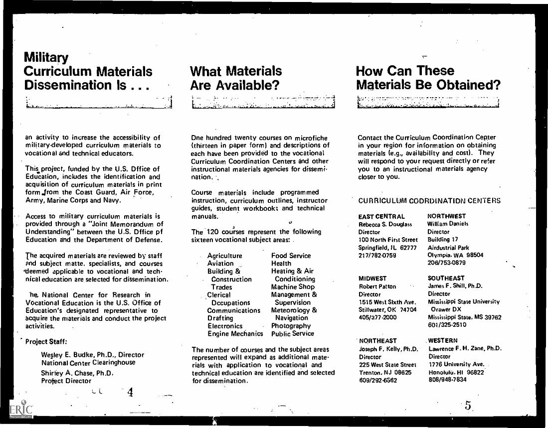
MilitaryCurriculum Materials What MaterialsDissemination Is . . . Are Available?"Lau..L....--..---...loo.:.....i...ja.....j L.I.:-.*.:*'';-,11.-A.P----,,,--;" 'ilt+..;:........1:11iiiiramarial.irarA...1 " TT 7:2
an activity to increase the accessibility ofmilitary-developed curriculum materials tovocational and technical educators.
This.project, funded by the U.S. Office ofEducation, includes the identification andacquisition of curriculum materials in printform jrom the Coast Guard, Air Force,Army, Marine Corps and Navy.
Access to military curriculum materials isprovided through a "Joint Memorandum ofUnderstanding" between the U.S. Office pfEducation and the Department of Defense.
The acquired materials are reviewed by staffand subject matte. specialists, and courses
(deemed applicable to vocational and technical education are selected for dissemination.
'he. National Center for Research inVocational Education is the U.S. Office ofEducation's designated representative toacquire the materials and conduct the projectactivities.
Project Staff:
Wesley E. Budke, Ph.D., DirectorNational Center Clearinghouse
Shirley A. Chase, Ph.D.Protect Director
4
One hundred twenty courses on microfiche(thirteen in paper form) and descriptions ofeach have been provided to the vocationalCurriculum Coordination Centers and otherinstructional materials agencies for dissemination...,
Course materials include programmedinstruction, curriculum outlines, instructorguides, student workbook; and technicalmanuals.
o
The 120 courses represent the followingsixteen vocational subject areas:
AgricultureAviationBuilding &
ConstructionTrades
ClericalOccupations
CommunicationsDraftingElectronicsEngine Mechanics
Food ServiceHea IthHeating & AirConditioning
Machine ShopManagement &
SupervisionMeteorology &
NavigationPhotographyPublic Service
The number of courses and the subject areasrepresented will expand as additional materials with application to vocational andtechnical education are identified and selectedfor dissemination.
1
How Can TheseMaterials Be Obtained?
L.L.::...L.........1
Contact the Curriculum Coordination Cepterin your region for information on obtainingmaterials (e.g., availability and cost). Theywill respond to your request directly or referyou to an instructional materials agencycloser to you.
CURRICULUM COORDINATION CENTERS
EAST CENTRALRebecca S. DouglassDirector100 North First StreetSpringfield, I L 62777217/782-0759
MIDWESTRobert PattonDirector1515 West Sixth Ave.Stillwater, OK 74704405/377-2000
NORTHEASTJoseph F, Kelly, Ph.D.Director225 West State StreetTrenton, NJ 08625609/292.6562
NORTHWESTWilliam DanielsDirectorBuilding 17Airdustrial ParkOlympia, WA 98504206/753-0879
SOUTHEASTJames F. Shill, PhD.DirectorMississippi State UniversityDrawer OX
Mississippi State, MS 39762601/325-2510
. WESTERNLawrence F. H. Zane, Ph.D.Director1776 University Ave.,,Honolulu, HI 96822808/948.7834
%

6
The Nations' Center .,,....,o. re,
Mission.Statement ==
'VI 1 .. ge.r, =#
1 M r'i
smThe National Center for Research in Ei 'AVocational Education's mission is to increase St
2 i 2.the ability of diverse agencies, institutions, ;,,-. r-
3and organizations to solve educational prob. E t=1
et f I glems relating to individual career planning, IT 3-preparation, and progression. The National . -4Center fulfills its missioryby: ii 2
)
Generating knowledge through research
Developing educational programs andproducts
Evaluating individual program,needsand outcomes
Installing educational programs andproducts
Operating information systems andservices
Conducting leadership development andtraining programs
FOR FURTHER INFORMATION ABOUTMilitary Curriculum Materials
WRITE OR CALLProgram Information OfficeThe National Center for Research in Vocational
EducationThe Ohio State University1960 Kenny Road, Columbus, Ohio 43210
6 Telephone: 614/486-3655 or Toll Free 800/848.4815 within the continental U.S.(except Ohio)
6
, Military CurriculumMaterials for
Vocational andTechnical Education
loronn.ilicti ;Ind Field^!vit-xs
Cenint int firs:II:arch;n r_fl
. .
II
V
.
PREPARED FOR
BASIL ELECTRICITY AND ELECTRONICS
CANTRAC A-100-0010
..
MODULE TWENTY FIVE
SPECIAL DEVICES
PREPARED BY
40'INDIVIDUALIZED LEARNING DEVELOPMENT GROUP
SERVICE SCHOOL COMMAND, NTC, SAN DIEGO, CA. 92133
0
STUDY BOOKLET
1 APRIL 1977
1
.
.
14
v
C

Overview Twenty Five
OVERVIEWBASIC ELECTRICITY AND ELECTRONICS
MODULE TWENTY FIVE
Special Devices
In most electronic systemsethere is a need for some sort of controllingor switching action. It may be necessary to modify the incoming signalso that it may be processed for the desired output. An example would '-
be FM Multiplexing in a radio.. In earlier electronics the-controlling/switching action was performed by mechanical relays and rheostats. In
today's high speed computers, however; a mechanlical relay is often tooslow to meet equipment requirements, and rheostats consume too muchpower. Therefore, instead of relays and rheostats, special, devices areused. They are actually "electronic relays/rheostats" or categorically,"electronic switches".
In this module you will study two types:(SCR's) and Unijunction Transistors (U.11"
Yo'il will see as you study the two devicesclassed as controlling or switch devices,operating characteristics.
Silicon. Controlled Rectifierss).
that, though they are boththey have distinctly different
This module has been divided into two lessons:
Lesson I
Lesson II
N
Silicon Controlled Rectifier TheoryUnijunction Transistor Theory
2
9 (

,
1#
O
S
b_.
.
BASIC ELECTRICITY AND ELECTRONICS
ts
MODULE TWENTY FIVE
LESSON 1
SILICON CONTROL RECTIFIER THEORY
.
I APRIL 1977
3 e.'0
es
I
. ".

a
Overview
OVERVIEWLESSON 1it 1,
Silicon Control Rettifier Theory
Twenty Five-1
In this lesson, you will study and learn about Silicon ControlledRectifiers (SCR) You will be able to identify them schematically,as well as, learnthe conditions necessary to start and stop theirconduction. In addition, you will be able to identify physically,schematically and functionally SCR circuits.
The learning objectives of this lesson are as follows:
TERMINAL OBJECTIVE(S):
25.1.47 When the student completes this course, he will be able toTROUBLESHOOT faulty UJT /SCR circuits, given a training de-vide, prefaulted UJT /SCR circuit cards, and proper tools.Repair to be done on a practice board with similar compo-nents.' Repaired board to pass Learning Supervisor's- visualandphysical inspection for quality. Replaced compolient
tested for damage incurred during installation.
ENABLING OBJECTI.VE(S):
When the student completes this lesson, he will be able to:
25.1.47.1 IDENTIFY by selecting, the names of the three leads of anSCR, given an unlabelled diagram of an SCR 'and a list ofnames. 100% accuracy is required.
25.1.47.2 IDENTIFY the conditions necessary to make an SCR startconducting by selecting the correct statement from achoice of four. 100% accuracy is required:
IDENTIFY. the conditions necessary to maintain an SCR inconduction by selecting the correct answer from a choice.of four. 100% accuracy Ls required,
IDENTIFY the conditions necessary to stop conduction of anSCR by,selecting.the correct answer from a cholce of four.1.00% accuracy is required.
25.1.47.3
I25.1.47.4
la
.0

OvervigI
OVERVIEW
Twenty Five-1
25.1.47.5 ,OBSERVE and RECORD waveforms from an SCR AC control circuit,given a training device or circuit and the proper tools,an oscilloscope, a job program, and schematic diagrams ortechnical manuals. Recorded data must be withinlimits shownin the job program.
25.1.47.6 OBSERVE and RECORD waveforms from an SCR DC control circuitgiven a training device or circuit and the proper tools, anoscilloscope, a job program, and schematic diagram or tech-nical manuals. Recorded data must be within limits shown onthe job program.
7,
IEFORE YOU START THIS LESSON, READ THE LESSON LEARNING OBJECTIVES ANDPREVIEW THE LIST OF STUDY RESOURCES ON THE NEXT PAGE.' 4
5

Study Resources Twenty Five -1
LIST OF STUDY RESOURCESLESSON 1
Silicon Control Rectifier Theory
To learn the material in this lesson, you have the option of choosing,according to your experience and preferences, any or all of the followingstudy resources:
Written Lesson presentation in:
Module Booklet:
SummaryProgrammed InstructionNarrative
Student's Guide:
Job Program Twenty Five-1-1 "Silicon Controlled Rectifier DC Control"Job Program Twenty Five-1-2 "Silicon Controlled Rectifier AC Control"Progress Check
Additional Material(s):
Audio/Visual Program Twenty Five-1 "Introduction to Silicon ControlledRettifiers"
Enrichment Material(s):
Basic Electronics Vol. 1, NAVPERS 10087 -C
GE SCR Manual
YOU MAY USE ANY OR ALL, RESOURCES LISTED ABOVE, INCLUDING THE LEARNINGSUPERVISOR; HOWEVER, ALL MATERIALS LISTED AREiNOT NECESSARILY REQUIREDTO ACHIEVE LESSON OBJECTIVES. THE PROGRESS CHECK MAY BE TAKEN AT ANYTIME.
6 13 I

Summary Twenty Five-I
SUMMARYLESSON I
Silicon Controlled Rectifier Theory
4.1
The Silicon Xontrolled Rectifier is a solid state device used in motorcontrollers, switching circuits and power supply circuits. Its advantagesinclude the following:
O
It is quiet in operation.Vibation and shock do not affect it.Most important, you can control a large amount of voltage andcurrent with a small controlling voltage.
We can see froni the schematic symbol shown below that the SCR has 3 'eads.
CATHODE
GATE
The anode and cathodepreviously. The gate
Like a diode, the SCRthe cathode, positive
ANODE
Figure i 4
leads are the same as the diode youlead is added to control conduction
must be forward biased to conduct -on the anode.
have studiedof the SCR.
7 negative on
Figure 2
Unlike adiode, the SCR must have a positive signal on the gate lead(usually 4.1 to +1 v) while it is forward biased or it will not conduct.
14
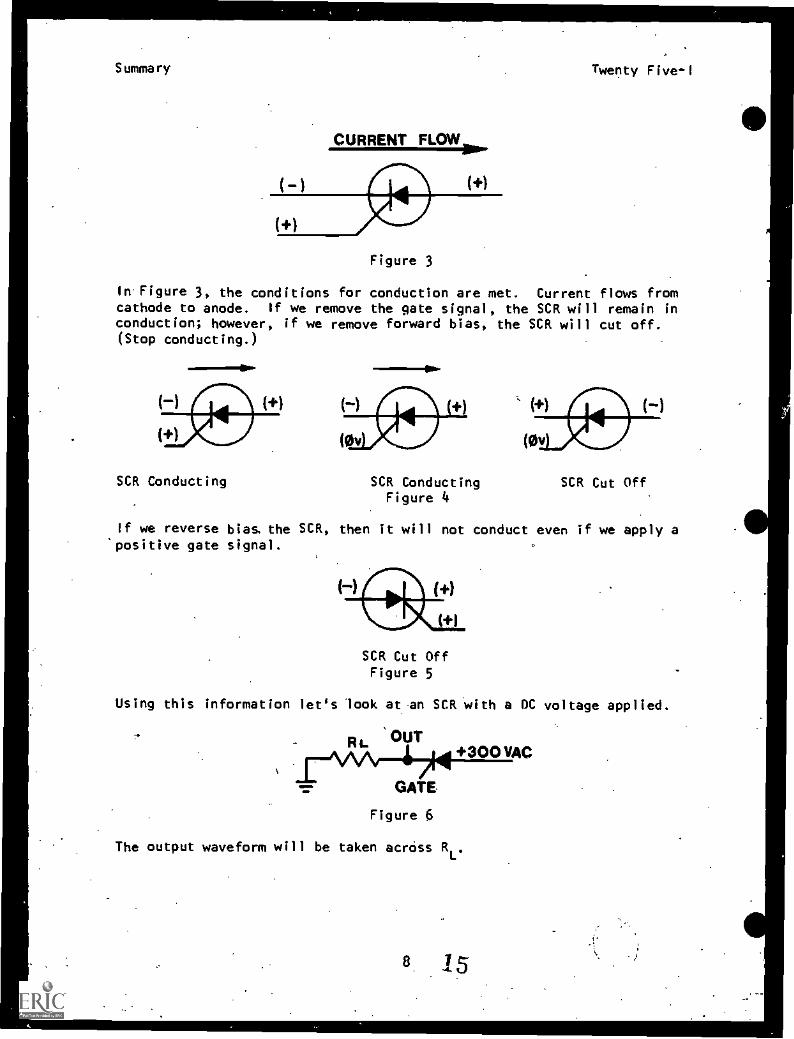
Summary
CURRENT FLOW
(4)
( +)
Figure 3
Twenty Five-1
In Figure 3, the conditions for conduction are met. Current flows fromcathode to anode. If we remove the gate signal, the SCR will remain inconduction; however, if we remove forward bias, the SCR will cut off.(Stop conducting.)11. 111111.
() (+) H (+) ( )
(+) (Ov (ov
SCR Conducting SCR ConductingFigure 4
If we reverse bias. the SCR, then it will not conduct even if we apply apositive gate signal.
SCR Cut Off
( ) I ( +)(+1
SCR Cut OffFigure 5
Using this information let's look at an SCR with a DC voltage applied.
OUT
GATE
Figure 6
The output waveform will be taken across RL.
+300 VAC
Summary Twenty Five -!
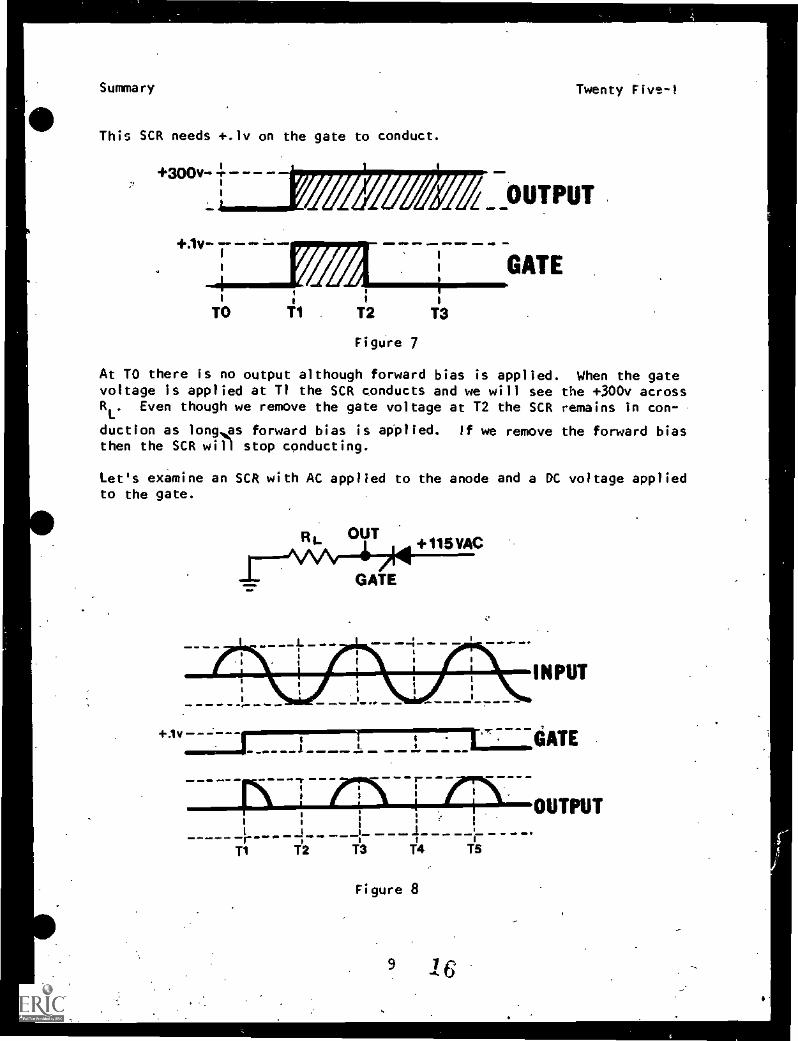
This SCR needs +.1v on the gate to conduct.
Figure 7
At TO there is no output although forward bias is applied. When the gatevoltage is applied at Ti the SCR conducts and we will see the +300v acrossRL
. Even though we remove the gate voltage at T2 the SCR remains in con-
duction as long,,ps forward bias is applied. If we remove the forward biasthen the SCR will stop conducting.
Let's examine an SCR with AC applied to the anode and a DC voltage appliedto the gate.
...MP ..../M ..
1t
1 t
+ 115 VAC
1= IM-1, my. M
1 11 1 1
1 j...,
4-.1v.m..1OM
INPUT
=GATE1 i
-- -4-r-IN .
Ii
I
1 jI
1
1
1r - p I
Ti T2 T2 T4 TS
Figure 8
OUTPUT
Summary Twenty Five-I
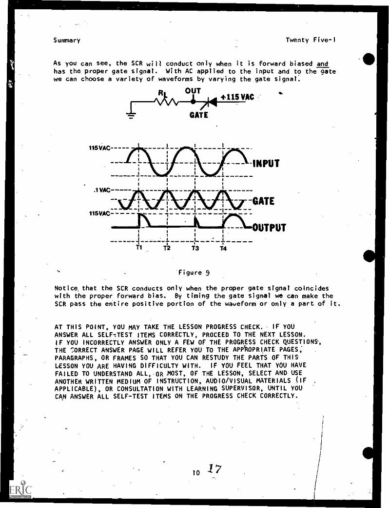
As you can see, the SCR will conduct only when it is forward biased andhas the proper gate signal. With AC applied to the input and to the gatewe can choose a variety of waveforms by varying the gate signal.
OUT+115 VAC
115VAC -
=fp g.a...
.1 VAC -
. --115VAC- -
GATE
=fp a.
1
7 1 -GATE..
1
1
OUTPUT
T1 T2 T3 T4
1
. ........=bra am. 01
INPUT
'Figure 9
Notice that the SCR conducts only when the proper gate signal coincideswith the proper forward bias. By timing the gate signal we can make theSCR pass the entire positive portion of the waveform or only a part of it.
AT THIS POINT, YOU MAY TAKE THE LESSON PROGRESS CHECK.. IF YOUANSWER ALL SELF-JEST ITEMS CORRECTLY, PROCEED TO THE NEXT LESSON.IF YOU INCORRECTLY ANSWER ONLY A FEW OF THE PROGRESS CHECK QUESTIONS-,THE CORRECT ANSWER PAGE WILL REFER YOU TO THE APPrROPRIATE PAGES; .
PARAGRAPHS, OR FRAMES SO THAT YOU CAN RESTUDY THE PARTS OF THISLESSON YOU ARE HAVING DIFFICULTY WITH. IF YOU FEEL THAT YOU HAVEFAILED TO UNDERSTAND ALL, OR MOST, OF THE LESSON, SELECT AND USEANOTHER WRITTEN MEDIUM OF INSTRUCTION, AUDIO/VISUAL MATERIALS (IF .
APPLICABLE), OR CONSULTATION WITH LEARNING SUPERVISOR, UNTIL YOUCAN ANSWER ALL SELF-TEST ITEMS ON THE PROGRESS CHECK CORRECTLY.
101-

P.I. Twenty Five-I
PROGRAMMED INSTRUCTIONLESSON I
Silicon Controlled Rectifier Theory
TEST FRAMES ARE 4, 8, AND 13. AS BEFORE, GO TO TEST FRAME 4 AND SEE IFYOU CAN ANSWER ALL THE QUESTIONS THERE. FOLLOW THE DIRECTIONS GIVENAFTER THE TEST FRAME.
1. The-Sil-iconComIxnJled Rectifier - more commonly called an SCR -is a compact and quiet solid state device. SCR's come in a wide rangeof sizes, operating characteristics and applications.
4
ur.d1.1
Figure 1
110
A 1111....._
of
They can be used in electronic switching circuits, power supply circuitsand motor speed control circuits. When properly chosen and protectedwith cooling fins and heat sinks, the SCR can efficiently control a verylarge amount of power. The SCR, like the diode, is not effected byvibration.
The SCR is very similar to the diode rectifier we covered in previouslessons. A diode, asi-you recall, has an anode and cathode. The SCRhas an anode and cathode with the'addition of a third lead called a"ale. In the SCR schematic, the .gate leadis attached to the cathodeoUthe SCR.
t

P.1. Twenty Five-1'
The schematic symbol for an 5CR is illustrated below. Label the leads ofthe 5CR.
1. Cathode, 2. Anode, 3. Gate
2. Another similarity that exists between the diode and the 5CR is thatthey both must be forward biased in order to Conduct. Also current flowsagainst the arrow in both devices.
Which of the following shows the correct schematic symbol for a forwardbiased SCR?
C.( +)
(-4
c.
1lz

P. I . Twenty Five-I
3. Now that we've looked at the similarities between the diode and theSCR, let's take a look at what makes them operate. The key to under-standing the SCR is in knowing how the gate controls the operation ofthe SCR.
-Figure 2
Unlike the diode, an SCR will not conduct with just forward bias acrossit. The SCR must have a positive voltage applied to the gate at thetime it is forward biased in order for it to conduct. With no voltageon the gate lead the SCR is essentially An open circuit and will notpass any'current.
Figure 3 shows essentially what occurs electronically to a forward biasedSCR with:
(1) no voltage applied to the gate, and(2) a positive voltage applied to the gate.
1. NO CURRENT(OPEN SWITCH)
APPLIED
"SCR OFF"NO CURRENT FLOW
2. MAXIMUM CURRENTFLOW
( +)
GATE
Figure 3
POSITIVE VOLTAGEAPPLIED
"SCR ON"CURRENT FLOW.111111
P.1. Twenty Five-1
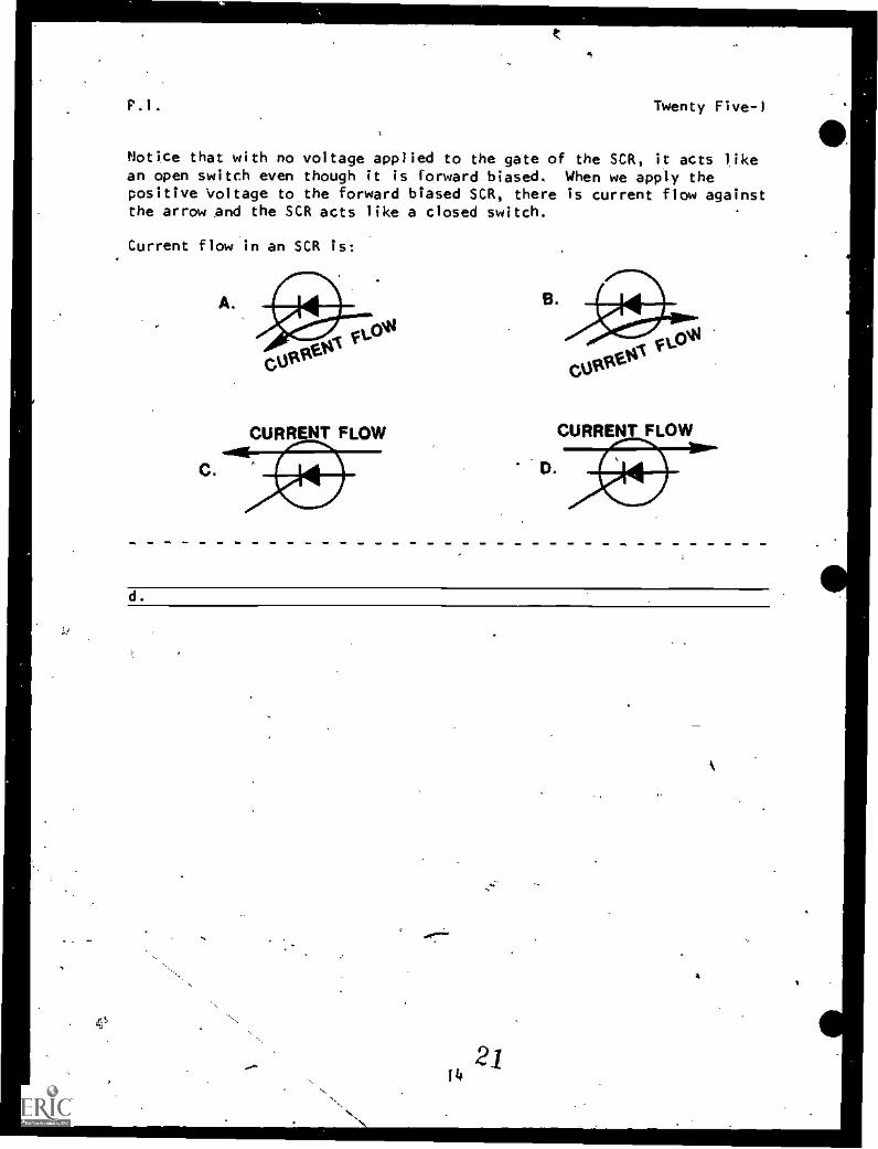
Notice that with no voltage applied to the gate of the SCR, it acts likean open switch even though it is forward biased. When we apply thepositive Voltage to the forward biased SCR, there is current flow againstthe arrow and the SCR acts like a closed switch.
Current flow in an SCR is:
A.
CURRENT FLOW
B.
CURRENT FLOW
D.
d.
2/i

P.1. Twenty Five-1
4. TEST FRAME
a. Label the leads of the SCR in the blanks provided.b. Determine the polarity (with respect to lead 1) of the voltagethat must be applied to each lead to cause the SCR to conduct.c.\ ShoW the direction of current flow.
A. B. C.
(I) ( )
(2) ( )or
(3) ( )
(THIS IS A TEST FRAME, COMPARE YOUR ANSWERS WITH THE CORRECT ANSWERS..GIVEN AT THE TOP OF THE NEXT PAGE.)
15
22
P.I. Twenty Fives-1
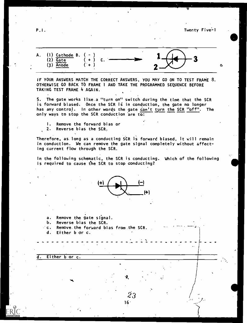
A. (1) Cathode B. ( )
(2) Gate ( + ) C.
(3) Anode ('+ ) 2
IF YOUR ANSWERS MATCH THE CORRECT ANSWERS, YOU MAY GO ON TO TEST FRAME 8.OTHERWISE GO BACK TO FRAME 1 AND TAKE THE PROGRAMMED SEQUENCE BEFORETAKING TEST FRAME 4 AGAIN.
5. The gate works like .a "turn on" switch during the time that the SCRis forward biased. Once the SCR is in conduction, the gate no longerhas any control. In other words the gate can't turn the SCR "off". Theonly ways to stop the SCR conduction are to :'
1. Remove the forward bias or2. Reverse bias the SCR.
Therefore, as. long as a conducting SCR is forward biased, it will remainin conduction. We can remove the gate signal completely without affect-ing current flow through the SCR.
In the following schematic, the SCR is conducting. Which of the followingis required to cause t'he SCR to stop conducting?
a. Remove the gate signal.b. Reverse bias the SCR.c. Remove. the forward bias from the SCR.d. Either b or C.
d. Either b or c.
2316'
- f

P.I.. Twenty Five-1
6. Depending on the circuit application we can apply either a GC levelor an AC signal to the gate of an SCR. In FigUre 4, a DC level of +.4volts is required for the gate to turn the SCR on. Other types of SCRsmay require different voltage levels on the gate to turn them "on".Most of the SCRs you will see will have from +.1 volts to +1 volts appliedto the gate for a turn on voltage.
INPUT
GATEOUTPUT
Figure 4
iovINPUT
1ov.1_ _
o.av
ov- _
TO T1
$
Figure 5
011, qm. =Ma
OUTPUT
Figure 5 illustrates the waveforms of an SCR with DC applied to the gateand with a DC input voltage. Notice that at TO the SCR is forward biasedbut there is no output at TO. Which of the following explains why theSCR is not in conduction?
a. Insufficient forward bias..b. Insufficient DC on the gate.c. The SCR is Reverse Biased.d. Too, much DC on the gate.
r17
24
nd

a.
a
.
P.1. Twenty Five-1
Insufficient DC on the gate...m11mm
I
I
i
I
OV-I
0.8V 10.4V---I
OV 8_
..,M=
10V~ i--1
1
OV-1
I I
TO T1
T
[..
--.INPUT -
Twenty
NPUT ,
----GATE
1
IOUTPUT
I
I I
T2 T3
Figure 6
7. Refer to Figure 6. At time T1 a 6c signal in excess of +.4 volts isappliedeto the gate. The SCR now conducts and we get an output. At timeT2 we remove the DC on the gate. Why does the SCR remain in conduction?
The gate cannot turn off the SCR.
4,
. 25
18
,..,..-",
0
i
P.1.
e
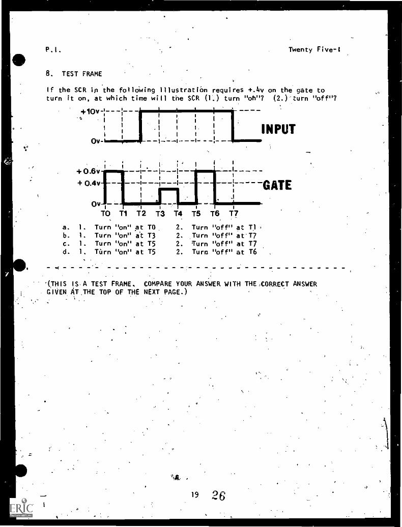
8. TEST FRAME
Twenty Five-1
If the SCR in the follOWing Illustration requires +.4v on the gate toturn it on, at which time will the SCR (1.) turn "oh"? (2.)°turn "off"?
- -
+10V: '1
C. , II
II
Ov-
+ 0.6v
+0.4v
0
11
I II
I 1 I
. 1 I I. I
I I t
--1-:---l- -I- - -- -
I- ;
--1----1---1--I 1 I
I -I- - -1
I
TO T1
a. 1. Turn .0n.
b. 1. Turn "on"c. 1. Turn "on"d. 1. TUrn "on"
_,-I
T2 T3 T4
at TO.it T3at T5at T5
T5
2. Turn2. ,Turn
2. Turn2. Turn
iT6 T7
INPUT
--GATE
"off" at Tl"off" at-T7"off" at T7"off" at T6
.
.(THIS ISA TEST FRAME, COMPARE YOUR ANSWER WITH THEXORRECT ANSWER- GIVEN AT,THE TOP OF THE NEXT PAGE.)
: 1
./0
1
.
4.
19 26,
4

<'
0
.
P.I. Twenty Five -I
c. 1. Turn "on" at T5 2. Turn "off" at T7
IF YOUR AN!+,!-: MATCHES THE CORRECT ANSWER, YOU MAY GO ON TO TEST FRAME 13.OTHERWISE GO BACK TO FRAME 5 AND TAKE THE PROGRAMMED SEQUENCE BEFORETAKING TEST FRAME 8 AGAIN.
9. Now let's'aPply'a DC signal to the gate as an AC signal is appliedacross the anode to cathode of the SCR. The waveforms are illustrated'in Figure 7.
Om. =Mb
0.8V- -1
0.4V--
+10V--- -1-1
1
ov--I
_i
It 1 I
11
1 1 ._iov___ _:._ __ I__ - Ir. ___[___:___ II_ _ _I-
TO T1 T2 T3 T4 T5 Te
mINIEr :MEP .111
-- INPUT
=1.1
-I- - - --GATE1 I "
Illo .1I
:1
Figure 7
- OUTPUTI
.11. Am.
Figure 7 shows that, even. though the SCR,has)been forward biased bythe AC signal from TO to Ti, there is no conduction. This is due tothe fact that there is no positive signal applied to the gate. At Tithe gate voltage is'applied at a sufficient level to cause conduction.
The, SCR still does not conduct because it is reverse biased. T2 arrivesand'we have.the right combination for conduction:
1. A gate signal of sufficJeft level.2. Forward bless from abode to cathode.
2720

P.I. Twenty FiveI
Which of the following statements describes what occurs at T3?
a. The output decreases due to lack of forward bias. .
b. The output decreases due to loss of gate signal.c. The output increases due to the signal on the gate.d. The output increases due to loss of signal on the gate.
a. The output decreases due to lack of forward bias.
0.8V1
0.4V-- 17. _ - :GATE
+10V - - -- _,_-t 1 .
11
OV--- - -1I
1
1
1
-OUTPUTI
1 I
I. I 1 AI1
I.
-10y----;---1---Ir -4- I_ 1_ _i_. 1
TO T1 T2 T3 T4 T5 T6
Figure, B
21 28
MO. .110

P.1. Twenty Five-1
ID. At T4 in Figure 8, the SCR starts conducting and removal of the gatesignal between .T4 and T5 has no effect on its operation. Select thestatement which:
1. Describes the conditions necessary to turn the SCR "on".2. Describes the conditions necessary to turn the SCR "off".
a. (1) Forward bias and sufficient negative signal on the gate.(2) Reverse bias/or remove forward bias.
b. (1) Forward bias and sufficient positive signal on the gate.(2) Remove the gate signal.
c. (1) Forward bias and sufficient negative signal on the gate.(2) Reverse bias/or remove forward bias.
d. (I) Forward bias and a sufficient positive signal on the gate.(2) Reverse bias/or remove forward bias.
d. (1) Forward bias and a suffi'cent positive signal on the gate.(2) Reverse bias/or remove forward bias.
11. So far in our study of SCR's we have used a DC signal on the gate.In these circuits the output waveform has stayed the same'as the inputsignal when the SCR was conducting, and the input signal has been blockedwhen the'SCR was not conducting. Now, we'll see that by using an AC sig-nal as gate and 'also as input signals, control of the SCR becomes smoother.We can pass as little or as much of Ahe positive portion of the AC cycleas we want.
2922
41

P.i. Twenty Five-I
TO Ti Ti2 T3 Tit 7 Tis T7 T8 T? T10 Ili T12, . +10V+ -! I : -I-` - - e- "
II
I 1 1 II/ I
I
1
I1
I iI I I I. I I 8 I
II I I
i I II ..i_ I
M."- '-." 1 I .--11-- -1.-.-- I- INPUTI
, 1 I I 11 1 : I,
1 I 1 I 1 I 11 ,1 1 II I I I I II I I 1 I I I I
/...10V-.8- -- !-- -8--..-8- - -I --.. ..
i-- -1+ 0.4V-1- -8 - -1-- -1---1---1---1- -1
1 I I-1- - -I
I
OV- -:- -1- i-- 1---1-1-I
---1- IGATE-0 .4V -:- -1- --:;- le- 1- i- -1- 771-' 4.- - - I---i
I 1I
I I I - -1--.-.......I...--8..- -1- ..8 - .....1.... --I- -.-I-0.8v- ------+10V- i-- -'I -'4.
I
.. S ... ii. bo . r .s. i am. I . - _ ...,I 1 I i I i
I 1 I1
I i i I II I
1 I
I 1
I
II 1 I
I1 I I
OVI l' I
...-I-I I I I I
I 1 il- IOUTPUT8 I 1 1 1 I I I I I l
I iI I I I 1
II I 1 I I 1
I
I I I I 1 I 1 1 I I I
-10V-II-- ir -1--- ii- -11- --I-- -I- _ g ___ ___I
4. _ _i_ __IL I I I ITO Ti T2 T3 T4 T5 T6 T7 T8 T9 T10 Til T12
Note: The gate waveform is expanded in amplitude with respect to theinput and output waveforms.
Figure 9
Looking at Figure 9, let's assume that the SCR used for these waveformsrequires a +.4 volt signal on the gate to enable the forward biased SCRto conduct. Notice that the SCR still operates in. the same manner butour output waveform is different.
Although the SCR is forward biased at TO, the AC gate signal does not'each +.4v until T2. At this time the gate signal is of sufficientamplitude to cause the forward biased SCR to conduct. Even though thegate voltage immediately drops below .4 volts, the SCR continues to con-duct until the forward bias is removed at Tit. This action is repeatedagain at T10.
233.0 . -
Twenty Five-1
How does the power output of the SCR device in Figure 9 compare with 'thepower output of the same device with a continuous +.4 volt DC signalapplied to the gate?
a. The power is the same iii both cases.b. The power output in Figure 9 is less.c. The power output in Figure 9 is greater.
b.. The power output in Figure 9 isNote:. The device with the +.4 voltpass the entire positive portion ofin Figure 9 passes only about half
less.
DC signal applied to the gate willthe inputcycle whereas the device
of the positive input alternation.
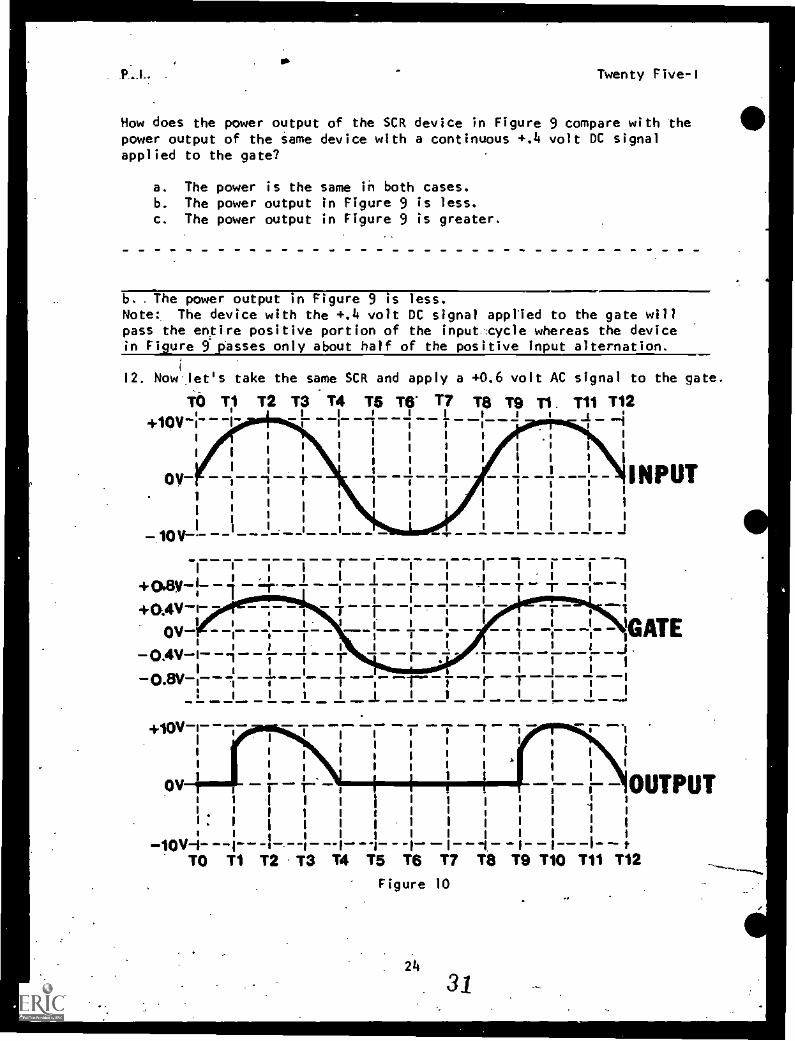
12. Now jet's take the same SCR and apply a +0.6 volt AC signal to
TO T1 T2 T3 T4 T5 Te" 17 Te T9+10V -1--1-
1-1-'I
1 1 1_11 I 11111
11 1 1 1 1
1
1IIII 1
1 1111 8 I 1-I- -4.___ _4_ _4___I... INPUT
1
81111181II I 1 1 1 i I I
.r
Tl. T11 T12
oV-,
1I I
- boy--
the gate.
11 117-1 II III 1 -1+ 4-
8
+0.4V-1- Tr':GATE
I I
I I Iqplo -. MOM 4. .PDOV 1 eI
1 i I-0.4V-1^ --I . 1"
i 1 8.
1 t 1 i-0.8V I1 8 I 1
mllo ,, 11M 4... IND 4. .I 4.
+10V-1 ----
I 8 1I 1_
8 I8 II 1-ov r T-
1 1 1 I I 1 1 8
I I I
1
l I I 1 I I 1
1111611_11r T ,
-t
I II I
I 1 I1 II
I lilt, III-iov-i- --r- -1-- -1- -I-
TO T1 T2 T3 T4 T5 T6 T7 T8 T9 T10 T11 T12Figure 10
OUTPUT
31
P.I. Twenty Five-1
Note: The gate waveform is expanded in amplitude with respect to theinput and output waveforms.
It can be seen that the gate signal now rises to the +.4 volt level attime T1. This allows more of the positive portion of the input cycle tobe passed through the device which, in turn, increases the power output.
If we increased the AC gate signal to an even greater amplitude -- sayone volt for example -- the SCR would conduct almost as soon as it wasforward biased and all of the positive portion of the AC cycle would bepassed. We have developed a method of controlling the exact amount ofpower we allow through the SCR device.
What is the minimum AC gate voltage in Figure 10 that will cause the SCRto conduct?
a. +0.6vb. -0.4vc. +0.4vd. -0.6v
c. +0.4v
13. 'TEST FRAME
How do we vary the amount of positive AC signal passed by a forward biasedSCR?
a. Vary the signal on the cathode.b. Vary the signal on the gate.c. Vary the signal on the anode.d. Vary the forward bias.
(THIS IS A-TEST FRAME. 'COMPARE YOUR ANSWER WITH THE CORRECT ANSWER GIVENAT THE TOP OF"THE NEXT PAGE.)
.._
--
25
.

.,
P. I . Twenty Five-I
b. Vary the signal on the gate.
IF YOUR ANSWER MATCHES THE CORRECT ANSWER YOU HAVE COMPLETED THE PRO-GRAMMED INSTRUCTION FOR LESSON I, MODULE TWENTY FIVE. OTHERWISE GO BACKTO FRAME 9 AND TAKE THE PROGRAMMED SEQUENCE BEFORE TAKING TEST FRAME 13MAIN.
AT THIS POINT, YOU MAY TAKE THE LESSON PROGRESS CHECK. IF YOUANSWER ALL SELF-TEST ITEMS CORRECTLY, PROCEED TO THE NEXT LESSON.IF YOU INCORRECTLY ANSWER ONLY A FEW OF THE PROGRESS CHECK QUESTIONS,THE CORRECT ANSWER PAGE WILL REFER YOU TO THE APPROPRIATE PAGES,PARAGRAPHS, OR FRAMES SO THAT YOU CAN RESTUDY HE PARTS OF THISLESSON YOU ARE HAVING DIFFICULTY WITH. IF YOU FEEL THAT YOU HAVEFAILED TO UNDERSTAND ALL, OR MOST, OF THE LESSON, SELECT AND USEANOTHER WRITTEN MEDIUM OF INSTRUCTION, AUDIO/VISUAL MATERIALS (IFAPPLICABLE), OR CONSULTATION WITH LEARNING SUPERVISOR, UNTIL YOUCAN ANSWER ALL SELF-TEST ITEMS ON THE PROGRESS CHECK CORRECTLY.
332b

Narrative Twenty Five-I
NARRATIVELESSON I
Silicon Controlled Rectifier Theory
the silicon controlled rectifier, commonly called an SCR, is a compactand quiet solid state device. Its operation is unaffected by vibrationand shock. When properly chosen and protected with heat sinks andcooling fins, the SCR can efficiently control a very large amount ofpower.
SCR's come in a wide range of sizes, operating characteristics andcircuit applications. When used properly they should have virtuallyunlimited operating life.
4. Jr
,,4111111k
'.roe,
Figure 1
'27
`%.
34
, 7
au.anNir"
Narrative Twenty Five-I
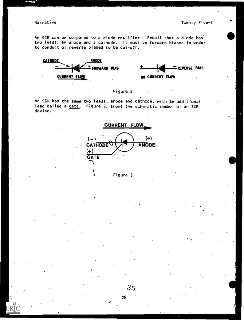
An SCR can be compared to a diode rectifier. Recall that a diode hastwo leads; an anode and a cathode. It must be forward biased in orderto conduct or reverse biased to be cut-off.
CATHODE AN
FORWARD BIAS
CURRENT FLOW
4:---/11111=- REVERSE BIAS
NO CURRENT FLOW
Figure 2
An SCR has the same two leads, anode and cathode, with an additionallead called a gate. Figure 3, shows the schematic symbol of an SCRdevice.
CURRENT FLOW
( -)
CATHODE( +)GATE
1V
Figure 3
(+)
3528
ANODE
- -
Narrative Twenty Five-i
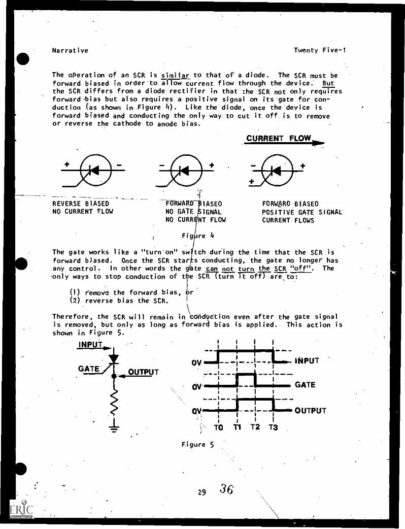
The operation of an SCR is similar to that of a diode. The SCR must beforward biased in order to allow current flow through the device.' But
the SCR differs from a diode rectifier in that the SCR not only requiresforward-bias but also requires a positive signal on its gate for con-duction (as shown in Figure 4). Like the diode, once the device isforward biased and conducting the only way to cut it off is to removeor reverse the cathode to anode bias.
+
REVERSE BIASEDNO CURRENT FLOW
CURRENT FLOW
FORWARD IASED FORWARD BIASEDNO GATE IGNAL POSITIVE GATE SIGNALNO CURR NT FLOW CURRENT FLOWS
Figure 4
The gate works like a "turn on" sw tch during the time that the SCR isforward biased. Once the SCR star s conducting, the gate no longer hasany control. In other words the g to can not turn the SCR "off". Theonly ways to stop conduction of t e SCR-Tturn it ofTrare.to:
(1) eemove the forward bias, r
(2) reverse bias the SCR.
Therefore, the SCR will remain in\coriduetion even after the gate signal
is removed, but only a$ long as forwar4 bias is applied. This action isshown in Figure 5.
INPI.M._ 1 1 I 1---.-- 1 I..... .., ..... ..,,.
/ , INPUTGATE' OUTPUT
coi-1
1-..
AY
,:- : - - - I--CAr GATE
i I I i
OY --1
I-- OUTPUT, 1 1
.1` TO 11 T2 T3
Figure 5
29 36
,
vr
.
0
Narrative Twenty five-I
An SCR requires (forward/reverse) bias and a (positive/negative) gatesignal to enable it to conduct.
forward;_positive
Which of the following is required to cause an SCR to stop conducting:0
a. simultaneous removal of the gate signal and continued forwardbias application.b. removal of the gate signal.c. reverse bias the SCR.d. either b or c
c. reverse bias the SCR (removing the forward bias -is also sufficientto cause the SCR to stop conducting).
3130
to
p -.
0.
Narrative Twenty Five-I
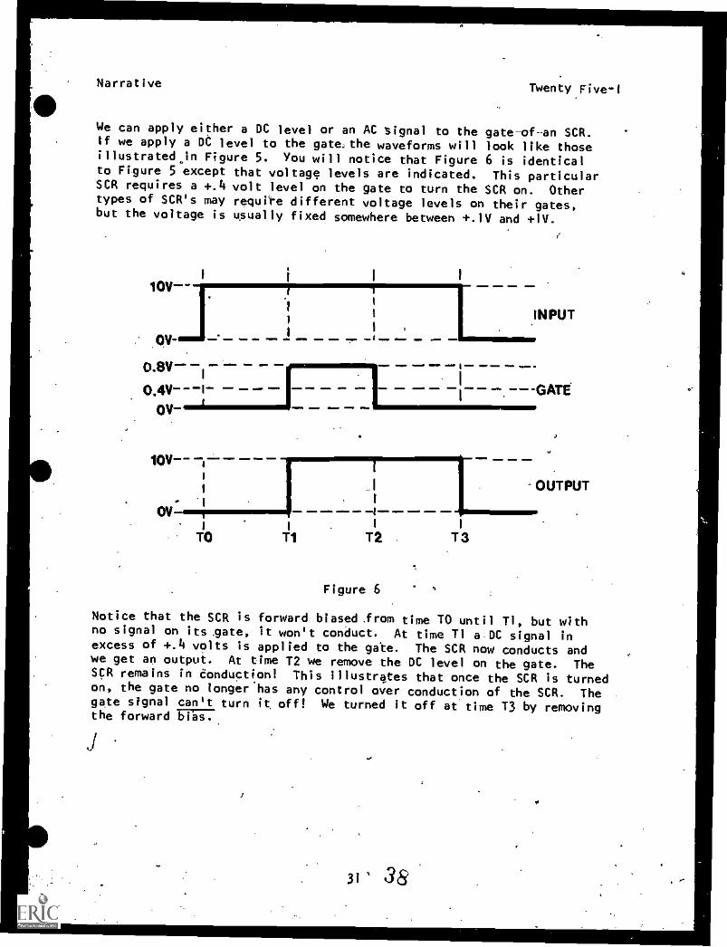
We can apply either a DC level or an AC signal to the gate -of -an SCR.If we apply a DC level to the gate: the waveforms will look like thoseillustrated in Figure 5. You will notice that Figure 6 is identicalto Figure 5 except that voltage levels are indicated. This particularSCR requires a +.4 volt level on the gate to turn the SCR on. Othertypes of SCR's may requrre different voltage levels on their gates,but the voltage is usually fixed somewhere between +.1V and +1V.
..
1
!1
i1
I
. liI INPUTI
0.0.....-1.... _ _ .... WRO . .m. 4, No _GatOV-
10V_- --1
I
i
I
TOi
T1
I
1 -[- OUTPUT. I
11. ..mmq. .
I i
T2 T3
Figure 6 4
Notice that the SCR is forward biased from time TO until T1, but withno signal on its_gate, it won't conduct. At time T1 a DC signal inexcess of +.4 volts is applied to the gate. The SCR now conducts andwe get an output. At time T2 we remove the DC level on the gate. TheSCR remains in donductionl This illustrates that once the SCR is turnedon, the gate no longer has any control over conduction of the SCR. Thegate signal can't turn it, off! We turned it off at time T3 by removingthe forward bra.
1
314 38
4
JO
Narrative Twenty Five-I
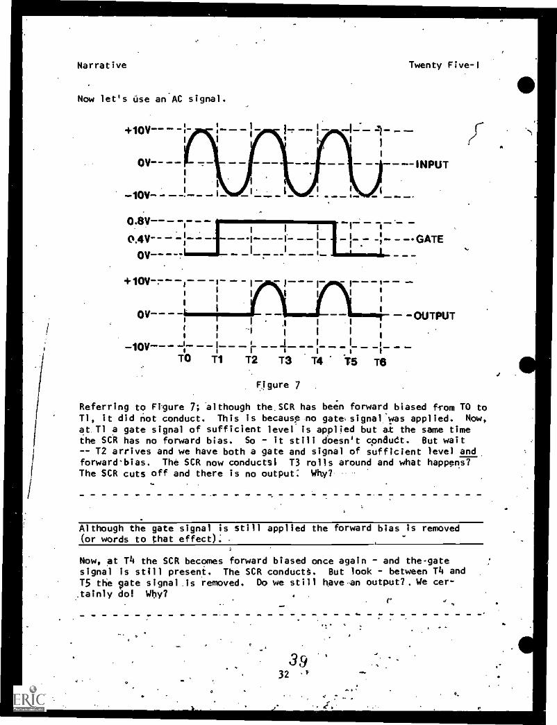
Now let's use an AC signal.
0.8V --1
0.4V-- 1--- --1-- -- r --- 1 1 . 1 --GATEOV
i
_1_ I 1_-- ,I
+10V s
I.
TO T1 T2 T3 T4 TS TO
figure
0 V
. .11M gms.
mla
OUTPUT
Referring to Figure 7; although the SCR has been forward biased from TO toTl, it did not conduct. This is because no gatesignal.was applied. Now,
at Tl a gate signal of sufficient level is applied but at the same timethe SCR has no forward bias. So - it still doesn't candudt. But wait-- T2 arrives and we have both a gate and signal of sufficient level andforward bias. The SCR now conducts! T3 rolls around and what happens?The SCR cuts off and there is no output: Why?
Although the gate signal is still applied the forward bias is removed(or words to that effect);
Now, at T4 the SCR becomes forward biased once again - and the-gatesignal is still present. The SCR conducts. But look - between T4 andT5 the 'ate signalis removed. Do we still have-an output?. We cer-.tainly do! Why? .
. rMgr "39
32
s' 7
r, .
mew
0,

0
Narrative Twenty Five -1
Once the SCR starts conducting removal of the gate signal is notsufficient cause tb cut it off. Only removal of forward bias - orapplication of reverse bias - can turn it off. (or words to..that
effect.)
Now, that wasn't so difficult, was it? So far we've seen a DC levet aiboth the gate signal and the input signal: and we've just looked at asituation where the gate signal was DC and the input was AC.Aat's nowsee-what happens when we use AC as both gate and input signal. For thisexample let's also assume we're using an SCR which requires a minimum+.4 volts on the gate to enable the SCR to conduct. '(Remember - it mustalso be fdrward biased.)
TO Ti T12 Til If T5 TIV Ti T8 T9 T 0 T11 T12+101,; --I 1 I 1
A . 1
1 11 1
i
. 1 1
1 1
1. A ; 11
1
1 1
1
I1
1
1
1 r 1. 1 I1 1 - 1 ! 1
III.
1 _ ;l_.__:_ ..1.......1_1 r i 1
1 11 I I
1 .I I I ;/ -* 1 ' r i I
1 11 ; .1
I1
I. i,
I
1 I r* 1
_iov__L __!__*_:__ _1___i___ 4.1w 1.1 .I .N1 L /0.8V --I-- 1-- i--- I --1---I I
W' O
IMNP-1 ..
i I I I A101. W.D. l 1, I I' ,
CI 41,--1"--8 1 1-j
1 1 ' 1
0V-' $I 1 1 1
-' r--r-- -1---1---1-- --11---1- rI
GATE__I__ 10.4V-1 -- i . i---. I 1--- I .1 i
I / I IoilyL._ ._ __I _ _J.. _ .1__ __g --. _ I _ _.!,___s_ __ ..1
+10V t---i--- _--,,_,,___,___,___....__,__ ----1t 1
11 1
1
I. 1 1 I 1 I 1
I 11 1 I 1
1 1
CAI -1- - ,1 I ' I 1
NPUT
1 .1 I I I I. i1
1 1 1 1 I 1 1 I 1
I
-1011-1----1---;:7-1---1---j-----7e rH-;---1---,TO T1 T2 T3 T4 T5 T8 T7
1
T8 T9 TIO T11 T12
1
OUTPUT1
I I
Figure 8
Looking Fifure 8 we see an output signal of yet another wave shape.The same basic SCR concept applies. It must be forward biased and thegate signal' must be of sufficient level to enable the SCR to conduct, -In this'case, as the.gate signal peaks at 12 and again at TlO it is ofa sufficient level, +.4 volt,to cause the forward biased SCR to conduct.
33. 40

-
Narrative Twency Five:1
Now let's take the same SCR and apply an AC gate signal with a peakamplitude of +.6 volts. First we will expand our time chart andexamine what is happening en the gate.
TO T1 T2 T3 T4 T5 T6 Ti T8 T9 T10+0.8v -1 I 1 1 1 1 I
II t 1 .. s
i $ SCR CONDUCTION LEVEL TIME FOR "B" I -'1
--7*---T---1---77--r -1-- -1-8--I I i s I I
I 0
I I I I . 1 t+.0.4147-.i 8j a
1
,I.
I
I I
I 11 Or ....).Oje 1
+0.2v-ir- A-- - 1% -1 I i 1 I ,
--i- -r .- -7.71 4, 1
1 14 1s i I 1 s
I
OV .. _,r . _i 1
__. __!..... 1_ _ _i_1
---!-P-- 1- GATE1 I
4I
II
01 1 , . I
It.it 1 WAVEFORM
1 1 ILI . 1 1- 0.2v-r- --I- -- - -t - -i- - 1 - - - r-I I s 1 I N% I I 1
Ii
I I a 1 1 1 , 1 1- 0.4v-I-- -1 -7- T 1 -30..tror- - - r'--T--;I 1 1 I I 1 I 1 I I1 I I * I I 1 I I''' 0.811T " -
i I I II
I i i SCR CONDUCTION LEVEL TIME FOR "A"-7._ri -._.1.__ 10.
TO T1 T2. 14 14 TS To 7 8 T9 T.
Figure 9
Look at waveform "A" first. It is the same waveform we applied to the'gate of the SCR in Figure 8., It's of low amplitude peakingiat +.4 volts,the level sufficient to cause the forward biasred SCR to-conduct. It
reaches this level at T2.' Now, look at waveform "B",,our.new input sig-nal on the gate. it's of a much greater amplitude. It also peaks at T2- but - it reaches +.4 volts at 11, much earlier than did,waveform "A".Thirefore, the forward biased SCR is able td conduct much earlier,allowing more of 'the input to pass through the device tothe.output asshown in Figure 10.
34
a

.
Narrative Twenty Five-1
TO T1 T2 T3 T4 15 T6 17 Te T9 T1 T11 132s$ 11 1 1 i 1 1+10Vr 1 II I 1 1
1 1
I I I 11 I 1 I I
a I1
II 1
I1
I
INPUT1 I1 --TV 1 i'1
I I I I 1 1 1
I I I 1 1 1 II 1 1 I II i p
1 i 1 i i1 11-- 1 T i I I 1 1 1 I1 1 1 1 1 f 1 s 1
+.8V '1 -7` 1 I 1 r T 1 i1 I I I I
+.4V-1 _ _1 ; 1
ri
_ _1
ov__ _...,.__..,-- _ I -r s T 1 1
1 GATE1 1-.4V-i- -I r --; r1 .... Ir 1 I 1 1 jII es1111 Is .1 --11
-1i_o_. I-1_ i_ i
,I I I I I
1 1 1 , 1 1 1 I I .1 ,
1 1.2 .L.--1 , . i I 1 1oov-i---,- r ,-,
1 11
1 11
1, 1 1 1
I I1
I1 1 I I I 1
,ri r 1 I ;-- OUTPUT=...1 I 1
I 1 1 I 1 1 I 1 1 I II iii 1 1 1 I I i 1 I ; 1 0IIIIIIIIIII: 1IIIIIIIIIII10V-1 1 I -1 --I 1 r- 1-- I I 1- - -1-- t
TO T1 T2 T3 T4 TS Te 17 Te T9 T10 T11 T12Figure 10
This increase in output power can readily be seen by comparing theoutput waveform in Figure 10 to the output waveform in Figure 8.
Silicon Controlled Rectifiers have many applications. Depending on
your rating you will see certain of these applications. They are
used in motor speed control circuits, electronic switching circuitsand power supply rectifiers, among others.
I s 1
. Oil- -I- -1 TI 1 ' I
.1 1 1
I 1 1
I AI _i_ 1 _, ___
10V7r 1 j 1 o 1i 1 1 I 1 t
42_35
A
Narrative Twenty Five-I
AT THIS POINT, YOU MAY TAKE THE LESSON PROGRESS CHECK. IF YOU
ANSWER ALL SELF-TEST ITEMS CORRECTLY, PROCEED TO THE NEXT LESSON.IF YOU INCORRECTLY ANSWER ONLY A FEW OF THE PROGRESS CHECK QUESTIONS,THE CORRECT ANSWER PAGE WILL REFER YOU TO THE APPROPRIATE PAGES,PARAGRAPHS, OR FRAMES SO THAT YOU CAN RESTUDY THE PARTS OF THISLESSON YOU ARE HAVING DIFFICULTY WITH. IF YOU FEEL THAT YOU HAVEFAILED TO UNDERSTAND ALL, OR MOST, OF THE LESSON, SELECT AND USEANOTHER WRITTEN MEDIUM OF INSTRUCTION, AUDIO/VISUAL MATERIALS (IFAPPLICABLE), OR CONSULTATION WITH LEARNING SUPERVISOR, UNTIL YOUCAN ANSWER ALL SELF-TEST ITEMS ON THE PROGRESS CHECK CORRECTLY.
.
36

BASIC ELECTRICITY AND ELECTRONICS
MODULE TWENTY FIVE
LESSON 11
UN1JUNCTION TRANSISTOR THEORY
1APRIL 1977
9/
14
Overview. Twenty Five-II
OVERVIEWLESSON II
Unijunction Transistor Theory
In this lesson, you will study and learn about Unijunction Transistors
(UJT). You will be able to identif7 them physically and scheMatically.You will also be able to identify the necessary voltage, current and
'resistance relationships present in a Unijunction Transistor.
%
The learning objectives of this lesson are as follows:
TERMINAL OBJECTIVE(S):
25.2.47 When the student completes this course, he will be able toTROUBLESHOOT faulty UJT/SCR circuits, given a training de-vice, prefaulted UJT/SCR circuit cards, and proper tools.Repair to be done on a practice board with similar compo-nents. Repaired board to pass Learning Supervisor!s visualand physical inspection for quality. Replaced compohent..to
be tested for damage incurred during installation.
ENABLING OBJECTIVE(S):
When the student completes this lesson, he will be able to
25.2.47.7 IOENT1FY by matching, the names of the three leads of a UJTgiven an unlabelled diagram of a UJT and a list of names.100% accuracy is required.
25.2.47.8 IDENTIFY the conditions necessary to make a UJT conductby selecting the correct statemen of conditions from achoice of.four. 100% accuracy is required.
25.2.47.9 DEFINE the term "voltage gradient" as Lt applies to a UJTby selecting the correct answer from a choice of four.100% accuracy is required.
25.2.47.10 IDENTIFY the conditions necessary to maintain conduction ofa UJT by selecting the correct answer from a choice of four.100% accuracy is required.
25.2.47.11 IDENTIFY the conditions necessary to stop conduction of aUJT by selecting the correct answer from a choice of four.100% accuracy.is required.
t.;%.
38

-A,
Overview Twenty Five-II
OVERVIEWV
25.2.47.12 OBSERVE and RECORD normal waveforms from a UJT sawtooth gen-erator circuit given a training device, a job program, proper
. tools, an oscilloscope, a signal generator, and applicableschematic diagrams or technical manuals. Recorded data mustbe within limits stated in job program.
25.2.47.13 OBSERVE and RECORD waveforms from a UJT multivibrator circuitgiven a training device, proper tools, an oscilloscope, asignal generator, a job program, and schematic diagrams ortechnical manuals. Recorded data must be within limits statedon the job program.
25.2.47.14 OBSERVE and RECORD normal waveforms from a UJT trigger circuitgiven an applicable training device or circuit and the propertools, an oscilloscope, a signal generator, a job program, andschematic diagrams or technical manuals. 100% accuracy is re-quired.
25.2.47.15 LOCATE a faulty component in a SCR control circuit/UJT rampgenerator circuit by discriminating between normal andabnormal waveforms froma prefaulted training device or cir-cuit, and using the proper tools, an oscilloscope, a signalgenerator and given a job program and schematics or technicalmanuals. 100% accuracy is required.
BEFORE YOU START THIS LESSON, READ THE LESSON LEARNING OBJECTIVES ANDPREVIEW THE LIST OF STUDY RESOURCES ON THE NEXT PAGE. .
39
Study Resources Twenty Five-II
LIST OF STUDY RESOURCESLESSON II
Unijunction Transistor Theory
To learn the material in this lesson, you have the option of choosing,according to your experience and preferences, any or all of the follow-ing study resources:
t;
Written Lesson presentation in
Module Booklet
SummaryProgrammed InstructionNarrative
Student's Guide:
Job Program Twenty Five-11-1 "Unijunction Transistor Sawtooth/TriggerGenerator"
Job Program Twenty Five-11-2 "UoIjunction Transistor Multivibrator"Job Program Twenty Five 11-3 "UJT Ramp Generator and SCR Control
Circuit"Progresi Check
Additional Material(s):
Audio/Visual Program Twenty Five-II "Introduction toUJT's"
Enrichment Material(s):
Basic Electronics, Vol. 1, NAVPERS 10087-C
YOU MAY USE ANY, OR ALL, RESOURCES LISTED ABOVE, INCLUDING THE LEARNINGSUPERVISOR; HOWEVER, ALL MATERIALS LISTED ARE NOT.NECESSARILY REQUIREDTO ACHIEVE LESSON OBJECTIVES. THE PROGRESS CHECK MAY BE. TAKEN AT ANYTIME

Summary
0
SUMMARYLESSON .11
Unijunction. Transistor Theory
Twenty Five-11
The Unijunction Transistor is a solid state device used in switching andtiming circuits. Its physical appearance Is identical to a common tran-sistor. .
UJT TRANSISTOR
A second base lead instead of a collector is the major difference betweena UJT and a'transistor. The schematic symbol for a UJT looks like this:
The lead with the arrow is the emitter; Base 1 (B1) is' the lead,to whichthe emitter arrow points; the Base ,2 (B2) is the other lead. Base 2 canbe compared to the collector of a common transistor in that Base 2 isusually where Vcc is applied.
Proper operation of a UJT depends upon proper bias. The UJT must havea positive voltage level on Base 2 and a less positive voltage level onBase 1.
al 48
Summary Twenty Five-11
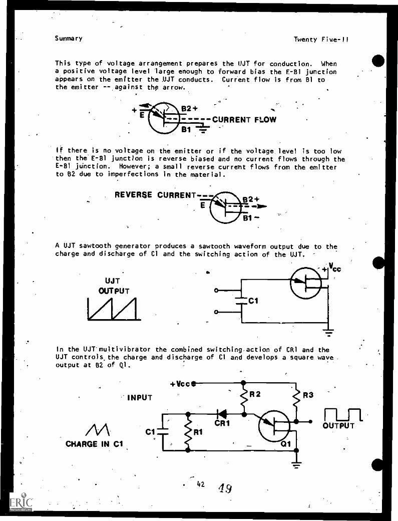
This type of voltage arrangement prepares the UJT for conduction. Whena positive voltage level large enough to forward bias the E-81 junctionappears on the emitter the .UJT conducts. Curr'ent flow is from 81 tothe emitter --,against thf arrow.
82+--CURRENT FLOW
If there is no voltage on the emitter or if the voltage level is too lowthen the E-81 junction is reverse biased and no current flows through theE-81 junction. However; a small reverse current flows from the emitterto 82 due to imperfections in the material.
REVERSE CURRENT.-- 82+
81
A UJT sawtooth generator produces a sawtooth waveform output due to thecharge and discharge of CI and the switching action of the UJT.
UJTOUTPUT
In the UJT'multivibrator the combined switching.action of CR1 and theUJT controls the charge and discharge of Cl and develops a square waveoutput at 82 of Ql.
INPUT
CHARGE IN
. 424.9
OUTPUT

i
Summary
\Twenty Five- I I \
A trigger circuit may be constructed by removing CR1 and RI from themultivibrator circuit and placing a resistor between Bl and ground.The output is taken from Bi of the UJT. The schematic diagram of atypical UJT trigger circuit is:
I'Veg
C1 WAVEFORM
..,
Cr
AT THIS POINT, YOU MAY TAKE THE LESSON PROGRESS CHECK. I.F YOU
ANSWER ALL SELF-TEST ITEMS, CORRECTLY, PROCEED TO THE NEXT LESSON.IF YOU INCORRECTLY ANSWER ONLY A FEW OF THE PROGRESS CHECK QUESTIONS,THE CORRECT ANSWER PAGE WILL REFER YOU TO THE APPROPRIATE PAGES,PARAGRAPHS, OR FRAMES SO THAT YOU CAN RESTUDY THE PARTS OF THISLESSON YOU ARE HAVING DIFFICULTY WITH. IF YOU FEEL THAT YOU HAVE,FAILED TO UNDERSTAND ALL, OR MOST, OF THE LESSON, SELECT AND USEANOTHER WRITTEN MEDIUM OF INSTRUCTION, AUDIO/VISUAL MATERIALS (IFAPPLICABLE), OR CONSULTATION WITH LEARNING SUPERVISOR, UNTIL YOUCAN ANSWER ALL SELF-TEST ITEMS ON THE PROGRESS CHECK CORRECTLY. .
.
.
P.1. Twenty Five-11
PROGRAMMED INSTRUCTIONLESSON II
- Unijunction Transistor Theory
TEST FRAMES ARE 6 AND 13. AS BEFORE, GO TO TEST FRAME 6 ANO SEE IF YOUCAN ANSWER ALL THE QUESTIONS THERE. FOLLOW THE DIRECTIONS GIVEN AFTERTHE TEST FRAME:
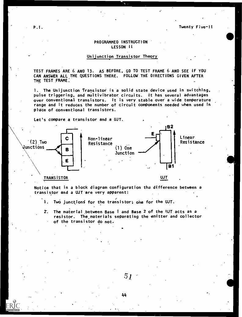
1.. The Unijunction Transistor is a solid state device used in switching,pulse triggering, and multivibrator circuits. It has several advantagesover conventional transistors. It is very stable over a wide temperaturerange and it reduces the number of circuit components needed when used inplace of conventional transistors.
Let's compare a transistor and a UJT.
Non-linear(2) Two Resistance
unctions (1) One\ Junction
. \
82
TRANSISTOR UJT
LinearResistance
1
Notice that in a block diagram configuration tha difference between atransistor and a UJT are very apparent: .
4
. ,1. Two junctions for the transistor; one for the UJT.
2'. The material between Base i and Base 2 of the 11.1T acts as aresistor. The materials separating the emitter and collectorof the transistor do not.
. .
44

P.I. Twenty Five-II
In physical appearance however, the transistor and the UJT are identical.
I I 1
TRANSISTOR,
B1
UJT
B2
You can see that the tab on the case of both devices denotes the emitter.The lead configuration is the same. If we move in a clockwise directionfrom the emitter on ,the UJT, the first lead we encounter is Base 1; thesecond lead is Base 2. This is another difference between a transistorand a UJT.
Now, let's look at the schematic symbol of a UJT as compared to that ofa transistor.
TRANSISTOR UJT
Quite a bi: of difference here, isn't there?
You have a'ready learned which lead is which in the transistor symbol soit will be easy to identify the UJT leads. The lead with the arrow isthe emitter. The lead to which the arrow points is Base 1. That leavesone other 'ead Base 2.
142

n
P.I.0
at*-
Twenty Five-II
.
.- .
Label the leads of the UJT in each of the below Ilustrations:. .
.
A. 1: Emitter 2. Base 1. 3. Base 2B. 1. Emitter 2. Base 1 3. Base 2'
I. Alltypes of transistors or diodes need a certain.bias level to oper-ate. The UJT is no different. Base 2 of a UJT mustbe connected to somepositive value. Base 1 must be at ground potential or some valueof voltage less than that on Base.2).
.
Is the UJT in the illustration below properly biased for correct operation?
yes
1' c.
AP

1
P.1. Twenty Five -il
3. Let's connect a known voltage to theALIT.
10VDC
.If we connect a voltmeter between the Base I and Base 2 leads we will readthe full.ten volts.
10v
However, if we could take a reading at some point between the two baseleads we would read a value less than ten volts.
a
a
The'area between theliase leads is acting like a resistor. At differentPoints we read different voltage levels. This sequential rise in potentialis called a Voltage Gradient.
<1
O
The material between Base 1 and Base 2 of a UJI acts like a/anand the differ4hoe in potential is called a/an
o. .147 "54
.4:

P.1. Twenty Five-11
resistor, voltage gradient lin that order)
4. The emitter of.the UJT acts like the wiper arm of a variable resistor.Althuugh it does not physically move, it does feel the potential of thevoltage gradient opposite it.
in this case the emitter feels a positive 4 volts. The voltage levelthe emitter feels is the conduction point voltage needed to turn on theUJT. This turn on voltage is determined by the type of UJT and isestablished at the time of construction.
What is the conduction point of the UJT illustrated below?
7 volts (6 1/2 - 7 1/2 acceptable)
5. You have seen how the bias voltage is developed between Base 1 and
Base 2. How let's see what happens when we apply a voltage to the emitter.
55
48

P.I. Twenty Five-II
If we apply a voltage level to the emitter that is greater than the differ-ence of potential opposite the emitter-Base I junction, then the LIXT willconduct heavily through the emitter-Base 1 junction.
If the voltage level on the emitter drops below the level of the potentialdifference opposite the emitter, then the emitter-Base 1 junction actslike an open circuit and no current flows.
1
REVERSE CURRENTs 10V
NO CURRENT
However, a small current will flow between the emitter-Base 2 junction.This small amount of current is called reverse current. It is due toimperfections in the material used in construction of the UST.
In order for the WI to conduct through the E-Bl junction the voltagelevel on the emitter must be the voltage gradient at theE-B1. junction.
a. less thanb. the same asc. in phase withd. greater than
d. greater than
.49 56

pockets were4W made for wallets
ti[1I

Twenty Five -11
6. TEST FRAME
!. Correctly label the leads of the UJT shown in the illustrationbelow.
2. Correctly label the leads of the UJT shown in the schematic diagrambelow.
a
3. Indicate the proper forward biasing. voltages on. the UJT shown belowby placing a ( +) or (-) or (0) on the appropriate ,leads.
4. Define voltage gradient.
(THIS IS A TEST FRAME. COMPARE YOUR ANSWERS WITH THE CORRECT ANSWERSGIVEN AT THE TOP OF THE NEXT PAGE.)
51
58

.1)
P.1. Twenty Five-11
1. a. mi ter, b. Base 1, c. Base 22. a. tter, b. Base 2, c. Basel3. a. OV, b. +v c. -v4. a voltage gradient is the sequential rise in voltage from Base 1
to Base 2 (or words to that effect).
IF YOUR ANSWERS MATCHTHE CORRECT ANSWERS, YOU MAY GO ON T TEST FRAME13. ,OTHERWtSE GO BACK TO FRAME 1-AND TAKE THE PROGRAMMED AKUENCE BEFORETAKING TEST FRAME 6 AGAIN. -
7. Let's look at a UJT multivibrator. The normal solid state multivi-brator looks' something like this.
A UJT multivibrator looks like this, notice the decrease in componentrequirements.
5952*

P.I. Twenty Five-II
Let's examine it's operation. You will see that it is much simpler than, transistor multivibrators.
+VCC
Cl
TP'C"
UJT MULTIVIBRATOR,
TO Ti.
T21
TO 72a
TVA' T IrEr
WAVEFORMS
While Q1 is cut off, Cl charges through CR1 and R2. Cl tries to chargeto the value,of Vcc and a rising, positive voltage appears at the anodeof CR1. The anode or CR1 is the same electrical point as the emitter ofQl.
The action of Cl charging to Vcc producei a voltage at theemitter of Ql.
a. more negativeb. more positivec. zerod. +Vcc
b. more positive
53 60

P.I.
8. Let's say that Q1 is rated at + 10V.
byTP
+Vcc
tov I
TleB" [
lov
TPV
TO TI
Twenty Five-11
TP"C"
At time TI, CI is charged to + 10V. The voltage level on QI's emitter(also + 100 is sufficient to Cause Q1 to conduct from ground, throughthe E-B1 junction, through R2 to + Vcc.
While Q1 was cut off (prior to T1) the voltage level at, test point "C"was approximately Vcc. At T1, the voltage at test point "C" and testpoint "B" dropped to near ground potential, almost instantaneously. Thissudden drop in voltage is caused by the conduction of (11. The signal attest point "A" gradually drops to zero volts; capacitor C) is dischargingthrough' resistor RI since CR1 is reverse biased.
The voltage level at test point "C" is controlled by the
a. on/off state of Ql.b. on/off state of CR1.c. time constant of CI-RI.d. time constant of QI-R3.
a, on/off state of Ql.
511 61

P. I.
9.
.
Twig"! tex-0. an P30
01 OFF 41 Off
TP17-71 41 ON
TOs-T2
Twenty Five-11
.The sudden drop in voltage at test point "B" caused, by the conduction ofQ1 is felt by the anode of CR1. The near grAind potential at test point."B" causes CR1 to become reverse biased cutting it off. .CR1 opens thecircuit effectively isolating el from Vcc. Cl then discharges through RI.This happens in the time span between T1 and 12. (See waveforms for testpoints "A" and "B".)
,
At timer2 the voltage level at test point "A" reaches a,point low enoughto forward bias CR1. CR1 then conducts turning off Ql. CI stops dis-charging and starts charging through CR1 and R2 once again.
Which component(s) controls) the duration of Q1's conduction?
a. R3
b. CR1
c. Cl, RId, R2. Ql
c. CI, RI
55 62

P.I. Twenty Five-II
10. If we change some components in the UJT multivibrator we can builda trigger circuit. It's really quite simple and the UJT functions exactlythe same way.
+Ike
TWA" R2 R3
OUTPUT
C1 > TP*13.Tlw
t.,
CR1 and RI have been removed. has been added between Cl and QllsBase1. Cl charges slowly through R2 to Ql's conduction point. When QI con-ducts, Cl discharges quickly through R4 creating a spike or trigger pulseon the output of Ql.
TP .414
.
Tp.le
"n T21
Which of the following determine(s) the frequency of the output spike?
a. R3
b. R1*, R3
c. Ql, R3d. R2, Cl
---d. R2, Cl
6356

P.I. Twenty Five-II
11. Another circuit that uses a UJT is a sawtooth generator. An exampleof a simple sawtooth generator is illustrated by the following schematic.
.4.
Cl charges slowly through the high resistance of Q1's E-B2 Junctioncausing a positive voltage to develop on the emitter of Ql.
The current flowing through the E-B2 junction is called
.a. forward current.b. holding current.'c. peak current.d. reverse current.
d. reverse current.
57 64

.,
P.1. Twenty Five -II
121 When the rising positive voltage reaches Q1's conduction point theE -B1 junction becomes forward biased placing a short circuit across Cl.Cl then discharges quickly through Qii.s E-81 junction.
11
When Cl.discharges to a point low enough to reverse bias QI, 0.1 turns offand Cl again starts to charge to Vcc. The cycle will repeat itself pro-ducing this waveform at the emitter of Ql.
T126e
I , i IT1 T2 T3 T4
SAWTOOTH WAVEFORM
The charge and discharge time of Cl is controlled by
a. the resistance of the E-B2 junction and the E -B1 junction.b., the value of Vcc.
,
c.. the mismatch of components..d. both b and c.
6. the resistance of the E-B2 junction and the E-B1 junction.
.1.
58 65
4
.... 1.w--;

P.I. . Twenty rive-II
13. TEST FRAME
Match the output waveform and the circuit name to the three schematicdiagrams illustrated below.
41ACC
INPUT
1.
CR1
Circuit Names
a. Sawtooth Generatorh. Squarit Wave generatorc. Trigger Zenerator
3. vccINPUT
2.
3.
T91
WAVEFORM
Io
Vcc 7 a.
b.
c.
tlar..4orms
CIRCUIT NAME
(THIS IS A TEST FRAME. COMPARE YOUR ANSWERS WITH THE CORRECT ANSWERSGIVEN AT THE TOP OF THE NEXT PAGE.)
59 66
t
1. c,
2. b, .aa, c
Twenty Five-II
IF YOUR ANSWERS MATCH THE CORRECT ANSWERS.Y04 HAVE COMPLETED THE PRO-MANED INSTRUCTION FOR LESSON II, MODULE TWENTY FIVE. OTHERWISE GO BACKTO FRAME 7 AND TAKE THE PROGRAMMED SEQUENCE BEFORE TAKING TEST FRAME 13AGAIN.
AT THIS POINT, YOU MAY TAKE THE LESSON PROGRESS CHECK. IF YOUANSW7R ALL SELF-TEST ITEMS CORRECTLY, PROCEED TO THE,NEXT LESSON.IF YOk: INeORRECTLY A4SWER ONLY,, A FEW OF THE PROGRESS CHECK QUESTIONS ,
THE (..ORRECT ANSI,ER PAGE WILE REFER YOU TO THE APPROPRIATE PAGES,PPRAGRONS, OR FRAMES SO THAT YOU CAN RESTUDY THE PARTS OF THISLESSON YOU ARE HAVING DIFFICULTY WITH. IF YOU FEEL THAT YOU HAVEFAILEO TO UNDERSTAND ALL, OR MO*, OF THE LESSON, SELECT AND USEANOTHER WRITTEN MEDIUM OF INSTRUCTION, AUDIO /VISUAL MATERIALS (IFAPPLICABLE), OR CONSULTATION WITH LEARNING SUPERVISOR, UNTIL YOUCAN ANSWER ALL SELF-TEST ITEMS ON THE PROGRESS CHECK CORRECTLY.

0
Narrative
NARRATIVELESSON.I1
Unkjunttion Transistor Theory
Twenty Five-II
The Unijuectinq *ransistor (UJT) is a solid state devi6 used.in switchidg,pulse triggering and multivibrator circuits. It has several advantagesover conventLrnal transistors: It is very stable over a wide temperaturerange and allows a reduction of circuit components when used in place ofconventional transistors. Let's look at this womple of a multivibrator:
2oulpuT
rin.firLC5
5
TRANSISTOR MULTIVIBRATOR1
Now look at the same circuit using a UJT.
+ Vc c
R2 R3OUTPUT
UJT riUtTIVI ORATOR
61 .
68

.1.
.
.
.o
4
,
Narrative Twenty Five-11
As you can see, the output of both multivibrators are the same; however,the UJT circuit has fewer components than the transistor circuit. By
reducing the number of components we may. reduce cost, size, and probabilityof circuit failures. This also means less troubleshooting for the tech-nician.
Let's examine a UJT.
The UJT's physical appearance is identical to that of the common transis-tor.
BI
82
TRANSISTOR UJTI
Both have three leads and the same basic shape. The tab on the case de-notes the emitter on both devices. However, moving cicTkwise from theemitter of the UJT (bottom view) we find that Base I is the first lead,and, instead of a collector, Base 2 is the second lead.
In block diagram form the differences in lead arrangeme t are even morepronounced.
.
2 junctions
I junction
TRANSISTOR UJT
Unlike the transistor which has-two junctions, the UJT has only 'one.The area between Base 1 and Base 2 acts like a resistor.
69
62
*r. . a-

Alp
Narrative .Twenty Five-II
Looking at the schematic symbol below, how do we know which base is number1 and which number 2?
We know from transistor theory thatIn a UJT the base lead to which theThat leaves one other lead which is
the lead with the arrow is the emitter.emitter arrow points is Base 1.Base 2.
Now that we know how the base leads are convected within the device, let'ssee how it works. A conventional transistor needs a certain bias level(voltage level) between the Emitter, Base and Collector before it Con-ducts. The same holds true for a UJT. It needs a certain bias levelbetween the emitter and Base 1 and also between Base 1 and Base 2 forproper conduction. Let's look at the normal bias arrangement.
132
+10V Vcc
In the above illustration we have placed a pOsitive 10 volts on Base 2 .
and a ground on Base 1. The area between Base 1 and Base 2 acts as aresistor. If we were to take a reading between Base 1 and Base 2 wewould see the full 10 volts.
63 70
Narrative Twenty Five-11
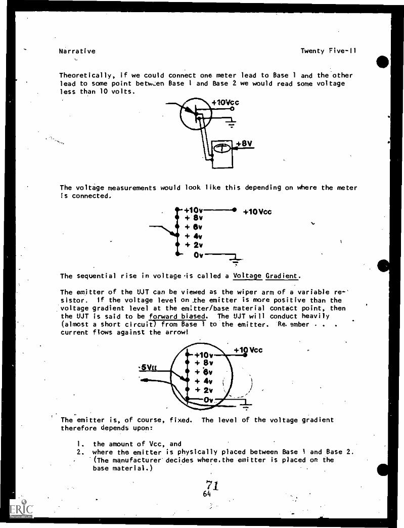
Theoretically, if we could connect one meter lead to Base 1 and the otherlead to some point betw,en Base 1 and Base 2 we would read some voltageless than 10 volts.
The voltage measurements would look like this depending on where the meteris connected.
That. +10v- +10Vcc+ 8v+ ev+ 4v+ 2v°v-a...
The sequential rise in voltageis called a Voltage Gradient.
The emitter of the OJT can be viewed as the wiper arm of a variable re-'sistor. If the voltage level on the emitter is more positive than thevoltage gradient level at the emitter /base material contact point, thenthe OJT is said to be forward biased. The OJT will conduct heavily(almost a short circuii171:Fii7471 to the emitter. Re.amber . .
current flows against the arrow!
The emitter is, of course, fixed. The level of the voltage gradienttherefore depends upon:
1. the amount of Vcc, and2. where the emitter is physically placed between Base I and Base 2.
(The manufacturer decides wherethe emitter is placed on thebase material.)
71
7
6
Narrative Twenty Five-II
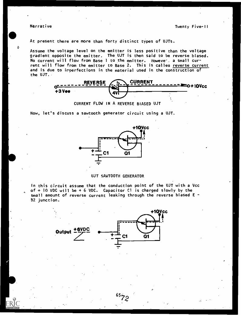
At present there are more than forty distinct types of UJTs.
Assume the voltage level on the emitter is less positive than the voltagegradient opposite the emitter. The UJT is then said to be reverse biased.No current will flow from Base 1 to the emitter. However. a small cur-rent will flow from the emitter to Base 2. This is calico reverse currentand is due to irperfections in the material used in the construction ofthe UJT.
REVERSE0+3 Vee
CURRENT11"-o+10Vcc
CURRENT FLOW IN A REVERSE BIASED UJT
Now, let's discuss a sawtooth generator circuit using a UJT.
UJT SAWTOOTH GENERATOR
In this circuit assume that the conduction point of the UJT with a Vccof 10 VDC will be 6 VDC. Capacitor Cl is charged slowly by thesmall amount of reverse current leaking through the reverse biased E -132. junction.
Output +6VDC-
65

Narrative Twerity Five-11
As the charge on Cl rises slowly through the high resistance of the E-B2junction it eventually reaches the level needed to forward bias the E-B1junction (+ 6 VDC).
+61/DCOutput ---7c
Cis DISCHARGE PATH
When the charge on Cl reaches the + 6 VDC conduction point of the UJT,the UJT "turns on" creating a low resistance discharge path for Cl throughthe now forward biased E - Bl junction. As Cl discharges, the voltagelevel on the emitter drops to OV causing the UJT to again become reversebiased and turn off. The cycle then starts all over.
The period of the waveform is determined by the resistance of the E-B2junction and the capacitance of Cl. (The junction resistance can bemeasured with a VOM.) The waveform produced looks like a sawtooth --hence, thename sawtooth generator.
. ,
61/
Ov
SAWTOOTH GENERATOR OUTPUT
,
a
7366

Narrative Twenty Five-II
We saw earlier in this lesson that the UJT can be used in several typesof circuits. Obviously, to explain them all would take too much time.The two most commonly used UJT circuits are the sawtooth generator (whichhas been discussed) and the multivibrator. Let's discuss the multivibra-tor.
TP
TP-BrV TIME-0-
11/1
lihME
WAVEFORMS SHOWINGWHAT IS HAPPENINGDURING THE TIME ClIS CHARGING.
+Vcc
TP
C1
- -
UJT MULTIV1BRATOR
R3OutputTP0
In the circuit shown, capacitor Cl charges through CR1 and R2. While CR1
is conducting, Q1 is cut off due to the low voltage level on the emitter.
11 T1 2
UM'
. Tree sR3
1
Trig. 1
+Vc c
TPtr
i C',11
i
o
o
[
,
1
a
1
TP"C"
At time Tl, Cl's charge (TP"A") becomes equal to the voltage level re-quired to forward bias Ql. Ql then turns on causing the voltage levelat TP"B" to drop to near ground potential -- zero volts. TP"C" (theoutput of the multivibrator) drops to near ground also.
6774
C
Narrative Twenty Five-11
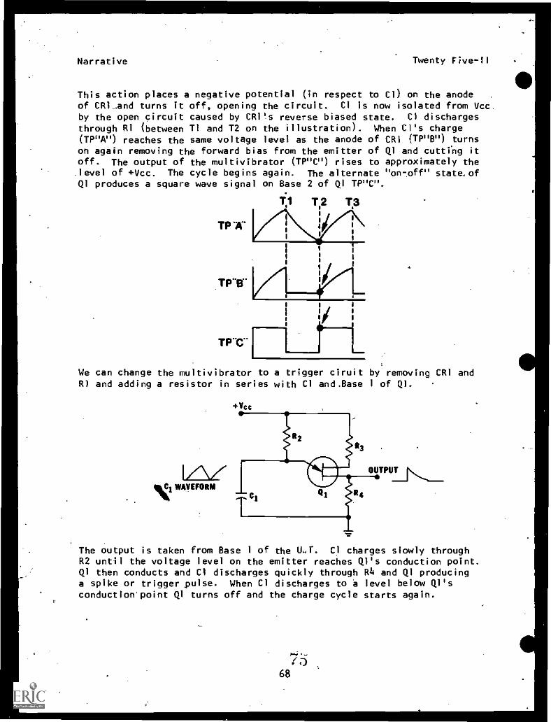
This action places a negative potential (in respect to Cl) on the anodeof CRl_and turns it off, opening the circuit. Cl is now isolated from Vcc.by the open circuit caused by CR1's reverse biased state. CI dischargesthrough RI (between T1 and T2 on the illustration). When Cl's charge(TP"A") reaches the same voltage level as the anode of CR1 (TP"B") turnson again removing the forward bias from the emitter of Ql and cutting itoff. The output of the multivibrator (TP"C") rises to approximately the.level of -4-Vcc. The cycle begins again. The alternate "on-off" state. ofQ1 produces a square wave signal on Base 2 of Q1 TP"C".
TPA'
TP-E1
TP-C-
T.1 T 2 T3
f
4
We can change the multivibrator to a trigger ciruit by removing CR1 andRI and adding a resistor in series with Cl and.Base 1 of Ql.
LiZ41041 WAVEFORM
The output is taken from Base 1 of the U.T. Cl charges slowly throughR2 until the voltage level on the emitter reaches QI's conduction point.Ql then conducts and CI discharges quickly through R4 and Ql producinga spike or trigger pulse. When Cl discharges to a level below Ql'sconduction' point Q1 turns off and the charge cycle starts again.
.1-
. 68
t
.,
Narrative Twenty Five-II
---:-..
AT THIS POINT, YOU MAY TAKE THE LESSON PROGRESS CHECK. IF YOUANSWER ALL SELF-TEST ITEMS .CORRECTLY, PROCEED TO THE NEXT LESSON.IF YOU INCORRECTLY ANSWER ONLY A FEW OF THE PROGRESS CHECK QUESTIONS,THE CORRECT ANSWER PAGEWILL REFER YOU TO THE APPROPRIATE PAGES,PARAGRAPHS, OR FRAMES SO THAT YOU CAN RESTUDY THE PARTS OF THISLESSON YOU ARE HAVING DIFFICULTY WITH. IF YOU FEEL THAT YOU HAVEFAILED TO UNDERSTAND ALL, OR MOST, OF THE LESSON, SELECT AND USEANOTHER WRITTEN MEDIUM OF INSTRUCTION, AUOIO /VISUAL MATERIALS (IFAPPLICABLE), OR CONSULTATION WITH LEARNING SUPERVISOR, UNTIL YOUCAN ANSWER ALL SELF-TEST ITEMS ON THE PROGRESS CHECK CORRECTLY.
76 *
69
I.,