bq24076, bq24078 datasheet - texas instruments · pulled down with approximately 285 kΩ. do not...
TRANSCRIPT
IN
VSS
BAT
bq24076bq24078
OUT
EN2
TSTEMP
PACK+
PACK-
SYSTEM
SYSOFFSystemON/OFFControl
IN13
8
15
4 14 6 12 16
1
2
3
5
10
11
97
1 Fm
4.7 Fm
4.7 Fm
1.13kW1.18kW
1kW
1kW
PG
OO
D
CH
G
EN
1
ILM
CE
TM
R
ISE
T
Copyright © 2017, Texas Instruments Incorporated
Product
Folder
Order
Now
Technical
Documents
Tools &
Software
Support &Community
An IMPORTANT NOTICE at the end of this data sheet addresses availability, warranty, changes, use in safety-critical applications,intellectual property matters and other important disclaimers. PRODUCTION DATA.
bq24076, bq24078SLUSCM1A –OCTOBER 2017–REVISED DECEMBER 2017
bq2407x 1.5-A High Battery Voltage Li-Ion Battery Chargerswith Power-Path Management IC
1
1 Features1• Fully Compliant USB Charger
– Selectable 100-mA and 500-mA MaximumInput Current
– 100-mA Maximum Current Limit EnsuresCompliance to USB-IF Standard
– Input-Based Dynamic Power Management(VIN-DPM) for Protection Against Poor USBSources
• 28-V Input Rating with Overvoltage Protection• Integrated Dynamic Power Path Management
(DPPM) Function Simultaneously andIndependently Powers the System and Chargesthe Battery
• Supports up to 1.5-A Charge Current with CurrentMonitoring Output (ISET)
• Programmable Input Current Limit up to 1.5 A forWall Adapters
• System Output Tracks Battery Voltage• Battery Disconnect Function with SYSOFF Input• Programmable Pre-Charge and Fast-Charge
Safety Timers• Reverse Current, Short-Circuit, and Thermal
Protection• NTC Thermistor Input• Proprietary Start-up Sequence Limits Inrush
Current• Battery Charge Voltage, VBAT:
– bq24076 - 4.4 V (typ)– bq24078 - 4.35 V (typ)
• Status Indication – Charging/Done, Power Good
2 Applications• Smart Phones• Portable Media Players• Portable Navigation Devices• Low-Power Handheld Devices• Portable Gaming• Headsets• Wearables• Home Automation• Portable Medical
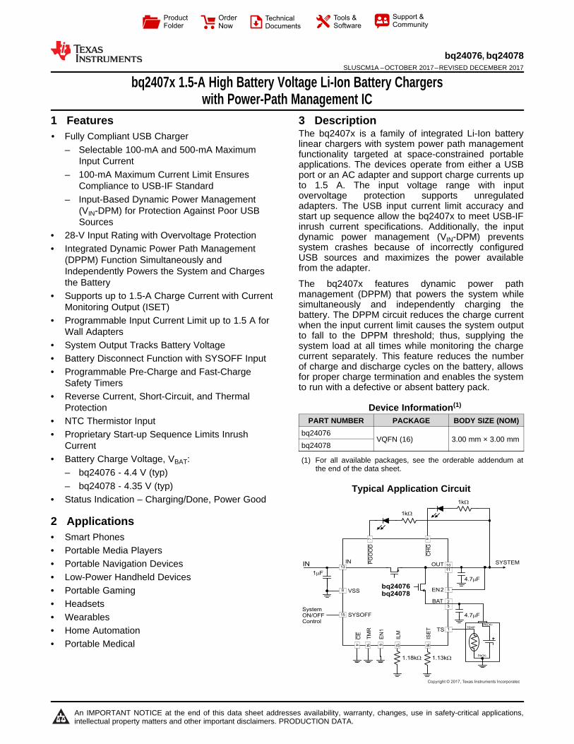
3 DescriptionThe bq2407x is a family of integrated Li-Ion batterylinear chargers with system power path managementfunctionality targeted at space-constrained portableapplications. The devices operate from either a USBport or an AC adapter and support charge currents upto 1.5 A. The input voltage range with inputovervoltage protection supports unregulatedadapters. The USB input current limit accuracy andstart up sequence allow the bq2407x to meet USB-IFinrush current specifications. Additionally, the inputdynamic power management (VIN-DPM) preventssystem crashes because of incorrectly configuredUSB sources and maximizes the power availablefrom the adapter.
The bq2407x features dynamic power pathmanagement (DPPM) that powers the system whilesimultaneously and independently charging thebattery. The DPPM circuit reduces the charge currentwhen the input current limit causes the system outputto fall to the DPPM threshold; thus, supplying thesystem load at all times while monitoring the chargecurrent separately. This feature reduces the numberof charge and discharge cycles on the battery, allowsfor proper charge termination and enables the systemto run with a defective or absent battery pack.
Device Information(1)
PART NUMBER PACKAGE BODY SIZE (NOM)bq24076
VQFN (16) 3.00 mm × 3.00 mmbq24078
(1) For all available packages, see the orderable addendum atthe end of the data sheet.
Typical Application Circuit

2
bq24076, bq24078SLUSCM1A –OCTOBER 2017–REVISED DECEMBER 2017 www.ti.com
Product Folder Links: bq24076 bq24078
Submit Documentation Feedback Copyright © 2017, Texas Instruments Incorporated
Table of Contents1 Features .................................................................. 12 Applications ........................................................... 13 Description ............................................................. 14 Revision History..................................................... 25 Description (continued)......................................... 36 Device Comparison Table ..................................... 37 Pin Configuration and Functions ......................... 48 Specifications......................................................... 5
8.1 Absolute Maximum Ratings ..................................... 58.2 ESD Ratings.............................................................. 58.3 Recommended Operating Conditions....................... 68.4 Thermal Information .................................................. 68.5 Dissipation Ratings ................................................... 68.6 Electrical Characteristics........................................... 78.7 Typical Characteristics .............................................. 9
9 Detailed Description ............................................ 119.1 Overview ................................................................. 119.2 Functional Block Diagram ....................................... 129.3 Feature Description................................................. 13
9.4 Device Functional Modes........................................ 2410 Application and Implementation........................ 26
10.1 Application Information.......................................... 2610.2 Typical Application ................................................ 26
11 Power Supply Recommendations ..................... 3112 Layout................................................................... 31
12.1 Layout Guidelines ................................................. 3112.2 Layout Example .................................................... 3212.3 Thermal Considerations ........................................ 33
13 Device and Documentation Support ................. 3413.1 Device Support...................................................... 3413.2 Related Links ........................................................ 3413.3 Receiving Notification of Documentation Updates 3413.4 Community Resources.......................................... 3413.5 Trademarks ........................................................... 3413.6 Electrostatic Discharge Caution............................ 3413.7 Glossary ................................................................ 34
14 Mechanical, Packaging, and OrderableInformation ........................................................... 34
4 Revision History
Changes from Original (October 2017) to Revision A Page
• Changed IIN Test Conditions From: TJ = 85°C To: TJ < 85°C in the Electrical Characteristics table ..................................... 7
3
bq24076, bq24078www.ti.com SLUSCM1A –OCTOBER 2017–REVISED DECEMBER 2017
Product Folder Links: bq24076 bq24078
Submit Documentation FeedbackCopyright © 2017, Texas Instruments Incorporated
5 Description (continued)Additionally, the regulated system input enables instant system turn-on when plugged in even with a totallydischarged battery. The power-path management architecture also lets the battery supplement the systemcurrent requirements when the adapter cannot deliver the peak system currents, thus enabling the use of asmaller adapter.
The battery is charged in three phases: conditioning, constant current, and constant voltage. In all chargephases, an internal control loop monitors the IC junction temperature and reduces the charge current if theinternal temperature threshold is exceeded. The charger power stage and charge current sense functions arefully integrated. The charger function has high accuracy current and voltage regulation loops, charge statusdisplay, and charge termination. The input current limit and charge current are programmable using externalresistors.
(1) For all available packages, see the orderable addendum at the end of the data sheet(2) This product is RoHS compatible, including a lead concentration that does not exceed 0.1% of total product weight, and is suitable for
use in specified lead-free soldering processes. In addition, this product uses package materials that do not contain halogens, includingbromine (Br) or antimony (Sb) above 0.1% of total product weight.
6 Device Comparison Table
PART NUMBER (1) (2) VOVP VBAT(REG) VOUT(REG) VDPPMOPTIONALFUNCTION
bq24072 6.6 V 4.2 V VBAT + 225 mV VO(REG) – 100 mV TDbq24073 6.6 V 4.2 V 4.4 V VO(REG) – 100 mV TDbq24074 10.5 V 4.2 V 4.4 V VO(REG) – 100 mV ITERMbq24075 6.6 V 4.2 V 5.5 V 4.3 V SYSOFFbq24076 6.6 V 4.4 V VBAT + 210mV VBAT +100 mV SYSOFFbq24078 6.6 V 4.35 V VBAT + 210mV VBAT +100 mV SYSOFFbq24079 6.6 V 4.1 V 5.5 V 4.3 V SYSOFF
16IS
ET
5E
N2
1TS 12 ILIM
15S
YS
OF
F6
EN
1
2BAT 11 OUT
14T
MR
7P
GO
OD
3BAT 10 OUT
13IN
8V
SS
4CE 9 CHG
Not to scale
Thermal
Pad
4
bq24076, bq24078SLUSCM1A –OCTOBER 2017–REVISED DECEMBER 2017 www.ti.com
Product Folder Links: bq24076 bq24078
Submit Documentation Feedback Copyright © 2017, Texas Instruments Incorporated
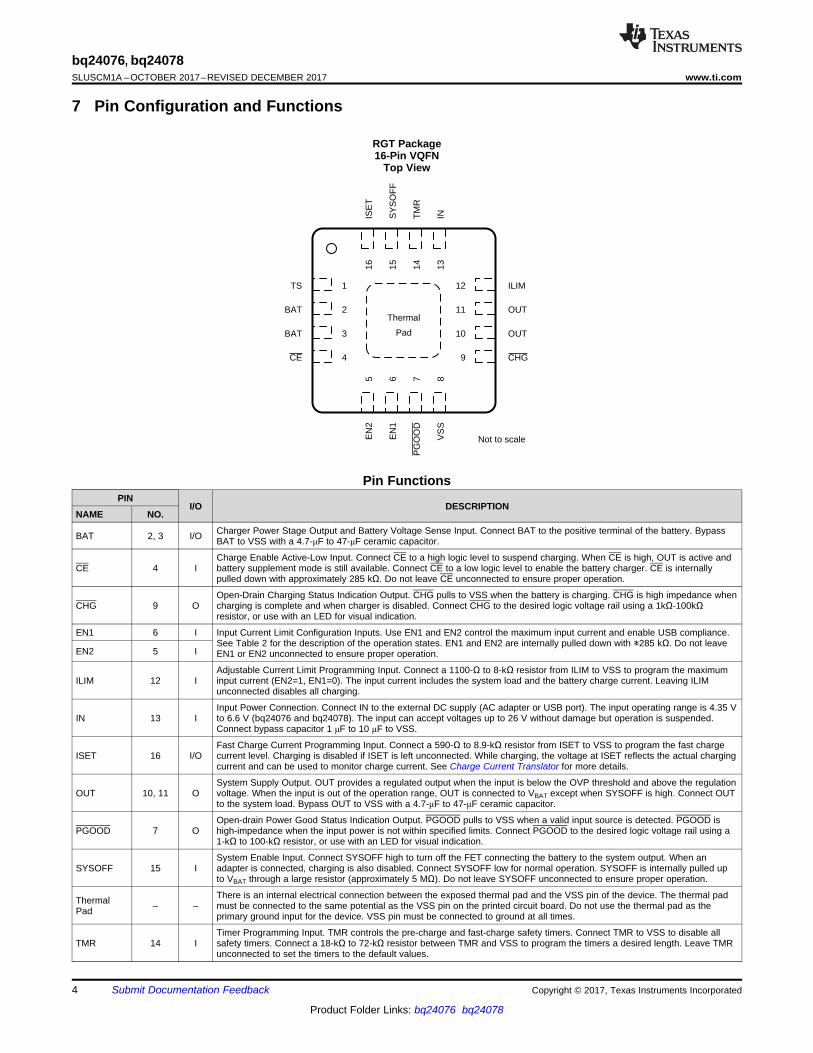
7 Pin Configuration and Functions
RGT Package16-Pin VQFN
Top View
Pin FunctionsPIN
I/O DESCRIPTIONNAME NO.
BAT 2, 3 I/O Charger Power Stage Output and Battery Voltage Sense Input. Connect BAT to the positive terminal of the battery. BypassBAT to VSS with a 4.7-μF to 47-μF ceramic capacitor.
CE 4 ICharge Enable Active-Low Input. Connect CE to a high logic level to suspend charging. When CE is high, OUT is active andbattery supplement mode is still available. Connect CE to a low logic level to enable the battery charger. CE is internallypulled down with approximately 285 kΩ. Do not leave CE unconnected to ensure proper operation.
CHG 9 OOpen-Drain Charging Status Indication Output. CHG pulls to VSS when the battery is charging. CHG is high impedance whencharging is complete and when charger is disabled. Connect CHG to the desired logic voltage rail using a 1kΩ-100kΩresistor, or use with an LED for visual indication.
EN1 6 I Input Current Limit Configuration Inputs. Use EN1 and EN2 control the maximum input current and enable USB compliance.See Table 2 for the description of the operation states. EN1 and EN2 are internally pulled down with ≉285 kΩ. Do not leaveEN1 or EN2 unconnected to ensure proper operation.EN2 5 I
ILIM 12 IAdjustable Current Limit Programming Input. Connect a 1100-Ω to 8-kΩ resistor from ILIM to VSS to program the maximuminput current (EN2=1, EN1=0). The input current includes the system load and the battery charge current. Leaving ILIMunconnected disables all charging.
IN 13 IInput Power Connection. Connect IN to the external DC supply (AC adapter or USB port). The input operating range is 4.35 Vto 6.6 V (bq24076 and bq24078). The input can accept voltages up to 26 V without damage but operation is suspended.Connect bypass capacitor 1 μF to 10 μF to VSS.
ISET 16 I/OFast Charge Current Programming Input. Connect a 590-Ω to 8.9-kΩ resistor from ISET to VSS to program the fast chargecurrent level. Charging is disabled if ISET is left unconnected. While charging, the voltage at ISET reflects the actual chargingcurrent and can be used to monitor charge current. See Charge Current Translator for more details.
OUT 10, 11 OSystem Supply Output. OUT provides a regulated output when the input is below the OVP threshold and above the regulationvoltage. When the input is out of the operation range, OUT is connected to VBAT except when SYSOFF is high. Connect OUTto the system load. Bypass OUT to VSS with a 4.7-μF to 47-μF ceramic capacitor.
PGOOD 7 OOpen-drain Power Good Status Indication Output. PGOOD pulls to VSS when a valid input source is detected. PGOOD ishigh-impedance when the input power is not within specified limits. Connect PGOOD to the desired logic voltage rail using a1-kΩ to 100-kΩ resistor, or use with an LED for visual indication.
SYSOFF 15 ISystem Enable Input. Connect SYSOFF high to turn off the FET connecting the battery to the system output. When anadapter is connected, charging is also disabled. Connect SYSOFF low for normal operation. SYSOFF is internally pulled upto VBAT through a large resistor (approximately 5 MΩ). Do not leave SYSOFF unconnected to ensure proper operation.
ThermalPad – –
There is an internal electrical connection between the exposed thermal pad and the VSS pin of the device. The thermal padmust be connected to the same potential as the VSS pin on the printed circuit board. Do not use the thermal pad as theprimary ground input for the device. VSS pin must be connected to ground at all times.
TMR 14 ITimer Programming Input. TMR controls the pre-charge and fast-charge safety timers. Connect TMR to VSS to disable allsafety timers. Connect a 18-kΩ to 72-kΩ resistor between TMR and VSS to program the timers a desired length. Leave TMRunconnected to set the timers to the default values.
5
bq24076, bq24078www.ti.com SLUSCM1A –OCTOBER 2017–REVISED DECEMBER 2017
Product Folder Links: bq24076 bq24078
Submit Documentation FeedbackCopyright © 2017, Texas Instruments Incorporated
Pin Functions (continued)PIN
I/O DESCRIPTIONNAME NO.
TS 1 IExternal NTC Thermistor Input. Connect the TS input to the NTC thermistor in the battery pack. TS monitors a 10-kΩ NTCthermistor. For applications that do not use the TS function, connect a 10-kΩ fixed resistor from TS to VSS to maintain a validvoltage level on TS.
VSS 8 – Ground. Connect to the thermal pad and to the ground rail of the circuit.
Table 1. EN1/EN2 SettingsEN2 EN1 MAXIMUM INPUT CURRENT INTO IN PIN
0 0 100 mA. USB100 mode0 1 500 mA. USB500 mode1 0 Set by an external resistor from ILIM to VSS1 1 Standby (USB suspend mode)
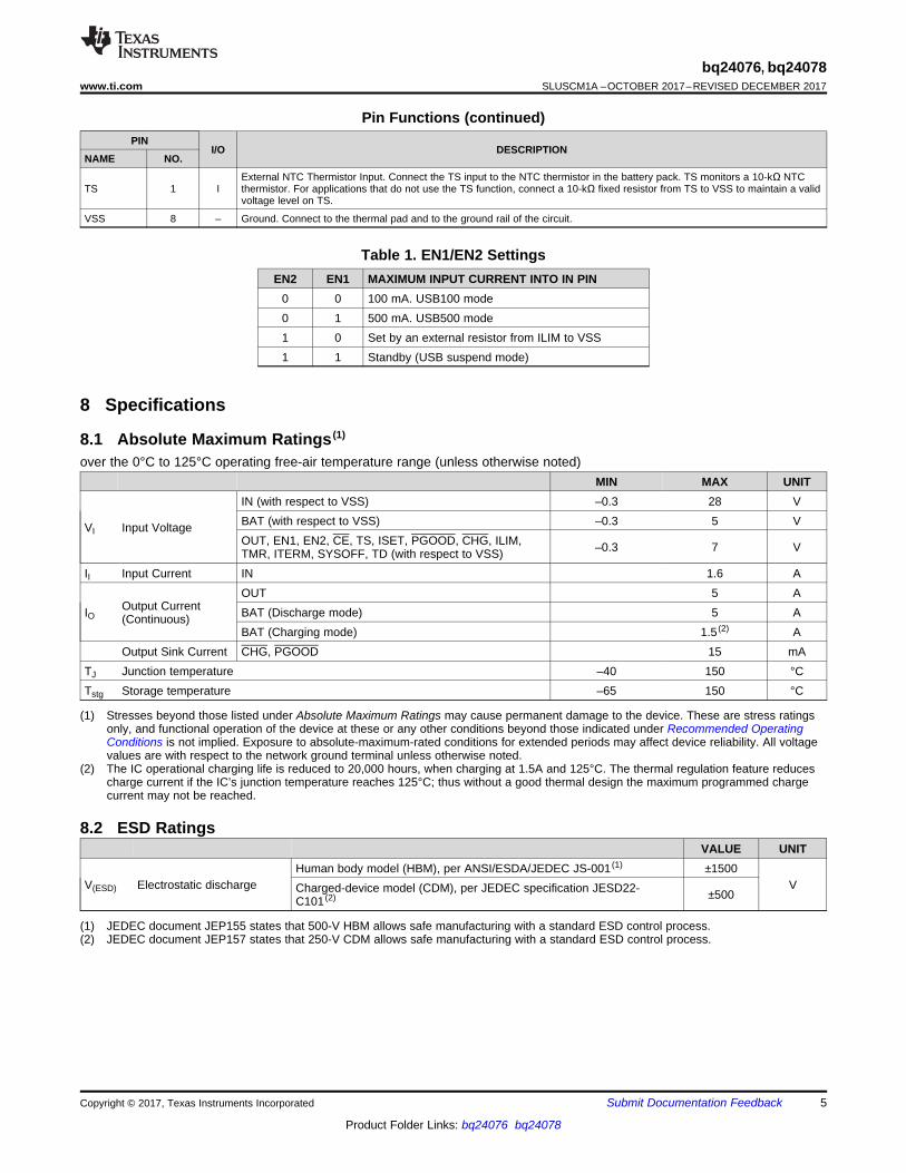
(1) Stresses beyond those listed under Absolute Maximum Ratings may cause permanent damage to the device. These are stress ratingsonly, and functional operation of the device at these or any other conditions beyond those indicated under Recommended OperatingConditions is not implied. Exposure to absolute-maximum-rated conditions for extended periods may affect device reliability. All voltagevalues are with respect to the network ground terminal unless otherwise noted.
(2) The IC operational charging life is reduced to 20,000 hours, when charging at 1.5A and 125°C. The thermal regulation feature reducescharge current if the IC’s junction temperature reaches 125°C; thus without a good thermal design the maximum programmed chargecurrent may not be reached.
8 Specifications
8.1 Absolute Maximum Ratings (1)
over the 0°C to 125°C operating free-air temperature range (unless otherwise noted)MIN MAX UNIT
VI Input Voltage
IN (with respect to VSS) –0.3 28 VBAT (with respect to VSS) –0.3 5 VOUT, EN1, EN2, CE, TS, ISET, PGOOD, CHG, ILIM,TMR, ITERM, SYSOFF, TD (with respect to VSS) –0.3 7 V
II Input Current IN 1.6 A
IOOutput Current(Continuous)
OUT 5 ABAT (Discharge mode) 5 ABAT (Charging mode) 1.5 (2) A
Output Sink Current CHG, PGOOD 15 mATJ Junction temperature –40 150 °CTstg Storage temperature –65 150 °C
(1) JEDEC document JEP155 states that 500-V HBM allows safe manufacturing with a standard ESD control process.(2) JEDEC document JEP157 states that 250-V CDM allows safe manufacturing with a standard ESD control process.
8.2 ESD RatingsVALUE UNIT
V(ESD) Electrostatic dischargeHuman body model (HBM), per ANSI/ESDA/JEDEC JS-001 (1) ±1500
VCharged-device model (CDM), per JEDEC specification JESD22-C101 (2) ±500
6
bq24076, bq24078SLUSCM1A –OCTOBER 2017–REVISED DECEMBER 2017 www.ti.com
Product Folder Links: bq24076 bq24078
Submit Documentation Feedback Copyright © 2017, Texas Instruments Incorporated
(1) The IC operational charging life is reduced to 20,000 hours, when charging at 1.5A and 125°C. The thermal regulation feature reducescharge current if the IC’s junction temperature reaches 125°C; thus without a good thermal design the maximum programmed chargecurrent may not be reached.
(2) Use a 1% tolerance resistor for RISET to avoid issues with the RISET short test when using the maximum charge current setting.
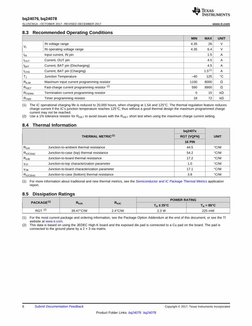
8.3 Recommended Operating ConditionsMIN MAX UNIT
VIIN voltage range 4.35 26 VIN operating voltage range 4.35 6.4 V
IIN Input current, IN pin 1.5 AIOUT Current, OUT pin 4.5 AIBAT Current, BAT pin (Discharging) 4.5 AICHG Current, BAT pin (Charging) 1.5 (1) ATJ Junction Temperature –40 125 °CRILIM Maximum input current programming resistor 1100 8000 ΩRISET Fast-charge current programming resistor (2) 590 8900 ΩRITERM Termination current programming resistor 0 15 kΩRTMR Timer programming resistor 18 72 kΩ
(1) For more information about traditional and new thermal metrics, see the Semiconductor and IC Package Thermal Metrics applicationreport.
8.4 Thermal Information
THERMAL METRIC (1)bq2407x
UNITRGT (VQFN)16 PIN
RθJA Junction-to-ambient thermal resistance 44.5 °C/WRθJC(top) Junction-to-case (top) thermal resistance 54.2 °C/WRθJB Junction-to-board thermal resistance 17.2 °C/WψJT Junction-to-top characterization parameter 1.0 °C/WψJB Junction-to-board characterization parameter 17.1 °C/WRθJC(bot) Junction-to-case (bottom) thermal resistance 3.8 °C/W
(1) For the most current package and ordering information, see the Package Option Addendum at the end of this document, or see the TIwebsite at www.ti.com.
(2) This data is based on using the JEDEC High-K board and the exposed die pad is connected to a Cu pad on the board. The pad isconnected to the ground plane by a 2 × 3 via matrix.
8.5 Dissipation Ratings
PACKAGE (1) RθJA RθJCPOWER RATING
TA ≤ 25°C TA = 85°CRGT (2) 39.47°C/W 2.4°C/W 2.3 W 225 mW
7
bq24076, bq24078www.ti.com SLUSCM1A –OCTOBER 2017–REVISED DECEMBER 2017
Product Folder Links: bq24076 bq24078
Submit Documentation FeedbackCopyright © 2017, Texas Instruments Incorporated
8.6 Electrical CharacteristicsOver junction temperature range (0° ≤ TJ ≤ 125°C) and the recommended supply voltage range (unless otherwise noted)
PARAMETER TEST CONDITIONS MIN TYP MAX UNIT
INPUT
UVLO Undervoltage lock-out VIN: 0 V → 4 V 3.2 3.3 3.4 V
Vhys Hysteresis on UVLO VIN: 4 V → 0 V 200 300 mV
VIN(DT) Input power detection thresholdInput power detected when VIN > VBAT + VIN(DT)
VBAT = 3.6 V, VIN: 3.5 V → 4 V55 80 130 mV
Vhys Hysteresis on VIN(DT) VBAT = 3.6 V, VIN: 4 V → 3.5 V 20 mV
tDGL(PGOOD) Deglitch time, input power detected statusTime measured from VIN: 0 V → 5 V 1 μsrise-time to PGOOD = LO
1.2 ms
VOVP Input overvoltage protection threshold VIN: 5 V → 7 V 6.4 6.6 6.8 V
Vhys Hysteresis on OVP VIN: 7 V → 5V 110 mV
tDGL(OVP) Input overvoltage blanking time (OVP fault deglitch) 50 μs
tREC Input overvoltage recovery timeTime measured from VIN: 11 V → 5 V with 1 μsfall-time to PGOOD = LO
1.2 ms
ILIM, ISET SHORT-CIRCUIT DETECTION (CHECKED DURING STARTUP)
ISC Current source VIN > UVLO and VIN > VBAT + VIN(DT) 1.3 mA
VSC VIN > UVLO and VIN > VBAT + VIN(DT) 520 mV
QUIESCENT CURRENT
IBAT(PDWN) Sleep current into BAT pin CE = LO or HI, input power not detected,No load on OUT pin, TJ = 85°C 4.1 7 μA
IIN Standby current into IN pinEN1= HI, EN2=HI, VIN = 6 V, TJ < 85°C 39 50
μAEN1= HI, EN2=HI, VIN = 10 V, TJ < 85°C 91 200
ICC Active supply current, IN pinCE = LO, VIN = 6 V, no load on OUT pin,VBAT > VBAT(REG), (EN1, EN2) ≠ (HI, HI)
1.5 mA
POWER PATH
VDO(IN-OUT) VIN – VOUT VIN = 4.3 V, IIN = 1 A, VBAT = 4.2 V 300 475 mV
VDO(BAT-OUT) VBAT – VOUT IOUT = 1 A, VIN = 0 V, VBAT > 3 V 50 100 mV
VO(REG) OUT pin voltage regulationVIN > VOUT + VDO(IN-OUT), VBAT < 3.2 V 3.31 3.41 3.51
VVIN > VOUT + VDO(IN-OUT), VBAT ≥ 3.2 V VBAT +
145mVVBAT +
210mVVBAT +
275mV
IINmax Maximum input current
EN1 = LO, EN2 = LO 90 95 100mA
EN1 = HI, EN2 = LO 450 475 500
EN2 = HI, EN1 = LO KILIM/RILIM A
KILIM Maximum input current factorILIM = 500 mA to 1.5 A 1500 1610 1720
AΩILIM = 200 mA to 500 mA 1330 1525 1720
IINmax Programmable input current limit range EN2 = HI, EN1 = LO, RILIM = 8 kΩ to 1.1 kΩ 200 1500 mA
VIN-DPMInput voltage threshold when input current isreduced EN2 = LO, EN1 = X 4.35 4.5 4.63 V
VDPPMOutput voltage threshold when charging current isreduced
VBAT +125mV
VBAT +100mV
VBAT +85mV V
VBSUP1 Enter battery supplement mode VBAT = 3.6 V, RILIM = 1.5 kΩ, RLOAD = 10 Ω → 2 Ω VOUT ≤ VBAT–40mV V
VBSUP2 Exit battery supplement mode VBAT = 3.6 V, RILIM = 1.5 kΩ, RLOAD = 2 Ω → 10 Ω VOUT ≥VBAT–20mV V
VO(SC1) Output short-circuit detection threshold, power-on VIN > VUVLO and VIN > VBAT + VIN(DT) 0.8 0.9 1 V
VO(SC2)Output short-circuit detection threshold, supplementmode VBAT – VOUT > VO(SC2) indicates short-circuit VIN > VUVLO and VIN > VBAT + VIN(DT) 200 250 300 mV
tDGL(SC2) Deglitch time, supplement mode short circuit 250 μs
tREC(SC2) Recovery time, supplement mode short circuit 60 ms
BATTERY CHARGER
IBAT Source current for BAT pin short-circuit detection VBAT = 1.5 V 4 7.5 11 mA
VBAT(SC) BAT pin short-circuit detection threshold VBAT rising 1.6 1.8 2 V
VBAT(REG) Battery charge voltage('76) 4.358 4.4 4.44
V('78) 4.31 4.35 4.39
VLOWV Pre-charge to fast-charge transition threshold VIN > VUVLO and VIN > VBAT + VIN(DT) 2.9 3 3.1 V
tDGL1(LOWV) Deglitch time on pre-charge to fast-charge transition 25 ms
tDGL2(LOWV) Deglitch time on fast-charge to pre-charge transition 25 ms
8
bq24076, bq24078SLUSCM1A –OCTOBER 2017–REVISED DECEMBER 2017 www.ti.com
Product Folder Links: bq24076 bq24078
Submit Documentation Feedback Copyright © 2017, Texas Instruments Incorporated
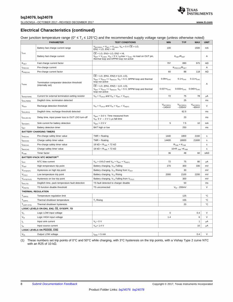
Electrical Characteristics (continued)Over junction temperature range (0° ≤ TJ ≤ 125°C) and the recommended supply voltage range (unless otherwise noted)
PARAMETER TEST CONDITIONS MIN TYP MAX UNIT
(1) These numbers set trip points of 0°C and 50°C while charging, with 3°C hysteresis on the trip points, with a Vishay Type 2 curve NTCwith an R25 of 10 kΩ.
ICHG
Battery fast charge current range VBAT(REG) > VBAT > VLOWV, VIN = 5 V CE = LO,EN1 = LO, EN2 = HI 100 1500 mA
Battery fast charge currentCE = LO, EN1= LO, EN2 = HI,VBAT > VLOWV, VIN = 5 V, IINmax > ICHG, no load on OUT pin,thermal loop and DPPM loop not active
KISET/RISET A
KISET Fast charge current factor 797 890 975 AΩ
IPRECHG Pre-charge current KPRECHG/RISET A
KPRECHG Pre-charge current factor 60 88 118 AΩ
ITERMTermination comparator detection threshold(internally set)
CE = LO, (EN1, EN2) ≠ (LO, LO),VBAT > VRCH, t < tMAXCH, VIN = 5 V, DPPM loop and thermalloop not active
0.09×ICHG 0.1×ICHG 0.11×ICHG
ACE = LO, (EN1, EN2) = (LO, LO),VBAT > VRCH, t < tMAXCH, VIN = 5 V, DPPM loop and thermalloop not active
0.027×ICHG 0.033×ICHG 0.040×ICHG
IBIAS(ITERM) Current for external termination-setting resistor VIN > VUVLO and VIN > VBAT + VIN(DT) 72 75 78 μA
tDGL(TERM) Deglitch time, termination detected 25 ms
VRCH Recharge detection threshold VIN > VUVLO and VIN > VBAT + VIN(DT)VBAT(REG)–140mV
VBAT(REG)–100mV
VBAT(REG)–60mV V
tDGL(RCH) Deglitch time, recharge threshold detected 62.5 ms
tDGL(NO-IN) Delay time, input power loss to OUT LDO turn-offVBAT = 3.6 V. Time measured fromVIN: 5 V → 3 V 1 μs fall-time
20 ms
IBAT(DET) Sink current for battery detection VBAT = 2.5 V 5 7.5 10 mA
tDET Battery detection timer BAT high or low 250 ms
BATTERY CHARGING TIMERS
tPRECHG Pre-charge safety timer value TMR = floating 1440 1800 2160 s
tMAXCHG Charge safety timer value TMR = floating 14400 18000 21600 s
tPRECHG Pre-charge safety timer value 18 kΩ < RTMR < 72 kΩ RTMR × KTMR s
tMAXCHG Charge safety timer value 18 kΩ < RTMR < 72 kΩ 10×R TMR ×KTMR s
KTMR Timer factor 36 48 60 s/kΩ
BATTERY-PACK NTC MONITOR (1)
INTC NTC bias current VIN > UVLO and VIN > VBAT + VIN(DT) 72 75 80 μA
VHOT High temperature trip point Battery charging, VTS Falling 270 300 330 mV
VHYS(HOT) Hysteresis on high trip point Battery charging, VTS Rising from VHOT 30 mV
VCOLD Low temperature trip point Battery charging, VTS Rising 2000 2100 2200 mV
VHYS(COLD) Hysteresis on low trip point Battery charging, VTS Falling from VCOLD 300 mV
tDGL(TS) Deglitch time, pack temperature fault detection TS fault detected to charger disable 50 ms
VDIS(TS) TS function disable threshold TS unconnected VIN - 200mV V
THERMAL REGULATION
TJ(REG) Temperature regulation limit 125 °C
TJ(OFF) Thermal shutdown temperature TJ Rising 155 °C
TJ(OFF-HYS) Thermal shutdown hysteresis 20 °C
LOGIC LEVELS ON EN1, EN2, CE, SYSOFF, TD
VIL Logic LOW input voltage 0 0.4 V
VIH Logic HIGH input voltage 1.4 6 V
IIL Input sink current VIL= 0 V 1 μA
IIH Input source current VIH= 1.4 V 10 μA
LOGIC LEVELS ON PGOOD, CHG
VOL Output LOW voltage ISINK = 5 mA 0.4 V
3.60
3.62
3.64
3.66
3.68
3.70
3.72
3.74
3.76
3.78
3.80
0 25 50 75 100 125
Junction Temperature (°C)
V-
Ou
tpu
t V
olt
ag
e (
V)
O
4.30
4.33
4.35
4.38
4.40
4.43
4.45
0 25 50 75 100 125
Junction Temperature (°C)
V-
Ou
tpu
t V
olt
ag
e (
V)
O
0
20
40
60
80
100
120
0 25 50 75 100 125
Junction Temperature (°C)
Dro
po
ut
Vo
lta
ge
(V
- V
BA
TO
UT)
VBAT = 3 V
VBAT = 3.9 V
3
3.2
3.4
3.6
3.8
4
4.2
4.4
4.6
V-
Ou
tpu
t V
olt
ag
e (
V)
O
2 2.5 3 3.5 4 4.5
V - Battery Voltage (V)BAT
600
400
100
Temperature ( C)o
300
200
500
0120 125 130 135 140 145
I(m
A)
BA
T
0
0.1
0.2
0.3
0.4
0.5
0.6
0.7
0 25 50 75 100 125
Junction Temperature (°C)
Dro
po
ut
Vo
lta
ge
(V
- V
INO
UT)
9
bq24076, bq24078www.ti.com SLUSCM1A –OCTOBER 2017–REVISED DECEMBER 2017
Product Folder Links: bq24076 bq24078
Submit Documentation FeedbackCopyright © 2017, Texas Instruments Incorporated
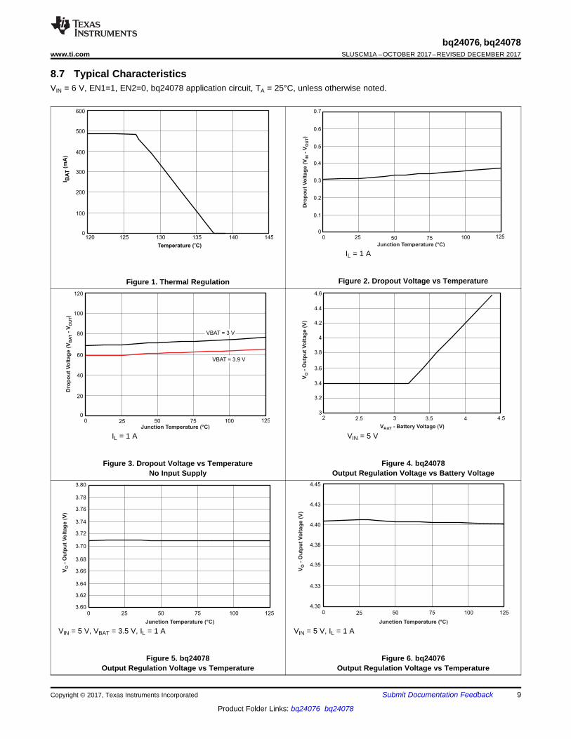
8.7 Typical CharacteristicsVIN = 6 V, EN1=1, EN2=0, bq24078 application circuit, TA = 25°C, unless otherwise noted.
Figure 1. Thermal Regulation
IL = 1 A
Figure 2. Dropout Voltage vs Temperature
IL = 1 A
Figure 3. Dropout Voltage vs TemperatureNo Input Supply
VIN = 5 V
Figure 4. bq24078Output Regulation Voltage vs Battery Voltage
VIN = 5 V, VBAT = 3.5 V, IL = 1 A
Figure 5. bq24078Output Regulation Voltage vs Temperature
VIN = 5 V, IL = 1 A
Figure 6. bq24076Output Regulation Voltage vs Temperature
28.5
29
29.5
30
30.5
31
31.5
2 2.2 2.4 2.6 2.8 3
I-
BA
TP
rech
arg
e C
urr
en
t (m
A)
V -BAT Battery Voltage (V)
95
96
97
98
99
100
101
102
103
104
105
I-
Pre
ch
arg
e C
urr
en
t (A
)B
AT
2 2.2 2.4 2.6 2.8 3
V - Battery Voltage (V)BAT
280
285
290
295
300
305
310
3 3.2 3.4 3.6 3.8 4 4.2
I-
BA
TF
ast
Ch
arg
e C
urr
en
t (m
A)
V -BAT Battery Voltage (V)
0.95
0.97
0.99
1.01
1.03
1.05
3 3.2 3.4 3.6 3.8 4 4.2
Fa
st
Ch
arg
e C
urr
en
t (A
)I
-B
AT
V -BAT Battery Voltage (V)
6.45
6.50
6.55
6.60
6.65
6.70
0 25 50 75 100 125
Junction Temperature (°C)
V-
OV
PO
utp
ut
Vo
lta
ge
Th
res
ho
ld (
V)
V RisingI
V FallingI
4.200
4.250
4.300
4.350
4.400
4.450
4.500
0 5 10 15 20 25 30
Junction Temperature (°C)
V-
Reg
ula
tio
n V
olt
ag
e (
V)
BA
T
10
bq24076, bq24078SLUSCM1A –OCTOBER 2017–REVISED DECEMBER 2017 www.ti.com
Product Folder Links: bq24076 bq24078
Submit Documentation Feedback Copyright © 2017, Texas Instruments Incorporated
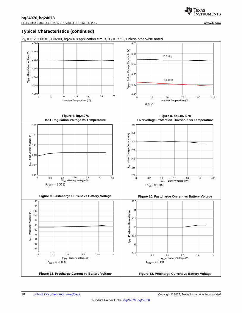
Typical Characteristics (continued)VIN = 6 V, EN1=1, EN2=0, bq24078 application circuit, TA = 25°C, unless otherwise noted.
Figure 7. bq24076BAT Regulation Voltage vs Temperature
6.6 V
Figure 8. bq24076/78Overvoltage Protection Threshold vs Temperature
RISET = 900 Ω
Figure 9. Fastcharge Current vs Battery Voltage
RISET = 3 kΩ
Figure 10. Fastcharge Current vs Battery Voltage
RISET = 900 Ω
Figure 11. Precharge Current vs Battery Voltage
RISET = 3 kΩ
Figure 12. Precharge Current vs Battery Voltage
11
bq24076, bq24078www.ti.com SLUSCM1A –OCTOBER 2017–REVISED DECEMBER 2017
Product Folder Links: bq24076 bq24078
Submit Documentation FeedbackCopyright © 2017, Texas Instruments Incorporated
9 Detailed Description
9.1 OverviewThe bq2407x devices are integrated Li-Ion linear chargers and system power path management devices targetedat space-limited portable applications. The device powers the system while simultaneously and independentlycharging the battery. This feature reduces the number of charge and discharge cycles on the battery, allows forproper charge termination and enables the system to run with a defective or absent battery pack. This featurealso allows instant system turn-on even with a totally discharged battery. The input power source for charging thebattery and running the system can be an AC adapter or a USB port. The devices feature Dynamic Power PathManagement (DPPM), which shares the source current between the system and battery charging, andautomatically reduces the charging current if the system load increases. When charging from a USB port, theinput dynamic power management (VIN-DPM) circuit reduces the input current if the input voltage falls below athreshold, thus preventing the USB port from crashing. The power-path architecture also permits the battery tosupplement the system current requirements when the adapter cannot deliver the peak system currents.
USB100
USB500
VREF-ILIMUSB-susp
Short Detect
Short DetectTJ(REG)
TJ
V DPPM
V OUT
V BAT(REG)
VBAT(SC)
VO(REG)
VO(SC1) OUT-SC1
t DG
L(T
ER
M)
BAT-SC
Q1
Q2
t DG
L1
(LO
WV
)
t DG
L(R
CH
)
VLOWV
VRCH
INTC
V HOT
VCOLD
tDGL(NO-IN)
t DGL(PGOOD)
tBLK(OVP)
VBAT + VIN-DT
V UVLO
V OVP
VIN
DynamicallyControlled
Oscillator
VIPRECHG
VICHG
V ISET
~100mV
Fast-Charge
Timer
Pre-Charge
Timer
Halt timers
Timer fault
EN1
EN2
USB Suspend
EN2
CE
IN
EN1
EN2
CHG
PGOOD
TS
TD(bq24072,bq24073)
OUT
BAT
ISET
ILIM
TMR
Charge Control
VIN-LOW
VBAT OUT-SC2
Reset timers
t DGL(TS)
Timers disabled
I BIAS- ITERM
ITERMbq24074
VOUT
Supplement
I TERM-floating
t DGL(SC2)
VBAT
250mV
40mV
VDIS(TS)
~3V
t DG
L2
(LO
WV
)
225mV
(’72, ’73, ’75)
2.25VFastcharge
225mVPrecharge
SYSOFF(bq24075bq24079bq24076bq24078)
CHARGEPUMP
Copyright © 2017, Texas Instruments Incorporated
12
bq24076, bq24078SLUSCM1A –OCTOBER 2017–REVISED DECEMBER 2017 www.ti.com
Product Folder Links: bq24076 bq24078
Submit Documentation Feedback Copyright © 2017, Texas Instruments Incorporated
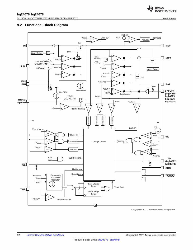
9.2 Functional Block Diagram
13
bq24076, bq24078www.ti.com SLUSCM1A –OCTOBER 2017–REVISED DECEMBER 2017
Product Folder Links: bq24076 bq24078
Submit Documentation FeedbackCopyright © 2017, Texas Instruments Incorporated
9.3 Feature Description
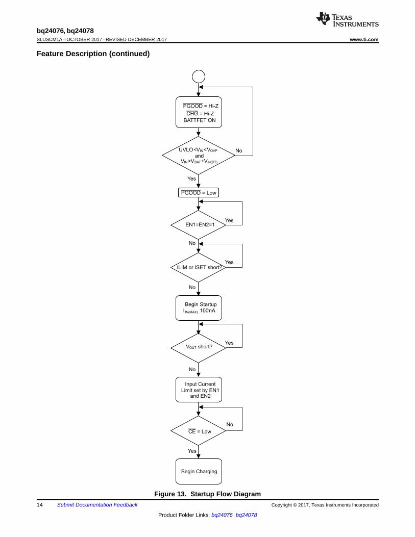
9.3.1 Undervoltage Lockout (UVLO)The bq2407x family remains in power down mode when the input voltage at the IN pin is below the undervoltagethreshold (UVLO).
During the power down mode the host commands at the control inputs (CE, EN1 and EN2) are ignored. The Q1FET connected between IN and OUT pins is off, and the status outputs CHG and PGOOD are high impedance.The Q2 FET that connects BAT to OUT is ON. (If SYSOFF is high, Q2 is off). During power down mode, theVOUT(SC2) circuitry is active and monitors for overload conditions on OUT.
9.3.2 Power OnWhen VIN exceeds the UVLO threshold, the bq2407x powers up. While VIN is below VBAT + VIN(DT), the hostcommands at the control inputs (CE, EN1 and EN2) are ignored. The Q1 FET connected between IN and OUTpins is off, and the status outputs CHG and PGOOD are high impedance. The Q2 FET that connects BAT toOUT is ON. (If SYSOFF is high, Q2 is off). During this mode, the VOUT(SC2) circuitry is active and monitors foroverload conditions on OUT.
Once VIN rises above VBAT + VIN(DT), PGOOD is driven low to indicate the valid power status and the CE, EN1,and EN2 inputs are read. The device enters standby mode if (EN1 = EN2 = HI) or if an input overvoltagecondition occurs. In standby mode, Q1 is OFF and Q2 is ON so OUT is connected to the battery input. (IfSYSOFF is high, FET Q2 is off). During this mode, the VOUT(SC2) circuitry is active and monitors for overloadconditions on OUT.
When the input voltage at IN is within the valid range: VIN > UVLO AND VIN > VBAT + VIN(DT) AND VIN < VOVP, andthe EN1 and EN2 pins indicate that the USB suspend mode is not enabled [(EN1, EN2) ≠ (HI, HI)] all internaltimers and other circuit blocks are activated. The device then checks for short-circuits at the ISET and ILIM pins.If no short conditions exists, the device switches on the input FET Q1 with a 100mA current limit to checks for ashort circuit at OUT. When VOUT is above VO(SC1), the FET Q1 switches to the current limit threshold set by EN1,EN2 and RILIM and the device enters into the normal operation. During normal operation, the system is poweredby the input source (Q1 is regulating), and the device continuously monitors the status of CE, EN1 and EN2 aswell as the input voltage conditions.
PGOOD = Low
UVLO<VIN<VOVP
andVIN>VBAT+VIN(DT)
No
Yes
EN1=EN2=1
Yes
No
ILIM or ISET short?
Yes
PGOOD = Hi-Z
CHG = Hi-Z
BATTFET ON
Begin Startup
I IN(MAX) 100mA
VOUT short?
Yes
No
No
Input Current
Limit set by EN1and EN2
CE = Low
No
Begin Charging
Yes
14
bq24076, bq24078SLUSCM1A –OCTOBER 2017–REVISED DECEMBER 2017 www.ti.com
Product Folder Links: bq24076 bq24078
Submit Documentation Feedback Copyright © 2017, Texas Instruments Incorporated
Feature Description (continued)
Figure 13. Startup Flow Diagram
50μC10μC
100 μs/div
20 m
A/d
iv
US
B1
00 C
urr
en
t L
imit
15
bq24076, bq24078www.ti.com SLUSCM1A –OCTOBER 2017–REVISED DECEMBER 2017
Product Folder Links: bq24076 bq24078
Submit Documentation FeedbackCopyright © 2017, Texas Instruments Incorporated
Feature Description (continued)9.3.3 Overvoltage Protection (OVP)The bq2407x accepts inputs up to 28 V without damage. Additionally, an overvoltage protection (OVP) circuit isimplemented that shuts off the internal LDO and discontinues charging when VIN > VOVP for a period long thantDGL(OVP). When in OVP, the system output (OUT) is connected to the battery and PGOOD is high impedance.Once the OVP condition is removed, a new power on sequence starts (see Power On). The safety timers arereset and a new charge cycle will be indicated by the CHG output.
9.3.4 Dynamic Power-Path ManagementThe bq2407x features an OUT output that powers the external load connected to the battery. This output isactive whenever a source is connected to IN or BAT. The following sections discuss the behavior of OUT with asource connected to IN to charge the battery and a battery source only.
9.3.4.1 Input Source Connected (ADAPTER or USB)With a source connected, the dynamic power-path management (DPPM) circuitry of the bq2407x monitors theinput current continuously. For the bq24076/78, OUT is regulated to 210 mV above the voltage at BAT. When theBAT voltage falls below 3.2 V, OUT is clamped to 3.41 V. This allows for proper startup of the system load evenwith a discharged battery. The current into IN is shared between charging the battery and powering the systemload at OUT. The bq2407x has internal selectable current limits of 100 mA (USB100) and 500 mA (USB500) forcharging from USB ports, as well as a resistor-programmable input current limit.
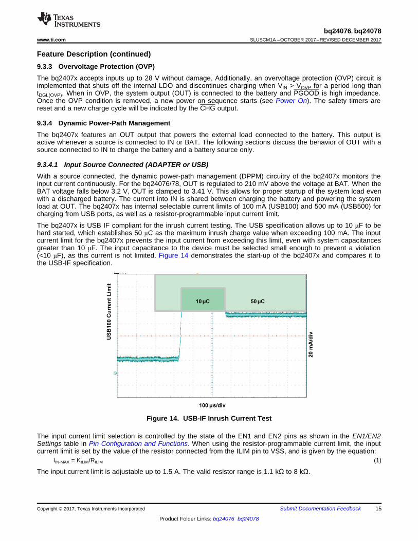
The bq2407x is USB IF compliant for the inrush current testing. The USB specification allows up to 10 μF to behard started, which establishes 50 μC as the maximum inrush charge value when exceeding 100 mA. The inputcurrent limit for the bq2407x prevents the input current from exceeding this limit, even with system capacitancesgreater than 10 μF. The input capacitance to the device must be selected small enough to prevent a violation(<10 μF), as this current is not limited. Figure 14 demonstrates the start-up of the bq2407x and compares it tothe USB-IF specification.
Figure 14. USB-IF Inrush Current Test
The input current limit selection is controlled by the state of the EN1 and EN2 pins as shown in the EN1/EN2Settings table in Pin Configuration and Functions. When using the resistor-programmable current limit, the inputcurrent limit is set by the value of the resistor connected from the ILIM pin to VSS, and is given by the equation:
IIN-MAX = KILIM/RILIM (1)
The input current limit is adjustable up to 1.5 A. The valid resistor range is 1.1 kΩ to 8 kΩ.
4 ms/div
500mV/div
USB5 Current Limit00
200mA/div
200mA/div
200mA/div
IOUT
IIN
VIN
(5V)
IBAT
Input collapses
Input current limit isreduced to preventcrashing the supply
Input regulated to VIN_DPM
16
bq24076, bq24078SLUSCM1A –OCTOBER 2017–REVISED DECEMBER 2017 www.ti.com
Product Folder Links: bq24076 bq24078
Submit Documentation Feedback Copyright © 2017, Texas Instruments Incorporated
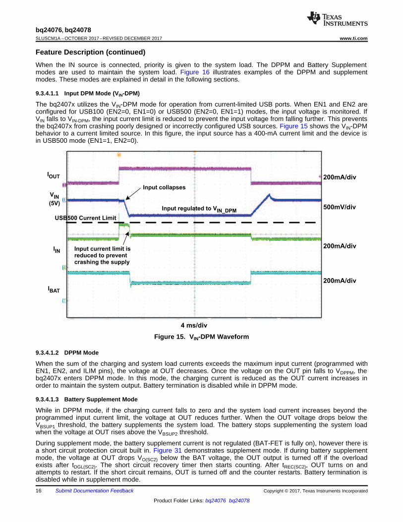
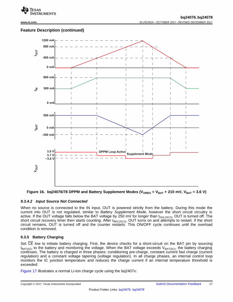
Feature Description (continued)When the IN source is connected, priority is given to the system load. The DPPM and Battery Supplementmodes are used to maintain the system load. Figure 16 illustrates examples of the DPPM and supplementmodes. These modes are explained in detail in the following sections.
9.3.4.1.1 Input DPM Mode (VIN-DPM)
The bq2407x utilizes the VIN-DPM mode for operation from current-limited USB ports. When EN1 and EN2 areconfigured for USB100 (EN2=0, EN1=0) or USB500 (EN2=0, EN1=1) modes, the input voltage is monitored. IfVIN falls to VIN-DPM, the input current limit is reduced to prevent the input voltage from falling further. This preventsthe bq2407x from crashing poorly designed or incorrectly configured USB sources. Figure 15 shows the VIN-DPMbehavior to a current limited source. In this figure, the input source has a 400-mA current limit and the device isin USB500 mode (EN1=1, EN2=0).
Figure 15. VIN-DPM Waveform
9.3.4.1.2 DPPM Mode
When the sum of the charging and system load currents exceeds the maximum input current (programmed withEN1, EN2, and ILIM pins), the voltage at OUT decreases. Once the voltage on the OUT pin falls to VDPPM, thebq2407x enters DPPM mode. In this mode, the charging current is reduced as the OUT current increases inorder to maintain the system output. Battery termination is disabled while in DPPM mode.
9.3.4.1.3 Battery Supplement Mode
While in DPPM mode, if the charging current falls to zero and the system load current increases beyond theprogrammed input current limit, the voltage at OUT reduces further. When the OUT voltage drops below theVBSUP1 threshold, the battery supplements the system load. The battery stops supplementing the system loadwhen the voltage at OUT rises above the VBSUP2 threshold.
During supplement mode, the battery supplement current is not regulated (BAT-FET is fully on), however there isa short circuit protection circuit built in. Figure 31 demonstrates supplement mode. If during battery supplementmode, the voltage at OUT drops VO(SC2) below the BAT voltage, the OUT output is turned off if the overloadexists after tDGL(SC2). The short circuit recovery timer then starts counting. After tREC(SC2), OUT turns on andattempts to restart. If the short circuit remains, OUT is turned off and the counter restarts. Battery termination isdisabled while in supplement mode.
A
1200 mA
900 mA
400 mA
0 mA
I OU
T
900 mA
500 mA
0 mA
I IN
500 mA
-300 mA
0 mA
I BA
T
3.8 V
3.7 V~3.6 V
VO
UT
DPPM Loop ActiveSupplement Mode
17
bq24076, bq24078www.ti.com SLUSCM1A –OCTOBER 2017–REVISED DECEMBER 2017
Product Folder Links: bq24076 bq24078
Submit Documentation FeedbackCopyright © 2017, Texas Instruments Incorporated
Feature Description (continued)
Figure 16. bq24076/78 DPPM and Battery Supplement Modes (VOREG = VBAT + 210 mV, VBAT = 3.6 V)
9.3.4.2 Input Source Not ConnectedWhen no source is connected to the IN input, OUT is powered strictly from the battery. During this mode thecurrent into OUT is not regulated, similar to Battery Supplement Mode, however the short circuit circuitry isactive. If the OUT voltage falls below the BAT voltage by 250 mV for longer than tDGL(SC2), OUT is turned off. Theshort circuit recovery timer then starts counting. After tREC(SC2), OUT turns on and attempts to restart. If the shortcircuit remains, OUT is turned off and the counter restarts. This ON/OFF cycle continues until the overloadcondition is removed.
9.3.5 Battery ChargingSet CE low to initiate battery charging. First, the device checks for a short-circuit on the BAT pin by sourcingIBAT(SC) to the battery and monitoring the voltage. When the BAT voltage exceeds VBAT(SC), the battery chargingcontinues. The battery is charged in three phases: conditioning pre-charge, constant current fast charge (currentregulation) and a constant voltage tapering (voltage regulation). In all charge phases, an internal control loopmonitors the IC junction temperature and reduces the charge current if an internal temperature threshold isexceeded.
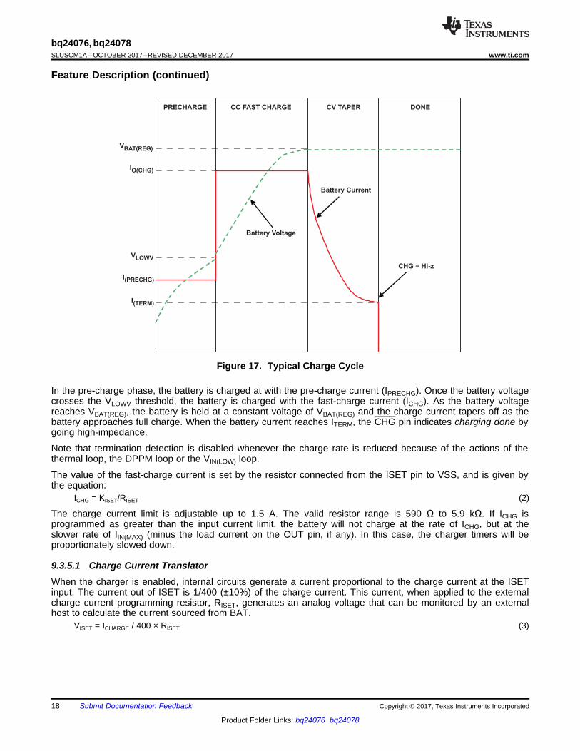
Figure 17 illustrates a normal Li-Ion charge cycle using the bq2407x:
PRECHARGE CC FAST CHARGE CV TAPER DONE
Battery Voltage
Battery Current
CHG = Hi-z
VBAT(REG)
IO(CHG)
VLOWV
I(PRECHG)
I(TERM)
18
bq24076, bq24078SLUSCM1A –OCTOBER 2017–REVISED DECEMBER 2017 www.ti.com
Product Folder Links: bq24076 bq24078
Submit Documentation Feedback Copyright © 2017, Texas Instruments Incorporated
Feature Description (continued)
Figure 17. Typical Charge Cycle
In the pre-charge phase, the battery is charged at with the pre-charge current (IPRECHG). Once the battery voltagecrosses the VLOWV threshold, the battery is charged with the fast-charge current (ICHG). As the battery voltagereaches VBAT(REG), the battery is held at a constant voltage of VBAT(REG) and the charge current tapers off as thebattery approaches full charge. When the battery current reaches ITERM, the CHG pin indicates charging done bygoing high-impedance.
Note that termination detection is disabled whenever the charge rate is reduced because of the actions of thethermal loop, the DPPM loop or the VIN(LOW) loop.
The value of the fast-charge current is set by the resistor connected from the ISET pin to VSS, and is given bythe equation:
ICHG = KISET/RISET (2)
The charge current limit is adjustable up to 1.5 A. The valid resistor range is 590 Ω to 5.9 kΩ. If ICHG isprogrammed as greater than the input current limit, the battery will not charge at the rate of ICHG, but at theslower rate of IIN(MAX) (minus the load current on the OUT pin, if any). In this case, the charger timers will beproportionately slowed down.
9.3.5.1 Charge Current TranslatorWhen the charger is enabled, internal circuits generate a current proportional to the charge current at the ISETinput. The current out of ISET is 1/400 (±10%) of the charge current. This current, when applied to the externalcharge current programming resistor, RISET, generates an analog voltage that can be monitored by an externalhost to calculate the current sourced from BAT.
VISET = ICHARGE / 400 × RISET (3)
Start Precharge
CHG = Low
Battery short detected?Yes
No
No tPRECHARGE
Elapsed?
Begin Charging
End Charge
Flash CHG
IBAT < ITERM
Yes
Yes
TD = Low(’72, ’73 Only)
( 74’ , ’75 = YES)
No
Termination Reached
BATTFET Off
Wait for VBAT < VRCH
Yes
No
VBAT > VLOWV
Start Fastcharge
ICHARGE set by ISET
No
End Charge
Flash CHG
No
tFASTCHARGE
Elapsed?
Charge Done
CHG = Hi-Z
VBAT < VRCH
No
Battery Detected?
Run Battery Detection
Yes
Yes
No
19
bq24076, bq24078www.ti.com SLUSCM1A –OCTOBER 2017–REVISED DECEMBER 2017
Product Folder Links: bq24076 bq24078
Submit Documentation FeedbackCopyright © 2017, Texas Instruments Incorporated
Feature Description (continued)
Figure 18. Battery Charging Flow Diagram
20
bq24076, bq24078SLUSCM1A –OCTOBER 2017–REVISED DECEMBER 2017 www.ti.com
Product Folder Links: bq24076 bq24078
Submit Documentation Feedback Copyright © 2017, Texas Instruments Incorporated
Feature Description (continued)9.3.5.2 Battery Detection and RechargeThe bq2407x automatically detects if a battery is connected or removed. Once a charge cycle is complete, thebattery voltage is monitored. When the battery voltage falls below VRCH, the battery detection routine is run.During battery detection, current (IBAT(DET)) is pulled from the battery for a duration tDET to see if the voltage onBAT falls below VLOWV. If not, charging begins. If it does, then it indicates that the battery is missing or theprotector is open. Next, the precharge current is applied for tDET to close the protector if possible. If VBAT < VRCH,then the protector closed and charging is initiated. If VBAT > VRCH, then the battery is determined to be missingand the detection routine continues.
9.3.5.3 Battery Disconnect (SYSOFF Input, bq24076, bq24078)The bq24076 and bq24078 feature a SYSOFF input that allows the user to turn the FET Q2 off and disconnectthe battery from the OUT pin. This is useful for disconnecting the system load from the battery, factoryprogramming where the battery is not installed or for host side impedance track fuel gauging, such as bq27500,where the battery open circuit voltage level must be detected before the battery charges or discharges. The/CHG output remains low when SYSOFF is high. Connect SYSOFF to VSS, to turn Q2 on for normal operation.SYSOFF is internally pulled to VBAT through ~5 MΩ resistor.
9.3.5.4 Dynamic Charge Timers (TMR Input)The bq2407x devices contain internal safety timers for the pre-charge and fast-charge phases to preventpotential damage to the battery and the system. The timers begin at the start of the respective charge cycles.The timer values are programmed by connecting a resistor from TMR to VSS. The resistor value is calculatedusing the following equation:
tPRECHG = KTMR × RTMR (4)tMAXCHG = 10 × KTMR × RTMR (5)
Leave TMR unconnected to select the internal default timers. Disable the timers by connecting TMR to VSS.
Reset the timers by toggling the CE pin, or by toggling EN1, EN2 pin to put the device in and out of USBsuspend mode (EN1 = HI, EN2 = HI).
Note that timers are suspended when the device is in thermal shutdown, and the timers are slowed proportionallyto the charge current when the device enters thermal regulation.
During the fast charge phase, several events increase the timer durations.• The system load current activates the DPPM loop which reduces the available charging current• The input current is reduced because the input voltage has fallen to VIN(LOW)• The device has entered thermal regulation because the IC junction temperature has exceeded TJ(REG)
During each of these events, the internal timers are slowed down proportionately to the reduction in chargingcurrent. For example, if the charging current is reduced by half for two minutes, the timer clock is reduced to halfthe frequency and the counter counts half as fast resulting in only one minute of "counting" time.
If the pre charge timer expires before the battery voltage reaches VLOWV, the bq2407x indicates a fault condition.Additionally, if the battery current does not fall to ITERM before the fast charge timer expires, a fault is indicated.The CHG output flashes at approximately 2 Hz to indicate a fault condition. The fault condition is cleared bytoggling CE or the input power, entering/ exiting USB suspend mode, or an OVP event.
9.3.5.5 Status Indicators (PGOOD, CHG)The bq2407x contains two open-drain outputs that signal its status. The PGOOD output signals when a validinput source is connected. PGOOD is low when (VBAT + VIN(DT)) < VIN < VOVP. When the input voltage is outsideof this range, PGOOD is high impedance.
The charge cycle after power-up, CE going low, or exiting OVP is indicated with the CHG pin on (low - LED on),whereas all refresh (subsequent) charges will result in the CHG pin off (open - LED off). In addition, the CHGsignals timer faults by flashing at approximately 2 Hz.
21
bq24076, bq24078www.ti.com SLUSCM1A –OCTOBER 2017–REVISED DECEMBER 2017
Product Folder Links: bq24076 bq24078
Submit Documentation FeedbackCopyright © 2017, Texas Instruments Incorporated
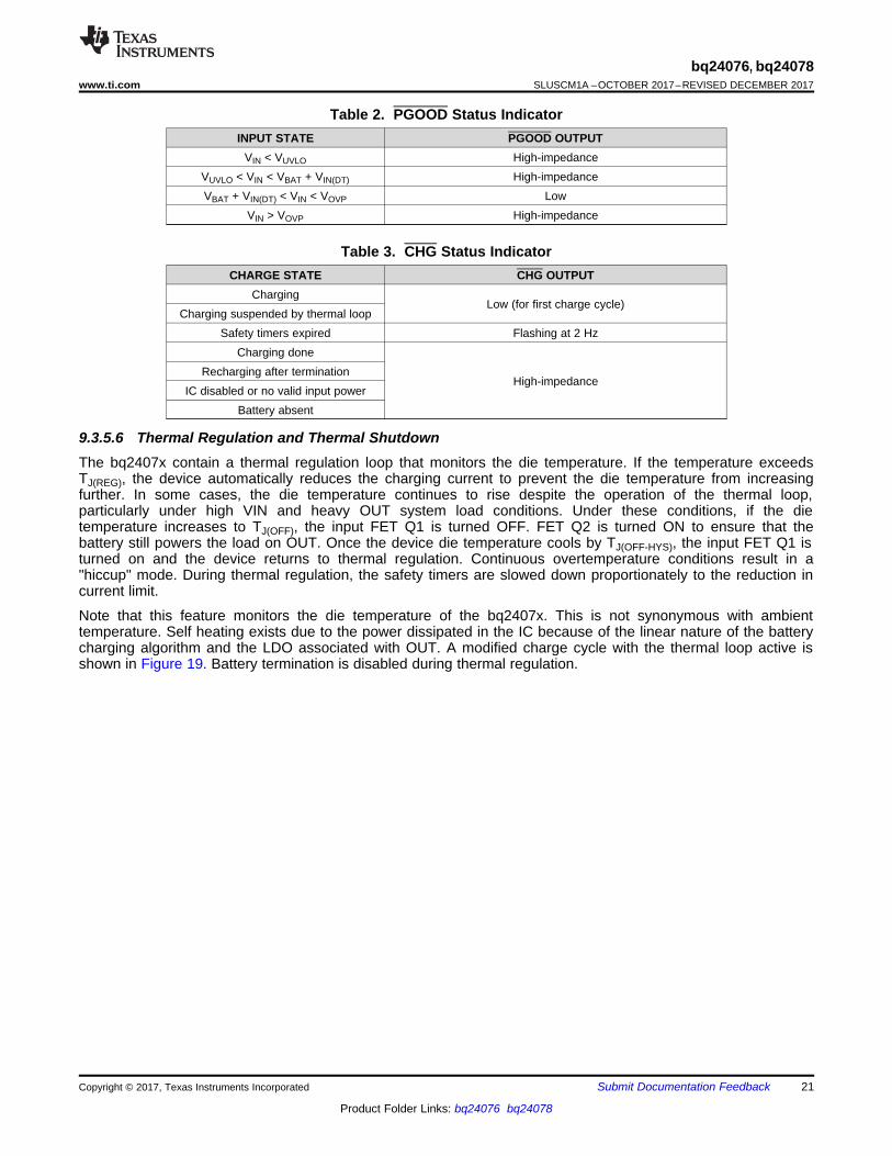
Table 2. PGOOD Status IndicatorINPUT STATE PGOOD OUTPUT
VIN < VUVLO High-impedanceVUVLO < VIN < VBAT + VIN(DT) High-impedanceVBAT + VIN(DT) < VIN < VOVP Low
VIN > VOVP High-impedance
Table 3. CHG Status IndicatorCHARGE STATE CHG OUTPUT
ChargingLow (for first charge cycle)
Charging suspended by thermal loopSafety timers expired Flashing at 2 Hz
Charging done
High-impedanceRecharging after termination
IC disabled or no valid input powerBattery absent
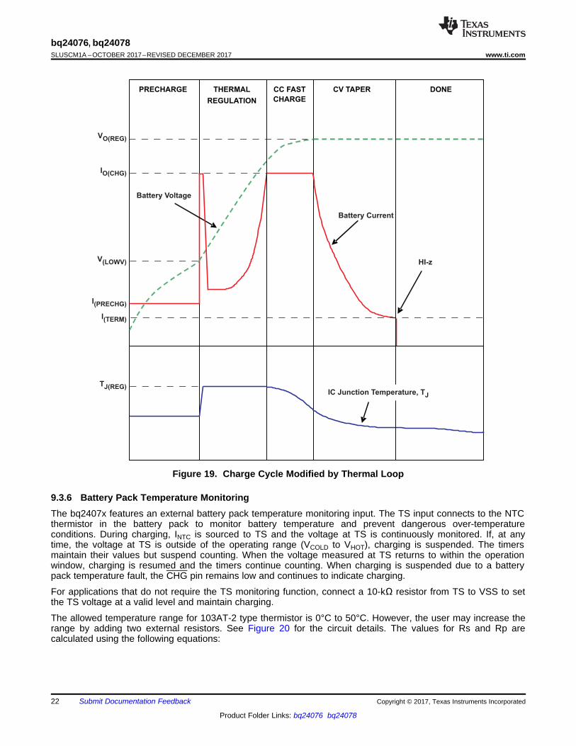
9.3.5.6 Thermal Regulation and Thermal ShutdownThe bq2407x contain a thermal regulation loop that monitors the die temperature. If the temperature exceedsTJ(REG), the device automatically reduces the charging current to prevent the die temperature from increasingfurther. In some cases, the die temperature continues to rise despite the operation of the thermal loop,particularly under high VIN and heavy OUT system load conditions. Under these conditions, if the dietemperature increases to TJ(OFF), the input FET Q1 is turned OFF. FET Q2 is turned ON to ensure that thebattery still powers the load on OUT. Once the device die temperature cools by TJ(OFF-HYS), the input FET Q1 isturned on and the device returns to thermal regulation. Continuous overtemperature conditions result in a"hiccup" mode. During thermal regulation, the safety timers are slowed down proportionately to the reduction incurrent limit.
Note that this feature monitors the die temperature of the bq2407x. This is not synonymous with ambienttemperature. Self heating exists due to the power dissipated in the IC because of the linear nature of the batterycharging algorithm and the LDO associated with OUT. A modified charge cycle with the thermal loop active isshown in Figure 19. Battery termination is disabled during thermal regulation.
PRECHARGE CC FAST
CHARGE
CV TAPER DONETHERMAL
REGULATION
Battery Voltage
Battery Current
HI-z
IC Junction Temperature, TJ
VO(REG)
IO(CHG)
V(LOWV)
I(PRECHG)
I(TERM)
TJ(REG)
22
bq24076, bq24078SLUSCM1A –OCTOBER 2017–REVISED DECEMBER 2017 www.ti.com
Product Folder Links: bq24076 bq24078
Submit Documentation Feedback Copyright © 2017, Texas Instruments Incorporated
Figure 19. Charge Cycle Modified by Thermal Loop
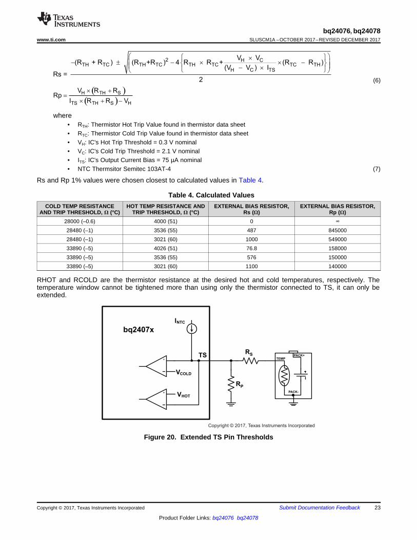
9.3.6 Battery Pack Temperature MonitoringThe bq2407x features an external battery pack temperature monitoring input. The TS input connects to the NTCthermistor in the battery pack to monitor battery temperature and prevent dangerous over-temperatureconditions. During charging, INTC is sourced to TS and the voltage at TS is continuously monitored. If, at anytime, the voltage at TS is outside of the operating range (VCOLD to VHOT), charging is suspended. The timersmaintain their values but suspend counting. When the voltage measured at TS returns to within the operationwindow, charging is resumed and the timers continue counting. When charging is suspended due to a batterypack temperature fault, the CHG pin remains low and continues to indicate charging.
For applications that do not require the TS monitoring function, connect a 10-kΩ resistor from TS to VSS to setthe TS voltage at a valid level and maintain charging.
The allowed temperature range for 103AT-2 type thermistor is 0°C to 50°C. However, the user may increase therange by adding two external resistors. See Figure 20 for the circuit details. The values for Rs and Rp arecalculated using the following equations:
bq2407x
TSTEMP
PACK+
PACK-
+
+ VHOT
VCOLD
INTC
RP
RS
Copyright © 2017, Texas Instruments Incorporated
( )( )
H TH S
TS TH S H
V R RRp
I R R V
´ +=
´ + -
2 H CTH TC TH TC TH TC TC TH
H C TS
V V(R + R ) (R +R ) 4 R R + (R R )
(V V ) IRs =
2
æ öì ü´- ± - ´ ´ -ç ÷í ýç ÷- ´î þè ø
23
bq24076, bq24078www.ti.com SLUSCM1A –OCTOBER 2017–REVISED DECEMBER 2017
Product Folder Links: bq24076 bq24078
Submit Documentation FeedbackCopyright © 2017, Texas Instruments Incorporated
(6)
where• RTH: Thermistor Hot Trip Value found in thermistor data sheet• RTC: Thermistor Cold Trip Value found in thermistor data sheet• VH: IC's Hot Trip Threshold = 0.3 V nominal• VC: IC's Cold Trip Threshold = 2.1 V nominal• ITS: IC's Output Current Bias = 75 µA nominal• NTC Thermsitor Semitec 103AT-4 (7)
Rs and Rp 1% values were chosen closest to calculated values in Table 4.
Table 4. Calculated ValuesCOLD TEMP RESISTANCE
AND TRIP THRESHOLD, Ω (°C)HOT TEMP RESISTANCE AND
TRIP THRESHOLD, Ω (°C)EXTERNAL BIAS RESISTOR,
Rs (Ω)EXTERNAL BIAS RESISTOR,
Rp (Ω)28000 (–0.6) 4000 (51) 0 ∞28480 (–1) 3536 (55) 487 84500028480 (–1) 3021 (60) 1000 54900033890 (–5) 4026 (51) 76.8 15800033890 (–5) 3536 (55) 576 15000033890 (–5) 3021 (60) 1100 140000
RHOT and RCOLD are the thermistor resistance at the desired hot and cold temperatures, respectively. Thetemperature window cannot be tightened more than using only the thermistor connected to TS, it can only beextended.
Figure 20. Extended TS Pin Thresholds
VBAT
VLOWV
ICHG
IPRE-CHGPre-Charge
Fast-Charge
Pre-Charge
Fast-Charge
t < tDGL1(LOWV) tDGL1(LOWV)tDGL2(LOWV) t < tDGL2(LOWV)
tDGL1(LOWV)
VOVP
V - VOVP hys(OVP)
V + VBAT IN(DT)
V + V - VBAT IN(DT) hys(INDT)
UVLO
UVLO - Vhys(UVLO)
PGOOD
tDGL(PGOOD)
tDGL(OVP)
tDGL(PGOOD)
tDGL(NO-IN)
VIN
t < tDGL(OVP)
Typical Input VoltageOperating Range
24
bq24076, bq24078SLUSCM1A –OCTOBER 2017–REVISED DECEMBER 2017 www.ti.com
Product Folder Links: bq24076 bq24078
Submit Documentation Feedback Copyright © 2017, Texas Instruments Incorporated
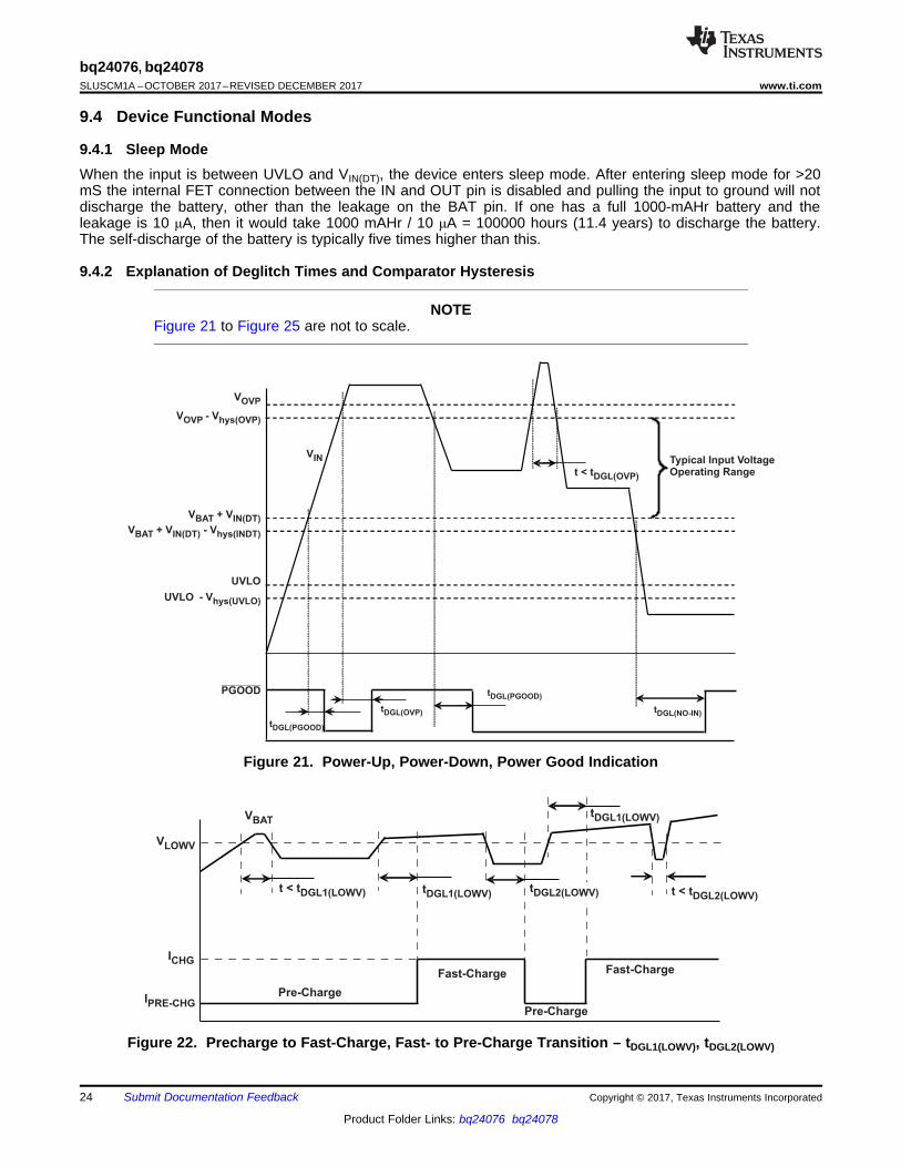
9.4 Device Functional Modes
9.4.1 Sleep ModeWhen the input is between UVLO and VIN(DT), the device enters sleep mode. After entering sleep mode for >20mS the internal FET connection between the IN and OUT pin is disabled and pulling the input to ground will notdischarge the battery, other than the leakage on the BAT pin. If one has a full 1000-mAHr battery and theleakage is 10 μA, then it would take 1000 mAHr / 10 μA = 100000 hours (11.4 years) to discharge the battery.The self-discharge of the battery is typically five times higher than this.
9.4.2 Explanation of Deglitch Times and Comparator Hysteresis
NOTEFigure 21 to Figure 25 are not to scale.
Figure 21. Power-Up, Power-Down, Power Good Indication
Figure 22. Precharge to Fast-Charge, Fast- to Pre-Charge Transition – tDGL1(LOWV), tDGL2(LOWV)
VCOLD
V - VCOLD hys(COLD)
V - VHOT hys(HOT)
VHOT
VTS
t < tDGL(TS) tDGL(TS)
SuspendCharging
ResumeCharging
TurnQ2 OFF
tREC(SC2)
ForceQ2 ON
TurnQ2 OFF
tREC(SC2)
ForceQ2 ON
V - VBAT OUT
VO(SC2)
Recover
t < tDGL(SC2)tDGL(SC2) tDGL(SC2) t < tDGL(SC2)
VRCH
VBAT
t < tDGL(RCH) tDGL(RCH)
Re-Charge
25
bq24076, bq24078www.ti.com SLUSCM1A –OCTOBER 2017–REVISED DECEMBER 2017
Product Folder Links: bq24076 bq24078
Submit Documentation FeedbackCopyright © 2017, Texas Instruments Incorporated
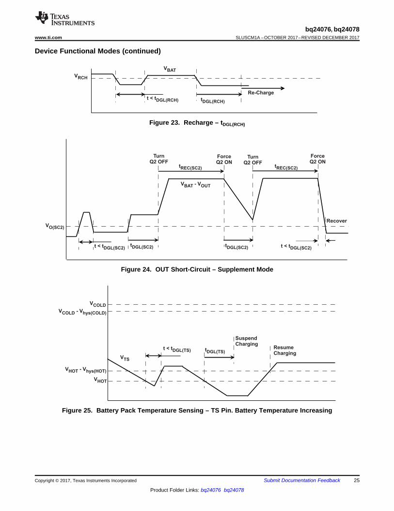
Device Functional Modes (continued)
Figure 23. Recharge – tDGL(RCH)
Figure 24. OUT Short-Circuit – Supplement Mode
Figure 25. Battery Pack Temperature Sensing – TS Pin. Battery Temperature Increasing
IN
VSS
BAT
ISE
T
DC+
GND
Adaptor
HOSTbq24076bq24078
CE
PG
OO
D
OUT
SYSOFF
EN1
EN2
TS
TEMPPACK+
PACK- R3
1.13 kW
R4
1.5 kW
R1
46.4 kW
SYSTEM
CH
G
TM
R
ILM
R2
1.18 kW
R5
1.5 kW
C2
4.7 FmC1
1 Fm
C3
4.7 Fm
Copyright © 2017, Texas Instruments Incorporated
26
bq24076, bq24078SLUSCM1A –OCTOBER 2017–REVISED DECEMBER 2017 www.ti.com
Product Folder Links: bq24076 bq24078
Submit Documentation Feedback Copyright © 2017, Texas Instruments Incorporated
10 Application and Implementation
NOTEInformation in the following applications sections is not part of the TI componentspecification, and TI does not warrant its accuracy or completeness. TI’s customers areresponsible for determining suitability of components for their purposes. Customers shouldvalidate and test their design implementation to confirm system functionality.
10.1 Application InformationThe bq2407x devices power the system while simultaneously and independently charging the battery. The inputpower source for charging the battery and running the system can be an AC adapter or a USB port. The devicesfeature dynamic power-path management (DPPM), which shares the source current between the system andbattery charging and automatically reduces the charging current if the system load increases. When chargingfrom a USB port, the input dynamic power management (VIN-DPM) circuit reduces the input current limit if theinput voltage falls below a threshold, preventing the USB port from crashing. The power-path architecture alsopermits the battery to supplement the system current requirements when the adapter cannot deliver the peaksystem currents.
The bq2407x is configurable to be host controlled for selecting different input current limits based on the inputsource connected, or a fully stand alone device for applications that do not support multiple types of inputsources.
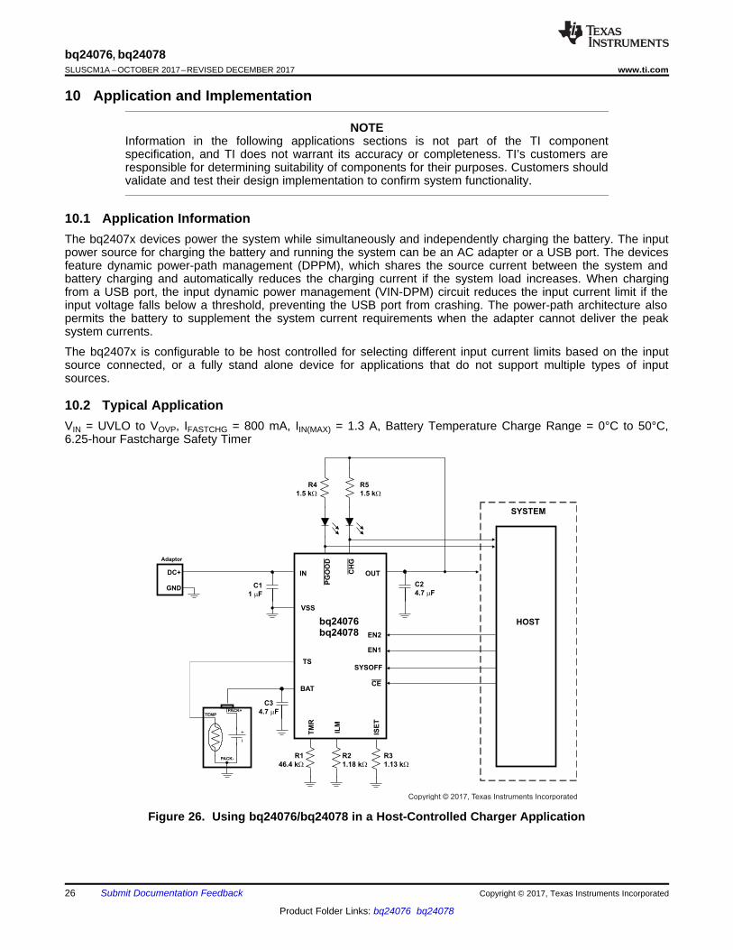
10.2 Typical ApplicationVIN = UVLO to VOVP, IFASTCHG = 800 mA, IIN(MAX) = 1.3 A, Battery Temperature Charge Range = 0°C to 50°C,6.25-hour Fastcharge Safety Timer
Figure 26. Using bq24076/bq24078 in a Host-Controlled Charger Application
27
bq24076, bq24078www.ti.com SLUSCM1A –OCTOBER 2017–REVISED DECEMBER 2017
Product Folder Links: bq24076 bq24078
Submit Documentation FeedbackCopyright © 2017, Texas Instruments Incorporated
Typical Application (continued)10.2.1 Design Requirements• Supply voltage = 5 V• Fast charge current of approximately 800 mA; ISET - pin 16• Input current limit = 1.3 A; ILIM - pin 12• Termination current threshold = 110 mA; ITERM – pin 15 (bq24074 only)• Safety timer duration, Fast-Charge = 6.25 hours; TMR – pin 14• TS – Battery Temperature Sense = 10 kΩ NTC (103AT-2)
10.2.2 Detailed Design Procedure
10.2.2.1 bq2407x Charger Design ExampleSee Figure 26 for a schematic of the design example.
10.2.2.1.1 System ON/OFF (SYSOFF) (bq24076 or bq24078 only)
Connect SYSOFF high to disconnect the battery from the system load. Connect SYSOFF low for normaloperation
10.2.2.2 Calculations
10.2.2.2.1 Program the Fast Charge Current (ISET):
RISET = KISET / ICHGKISET = 890 AΩ from the electrical characteristics table.RISET = 890 AΩ / 0.8 A = 1.1125 kΩ
Select the closest standard value, which for this case is 1.13 kΩ. Connect this resistor between ISET (pin 16)and VSS.
10.2.2.2.2 Program the Input Current Limit (ILIM)
RILIM = KILIM / II_MAXKILIM = 1550 AΩ from the electrical characteristics table.RISET = 1550 AΩ / 1.3 A = 1.192 kΩ
Select the closest standard value, which for this case is 1.18 kΩ. Connect this resistor between ILIM (pin 12) andVSS.
10.2.2.2.3 Program 6.25-hour Fast-Charge Safety Timer (TMR)
RTMR = tMAXCHG / (10 × KTMR )KTMR = 48 s/kΩ from the electrical characteristics table.RTMR = (6.25 hr × 3600 s/hr) / (10 × 48 s/kΩ) = 46.8 kΩ
Select the closest standard value, which for this case is 46.4 kΩ. Connect this resistor between TMR (pin 2) andVSS.
10.2.2.3 TS FunctionUse a 10-kΩ NTC thermistor in the battery pack (103AT-2). For applications that do not require the TSmonitoring function, connect a 10-kΩ resistor from TS to VSS to set the TS voltage at a valid level and maintaincharging.
10.2.2.4 CHG and PGOODLED Status: Connect a 1.5-kΩ resistor in series with a LED between OUT and CHG to indicate charging status.Connect a 1.5-kΩ resistor in series with a LED between OUT and PGOOD to indicate when a valid input sourceis connected.
28
bq24076, bq24078SLUSCM1A –OCTOBER 2017–REVISED DECEMBER 2017 www.ti.com
Product Folder Links: bq24076 bq24078
Submit Documentation Feedback Copyright © 2017, Texas Instruments Incorporated
Typical Application (continued)Processor Monitoring Status: Connect a pullup resistor (on the order of 100 kΩ) between the power rail of theprocessor and CHG and PGOOD.
10.2.2.5 Selecting IN, OUT, and BAT Pin CapacitorsIn most applications, all that is needed is a high-frequency decoupling capacitor (ceramic) on the power pin,input, output and battery pins. Using the values shown on the application diagram, is recommended. Afterevaluation of these voltage signals with real system operational conditions, one can determine if capacitancevalues can be adjusted toward the minimum recommended values (DC load application) or higher values for fasthigh amplitude pulsed load applications. Note if designed high input voltage sources (bad adaptors or wrongadaptors), the capacitor needs to be rated appropriately. Ceramic capacitors are tested to 2x their rated valuesso a 16-V capacitor may be adequate for a 30-V transient (verify tested rating with capacitor manufacturer).
IOUT
IBAT
V
3.8 VBAT
500 mA/div
500 mV/div
1 ms/div
V
4.4 VOUT
1 A/div
Supplement Mode
IOUT
IBAT
V
3.6 VBAT
500 mA/div
200 mV/div
1 ms/div
V
3.81 VOUT
1 A/div
Supplement Mode
Tracking to V +210 mVBAT
VCHG
IBAT
2 V/div
400 ms/div
VBAT
1 A/div
5 V/div
BatteryRemoved
Battery Detection Mode
IOUT
IBAT
200 mV/div
400 s/divm
V
4.4 V
OUT
500 mA/div
500 mA/div
VCHG
IBAT
2 V/div
400 ms/div
VBAT
1 A/div
5 V/div
Charging Initiated
Battery Detection Mode
Battery Inserted
VIN
500 mV/div
4 ms/div
5 V/div
IBAT
VPGOOD 5 V/div
V
4.4 V
OUT
V
3.6 V
BAT
500 mA/div
29
bq24076, bq24078www.ti.com SLUSCM1A –OCTOBER 2017–REVISED DECEMBER 2017
Product Folder Links: bq24076 bq24078
Submit Documentation FeedbackCopyright © 2017, Texas Instruments Incorporated
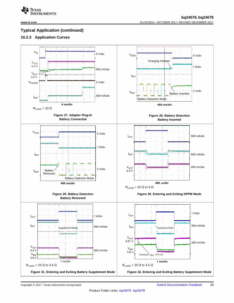
Typical Application (continued)10.2.3 Application Curves
RLOAD = 10 Ω
Figure 27. Adapter Plug-InBattery Connected
Figure 28. Battery DetectionBattery Inserted
Figure 29. Battery DetectionBattery Removed
RLOAD = 20 Ω to 9 Ω
Figure 30. Entering and Exiting DPPM Mode
RLOAD = 25 Ω to 4.5 Ω
Figure 31. Entering and Exiting Battery Supplement Mode
RLOAD = 20 Ω to 4.5 Ω
Figure 32. Entering and Exiting Battery Supplement Mode
5 V/div
2 V/div
400 s/divm
500 mA/div
VSYSOFF
IBAT
V
4 V
BAT
V
5.5 V
OUT
5 V/div
500 mA/div
4 ms/div
2 V/div
VSYSOFF
IBAT
V
4 VBAT
VOUT
Battery PoweringSystem System Power Off
10 V/div
500 mV/div
1 A/div
40 s/divm
VIN
IBAT
V
4.2 V
BAT
V
4.4 V
OUT
VCE
IBAT
V
3.6 VBAT
VCHG
500 mA/div
1 V/div
5 V/div
5 V/div
10 ms/div
Mandatory Precharge
30
bq24076, bq24078SLUSCM1A –OCTOBER 2017–REVISED DECEMBER 2017 www.ti.com
Product Folder Links: bq24076 bq24078
Submit Documentation Feedback Copyright © 2017, Texas Instruments Incorporated
Typical Application (continued)
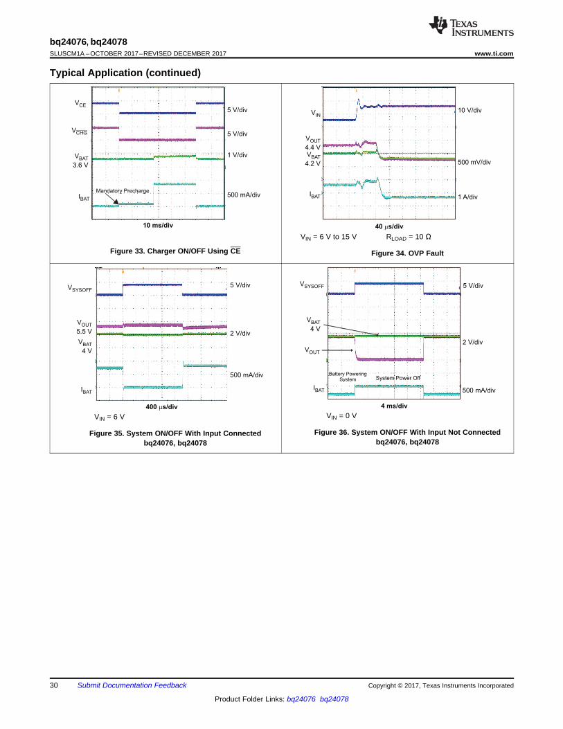
Figure 33. Charger ON/OFF Using CE
VIN = 6 V to 15 V RLOAD = 10 Ω
Figure 34. OVP Fault
VIN = 6 V
Figure 35. System ON/OFF With Input Connectedbq24076, bq24078
VIN = 0 V
Figure 36. System ON/OFF With Input Not Connectedbq24076, bq24078
31
bq24076, bq24078www.ti.com SLUSCM1A –OCTOBER 2017–REVISED DECEMBER 2017
Product Folder Links: bq24076 bq24078
Submit Documentation FeedbackCopyright © 2017, Texas Instruments Incorporated
11 Power Supply RecommendationsSome adapters implement a half rectifier topology, which causes the adapter output voltage to fall below thebattery voltage during part of the cycle. To enable operation with adapters under those conditions, the bq2407xfamily keeps the charger on for at least 20 msec (typical) after the input power puts the part in sleep mode. Thisfeature enables use of external adapters using 50 Hz networks. The input must not drop below the UVLO voltagefor the charger to work properly. Thus, the battery voltage should be above the UVLO to help prevent the inputfrom dropping out. Additional input capacitance may be needed.
12 Layout
12.1 Layout Guidelines• To obtain optimal performance, the decoupling capacitor from IN to GND (thermal pad) and the output filter
capacitors from OUT to GND (thermal pad) should be placed as close as possible to the bq2407x, with shorttrace runs to both IN, OUT and GND (thermal pad).
• All low-current GND connections should be kept separate from the high-current charge or discharge pathsfrom the battery. Use a single-point ground technique incorporating both the small signal ground path and thepower ground path.
• The high current charge paths into IN pin and from the OUT pin must be sized appropriately for the maximumcharge current in order to avoid voltage drops in these traces
• The bq2407x family is packaged in a thermally enhanced MLP package. The package includes a thermal padto provide an effective thermal contact between the IC and the printed circuit board (PCB); this thermal pad isalso the main ground connection for the device. Connect the thermal pad to the PCB ground connection. FullPCB design guidelines for this package are provided in QFN/SON PCB Attachment Application Note(SLUA271).
32
bq24076, bq24078SLUSCM1A –OCTOBER 2017–REVISED DECEMBER 2017 www.ti.com
Product Folder Links: bq24076 bq24078
Submit Documentation Feedback Copyright © 2017, Texas Instruments Incorporated
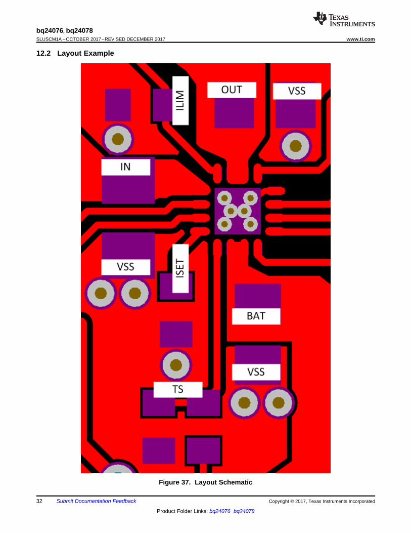
12.2 Layout Example
Figure 37. Layout Schematic
33
bq24076, bq24078www.ti.com SLUSCM1A –OCTOBER 2017–REVISED DECEMBER 2017
Product Folder Links: bq24076 bq24078
Submit Documentation FeedbackCopyright © 2017, Texas Instruments Incorporated
12.3 Thermal ConsiderationsThe bq24076/78 family is packaged in a thermally enhanced MLP package. The package includes a thermal padto provide an effective thermal contact between the IC and the printed circuit board (PCB). The power padshould be directly connected to the VSS pin. Full PCB design guidelines for this package are provided inQFN/SON PCB Attachment Application Note (SLUA271). The most common measure of package thermalperformance is thermal impedance (θJA ) measured (or modeled) from the chip junction to the air surrounding thepackage surface (ambient). The mathematical expression for θJA is:
θJA = (TJ - T) / P
where• TJ = chip junction temperature• T = ambient temperature• P = device power dissipation (8)
Factors that can influence the measurement and calculation of θJA include:
• Whether or not the device is board mounted• Trace size, composition, thickness, and geometry• Orientation of the device (horizontal or vertical)• Volume of the ambient air surrounding the device under test and airflow• Whether other surfaces are in close proximity to the device being tested
Due to the charge profile of Li-Ion batteries the maximum power dissipation is typically seen at the beginning ofthe charge cycle when the battery voltage is at its lowest. Typically after fast charge begins the pack voltageincreases to ≉3.4 V within the first 2 minutes. The thermal time constant of the assembly typically takes a fewminutes to heat up so when doing maximum power dissipation calculations, 3.4 V is a good minimum voltage touse. This is verified, with the system and a fully discharged battery, by plotting temperature on the bottom of thePCB under the IC (pad should have multiple vias), the charge current and the battery voltage as a function oftime. The fast charge current will start to taper off if the part goes into thermal regulation.
The device power dissipation, P, is a function of the charge rate and the voltage drop across the internalPowerFET. It can be calculated from the following equation when a battery pack is being charged :
P = [V(IN) – V(OUT)] × I(OUT) + [V(OUT) – V(BAT)] × I(BAT) (9)
The thermal loop feature reduces the charge current to limit excessive IC junction temperature. It isrecommended that the design not run in thermal regulation for typical operating conditions (nominal input voltageand nominal ambient temperatures) and use the feature for non typical situations such as hot environments orhigher than normal input source voltage. With that said, the IC will still perform as described, if the thermal loopis always active.
34
bq24076, bq24078SLUSCM1A –OCTOBER 2017–REVISED DECEMBER 2017 www.ti.com
Product Folder Links: bq24076 bq24078
Submit Documentation Feedback Copyright © 2017, Texas Instruments Incorporated
13 Device and Documentation Support
13.1 Device Support
13.1.1 Third-Party Products DisclaimerTI'S PUBLICATION OF INFORMATION REGARDING THIRD-PARTY PRODUCTS OR SERVICES DOES NOTCONSTITUTE AN ENDORSEMENT REGARDING THE SUITABILITY OF SUCH PRODUCTS OR SERVICESOR A WARRANTY, REPRESENTATION OR ENDORSEMENT OF SUCH PRODUCTS OR SERVICES, EITHERALONE OR IN COMBINATION WITH ANY TI PRODUCT OR SERVICE.
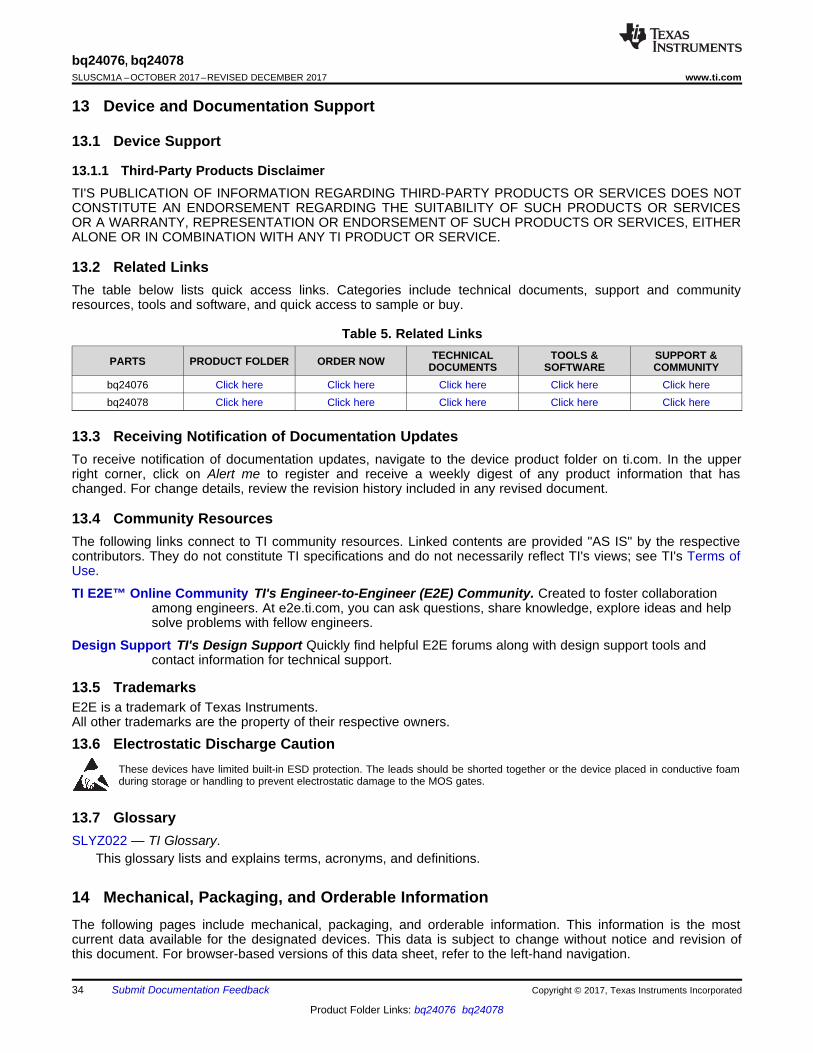
13.2 Related LinksThe table below lists quick access links. Categories include technical documents, support and communityresources, tools and software, and quick access to sample or buy.
Table 5. Related Links
PARTS PRODUCT FOLDER ORDER NOW TECHNICALDOCUMENTS
TOOLS &SOFTWARE
SUPPORT &COMMUNITY
bq24076 Click here Click here Click here Click here Click herebq24078 Click here Click here Click here Click here Click here
13.3 Receiving Notification of Documentation UpdatesTo receive notification of documentation updates, navigate to the device product folder on ti.com. In the upperright corner, click on Alert me to register and receive a weekly digest of any product information that haschanged. For change details, review the revision history included in any revised document.
13.4 Community ResourcesThe following links connect to TI community resources. Linked contents are provided "AS IS" by the respectivecontributors. They do not constitute TI specifications and do not necessarily reflect TI's views; see TI's Terms ofUse.
TI E2E™ Online Community TI's Engineer-to-Engineer (E2E) Community. Created to foster collaborationamong engineers. At e2e.ti.com, you can ask questions, share knowledge, explore ideas and helpsolve problems with fellow engineers.
Design Support TI's Design Support Quickly find helpful E2E forums along with design support tools andcontact information for technical support.
13.5 TrademarksE2E is a trademark of Texas Instruments.All other trademarks are the property of their respective owners.
13.6 Electrostatic Discharge CautionThese devices have limited built-in ESD protection. The leads should be shorted together or the device placed in conductive foamduring storage or handling to prevent electrostatic damage to the MOS gates.
13.7 GlossarySLYZ022 — TI Glossary.
This glossary lists and explains terms, acronyms, and definitions.
14 Mechanical, Packaging, and Orderable InformationThe following pages include mechanical, packaging, and orderable information. This information is the mostcurrent data available for the designated devices. This data is subject to change without notice and revision ofthis document. For browser-based versions of this data sheet, refer to the left-hand navigation.
PACKAGE OPTION ADDENDUM
www.ti.com 4-Dec-2017
Addendum-Page 1
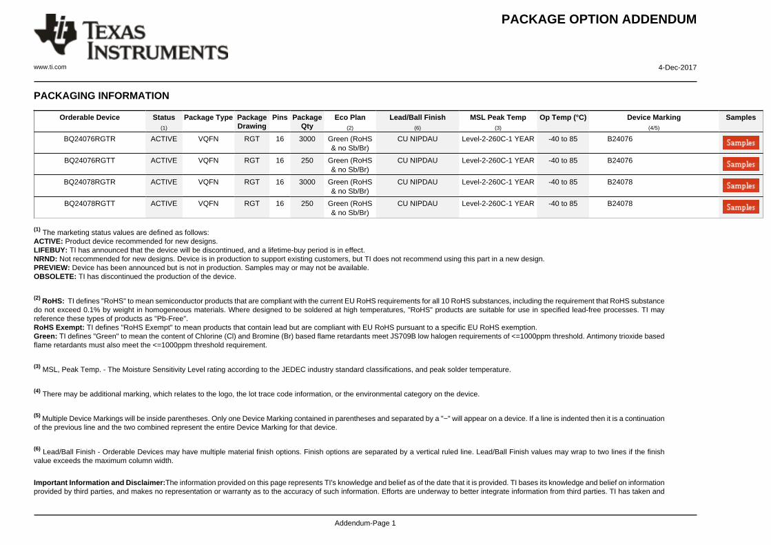
PACKAGING INFORMATION
Orderable Device Status(1)
Package Type PackageDrawing
Pins PackageQty
Eco Plan(2)
Lead/Ball Finish(6)
MSL Peak Temp(3)
Op Temp (°C) Device Marking(4/5)
Samples
BQ24076RGTR ACTIVE VQFN RGT 16 3000 Green (RoHS& no Sb/Br)
CU NIPDAU Level-2-260C-1 YEAR -40 to 85 B24076
BQ24076RGTT ACTIVE VQFN RGT 16 250 Green (RoHS& no Sb/Br)
CU NIPDAU Level-2-260C-1 YEAR -40 to 85 B24076
BQ24078RGTR ACTIVE VQFN RGT 16 3000 Green (RoHS& no Sb/Br)
CU NIPDAU Level-2-260C-1 YEAR -40 to 85 B24078
BQ24078RGTT ACTIVE VQFN RGT 16 250 Green (RoHS& no Sb/Br)
CU NIPDAU Level-2-260C-1 YEAR -40 to 85 B24078
(1) The marketing status values are defined as follows:ACTIVE: Product device recommended for new designs.LIFEBUY: TI has announced that the device will be discontinued, and a lifetime-buy period is in effect.NRND: Not recommended for new designs. Device is in production to support existing customers, but TI does not recommend using this part in a new design.PREVIEW: Device has been announced but is not in production. Samples may or may not be available.OBSOLETE: TI has discontinued the production of the device.
(2) RoHS: TI defines "RoHS" to mean semiconductor products that are compliant with the current EU RoHS requirements for all 10 RoHS substances, including the requirement that RoHS substancedo not exceed 0.1% by weight in homogeneous materials. Where designed to be soldered at high temperatures, "RoHS" products are suitable for use in specified lead-free processes. TI mayreference these types of products as "Pb-Free".RoHS Exempt: TI defines "RoHS Exempt" to mean products that contain lead but are compliant with EU RoHS pursuant to a specific EU RoHS exemption.Green: TI defines "Green" to mean the content of Chlorine (Cl) and Bromine (Br) based flame retardants meet JS709B low halogen requirements of <=1000ppm threshold. Antimony trioxide basedflame retardants must also meet the <=1000ppm threshold requirement.
(3) MSL, Peak Temp. - The Moisture Sensitivity Level rating according to the JEDEC industry standard classifications, and peak solder temperature.
(4) There may be additional marking, which relates to the logo, the lot trace code information, or the environmental category on the device.
(5) Multiple Device Markings will be inside parentheses. Only one Device Marking contained in parentheses and separated by a "~" will appear on a device. If a line is indented then it is a continuationof the previous line and the two combined represent the entire Device Marking for that device.
(6) Lead/Ball Finish - Orderable Devices may have multiple material finish options. Finish options are separated by a vertical ruled line. Lead/Ball Finish values may wrap to two lines if the finishvalue exceeds the maximum column width.
Important Information and Disclaimer:The information provided on this page represents TI's knowledge and belief as of the date that it is provided. TI bases its knowledge and belief on informationprovided by third parties, and makes no representation or warranty as to the accuracy of such information. Efforts are underway to better integrate information from third parties. TI has taken and
PACKAGE OPTION ADDENDUM
www.ti.com 4-Dec-2017
Addendum-Page 2
continues to take reasonable steps to provide representative and accurate information but may not have conducted destructive testing or chemical analysis on incoming materials and chemicals.TI and TI suppliers consider certain information to be proprietary, and thus CAS numbers and other limited information may not be available for release.
In no event shall TI's liability arising out of such information exceed the total purchase price of the TI part(s) at issue in this document sold by TI to Customer on an annual basis.
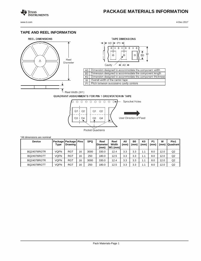
TAPE AND REEL INFORMATION
*All dimensions are nominal
Device PackageType
PackageDrawing
Pins SPQ ReelDiameter
(mm)
ReelWidth
W1 (mm)
A0(mm)
B0(mm)
K0(mm)
P1(mm)
W(mm)
Pin1Quadrant
BQ24076RGTR VQFN RGT 16 3000 330.0 12.4 3.3 3.3 1.1 8.0 12.0 Q2
BQ24076RGTT VQFN RGT 16 250 180.0 12.5 3.3 3.3 1.1 8.0 12.0 Q2
BQ24078RGTR VQFN RGT 16 3000 330.0 12.4 3.3 3.3 1.1 8.0 12.0 Q2
BQ24078RGTT VQFN RGT 16 250 180.0 12.5 3.3 3.3 1.1 8.0 12.0 Q2
PACKAGE MATERIALS INFORMATION
www.ti.com 4-Dec-2017
Pack Materials-Page 1
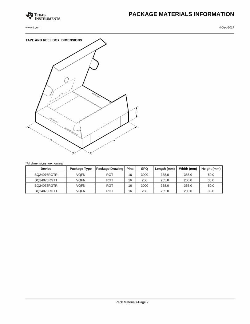
*All dimensions are nominal
Device Package Type Package Drawing Pins SPQ Length (mm) Width (mm) Height (mm)
BQ24076RGTR VQFN RGT 16 3000 338.0 355.0 50.0
BQ24076RGTT VQFN RGT 16 250 205.0 200.0 33.0
BQ24078RGTR VQFN RGT 16 3000 338.0 355.0 50.0
BQ24078RGTT VQFN RGT 16 250 205.0 200.0 33.0
PACKAGE MATERIALS INFORMATION
www.ti.com 4-Dec-2017
Pack Materials-Page 2
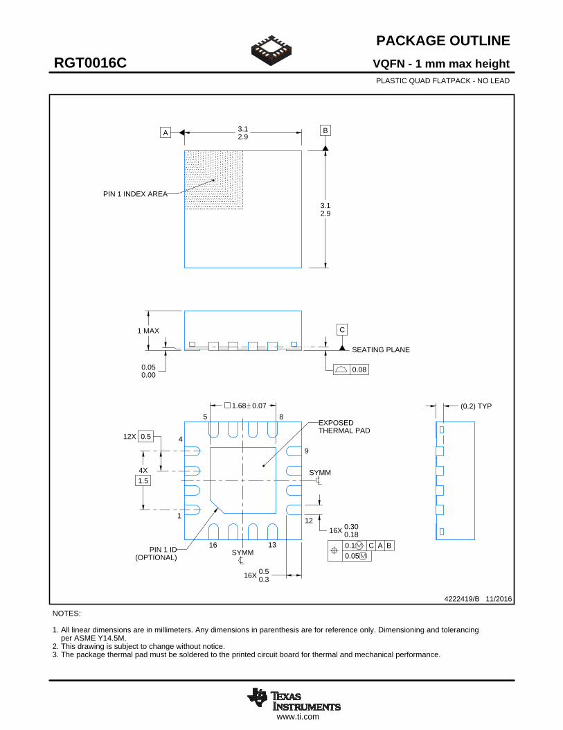
www.ti.com
PACKAGE OUTLINE
C
16X 0.300.18
1.68 0.07
16X 0.50.3
1 MAX
(0.2) TYP
0.050.00
12X 0.5
4X1.5
A 3.12.9
B
3.12.9
VQFN - 1 mm max heightRGT0016CPLASTIC QUAD FLATPACK - NO LEAD
4222419/B 11/2016
PIN 1 INDEX AREA
0.08
SEATING PLANE
1
49
12
5 8
16 13
(OPTIONAL)PIN 1 ID 0.1 C A B
0.05
EXPOSEDTHERMAL PAD
SYMM
SYMM
NOTES: 1. All linear dimensions are in millimeters. Any dimensions in parenthesis are for reference only. Dimensioning and tolerancing per ASME Y14.5M. 2. This drawing is subject to change without notice. 3. The package thermal pad must be soldered to the printed circuit board for thermal and mechanical performance.
SCALE 3.600
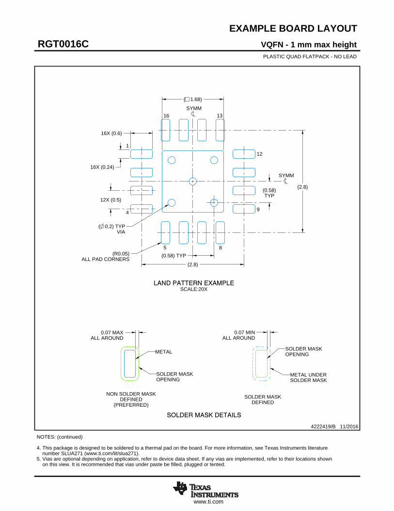
www.ti.com
EXAMPLE BOARD LAYOUT
0.07 MINALL AROUND
0.07 MAXALL AROUND
16X (0.24)
16X (0.6)
( 0.2) TYPVIA
12X (0.5)
(2.8)
(2.8)
(0.58)TYP
( 1.68)
(R0.05)ALL PAD CORNERS
(0.58) TYP
VQFN - 1 mm max heightRGT0016CPLASTIC QUAD FLATPACK - NO LEAD
4222419/B 11/2016
SYMM
1
4
5 8
9
12
1316
SYMM
LAND PATTERN EXAMPLESCALE:20X
NOTES: (continued) 4. This package is designed to be soldered to a thermal pad on the board. For more information, see Texas Instruments literature number SLUA271 (www.ti.com/lit/slua271).5. Vias are optional depending on application, refer to device data sheet. If any vias are implemented, refer to their locations shown on this view. It is recommended that vias under paste be filled, plugged or tented.
SOLDER MASKOPENING
METAL UNDERSOLDER MASK
SOLDER MASKDEFINED
METAL
SOLDER MASKOPENING
SOLDER MASK DETAILS
NON SOLDER MASKDEFINED
(PREFERRED)
www.ti.com
EXAMPLE STENCIL DESIGN
16X (0.6)
16X (0.24)
12X (0.5)
(2.8)
(2.8)
( 1.55)
(R0.05) TYP
VQFN - 1 mm max heightRGT0016CPLASTIC QUAD FLATPACK - NO LEAD
4222419/B 11/2016
NOTES: (continued) 6. Laser cutting apertures with trapezoidal walls and rounded corners may offer better paste release. IPC-7525 may have alternate design recommendations.
SYMM
ALL AROUNDMETAL
SOLDER PASTE EXAMPLEBASED ON 0.125 mm THICK STENCIL
EXPOSED PAD 17:
85% PRINTED SOLDER COVERAGE BY AREA UNDER PACKAGESCALE:25X
SYMM
1
4
5 8
9
12
1316
17

IMPORTANT NOTICE
Texas Instruments Incorporated (TI) reserves the right to make corrections, enhancements, improvements and other changes to itssemiconductor products and services per JESD46, latest issue, and to discontinue any product or service per JESD48, latest issue. Buyersshould obtain the latest relevant information before placing orders and should verify that such information is current and complete.TI’s published terms of sale for semiconductor products (http://www.ti.com/sc/docs/stdterms.htm) apply to the sale of packaged integratedcircuit products that TI has qualified and released to market. Additional terms may apply to the use or sale of other types of TI products andservices.Reproduction of significant portions of TI information in TI data sheets is permissible only if reproduction is without alteration and isaccompanied by all associated warranties, conditions, limitations, and notices. TI is not responsible or liable for such reproduceddocumentation. Information of third parties may be subject to additional restrictions. Resale of TI products or services with statementsdifferent from or beyond the parameters stated by TI for that product or service voids all express and any implied warranties for theassociated TI product or service and is an unfair and deceptive business practice. TI is not responsible or liable for any such statements.Buyers and others who are developing systems that incorporate TI products (collectively, “Designers”) understand and agree that Designersremain responsible for using their independent analysis, evaluation and judgment in designing their applications and that Designers havefull and exclusive responsibility to assure the safety of Designers' applications and compliance of their applications (and of all TI productsused in or for Designers’ applications) with all applicable regulations, laws and other applicable requirements. Designer represents that, withrespect to their applications, Designer has all the necessary expertise to create and implement safeguards that (1) anticipate dangerousconsequences of failures, (2) monitor failures and their consequences, and (3) lessen the likelihood of failures that might cause harm andtake appropriate actions. Designer agrees that prior to using or distributing any applications that include TI products, Designer willthoroughly test such applications and the functionality of such TI products as used in such applications.TI’s provision of technical, application or other design advice, quality characterization, reliability data or other services or information,including, but not limited to, reference designs and materials relating to evaluation modules, (collectively, “TI Resources”) are intended toassist designers who are developing applications that incorporate TI products; by downloading, accessing or using TI Resources in anyway, Designer (individually or, if Designer is acting on behalf of a company, Designer’s company) agrees to use any particular TI Resourcesolely for this purpose and subject to the terms of this Notice.TI’s provision of TI Resources does not expand or otherwise alter TI’s applicable published warranties or warranty disclaimers for TIproducts, and no additional obligations or liabilities arise from TI providing such TI Resources. TI reserves the right to make corrections,enhancements, improvements and other changes to its TI Resources. TI has not conducted any testing other than that specificallydescribed in the published documentation for a particular TI Resource.Designer is authorized to use, copy and modify any individual TI Resource only in connection with the development of applications thatinclude the TI product(s) identified in such TI Resource. NO OTHER LICENSE, EXPRESS OR IMPLIED, BY ESTOPPEL OR OTHERWISETO ANY OTHER TI INTELLECTUAL PROPERTY RIGHT, AND NO LICENSE TO ANY TECHNOLOGY OR INTELLECTUAL PROPERTYRIGHT OF TI OR ANY THIRD PARTY IS GRANTED HEREIN, including but not limited to any patent right, copyright, mask work right, orother intellectual property right relating to any combination, machine, or process in which TI products or services are used. Informationregarding or referencing third-party products or services does not constitute a license to use such products or services, or a warranty orendorsement thereof. Use of TI Resources may require a license from a third party under the patents or other intellectual property of thethird party, or a license from TI under the patents or other intellectual property of TI.TI RESOURCES ARE PROVIDED “AS IS” AND WITH ALL FAULTS. TI DISCLAIMS ALL OTHER WARRANTIES ORREPRESENTATIONS, EXPRESS OR IMPLIED, REGARDING RESOURCES OR USE THEREOF, INCLUDING BUT NOT LIMITED TOACCURACY OR COMPLETENESS, TITLE, ANY EPIDEMIC FAILURE WARRANTY AND ANY IMPLIED WARRANTIES OFMERCHANTABILITY, FITNESS FOR A PARTICULAR PURPOSE, AND NON-INFRINGEMENT OF ANY THIRD PARTY INTELLECTUALPROPERTY RIGHTS. TI SHALL NOT BE LIABLE FOR AND SHALL NOT DEFEND OR INDEMNIFY DESIGNER AGAINST ANY CLAIM,INCLUDING BUT NOT LIMITED TO ANY INFRINGEMENT CLAIM THAT RELATES TO OR IS BASED ON ANY COMBINATION OFPRODUCTS EVEN IF DESCRIBED IN TI RESOURCES OR OTHERWISE. IN NO EVENT SHALL TI BE LIABLE FOR ANY ACTUAL,DIRECT, SPECIAL, COLLATERAL, INDIRECT, PUNITIVE, INCIDENTAL, CONSEQUENTIAL OR EXEMPLARY DAMAGES INCONNECTION WITH OR ARISING OUT OF TI RESOURCES OR USE THEREOF, AND REGARDLESS OF WHETHER TI HAS BEENADVISED OF THE POSSIBILITY OF SUCH DAMAGES.Unless TI has explicitly designated an individual product as meeting the requirements of a particular industry standard (e.g., ISO/TS 16949and ISO 26262), TI is not responsible for any failure to meet such industry standard requirements.Where TI specifically promotes products as facilitating functional safety or as compliant with industry functional safety standards, suchproducts are intended to help enable customers to design and create their own applications that meet applicable functional safety standardsand requirements. Using products in an application does not by itself establish any safety features in the application. Designers mustensure compliance with safety-related requirements and standards applicable to their applications. Designer may not use any TI products inlife-critical medical equipment unless authorized officers of the parties have executed a special contract specifically governing such use.Life-critical medical equipment is medical equipment where failure of such equipment would cause serious bodily injury or death (e.g., lifesupport, pacemakers, defibrillators, heart pumps, neurostimulators, and implantables). Such equipment includes, without limitation, allmedical devices identified by the U.S. Food and Drug Administration as Class III devices and equivalent classifications outside the U.S.TI may expressly designate certain products as completing a particular qualification (e.g., Q100, Military Grade, or Enhanced Product).Designers agree that it has the necessary expertise to select the product with the appropriate qualification designation for their applicationsand that proper product selection is at Designers’ own risk. Designers are solely responsible for compliance with all legal and regulatoryrequirements in connection with such selection.Designer will fully indemnify TI and its representatives against any damages, costs, losses, and/or liabilities arising out of Designer’s non-compliance with the terms and provisions of this Notice.
Mailing Address: Texas Instruments, Post Office Box 655303, Dallas, Texas 75265Copyright © 2017, Texas Instruments Incorporated